JP5728947B2 - Alignment mark forming method, nozzle substrate forming method, nozzle substrate and droplet discharge head - Google Patents
Alignment mark forming method, nozzle substrate forming method, nozzle substrate and droplet discharge head Download PDFInfo
- Publication number
- JP5728947B2 JP5728947B2 JP2011000987A JP2011000987A JP5728947B2 JP 5728947 B2 JP5728947 B2 JP 5728947B2 JP 2011000987 A JP2011000987 A JP 2011000987A JP 2011000987 A JP2011000987 A JP 2011000987A JP 5728947 B2 JP5728947 B2 JP 5728947B2
- Authority
- JP
- Japan
- Prior art keywords
- substrate surface
- groove
- substrate
- nozzle hole
- forming
- Prior art date
- Legal status (The legal status is an assumption and is not a legal conclusion. Google has not performed a legal analysis and makes no representation as to the accuracy of the status listed.)
- Active
Links
Images


Description
本発明は、基板の両面にアライメントマークを形成するアライメントマーク形成方法と、液滴を吐出するための複数のノズル孔を有するノズル基板の形成方法と、前記形成方法で形成されたノズル基板と、前記ノズル基板を搭載した液滴吐出ヘッドとに関する。 The present invention includes an alignment mark forming method for forming alignment marks on both sides of a substrate, a nozzle substrate forming method having a plurality of nozzle holes for discharging droplets, a nozzle substrate formed by the forming method, The present invention relates to a droplet discharge head on which the nozzle substrate is mounted.
従来、MEMS(Micro Electro Mechanical Systems)デバイス製造において、フォトリソグラフィー工程によって基板の両面にデバイス構造を加工する場合、基板の両面にデバイスの形状の露光を行なう両面露光装置が用いられている。両面露光装置を用いて、基板の両面にデバイスの形状の露光を行なう場合、マスクに描かれたデバイスの形状と、アライメントマークとを基板の表面(第1基板面)に露光し、転写を行なう。次に、基板を裏返して両面露光装置に載置し、基板の第1面に形成したアライメントマークもしくはデバイスの形状を基準に、基板の裏面(第2基板面)に形成するデバイスの形状のアライメントを行ない第2基板面に形成するデバイスの形状の露光と、転写とを行ない基板の両面にデバイスの形状を形成している。 2. Description of the Related Art Conventionally, in manufacturing a MEMS (Micro Electro Mechanical Systems) device, when a device structure is processed on both sides of a substrate by a photolithography process, a double-side exposure apparatus that exposes the shape of the device on both sides of the substrate is used. When exposing the shape of the device on both sides of the substrate using a double-sided exposure apparatus, the shape of the device drawn on the mask and the alignment mark are exposed on the surface of the substrate (first substrate surface) and transferred. . Next, the substrate is turned over and placed on a double-sided exposure apparatus, and the alignment of the shape of the device formed on the back surface (second substrate surface) of the substrate is based on the alignment mark formed on the first surface of the substrate or the shape of the device. The shape of the device is formed on both sides of the substrate by performing exposure and transfer of the shape of the device formed on the second substrate surface.
また、基板の裏面となる第2基板面のアライメントは、第2基板面に転写をおこなうデバイスの形状が描かれたマスク版のアライメントマークを、両面露光装置に付属のアライメント光学装置で撮像する。次に、裏面となっている第1基板面に形成した基準となるアライメントマークを裏面光学装置で撮像する。 The alignment of the second substrate surface, which is the back surface of the substrate, is performed by imaging an alignment mark on the mask plate on which the shape of a device that performs transfer on the second substrate surface is drawn with an alignment optical device attached to the double-side exposure apparatus. Next, the reference alignment mark formed on the first substrate surface which is the back surface is imaged by the back surface optical device.
さらに、アライメントモニター装置に裏面光学装置で撮像された第1基板面のアライメントマークと、アライメント光学装置で撮像された第2基板面に転写するデバイスの形状が描かれたマスク版のアライメントマーク像とを合成するし映し出す。そして、アライメントモニター装置に映し出されたアライメントマーク像を重ね合わせてアライメントをおこない基板にデバイスの形状を露光する方法が行なわれている。 Furthermore, the alignment mark image of the first substrate surface imaged by the back surface optical device on the alignment monitor device, and the alignment mark image of the mask plate on which the shape of the device to be transferred to the second substrate surface imaged by the alignment optical device is drawn Synthesize and project. A method of aligning the alignment mark images projected on the alignment monitor device to perform alignment and exposing the shape of the device to the substrate is performed.
このように基板の両面露光を行なう場合、第2基板面となる基板面の露光は、基準となる第1基板面に形成したアライメントマークなどを光学装置で撮像し、第2基板面に転写するデバイスの形状が描かれたマスク版のアライメントマークと、第1基板面に形成したアライメントマークとを用いてアライメントを行なうことによって、基板の両面にデバイスの形状の露光と、転写とを行なっていた。 When performing double-sided exposure of the substrate in this way, the exposure of the substrate surface serving as the second substrate surface is performed by imaging an alignment mark or the like formed on the reference first substrate surface with an optical device and transferring the image to the second substrate surface. By performing alignment using the alignment mark of the mask plate on which the device shape is drawn and the alignment mark formed on the first substrate surface, the device shape is exposed and transferred on both surfaces of the substrate. .
このため、基板の片面に露光を行なう場合に比べて基板の両面に露光を行なう場合は、裏面となる基板面に転写されているアライメントマークを撮像する光学装置と、マスク版に描かれたアライメントマークを撮像する光学装置との誤差によって、相対する基板の第1基板面と、第2基板面とにデバイスの形状を形成するアライメント精度が劣るという課題があった。 For this reason, in the case where exposure is performed on both sides of the substrate as compared with the case where exposure is performed on one side of the substrate, an optical device for imaging the alignment mark transferred to the substrate surface serving as the back surface and the alignment drawn on the mask plate There has been a problem that alignment accuracy for forming a device shape on the first substrate surface and the second substrate surface of the opposing substrate is inferior due to an error with the optical apparatus that images the mark.
特許文献1では、デバイスを形成する基板の第1基板面と、第2基板面とを貫通する貫通マーク(孔)を形成する貫通マーク形成工程を備え、貫通マークを基準に第1基板面および第2基板面と、マスクに描かれたアライメントマークとをアライメントするアライメントマーク形成方法と、そのアライメントマーク形成方法を用いる圧電振動(MEMS)デバイスの製造方法が開示されている。
しかしながら、基板に貫通マーク、換言すればアライメントマークを形成する場合、貫通孔を穿孔する工程と、その穿孔工程を実行する装置とが必要となり新たな工程と、装置とを要することになる。また、貫通孔を設けることでデバイスを形成できる領域が少なくなるという課題があった。従って、基板にアライメントマークを穿孔およびデバイスが形成できる領域が浸食されずに、基板の両面のアライメントが出来るアライメントマーク形成方法と、その方法を用いたノズル基板などのMEMSデバイスが要望されていた。 However, when a through mark, in other words, an alignment mark is formed on a substrate, a step of drilling a through hole and a device for performing the drilling step are required, and a new step and a device are required. Moreover, the subject that the area | region which can form a device decreases by providing a through-hole occurred. Therefore, there has been a demand for an alignment mark forming method that can align both surfaces of a substrate without eroding an area where an alignment mark can be drilled and a device can be formed on the substrate, and a MEMS device such as a nozzle substrate using the method.
また、相対する基板の両面にデバイスを形成する場合、両面露光装置のアライメント光学装置の誤差によって、デバイスを形成する位置ズレが生じ、MEMSデバイスの品質を低下させる課題があった。従って、アライメント光学装置等の誤差が生じやすい両面露光装置を用いることなく基板の両面にデバイスの形状の形成をすることができるアライメントマークの形成方法と、その方法を用いたノズル基板などのMEMSデバイスが要望されていた。 In addition, when devices are formed on both surfaces of opposing substrates, there is a problem in that the position of the device is shifted due to an error in the alignment optical apparatus of the double-side exposure apparatus, and the quality of the MEMS device is deteriorated. Therefore, a method for forming an alignment mark that can form a device shape on both sides of a substrate without using a double-sided exposure apparatus such as an alignment optical apparatus that is likely to cause an error, and a MEMS device such as a nozzle substrate using the method Was requested.
本発明は、上述した課題の少なくとも一部を解決するためになされたものであり、以下の形態または適用例として実現することが可能である。 SUMMARY An advantage of some aspects of the invention is to solve at least a part of the problems described above, and the invention can be implemented as the following forms or application examples.
(適用例1)本適用例に係るアライメントマーク形成方法は、第1基板面と当該第1基板面に相対する第2基板面とを有する基板に対し、第1基板面に所定の深さの溝を形成する溝形成工程と、溝に充填された状態で溝を保護する第1保護膜を形成する第1保護膜形成工程と、溝が第2基板面に露出するように第2基板面を研削する研削工程とを備え、第1基板面と、第2基板面とに形成された溝をアライメントマークとして用いることを特徴とする。 Application Example 1 An alignment mark forming method according to this application example has a predetermined depth on the first substrate surface with respect to a substrate having a first substrate surface and a second substrate surface opposite to the first substrate surface. A groove forming step for forming a groove, a first protective film forming step for forming a first protective film for protecting the groove in a state where the groove is filled, and a second substrate surface so that the groove is exposed on the second substrate surface. And a groove formed on the first substrate surface and the second substrate surface is used as an alignment mark.
このようなアライメントマーク形成方法によれば、第1基板面に溝を形成し、形成した溝に第1保護膜を充填し、さらに第2基板面を研削することで第2基板面に第1保護膜で充填された溝が露出する。このことによって、第1基板面と、第2基板面との相対する同じ位置に非貫通の溝が形成される。従って、第1基板面と、第2基板面との相対する同じ位置に形成された溝をアライメントマークとして用いることで、第1基板面と、第2基板面とにおこなうアライメントの位置ズレを抑制できるアライメントマークの形成ができる。 According to such an alignment mark formation method, a groove is formed on the first substrate surface, the formed groove is filled with the first protective film, and the second substrate surface is ground, whereby the first substrate surface is ground. The groove filled with the protective film is exposed. As a result, a non-penetrating groove is formed at the same opposing position on the first substrate surface and the second substrate surface. Therefore, by using a groove formed at the same position opposite to the first substrate surface and the second substrate surface as an alignment mark, it is possible to suppress misalignment of alignment between the first substrate surface and the second substrate surface. An alignment mark that can be formed can be formed.
(適用例2)上記適用例に係るアライメントマーク形成方法において、溝は、第1基板面または第2基板面に形成されるデバイスの輪郭形状を用いていることが好ましい。 Application Example 2 In the alignment mark forming method according to the application example, it is preferable that the groove uses a contour shape of a device formed on the first substrate surface or the second substrate surface.
このようなアライメントマーク形成方法によれば、アライメントマークとなる溝として第1基板面または第2基板面に形成されるデバイスの輪郭形状を用いることで、輪郭形状となるデバイスのアライメントは輪郭形状に沿ってアライメントをおこなうことができる。従って、形成されるデバイスの形状と、アライメントマークとなる輪郭形状とを重ねることでアライメントを容易におこなうことができる。 According to such an alignment mark formation method, by using the contour shape of the device formed on the first substrate surface or the second substrate surface as the groove to be the alignment mark, the alignment of the device to be the contour shape is changed to the contour shape. Alignment can be performed. Therefore, alignment can be easily performed by overlapping the shape of the device to be formed and the contour shape to be the alignment mark.
(適用例3)上記適用例に係るアライメントマーク形成方法において、アライメントマークとなる溝の深さは、基板の厚さ未満の深さであることが好ましい。 Application Example 3 In the alignment mark forming method according to the application example described above, the depth of the groove to be the alignment mark is preferably less than the thickness of the substrate.
このようなアライメントマーク形成方法によれば、アライメントマークとなる溝の深さを、基板の厚さ未満とすることで、溝を保護する第1保護膜を溝に充填し、形成することができる。 According to such an alignment mark forming method, the groove can be formed by filling the groove with the first protective film for protecting the groove by setting the depth of the groove serving as the alignment mark to be less than the thickness of the substrate. .
(適用例4)上記適用例に係るアライメントマーク形成方法において、第1基板面には第1デバイスが形成され、第2基板面には第2デバイスが形成される場合、溝が形成される所定の深さは、第1デバイスの深さと第2デバイスの深さとを加えた深さ以上で、基板の厚さ未満であることが好ましい。 Application Example 4 In the alignment mark forming method according to the application example, when the first device is formed on the first substrate surface and the second device is formed on the second substrate surface, a groove is formed. The depth of is preferably equal to or greater than the sum of the depth of the first device and the depth of the second device, and less than the thickness of the substrate.
このようなアライメントマーク形成方法によれば、アライメントマークとなる溝の深さを、第1デバイスの深さと、第2デバイスの深さとを加えた深さ以上で、基板の厚さ未満とすることで、アライメントマークとなる溝の形状に内接する基板を貫通することなく溝を形成することができる。 According to such an alignment mark forming method, the depth of the groove serving as the alignment mark is equal to or greater than the depth of the first device and the second device, and less than the thickness of the substrate. Thus, the groove can be formed without penetrating the substrate inscribed in the shape of the groove serving as the alignment mark.
(適用例5)本適用例に係るノズル基板形成方法は、第2基板面に形成され、液滴を吐出する液状体を貯留する第2ノズル孔の輪郭形状を、第1基板面の相対する位置に所定の深さで溝状に輪郭溝を形成する溝形成工程としての輪郭溝形成工程と、輪郭溝に充填された状態で輪郭溝を保護する第1保護膜を形成する第1保護膜形成工程と、第1基板面に形成された輪郭溝による輪郭形状を基準として、第1基板面に液滴を吐出する第1ノズル孔を形成する第1ノズル孔形成工程と、第1ノズル孔を保護する第2保護膜形成工程と、輪郭溝が第2基板面に露出するように第2基板面を研削する研削工程と、第2基板面に露出した輪郭溝による輪郭形状を基準として、第2保護膜が露出するように第2ノズル孔を形成する第2ノズル孔形成工程と、第1ノズル孔と第2ノズル孔を液状体から保護する第3保護膜を形成する第3保護膜形成工程とを備えることを特徴とする。 (Application Example 5) In the nozzle substrate forming method according to this application example, the contour shape of the second nozzle hole formed on the second substrate surface for storing the liquid material for discharging the droplets is opposed to the first substrate surface. A contour groove forming step as a groove forming step for forming a contour groove in a groove shape at a predetermined depth at a position, and a first protective film for forming a first protective film for protecting the contour groove in a state of being filled in the contour groove A forming step, a first nozzle hole forming step for forming a first nozzle hole for discharging droplets on the first substrate surface with reference to a contour shape formed by a contour groove formed on the first substrate surface, and a first nozzle hole The second protective film forming step for protecting the substrate, the grinding step for grinding the second substrate surface so that the contour groove is exposed on the second substrate surface, and the contour shape by the contour groove exposed on the second substrate surface, A second nozzle hole forming step of forming the second nozzle hole so that the second protective film is exposed; A first nozzle hole and second nozzle hole, characterized in that it comprises a third protective film forming step of forming a third protective film for protecting from the liquid material.
このようなノズル基板形成方法によれば、第2基板面に形成される第2ノズル孔の輪郭形状を、第1基板面の相対する位置に溝状の輪郭溝を形成し、形成した輪郭溝に第1保護膜を充填された状態に形成し、さらに第2基板面を研削することで、第1基板面と、第2基板面との相対する同じ位置にアライメントマークとなる輪郭溝を形成することができる。 According to such a nozzle substrate forming method, the contour shape of the second nozzle hole formed on the second substrate surface is formed as a groove-shaped contour groove at a position opposite to the first substrate surface, and the contour groove thus formed is formed. Is formed in a state filled with the first protective film, and further, the second substrate surface is ground to form a contour groove serving as an alignment mark at the same position facing the first substrate surface and the second substrate surface. can do.
また、第2基板面に形成する第2ノズル孔は、第2ノズル孔の輪郭形状である輪郭溝に沿って内側に形成することから、第2基板面に形成する第2ノズル孔のアライメントは、輪郭溝の幅の精度誤差が許容されアライメント精度を緩和することができる。 Moreover, since the 2nd nozzle hole formed in the 2nd substrate surface is formed inside along the outline groove | channel which is the outline shape of the 2nd nozzle hole, the alignment of the 2nd nozzle hole formed in the 2nd substrate surface is An accuracy error in the width of the contour groove is allowed and the alignment accuracy can be relaxed.
また、第2ノズル孔形成工程によって、第2保護膜が露出するように第2ノズル孔を形成することで、第1ノズル孔を損傷することなく第1ノズル孔と連通する第2ノズル孔を形成することができる。 Further, by forming the second nozzle hole so that the second protective film is exposed by the second nozzle hole forming step, the second nozzle hole communicating with the first nozzle hole without damaging the first nozzle hole is formed. Can be formed.
また、第3保護膜を第1基板面および第2基板面と、第1ノズル孔および第2ノズル孔とに形成することで、吐出する液滴の浸食から保護することができる。 Further, by forming the third protective film on the first substrate surface and the second substrate surface, and the first nozzle hole and the second nozzle hole, it is possible to protect against the erosion of the discharged droplets.
従って、片面アライメント装置を用いて、第1基板面と、第2基板面とに形成する第1ノズル孔と、第2ノズル孔とのアライメントができ、同心円の精度が高い第1ノズル孔と、第2ノズル孔を形成できるノズル基板の形成方法を実現できる。 Therefore, using the single-sided alignment device, the first nozzle hole formed on the first substrate surface and the second substrate surface can be aligned with the second nozzle hole, and the first nozzle hole having high concentric accuracy, A nozzle substrate forming method capable of forming the second nozzle holes can be realized.
(適用例6)本適用例に係るノズル基板は、上述のノズル基板の製造方法を用いて製造されたこと、を特徴とする。 Application Example 6 A nozzle substrate according to this application example is manufactured using the nozzle substrate manufacturing method described above.
このようなノズル基板によれば、第1ノズル孔と、第2ノズル孔とを同じアライメントマークとなる輪郭溝を基準にアライメントをおこない形成することから、同心円精度の高い第1ノズル孔と、第2ノズル孔とを有するノズル基板ができる。従って、第1ノズル孔から吐出される液滴の飛翔方向と、液滴量とを一定に保つことができるノズル基板を実現できる。 According to such a nozzle substrate, the first nozzle hole and the second nozzle hole are aligned and formed with reference to the contour groove serving as the same alignment mark, so the first nozzle hole with high concentric accuracy, A nozzle substrate having two nozzle holes is obtained. Therefore, it is possible to realize a nozzle substrate that can keep the flying direction of the droplets discharged from the first nozzle holes and the amount of the droplets constant.
(適用例7)本適用例に係る液滴吐出ヘッドは、上述したノズル基板を用いて製造されたことを特徴とする。 Application Example 7 A droplet discharge head according to this application example is manufactured using the nozzle substrate described above.
このような液滴吐出ヘッドによれば、上述したノズル基板を液滴吐出ヘッドに用いることで、複数のノズル孔から吐出される液滴の飛翔方向と、液滴の量とを一定に保つことができ、液滴吐出精度が高い液滴吐出ヘッドが実現できる。 According to such a droplet discharge head, by using the above-described nozzle substrate for the droplet discharge head, the flying direction of the droplets discharged from the plurality of nozzle holes and the amount of the droplets can be kept constant. And a droplet discharge head with high droplet discharge accuracy can be realized.
以下、実施形態を図面に基づいて、基板の両面にアライメントマークを形成する形成方法と、液滴を吐出するためのノズル孔を有するノズル基板の形成方法と、その形成方法を用いて形成されたノズル基板と、そのノズル基板を用いた液滴吐出ヘッドとについて説明する。なお、以下に示す各図においては、各構成要素を図面上で認識され得る程度の大きさとするため、各構成要素の寸法や比率を実際の構成要素とは適宜に異ならせて記載をしている。 Hereinafter, embodiments are formed using a forming method for forming alignment marks on both sides of a substrate, a forming method for a nozzle substrate having nozzle holes for discharging droplets, and the forming method based on the drawings. A nozzle substrate and a droplet discharge head using the nozzle substrate will be described. In the drawings shown below, the dimensions and ratios of the respective constituent elements are described differently from the actual constituent elements in order to make each constituent element large enough to be recognized on the drawings. Yes.
(第1実施形態)
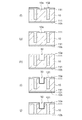
以下、本実施形態を図面に沿って説明する。図1は、第1実施形態に係る第1基板面1aと、当該第1基板面1aに相対する第2基板面1bとを有する基板1の両面にアライメントマークを形成するアライメントマーク形成方法を工程順に示す模式図である。図1を参照して、アライメントマーク形成方法を工程順に説明する。
(First embodiment)
Hereinafter, the present embodiment will be described with reference to the drawings. FIG. 1 shows an alignment mark forming method for forming alignment marks on both surfaces of a
本実施形態のアライメントマーク形成方法は、第1基板面1aと、当該第1基板面1aに相対する第2基板面1bとを有する基板1の第1基板面1aにアライメントマークとなる溝2を形成する。次に、第1基板面1aに形成された溝2に第1保護膜111を充填された状態で形成し、さらに第2基板面1bを研削し、第1基板面1aから形成された溝2を露出させることで、第1基板面1aと、第2基板面1bとの相対する同じ位置にアライメントマークとなる溝2を形成する。なお、本実施形態のアライメントマークを形成する基板1はシリコン基板を用いている。
In the alignment mark forming method of the present embodiment, a
次に本実施形態のアライメントマーク形成工程は、アライメントマークとなる溝2の形状を第1基板面1aに転写をする第1フォト工程を備える。また、転写された溝2の形状をエッチングによって、溝2を形成する溝形成工程と、第1フォト工程で溝2の転写に用いた第1レジスト膜101を剥離する第1剥離工程とを備える。また、溝2に充填された状態で、溝2を保護する第1保護膜111を形成する第1保護膜形成工程と、第1基板面1aに形成した溝2を、第2基板面1bを研削することによって第2基板面1bに露出させる研削工程とを備えている。
Next, the alignment mark forming step of the present embodiment includes a first photo step of transferring the shape of the
図1(a)は、溝2の形状を第1基板面1aに転写する第1フォト工程を示す模式図である。図1(a)に示すように第1フォト工程は、第1基板面1aに感光材料(以下、「レジスト」と称する。)を塗付し、第1レジスト膜101の形成をおこなう。次に、溝2の形状が描かれたマスク版(不図示)と、第1レジスト膜101が形成された第1基板面1aとを対向させて配置する。次に、マスク版に描かれた溝2の形状を第1基板面1aに形成された第1レジスト膜101へ露光によって転写し、第1基板面1a上にアライメントマークとなる溝2の形状を転写する。次に、露光によって溝2の形状が転写された第1レジスト膜101の現像をおこない、溝2の形状の第1レジスト膜101が剥離され第1基板面1aを露出させる。
FIG. 1A is a schematic diagram showing a first photo process for transferring the shape of the
次に図1(b)は、前述の第1フォト工程で第1基板面1aに転写された溝2の形状をエッチングによって溝2を形成する溝形成工程を示す模式図である。図1(b)に示すように溝形成工程は、前述の第1フォト工程で転写された溝2の形状をエッチングによって溝2を形成する。溝形成工程によって形成する溝2は、溝2が形成される当該基板1の厚さ未満の深さの溝2を形成する。
Next, FIG. 1B is a schematic view showing a groove forming step for forming the
次に図1(c)は、前述の第1フォト工程で溝2の形状を転写するために用いた第1レジスト膜101を剥離する第1剥離工程を模式的に示す図である。図1(c)に示すように第1剥離工程は、前述の第1フォト工程で溝2の形状を転写するために用いた第1レジスト膜101の剥離を行なう。第1レジスト膜101の剥離は、硫酸などを含んだ水溶液に基板1を浸漬し、水溶液が付着した基板1の水洗をおこなうことで、第1基板面1aから第1レジスト膜101の剥離をおこなう。
Next, FIG. 1C is a diagram schematically showing a first peeling process for peeling the first resist
次に図1(d)は、前述の溝形成工程で形成した溝2を保護する第1保護膜111を形成する第1保護膜形成工程を模式的に示す図である。図1(d)に示すように第1保護膜形成工程は、溝形成工程で形成された溝2に充填された状態で溝2を保護する第1保護膜111を形成する。なお、本実施形態の第1保護膜111は酸化膜で溝2を充填し、酸化膜の形成は熱酸化法によって形成をおこなう。
Next, FIG. 1D schematically shows a first protective film forming step for forming a first
次に図(e)は、前述の溝形成工程で形成された溝2を第2基板面1bに露出させる研削工程を示す模式図である。図1(e)に示すように研削工程は、第1基板面1aから溝形成工程によって形成された溝2が第2基板面1bに露出するまで第2基板面1bの研削をおこなう。第2基板面1bの研削は、ダイヤモンド粒などを含む研削ホイールを備えた研削装置(不図示)で研削をおこなう。研削が完了すると、第2基板面1bに第1保護膜111が充填されたアライメント孔となる溝2が露出し、一連のアライメントマーク形成工程が完了する。
Next, FIG. (E) is a schematic diagram showing a grinding process for exposing the
上述した第1実施形態によれば、以下の効果が得られる。
本実施形態のアライメントマーク形成方法は、第1基板面1aにアライメントマークとなる溝2を形成し、形成した溝2に第1保護膜111を充填し、さらに第2基板面1bを研削することで、第2基板面1bに第1保護膜111で充填された溝2が露出する。このことによって、第1基板面1aと、第2基板面1bとの相対する同じ位置に非貫通の溝2が形成される。従って、第1基板面1aと、第2基板面1bとの相対する同じ位置に形成された溝2をアライメントマークとして用いることで、第1基板面1aと、第2基板面1bとにおこなうアライメントの位置ズレを抑制できるアライメントマークの形成ができる。
According to the first embodiment described above, the following effects can be obtained.
In the alignment mark forming method of the present embodiment, a
また、溝2を保護する第1保護膜111として酸化膜を熱酸化法で形成し、溝2に充填することで、第1保護膜111と、溝2の壁である基板1とが分子結合し、溝2に充填された第1保護膜111は基板1と同等の強度を得ることができる。このことにより、アライメントマークとなる溝2が研削工程によって第2基板面1bに露出しても溝2と、溝2に内接する基板1とを貫通することなくアライメントマークを形成できる。従って、基板1の片面にアライメントを行なう片面露光装置を用いて基板1の両面のアライメントを精度高く行うことができる。
Further, an oxide film is formed as a first
(第2実施形態)
本実施形態は、アライメントマークとして第1基板面1aまたは第2基板面1bに形成するデバイスの輪郭形状を用いる点で、前述の第1実施形態で説明をしたアライメントマーク形成方法と異なっている。その他のアライメントマーク形成方法および形成工程は前述の第1実施形態と同様のため、同様の部分は構成および工程には同様の符号を付して説明は省略または簡略とする。
(Second Embodiment)
The present embodiment is different from the alignment mark forming method described in the first embodiment in that the contour shape of the device formed on the
以下、第1実施形態と相違する工程について図1を参照して説明する。
本実施形態のアライメントマーク形成工程は、第1基板面1aまたは第2基板面1bに形成するデバイスの輪郭形状を第1基板面1aに転写をする第1フォト工程をおこなう。
Hereinafter, steps different from those of the first embodiment will be described with reference to FIG.
In the alignment mark forming process of the present embodiment, a first photo process is performed in which the contour shape of the device formed on the
本実施形態のアライメントマーク形成方法は、第1基板面1aと、当該第1基板面1aに相対する第2基板面1bとを有する基板1の第1基板面1aに、アライメントマークとなる第1基板面1aまたは第2基板面1bに形成されるデバイスの輪郭形状の輪郭溝20を形成する。次に第1実施形態と同様に、第1基板面1aに形成された輪郭溝20に充填された状態で第1保護膜111を形成し、さらに第2基板面1bを研削し、第1基板面1aから形成された輪郭溝20を露出させることで、第1基板面1aと、第2基板面1bとの相対する同じ位置にアライメントマークとなる輪郭溝20を形成する。なお、本実施形態のアライメントマークを形成する基板1はシリコン基板を用いている。
In the alignment mark forming method of the present embodiment, the
次に本実施形態のアライメントマーク形成工程は、第1実施形態と同様にアライメントマークとなるデバイスの輪郭形状を第1基板面1aに転写をする第1フォト工程を備える。また、転写されたデバイスの輪郭形状をエッチングによって輪郭溝20に形成する輪郭溝形成工程と、第1フォト工程でデバイスの輪郭形状の転写に用いた第1レジスト膜101を剥離する第1剥離工程とを備える。また、輪郭溝20に充填された状態で輪郭溝20を保護する第1保護膜111を形成する第1保護膜形成工程と、第1基板面1aに形成した輪郭溝20を、第2基板面1bを研削することによって、第2基板面1bに露出させる研削工程とを備えている。
Next, the alignment mark forming process of the present embodiment includes a first photo process for transferring the contour shape of the device to be the alignment mark to the
次に、図1(b)を参照して前述の第1フォト工程で第1基板面1aに転写されたデバイスの輪郭形状をエッチングによって輪郭溝20を形成する輪郭溝形成工程について説明する。輪郭溝形成工程は、前述の第1フォト工程で転写されたデバイスの輪郭形状をエッチングによって輪郭溝20を形成する。輪郭溝形成工程によって形成する輪郭溝20は、第1基板面1aに形成される第1デバイスの深さと、第2基板面1bに形成される第2デバイスの深さとを加えた深さ以上で、当該基板1の厚み未満の深さの輪郭溝20を形成する。なお、本実施形態の輪郭溝形成工程はドライエッチングによって輪郭溝20の形成をおこなう。
Next, the contour groove forming step for forming the
次に、前述のフォト工程で形成した第1レジスト膜101を剥離する第1剥離工程と、前述の輪郭溝形成工程で形成した輪郭溝20に保護膜を形成する第1保護膜形成工程と、第1基板面1aに形成された輪郭溝20を研削工程によって第2基板面1bに露出させる研削工程とは第1実施形態と同様のため説明を省略する。
Next, a first peeling process for peeling the first resist
上述した第2実施形態によれば、以下の効果が得られる。
本実施形態のアライメントマーク形成方法は、アライメントマークとして第1基板面1aまたは第2基板面1bに形成するデバイスの輪郭形状を転写し、第1基板面1aにエッチングによって溝状に輪郭溝20を形成する。さらに、形成した輪郭溝20に第1保護膜111を充填し、第2基板面1bを研削し、輪郭溝20を露出する。このことによって、第1基板面1aと、第2基板面1bとの相対する位置に非貫通のアライメントマークを形成できる。
According to the second embodiment described above, the following effects can be obtained.
In the alignment mark forming method of the present embodiment, the contour shape of a device formed on the
このようなアライメントマーク形成方法によれば、アライメントマークとなる溝を第1基板面または第2基板面に形成されるデバイスの輪郭形状を用いることで、輪郭形状となるデバイスのアライメントは輪郭形状に沿ってアライメントをおこなうことができる。従って、形成されるデバイスの形状と、アライメントマークとなる輪郭形状とを重ねることでアライメントを容易におこなうことができる。また、形成されるデバイスの輪郭形状をアライメントマークとして用いることで、アライメントマークを形成する領域にもデバイスを形成することができる。 According to such an alignment mark forming method, by using the contour shape of the device formed on the first substrate surface or the second substrate surface as the groove to be the alignment mark, the alignment of the device that becomes the contour shape is changed to the contour shape. Alignment can be performed. Therefore, alignment can be easily performed by overlapping the shape of the device to be formed and the contour shape to be the alignment mark. Moreover, a device can be formed also in the area | region which forms an alignment mark by using the outline shape of the device formed as an alignment mark.
本実施形態のアライメントマーク形成方法は、輪郭溝形成工程で形成する輪郭溝20の深さを第1基板面1aに形成する第1デバイスの深さと、第2基板面に形成する第2デバイスの深さとを加えた深さ以上で、基板1の厚さ未満とすることで、輪郭溝20に内接する基板1が貫通されることなく輪郭溝20を形成することができる。
In the alignment mark forming method of the present embodiment, the depth of the
(第3実施形態)
図2から図4は、第3実施形態に係る第2実施形態で説明したアライメントマーク形成方法を用いたノズル基板10の形成方法を工程順に示す模式図である。図2から図4を参照して、ノズル基板10の形成方法を工程順に説明する。なお、第1実施形態と同様の工程は説明を簡略して説明をする。
(Third embodiment)
2 to 4 are schematic views showing a method of forming the
本実施形態のノズル基板10の形成方法は、第2実施形態で示したアライメントマーク形成方法を用いて、第1基板面10aと、相対する第2基板面10bとを有する基板1に複数のノズル孔50を形成する。第1基板面10aに液滴を吐出する孔となる複数の第1ノズル孔30と、第1ノズル孔30が形成された第1基板面10aに相対する第2基板面10bに、液滴を吐出する液状体を貯留し、第1ノズル孔30と同心円となる第2ノズル孔40とを有するノズル基板10を形成する。
The method for forming the
本実施形態のノズル基板10の形成工程は、第2基板面10bに形成する第2ノズル孔40の輪郭形状を第1基板面10aに転写する第1フォト工程と、第1基板面10aに転写された第2ノズル孔40の輪郭形状をエッチングによって溝状に形成する輪郭溝形成工程とを備える。
The formation process of the
また、輪郭溝20を保護する第1保護膜111を形成する第1保護膜形成工程と、第1ノズル孔30の形状を第1基板面10aに転写する第2フォト工程と、第1基板面10aに転写された第1ノズル孔30の形状をエッチングによって第1ノズル孔30を形成する第1ノズル孔形成工程とを備えている。また第2基板面10bを研削し、輪郭溝20を露出させる研削工程と、第2ノズル孔40の形状を第2基板面10bに転写する第3フォト工程と、第2基板面10bに転写された第2ノズル孔40の形状をエッチングによって第2ノズル孔40を形成する第2ノズル形成工程とを備える。
In addition, a first protective film forming step for forming the first
また、第2ノズル孔形成工程のエッチング反応によって、第1ノズル孔30が損傷することを保護する第2保護膜121を形成する第2保護膜形成工程と、第1ノズル孔30および第2ノズル孔40と、第1基板面1aおよび第2基板面1bとを液滴から保護する第3保護膜131を形成する第3保護膜形成工程とを備える。さらに、第1フォト工程から第3フォト工程で輪郭溝20または第1ノズル孔30または第2ノズル孔40の転写に用いた第1レジスト膜101から第3レジスト膜103を剥離する第1剥離工程から第3剥離工程を備えている。
The second protective film forming step for forming the second
図2(a)は、アライメントマークとなる第2ノズル孔40の輪郭形状を第1基板面10aに転写する第1フォト工程を示す模式図である。図2(a)に示すように本実施形態の第1フォト工程は、第1基板面10aにレジストを塗布し、第1レジスト膜101を形成する。次に、第2基板面10bに形成する第2ノズル孔40の輪郭形状が描かれたマスク版(不図示)と、第1レジスト膜101が形成された第1基板面10aとを対向させて配置する。次に、マスクに版に描かれた第2ノズル孔40の輪郭形状を第1基板面10aに形成された第1レジスト膜101へ露光によって転写し、第1基板面10a上に第2ノズル孔40の輪郭形状を転写する。次に、露光によって第2ノズル孔40の輪郭形状が転写された第1レジスト膜101の現像をおこなうことで、輪郭形状の第1レジスト膜101が剥離され、第1基板面1aを露出させる。
FIG. 2A is a schematic diagram showing a first photo process of transferring the contour shape of the
次に図2(b)は、前述の第1フォト工程で第1基板面10aに転写された第2ノズル孔40の輪郭形状をエッチングによって、溝状に輪郭溝20を形成する輪郭溝形成工程を示す模式図である。図2(b)に示すように本実施形態の輪郭溝形成工程は、前述の第1フォト工程で転写された輪郭形状をエッチングによって輪郭溝20を形成する。輪郭溝形成工程によって形成する輪郭溝20は、第1ノズル孔30の深さと、第2ノズル孔40の深さとを加えた深さ以上で、当該基板1の厚み未満の深さの輪郭溝20を形成する。なお、本実施形態の輪郭溝形成工程はドライエッチングによって輪郭溝20の形成をおこなう。
Next, FIG. 2B shows a contour groove forming step in which the
次に図2(c)は、前述の第1フォト工程で第2ノズル孔40の輪郭形状を転写するために用いた第1レジスト膜101を剥離する第1剥離工程を模式的に示す図である。図2(c)に示すように第1剥離工程は、第1実施形態と同様に前述の第1レジスト膜101の剥離をする。
Next, FIG. 2C schematically shows a first peeling process for peeling the first resist
次に図2(d)は、前述の輪郭溝形成工程で形成をした輪郭溝20を保護する第1保護膜111を形成する第1保護膜形成工程を模式的に示す図である。図2(d)に示すように第1保護膜形成工程は、第1実施形態と同様に輪郭溝形成工程で形成された輪郭溝20に充填された状態で輪郭溝20を保護する第1保護膜111を形成する。なお、第1保護膜111は第1実施形態と同様に酸化膜を熱酸化法によって形成する。
Next, FIG. 2D is a diagram schematically showing a first protective film forming step for forming the first
次に図2(e)は、第1ノズル孔30の形状を第1基板面10aに転写をする第2フォト工程を示す模式図である。図2(e)に示すように第2フォト工程は、第1フォト工程と同様に、第1保護膜111が形成された第1基板面10aに第2レジスト膜102を形成する。次に、マスク版(不図示)に描画された第1基板面10aに転写する第1ノズル孔30の形状を露光によって、第1基板面10aに形成した第2レジスト膜102に露光し、第1ノズル孔30の形状を転写する。次に、露光によって第1ノズル孔30の形状が転写された第2レジスト膜102の現像をおこなうことで、第1ノズル孔30の形状の第2レジスト膜102が剥離され、第1保護膜111を露出させる。
Next, FIG. 2E is a schematic diagram showing a second photo process for transferring the shape of the
第2フォト工程のアライメントは、第1基板面10aに形成された輪郭溝20をアライメントの基準として、マスク版に描かれた第1ノズル孔30の形状を第1基板面10aに露光し、転写をおこなう。
In the alignment of the second photo process, the shape of the
次に図3(f)は、後述の第1ノズル孔形成工程で第1ノズル孔30を形成する部分に形成されている第1保護膜111を除去する第1保護膜除去工程を模式的に示す図である。図3(f)に示すように第1保護膜除去工程は、前述の第2フォト工程で第1基板面10aに形成された第2レジスト膜102を露光し、転写された第1ノズル孔30の形状部分の第1保護膜111の除去をおこなう。第1保護膜111の除去は、エッチングによって第1保護膜111の除去をおこない第1ノズル孔30の形状部分の第1基板面10aを露出させる。
Next, FIG. 3F schematically shows a first protective film removing step for removing the first
次に図3(g)は、前述の第2フォト工程で第1ノズル孔30の形状を転写するために用いた第2レジスト膜102の剥離を行う第2剥離工程を模式的に示す図である。図3(g)に示すように第2剥離工程は、第1剥離工程と同様に前述の第2レジスト膜102の剥離を行なう。第2レジスト膜102の剥離後は、第1基板面10a上に 第1保護膜111が残存し、第1ノズル孔30を形成する形状の第1基板面10aが露出している状態となる。
Next, FIG. 3G schematically shows a second peeling step for peeling the second resist
次に図3(h)は、第1基板面10aに第1ノズル孔30を形成する第1ノズル孔形成工程を模式的に示す図である。図3(h)に示すように第1ノズル孔形成工程は、前述の第2フォト工程で転写された第1ノズル孔30の形状をエッチングによって、第1ノズル孔30を形成する。なお、本実施形態の第1ノズル孔形成工程は、ドライエッチングによって第1ノズル孔30を形成する。
Next, FIG. 3H is a diagram schematically showing a first nozzle hole forming step for forming the first nozzle holes 30 in the
次に図3(i)は、前述の第1ノズル形成工程で形成した第1ノズル孔30を、後述する第2ノズル孔形成工程のエッチング反応から保護をする第2保護膜121を形成する第2保護膜形成工程を模式的に示す図である。図3(i)に示すように第2保護膜形成工程は、前述の第1ノズル形成工程で形成した第1ノズル孔30を、後述する第2ノズル孔形成工程でおこなうエッチング反応から保護をする第2保護膜121を形成する。第2保護膜121は、前述の第1保護膜111と比べて薄膜の第2保護膜121を形成する。なお、本実施形態の第2保護膜121は、第1保護膜形成工程と同様に酸化膜を熱酸化法によって形成する。
Next, FIG. 3I shows a second
次に図3(j)は、前述の輪郭溝形成工程で形成した輪郭溝20を第2基板面10bに露出させるために第2基板面10bの研削を行なう研削工程を模式的に示す図である。図3(j)に示すように研削工程は、第1実施形態の研削工程と同様に第2基板面10bを研削し、輪郭溝形成工程によって第1基板面10aに形成された輪郭溝20が第2基板面10bに露出するまで第2基板面10bの研削をおこなう。
Next, FIG. 3J schematically shows a grinding process for grinding the
次に図4(k)は、第2ノズル孔40の形状を第2基板面10bに転写をする第3フォト工程を示す模式図である。図4(k)に示すように第3フォト工程は、第2フォト工程と同様に、第2基板面10bに第3レジスト膜103を形成し、マスク版(不図示)に描かれた第2基板面10bに形成する第2ノズル孔40の形状を露光によって、第2基板面10bに転写する。次に、露光によって第2ノズル孔40の形状が転写された第3レジスト膜103の現像をおこなうことで、第2ノズル孔40の形状の第3レジスト膜103を剥離され第2ノズル孔40の形状の第2基板面10bを露出させる。
Next, FIG. 4K is a schematic diagram showing a third photo process for transferring the shape of the
第2ノズル孔40を露光する第3フォト工程のアライメントは、第2ノズル孔40の輪郭形状で、前述の輪郭溝形成工程で形成された輪郭溝20を基準に第2ノズル孔40の形状のアライメントをおこない、第2ノズル孔40の形状を露光し、転写をする。
The alignment of the third photo process for exposing the
次に図4(l)は、第2基板面10bに第2ノズル孔40を形成する第2ノズル孔形成工程を模式的に示す図である。図4(l)に示すように、第2ノズル孔形成工程は、第1ノズル孔形成工程と同様に、前述の第3フォト工程によって転写された第2ノズル孔40の形状をエッチングによって第2ノズル孔40を形成する。なお、第2ノズル孔形成工程で形成する第2ノズル孔40は、前述の第1ノズル孔30に形成した第2保護膜121を露出させるようにエッチングをおこない形成する。
Next, FIG. 4L is a diagram schematically showing a second nozzle hole forming step for forming the
次に図4(m)は、第1ノズル孔形成工程で形成をした第1ノズル孔30を第2ノズル形成工程のエッチング反応から保護をしていた第2保護膜121の除去をする第2保護膜除去工程を模式的に示す図である。図4(m)に示すように第2保護膜除去工程は、第2ノズル孔形成工程のエッチング反応によって、第1ノズル孔30が損傷されることから保護をしていた第2保護膜121の除去を行なう。除去後は第1ノズル孔30と、第2ノズル孔40とが連通する。第2保護膜121の除去は、本実施形態ではウエットエッチングによって行う。
Next, FIG. 4M shows a second step of removing the second
次に図4(n)は、前述の第3フォト工程で第2ノズル孔40の形状を転写するために用いた第3レジスト膜103の剥離をおこなう第3剥離工程を示す模式図である。図4(n)に示すように第3剥離工程は、前述の第2剥離工程と同様に、第3レジスト膜103を剥離し、除去する。
Next, FIG. 4 (n) is a schematic diagram showing a third peeling process for peeling the third resist
次に図4(o)は、吐出する液滴の浸食から第1基板面10aおよび第2基板面10bと、第1ノズル孔30および第2ノズル孔40とを保護をする第3保護膜131を形成する第3保護膜形成工程を模式的に示す図である。図4(o)に示すように第3保護膜形成工程は、撥液(撥水)と、耐溶剤性能を有する第3保護膜131を形成する。本実施形態の第3保護膜131の形成は、酸化膜を熱酸化法によって形成する。
Next, FIG. 4 (o) shows a third
上述した第3実施形態によれば、以下の効果が得られる。
本実施形態のノズル基板10の形成方法は、第2基板面10bに形成する第2ノズル孔40の輪郭溝20を第1基板面10aから形成し、形成した輪郭溝20に第1保護膜111を充填し、第2基板面10bを研削することで、ノズル基板10の第1基板面10aと、第2基板面10bとの相対する同じ位置にアライメントマークとなる第2ノズル孔40の輪郭形状を輪郭溝20として形成することができる。従って、輪郭溝20を基準に片面露光装置を用いて第1基板面10aに形成する第1ノズル孔30と、第2基板面10bに形成する第2ノズル孔40とのアライメントを容易にかつ精度高くアライメントをし、第1ノズル孔30と、第2ノズル孔40との同心円精度の高いノズル孔50となるノズル基板10の形成方法を実現できる。
According to the third embodiment described above, the following effects can be obtained.
In the method for forming the
また、第2基板面10bに形成する第2ノズル孔40のアライメントは、第2基板面10bに露出している輪郭溝20に沿っておこなう。このことにより、第2ノズル孔40の孔径は輪郭溝形成工程で形成された輪郭溝20の内輪によって定まる。従って、第2ノズル孔40のアライメント精度は、輪郭溝20の幅の精度誤差が許容されアライメント精度を緩和することができる。
Further, the alignment of the second nozzle holes 40 formed in the
また、第1ノズル形成工程で形成した第1ノズル孔30に第2保護膜121を形成することで、第2ノズル孔形成工程のエッチングによる反応を第2保護膜121が抑制し、第1ノズル孔30を第2ノズル孔形成工程のエッチング反応から保護することができる。また第2ノズル孔形成工程のドライエッチングによって、第2ノズル孔40を形成する際に熱が生じる。生じた熱を第1基板面10aから冷却するガスが、第1基板面10aに形成された第1ノズル孔30を通じて形成中の第2ノズル孔40へ漏洩することを抑制することができる。従って、第1ノズル孔30に対向する第2ノズル孔40を予め形成した第1ノズル孔30を損傷することなく、ドライエッチングによって形成することができる。また、第1ノズル孔30と連通する第2ノズル孔40の形成をエッチング選択比と、エッチング精度とが高いドライエッチングによって形成することができる。
Further, by forming the second
また、第2ノズル孔形成工程で形成する第2ノズル孔40は、前述の第1ノズル孔30に形成した第2保護膜121を露出させるようにエッチングをおこない形成することで、第2ノズル孔形成工程でエッチングをおこなう基板1の残渣を低減することができる。
In addition, the
また、アライメントマークとして形成された第2ノズル孔40の輪郭形状である第1保護膜111が充填された輪郭溝20を、第2ノズル孔40の構成部として用いることができる。このことにより、輪郭溝20に形成された第1保護膜111が第2ノズル孔形成工程のエッチング反応からの第2ノズル孔40の孔径の拡張を抑制することができる。従って、アライメントマークをデバイスの構成部として用いることで、第2ノズル孔40のエッチング条件の緩和と、ノズル基板10にデバイスを形成できる領域の増加をすることとができる。
Further, the
また、第1ノズル孔30を保護する第2保護膜121と、輪郭溝20に形成される第1保護膜111とを比較して第2保護膜121を薄膜の酸化膜で形成することによって、第2保護膜除去工程で第2保護膜121が先に除去され、第1保護膜111を残存させることができる。従って第2保護膜除去工程は、液滴の吐出特性に影響のある第1ノズル孔30の損傷が少ないウエットエッチングによって第2保護膜121を除去し、さらに第1保護膜111を残存させることができる。
Further, by comparing the second
また、第3保護膜131を第1基板面10aおよび第2基板面10bと、第1ノズル孔30および第2ノズル孔40とに酸化膜を形成することで、ノズル孔50の内面に均一な膜を形成することができる。従って、吐出される液滴からノズル孔50とノズル基板10を保護し、ノズル孔50内面の抵抗を軽減し、吐出する液滴吐出精度を高めることができる。
In addition, by forming an oxide film on the
(第4実施形態)
図5は、第4施形態に係る第3実施形態で説明をしたノズル基板10の形成方法を用いて形成されたノズル基板10で、液滴吐出面となる第1基板面10a側から見た上面図である。図5を参照して、本実施形態のノズル基板10について説明する。
(Fourth embodiment)
FIG. 5 shows the
図5に示すようにノズル基板10は、液滴吐出面となる第1基板面10aに第1ノズル孔30が複数開口している。また第2ノズル孔40は、第1ノズル孔30と相対し第2基板面10bに形成され開口している。なお、ノズル孔50はノズル基板10に複数形成されている。液滴を吐出するためのノズル孔50は、径の異なる複数段の円筒状に形成され、径が小さく液滴の吐出口となる第1ノズル孔30と、第1ノズル孔30と比較して径が大きく、液滴を吐出する液状体を貯留する第2ノズル孔40とから構成されている。本実施形態のノズル基板10は、シリコン基板を用いて前述の第3実施形態で説明をしたノズル基板10の形成方法によって形成される。なお、ノズル基板10の材料はシリコンに限定されるものではない。
As shown in FIG. 5, the
上述した第4実施形態によれば、以下の効果が得られる。
第1ノズル孔30と、第2ノズル孔40とを複数段の円筒状に形成し、構成することによって、液滴の吐出方向を第1ノズル孔30と、第2ノズル孔40との同心円の中心軸方向に揃えることができ、安定した液滴の吐出をおこなうことができる。従って、各ノズル孔50から吐出される液滴の飛翔方向と、各ノズル孔50で液滴の吐出量のバラツキとを抑制することができるノズル基板10を実現できる。
According to the fourth embodiment described above, the following effects can be obtained.
By forming and configuring the
(第5実施形態)
図6は、第5実施形態に係る第4実施形態で説明をしたノズル基板10を用いた液滴吐出ヘッド201を示す縦断面図である。図6を参照して、本実施形態の液滴吐出ヘッド201について説明する。なお縦断面位置は、図5に示したノズル基板10のA−A間である。
(Fifth embodiment)
FIG. 6 is a longitudinal sectional view showing a
本実施形態の液滴吐出ヘッド201は静電駆動方式で、ノズル基板10の上面に形成したノズル孔50から液滴を吐出するフェイスイジェクトタイプの液滴吐出ヘッド201を示している。液滴吐出ヘッド201は、ノズル基板10と、キャビティ基板202と、電極基板203とが接合されることにより構成されている。なお、図6では、駆動回路211の部分を模式的に示している。
The
液滴吐出ヘッド201に用いるノズル基板10は、前述の通り第1ノズル孔30と、第1ノズル孔30と相対して第2ノズル孔40とが連通して形成されている。ノズル基板10は、第2ノズル孔40が形成されている第2基板面10bと、後述するキャビティ基板202とを対向するように配置し、キャビティ基板202に接合される。
As described above, the
次にキャビティ基板202は、底面が振動板204である凹状の吐出室205が複数形成されている。また吐出室205と、各吐出室205に対応し、連通して形成されているリザーバ206と、リザーバ206との間に凹状のオリフィス207とが形成されている。なお複数の吐出室205は、図6の紙面手前から紙面奥にかけて平行に並んで形成されているものとする。本実施形態のキャビティ基板202は、単結晶シリコンで形成されている。
Next, the
リザーバ206は単一の凹部から形成されており、オリフィス207は各吐出室205に対して、1つずつ形成されている。さらにキャビティ基板202の全面には、酸化膜からなる絶縁膜208が形成されている。
The
絶縁膜208は、液滴吐出ヘッド201の駆動によって生じる絶縁破壊やショートと、吐出室205やリザーバ206に接液する液滴によってキャビティ基板202が浸食されることとを抑制する。
The insulating
次に電極基板203は、キャビティ基板202に形成されている吐出室205の底面である振動板204に対向する面と接合されている。電極基板203には振動板204と対向して、電極209が形成されている。本実施形態の電極基板203に形成される電極209は、ホウ珪酸ガラスからなる電極209が形成されている。また電極基板203には、リザーバ206と連通する液滴供給孔210が形成されている。液滴供給孔210は、リザーバ206の底壁に設けられた孔と連通し、吐出する液滴をリザーバ206へ供給するために設けられている。
Next, the
ここで、図6に示す液滴吐出ヘッド201の動作について説明する。キャビティ基板202と、対応する電極209とは、駆動回路211が接続されている。駆動回路211によってキャビティ基板202と、電極209との間にパルス電圧が印加されると、振動板204は電極209に吸引され撓み、リザーバ206の内部に溜まっている液滴が吐出室205に流れ込む。次に、キャビティ基板202と、電極209との間に印加されていた電圧がなくなると、振動板204は電極209の吸引が解かれ元の位置に戻ることで、吐出室205の内部の圧力が高くなり、第1ノズル孔30から液滴が吐出される。なお本実施形態で示すノズル基板10を用いた液滴吐出ヘッド201は、圧電駆動方式や、バブルジェット(登録商標)方式等の液滴吐出ヘッドにも適用することができる。
Here, the operation of the
上述した第5実施形態によれば、以下の効果が得られる。
本実施形態の液滴吐出ヘッド201は、本発明のアライメントマーク形成方法を用いて形成されたノズル基板10を用いることで、液滴を吐出ノズルとなる第1ノズル孔30と、液滴を吐出する液状体を貯留し、第1ノズル孔30に液滴を供給する第2ノズル孔40とが同心円精度の高いノズル孔50を有する液滴吐出ヘッドができる。従って、ノズル基板10に形成される複数のノズル孔50から吐出される液滴の飛翔方向と、液滴の吐出量のバラツキを抑制し、液滴吐出精度が高い液滴吐出ヘッド201が実現できる。
According to the fifth embodiment described above, the following effects can be obtained.
The
なお、上述した実施形態に限定されず、その要旨を逸脱しない範囲において種々の変更や改良等を加えて実施することが可能である。変形例を以下に述べる。 Note that the present invention is not limited to the above-described embodiment, and various modifications and improvements can be made without departing from the scope of the invention. A modification will be described below.
(変形例1)前記の実施形態のアライメントマーク形成方法において、溝形成工程および輪郭溝形成工程は、ドライエッチングによって溝2および輪郭溝20を形成している。しかし、これに限定されずに、ウエットエッチングによって溝2および輪郭溝20を形成することができる。
(Modification 1) In the alignment mark forming method of the above-described embodiment, in the groove forming step and the contour groove forming step, the
(変形例2)前記の実施形態のノズル基板10の形成方法において、第1ノズル孔形成工程と、第2ノズル孔形成工程とはドライエッチングによって第1ノズル孔30と、第2ノズル孔40とを形成している。しかし、これに限定されずに、ウエットエッチングによって第1ノズル孔30と、第2ノズル孔40とを形成することができる。
(Modification 2) In the method of forming the
(変形例3)前記の実施形態のノズル基板10の形成方法において、第3保護膜形成工程は、液滴からの浸食を保護する第3保護膜131として酸化膜を形成している。しかし、これに限定されずに、シランカップリング剤を含む保護膜を形成して液滴からの浸食を保護することができる。
(Modification 3) In the method of forming the
1…基板、1a…第1基板面、1b…第2基板面、2…溝、10…基板、10a…第1基板面、10b…第2基板面、20…輪郭溝、30…第1ノズル孔、40…第2ノズル孔、50…ノズル孔、101…第1レジスト膜、102…第2レジスト膜、103…第3レジスト膜、111…第1保護膜、121…第2保護膜、131…第3保護膜、201…液滴吐出ヘッド、202…キャビティ基板、203…電極基板、204…振動板、205…吐出室、206…リザーバ室、207…オリフィス、208…絶縁膜、209…電極、210…液滴供給孔、211…駆動回路。
DESCRIPTION OF
Claims (7)
前記溝に充填された状態で前記溝を保護する第1保護膜を形成する第1保護膜形成工程と、
前記溝が前記第2基板面に露出するように前記第2基板面を研削する研削工程と、を備え、
前記第1基板面と、前記第2基板面とに形成された前記溝をアライメントマークとして用いることを特徴とするアライメントマーク形成方法。 A groove forming step of forming a groove having a predetermined depth on the first substrate surface with respect to a substrate having a first substrate surface and a second substrate surface facing the first substrate surface;
A first protective film forming step of forming a first protective film for protecting the groove in a state in which the groove is filled;
Grinding the second substrate surface so that the groove is exposed on the second substrate surface,
An alignment mark forming method, wherein the groove formed on the first substrate surface and the second substrate surface is used as an alignment mark.
前記溝は、前記第1基板面または前記第2基板面に形成されるデバイスの輪郭形状を用いていることを特徴とするアライメントマーク形成方法。 The alignment mark forming method according to claim 1,
An alignment mark forming method, wherein the groove uses a contour shape of a device formed on the first substrate surface or the second substrate surface.
前記溝が形成される前記所定の深さは、前記基板の厚さ未満の深さであることを特徴とするアライメントマーク形成方法。 The alignment mark forming method according to claim 1,
The alignment mark forming method, wherein the predetermined depth at which the groove is formed is a depth less than a thickness of the substrate.
前記第1基板面には第1デバイスが形成され、前記第2基板面には第2デバイスが形成される場合、前記溝が形成される前記所定の深さは、前記第1デバイスの深さと前記第2デバイスの深さとを加えた深さ以上で、前記基板の厚さ未満であることを特徴とするアライメントマーク形成方法。 The alignment mark forming method according to claim 2,
When the first device is formed on the first substrate surface and the second device is formed on the second substrate surface, the predetermined depth at which the groove is formed is equal to the depth of the first device. A method of forming an alignment mark, wherein the alignment mark is greater than or equal to the depth of the second device and less than the thickness of the substrate.
前記第2基板面に形成され、液滴を吐出する液状体を貯留する第2ノズル孔の前記輪郭形状を、前記第1基板面の相対する位置に前記所定の深さで溝状に輪郭溝を形成する前記溝形成工程としての輪郭溝形成工程と、
前記輪郭溝に充填された状態で前記輪郭溝を保護する前記第1保護膜を形成する前記第1保護膜形成工程と、
前記第1基板面に形成された前記輪郭溝による前記輪郭形状を基準として、前記第1基板面に液滴を吐出する第1ノズル孔を形成する第1ノズル孔形成工程と、
前記第1ノズル孔を保護する第2保護膜形成工程と、
前記輪郭溝が前記第2基板面に露出するように前記第2基板面を研削する前記研削工程と、
前記第2基板面に露出した前記輪郭溝による前記輪郭形状を基準として、前記第2保護膜が露出するように前記第2ノズル孔を形成する第2ノズル孔形成工程と、
前記第1ノズル孔と前記第2ノズル孔を前記液状体から保護する第3保護膜を形成する第3保護膜形成工程と、を備えることを特徴とするノズル基板形成方法。 Using the alignment mark forming method according to claim 4,
The contour shape of the second nozzle hole, which is formed on the second substrate surface and stores a liquid material for discharging droplets, is contoured into a groove shape at a predetermined depth at a position opposite to the first substrate surface. Forming a contour groove as the groove forming step;
The first protective film forming step of forming the first protective film for protecting the contour groove in a state of being filled in the contour groove;
A first nozzle hole forming step of forming a first nozzle hole for discharging droplets on the first substrate surface with reference to the contour shape formed by the contour groove formed on the first substrate surface;
A second protective film forming step for protecting the first nozzle hole;
The grinding step of grinding the second substrate surface so that the contour groove is exposed on the second substrate surface;
A second nozzle hole forming step of forming the second nozzle hole so that the second protective film is exposed on the basis of the contour shape formed by the contour groove exposed on the second substrate surface;
And a third protective film forming step of forming a third protective film for protecting the first nozzle hole and the second nozzle hole from the liquid material.
Priority Applications (1)
| Application Number | Priority Date | Filing Date | Title |
|---|---|---|---|
| JP2011000987A JP5728947B2 (en) | 2011-01-06 | 2011-01-06 | Alignment mark forming method, nozzle substrate forming method, nozzle substrate and droplet discharge head |
Applications Claiming Priority (1)
| Application Number | Priority Date | Filing Date | Title |
|---|---|---|---|
| JP2011000987A JP5728947B2 (en) | 2011-01-06 | 2011-01-06 | Alignment mark forming method, nozzle substrate forming method, nozzle substrate and droplet discharge head |
Publications (2)
| Publication Number | Publication Date |
|---|---|
| JP2012139973A JP2012139973A (en) | 2012-07-26 |
| JP5728947B2 true JP5728947B2 (en) | 2015-06-03 |
Family
ID=46676746
Family Applications (1)
| Application Number | Title | Priority Date | Filing Date |
|---|---|---|---|
| JP2011000987A Active JP5728947B2 (en) | 2011-01-06 | 2011-01-06 | Alignment mark forming method, nozzle substrate forming method, nozzle substrate and droplet discharge head |
Country Status (1)
| Country | Link |
|---|---|
| JP (1) | JP5728947B2 (en) |
Family Cites Families (11)
| Publication number | Priority date | Publication date | Assignee | Title |
|---|---|---|---|---|
| JP2000002514A (en) * | 1998-06-17 | 2000-01-07 | Nikon Corp | Film thickness measuring apparatus, alignment sensor and alignment apparatus |
| JP4623819B2 (en) * | 2000-12-12 | 2011-02-02 | ルネサスエレクトロニクス株式会社 | Semiconductor device and manufacturing method thereof |
| JP3768443B2 (en) * | 2002-01-09 | 2006-04-19 | 大日本スクリーン製造株式会社 | Width dimension measuring device and thin film position measuring device |
| JP4288673B2 (en) * | 2004-06-25 | 2009-07-01 | セイコーエプソン株式会社 | Manufacturing method of structure |
| JP4774852B2 (en) * | 2005-08-02 | 2011-09-14 | セイコーエプソン株式会社 | Manufacturing method of structure |
| JP2007168345A (en) * | 2005-12-26 | 2007-07-05 | Seiko Epson Corp | Manufacturing methods of liquid droplet discharge head, liquid droplet discharge apparatus, and device |
| JP2007240676A (en) * | 2006-03-07 | 2007-09-20 | Nippon Dempa Kogyo Co Ltd | Alignment method |
| JP4341654B2 (en) * | 2006-09-14 | 2009-10-07 | セイコーエプソン株式会社 | Manufacturing method of liquid jet head unit |
| JP2008181970A (en) * | 2007-01-23 | 2008-08-07 | Sharp Corp | Alignment mark forming method, alignment method, manufacturing method of semiconductor device, and manufacturing method of solid-state imaging apparatus |
| JP5064157B2 (en) * | 2007-09-18 | 2012-10-31 | 新光電気工業株式会社 | Manufacturing method of semiconductor device |
| JP2010125704A (en) * | 2008-11-27 | 2010-06-10 | Seiko Epson Corp | Method of manufacturing nozzle substrate, method of manufacturing liquid droplet ejecting head, and method of manufacturing liquid droplet ejecting apparatus |
-
2011
- 2011-01-06 JP JP2011000987A patent/JP5728947B2/en active Active
Also Published As
| Publication number | Publication date |
|---|---|
| JP2012139973A (en) | 2012-07-26 |
Similar Documents
| Publication | Publication Date | Title |
|---|---|---|
| US8043517B2 (en) | Method of forming openings in substrates and inkjet printheads fabricated thereby | |
| JP5356706B2 (en) | Highly integrated wafer-coupled MEMS devices using a release-free thin film fabrication method for high-density printheads | |
| US8585186B2 (en) | Method of manufacturing substrate and substrate, method of manufacturing liquid drop ejecting head and liquid drop ejecting head, and liquid drop ejecting device | |
| JP5728947B2 (en) | Alignment mark forming method, nozzle substrate forming method, nozzle substrate and droplet discharge head | |
| JP2008103428A (en) | Plasma etching machining method and method of manufacturing liquid injection head | |
| JP2012136014A (en) | Ink jet recording head | |
| JP5664157B2 (en) | Silicon nozzle substrate and manufacturing method thereof | |
| KR100709135B1 (en) | Droplet-discharging head, method for manufacturing the same, and droplet-discharging device | |
| JP2007160927A (en) | Silicon wet etching process using parylene mask and method for producing nozzle plate of ink jet printhead using this process | |
| KR20060081110A (en) | Method for forming symmetric nozzles of inkjet printhead | |
| JP2006082250A (en) | Inkjet head and its manufacturing method | |
| JP2006062148A (en) | Silicone structure manufacturing method, mold manufacturing method, silicone structure, ink jet recording head, image forming apparatus and semiconductor device | |
| JP5885433B2 (en) | Manufacturing method of substrate for liquid discharge head | |
| WO2008075715A1 (en) | Method of producing nozzle plate for liquid discharge head, nozzle plate for liquid discharge head, and liquid discharge head | |
| JP2007055152A (en) | Method for manufacturing liquid droplet discharge head and method for manufacturing liquid droplet discharge device | |
| JP5514851B2 (en) | Inkjet printer head manufacturing method | |
| US20140176645A1 (en) | Piezoelectric actuator, inkjet print head assembly, and method of manufacturing the piezoelectric actuator and the inkjet print head assembly | |
| CN114340904B (en) | Unsupported capping layer in printhead die | |
| JP2008126504A (en) | Method for manufacturing inkjet recording head and inkjet recording head | |
| JP2007022004A (en) | Inkjet head and manufacturing method therefor | |
| JP4489637B2 (en) | Ink jet head and manufacturing method thereof | |
| JP2006082331A (en) | Process for manufacturing ink jet recording head | |
| JP2014030923A (en) | Substrate having through port, substrate for liquid discharge head, and method for manufacturing liquid discharge head | |
| JP2005081589A (en) | Process for manufacturing ink jet recording head | |
| JP2007237479A (en) | Method for manufacturing liquid droplet discharge head |
Legal Events
| Date | Code | Title | Description |
|---|---|---|---|
| A621 | Written request for application examination |
Free format text: JAPANESE INTERMEDIATE CODE: A621 Effective date: 20131216 |
|
| A131 | Notification of reasons for refusal |
Free format text: JAPANESE INTERMEDIATE CODE: A131 Effective date: 20140722 |
|
| A977 | Report on retrieval |
Free format text: JAPANESE INTERMEDIATE CODE: A971007 Effective date: 20140723 |
|
| RD04 | Notification of resignation of power of attorney |
Free format text: JAPANESE INTERMEDIATE CODE: A7424 Effective date: 20150106 |
|
| TRDD | Decision of grant or rejection written | ||
| A01 | Written decision to grant a patent or to grant a registration (utility model) |
Free format text: JAPANESE INTERMEDIATE CODE: A01 Effective date: 20150310 |
|
| A61 | First payment of annual fees (during grant procedure) |
Free format text: JAPANESE INTERMEDIATE CODE: A61 Effective date: 20150323 |
|
| R150 | Certificate of patent (=grant) or registration of utility model |
Ref document number: 5728947 Country of ref document: JP Free format text: JAPANESE INTERMEDIATE CODE: R150 |
|
| S531 | Written request for registration of change of domicile |
Free format text: JAPANESE INTERMEDIATE CODE: R313531 |
|
| R350 | Written notification of registration of transfer |
Free format text: JAPANESE INTERMEDIATE CODE: R350 |