JP2007055152A - Method for manufacturing droplet discharge head and method for manufacturing droplet discharge device - Google Patents
Method for manufacturing droplet discharge head and method for manufacturing droplet discharge device Download PDFInfo
- Publication number
- JP2007055152A JP2007055152A JP2005245153A JP2005245153A JP2007055152A JP 2007055152 A JP2007055152 A JP 2007055152A JP 2005245153 A JP2005245153 A JP 2005245153A JP 2005245153 A JP2005245153 A JP 2005245153A JP 2007055152 A JP2007055152 A JP 2007055152A
- Authority
- JP
- Japan
- Prior art keywords
- patterning
- substrate
- droplet discharge
- glass substrate
- manufacturing
- Prior art date
- Legal status (The legal status is an assumption and is not a legal conclusion. Google has not performed a legal analysis and makes no representation as to the accuracy of the status listed.)
- Withdrawn
Links
- 238000004519 manufacturing process Methods 0.000 title claims abstract description 65
- 238000000034 method Methods 0.000 title claims abstract description 53
- 239000000758 substrate Substances 0.000 claims abstract description 204
- 238000000059 patterning Methods 0.000 claims abstract description 85
- 239000011521 glass Substances 0.000 claims abstract description 68
- 230000008569 process Effects 0.000 claims description 21
- 239000007788 liquid Substances 0.000 claims description 13
- 239000010408 film Substances 0.000 description 30
- 238000010586 diagram Methods 0.000 description 12
- 229910004298 SiO 2 Inorganic materials 0.000 description 10
- ZOXJGFHDIHLPTG-UHFFFAOYSA-N Boron Chemical compound [B] ZOXJGFHDIHLPTG-UHFFFAOYSA-N 0.000 description 9
- KWYUFKZDYYNOTN-UHFFFAOYSA-M Potassium hydroxide Chemical compound [OH-].[K+] KWYUFKZDYYNOTN-UHFFFAOYSA-M 0.000 description 9
- 229910052796 boron Inorganic materials 0.000 description 9
- 238000005530 etching Methods 0.000 description 9
- 238000000605 extraction Methods 0.000 description 9
- 238000000206 photolithography Methods 0.000 description 9
- XUIMIQQOPSSXEZ-UHFFFAOYSA-N Silicon Chemical compound [Si] XUIMIQQOPSSXEZ-UHFFFAOYSA-N 0.000 description 8
- 238000009792 diffusion process Methods 0.000 description 8
- 229910052710 silicon Inorganic materials 0.000 description 8
- 239000010703 silicon Substances 0.000 description 8
- 239000011651 chromium Substances 0.000 description 7
- 239000010931 gold Substances 0.000 description 7
- KRHYYFGTRYWZRS-UHFFFAOYSA-N Fluorane Chemical compound F KRHYYFGTRYWZRS-UHFFFAOYSA-N 0.000 description 6
- 239000007864 aqueous solution Substances 0.000 description 6
- 238000005192 partition Methods 0.000 description 6
- 239000000463 material Substances 0.000 description 5
- 230000007423 decrease Effects 0.000 description 4
- 230000000694 effects Effects 0.000 description 4
- 230000007246 mechanism Effects 0.000 description 3
- 230000009467 reduction Effects 0.000 description 3
- 230000007261 regionalization Effects 0.000 description 3
- BOTDANWDWHJENH-UHFFFAOYSA-N Tetraethyl orthosilicate Chemical compound CCO[Si](OCC)(OCC)OCC BOTDANWDWHJENH-UHFFFAOYSA-N 0.000 description 2
- 239000005388 borosilicate glass Substances 0.000 description 2
- 230000015556 catabolic process Effects 0.000 description 2
- 239000003795 chemical substances by application Substances 0.000 description 2
- 238000005229 chemical vapour deposition Methods 0.000 description 2
- 238000013461 design Methods 0.000 description 2
- 238000007599 discharging Methods 0.000 description 2
- 238000000227 grinding Methods 0.000 description 2
- 238000005304 joining Methods 0.000 description 2
- 238000004544 sputter deposition Methods 0.000 description 2
- 230000003746 surface roughness Effects 0.000 description 2
- 229910001020 Au alloy Inorganic materials 0.000 description 1
- VYZAMTAEIAYCRO-UHFFFAOYSA-N Chromium Chemical compound [Cr] VYZAMTAEIAYCRO-UHFFFAOYSA-N 0.000 description 1
- 229910000599 Cr alloy Inorganic materials 0.000 description 1
- VYPSYNLAJGMNEJ-UHFFFAOYSA-N Silicium dioxide Chemical compound O=[Si]=O VYPSYNLAJGMNEJ-UHFFFAOYSA-N 0.000 description 1
- 230000002411 adverse Effects 0.000 description 1
- 230000015572 biosynthetic process Effects 0.000 description 1
- 239000007767 bonding agent Substances 0.000 description 1
- 230000008859 change Effects 0.000 description 1
- 238000004587 chromatography analysis Methods 0.000 description 1
- 239000000788 chromium alloy Substances 0.000 description 1
- 238000004040 coloring Methods 0.000 description 1
- 238000007796 conventional method Methods 0.000 description 1
- 230000002950 deficient Effects 0.000 description 1
- 230000003111 delayed effect Effects 0.000 description 1
- 229910003460 diamond Inorganic materials 0.000 description 1
- 239000010432 diamond Substances 0.000 description 1
- 238000005553 drilling Methods 0.000 description 1
- 238000001312 dry etching Methods 0.000 description 1
- 239000003353 gold alloy Substances 0.000 description 1
- AMGQUBHHOARCQH-UHFFFAOYSA-N indium;oxotin Chemical compound [In].[Sn]=O AMGQUBHHOARCQH-UHFFFAOYSA-N 0.000 description 1
- 239000004973 liquid crystal related substance Substances 0.000 description 1
- 238000003754 machining Methods 0.000 description 1
- 239000002184 metal Substances 0.000 description 1
- 229910052751 metal Inorganic materials 0.000 description 1
- 230000002093 peripheral effect Effects 0.000 description 1
- 238000005268 plasma chemical vapour deposition Methods 0.000 description 1
- 238000012545 processing Methods 0.000 description 1
- 230000002250 progressing effect Effects 0.000 description 1
- 238000007789 sealing Methods 0.000 description 1
- 239000003566 sealing material Substances 0.000 description 1
- 229910052814 silicon oxide Inorganic materials 0.000 description 1
- 125000006850 spacer group Chemical group 0.000 description 1
- 239000010409 thin film Substances 0.000 description 1
- 239000011800 void material Substances 0.000 description 1
Images


Landscapes
- Particle Formation And Scattering Control In Inkjet Printers (AREA)
Abstract
【課題】 作業効率を向上させて、歩留まりが高い液滴吐出ヘッドの製造方法及び液滴吐出装置の製造方法を提供する。
【解決手段】 電極ガラス基板2をパターニングする工程と、個別電極22が形成された電極ガラス基板2に吐出室12が形成されるキャビティ基板1を、電極ガラス基板2とキャビティ基板1との間に空間部21となる隙間を隔てて接合する工程と、キャビティ基板1をパターニングする工程とを有する液滴吐出ヘッドの製造方法において、電極ガラス基板2に形成する個別電極22のパターニングをステッパー5で行い、それ以外の部分のパターニングをマスクアライナー6で行う工程と、キャビティ基板1の吐出室12に対応する部分12aのパターニングをステッパー5で行い、それ以外の部分のパターニングをマスクアライナー6で行う工程とを有することを特徴とする。
【選択図】図11
PROBLEM TO BE SOLVED: To provide a method for manufacturing a droplet discharge head and a method for manufacturing a droplet discharge device with improved working efficiency and high yield.
SOLUTION: A step of patterning an electrode glass substrate 2 and a cavity substrate 1 in which a discharge chamber 12 is formed in the electrode glass substrate 2 on which an individual electrode 22 is formed are interposed between the electrode glass substrate 2 and the cavity substrate 1. In the method for manufacturing a droplet discharge head, which includes the step of bonding with a gap serving as the space 21 and the step of patterning the cavity substrate 1, the patterning of the individual electrodes 22 formed on the electrode glass substrate 2 is performed by the stepper 5. A step of patterning other portions with the mask aligner 6, a step of patterning the portion 12 a corresponding to the discharge chamber 12 of the cavity substrate 1 with the stepper 5, and a step of patterning the other portions with the mask aligner 6. It is characterized by having.
[Selection] Figure 11
Description
本発明は、液滴吐出ヘッドの製造方法及び液滴吐出装置の製造方法に関し、特に歩留まりの高い液滴吐出ヘッドの製造方法及び液滴吐出装置の製造方法に関する。 The present invention relates to a method of manufacturing a droplet discharge head and a method of manufacturing a droplet discharge device, and more particularly to a method of manufacturing a droplet discharge head and a method of manufacturing a droplet discharge device with a high yield.
近年、インクジェット記録装置には、高解像度画像の高速印刷化及び多色化を目的として、ノズル列を複数有する構造のものが求められている。これを実現するためには、インクジェットヘッドのノズル密度を高密度化するとともに、長尺化(1列当たりのノズル数の増加)させなければならない。それに伴って、インクジェットヘッド内のアクチュエータ数も増加させなければならない。つまり、インクジェットヘッド内のアクチュエータを微小にするとともに、材料基板サイズ(ウエハ)の大口径化も要求されている。 In recent years, an ink jet recording apparatus is required to have a structure having a plurality of nozzle rows for the purpose of high-speed printing of high-resolution images and multi-coloring. In order to realize this, it is necessary to increase the nozzle density of the inkjet head and lengthen it (increase the number of nozzles per row). Accordingly, the number of actuators in the inkjet head must be increased. That is, it is required to make the actuator in the inkjet head minute and to increase the material substrate size (wafer).
インクジェットヘッド内のアクチュエータが高密度化されると、高密度化に応じて吐出室を構成する隔壁の厚みが薄くなり、隔壁の剛性が低下し、隣りのドットの影響を受けてクロストークが発生しやすくなってしまう。このクロストークの発生を抑制するために、従来通りの方法で振動板と吐出室との隔壁を構成することとなるキャビティ基板の厚みを薄くすると、今度はハンドリングが難しくなり、歩留りが極端に低下することになってしまっていた。 When the actuator in the ink jet head is densified, the thickness of the partition that configures the discharge chamber decreases as the density increases, and the rigidity of the partition decreases and crosstalk occurs due to the influence of adjacent dots. It becomes easy to do. In order to suppress the occurrence of this crosstalk, if the thickness of the cavity substrate, which forms the partition wall between the diaphragm and the discharge chamber, is reduced by the conventional method, handling becomes difficult this time and the yield decreases extremely. I was supposed to do it.
そこで、「複数のノズル孔と、該ノズル孔の各々に連通する複数の独立した吐出室と、該吐出室の下面に形成された振動板と、該振動板に空隙をもって対向する個別電極とを備え、前記振動板と前記個別電極との間に電圧を印加して該振動板を変形させて、該ノズル孔よりインク滴を吐出させるインクジェットヘッドの製造方法において、前記振動板を構成することとなる第1の基板と、前記個別電極を備えた第2の基板とを接合した後に、前記第1の基板の厚みを減らして少なくとも前記振動板を形成することを特徴とする」インクジェットヘッドの製造方法が開示されている(たとえば、特許文献1参照)。 Therefore, “a plurality of nozzle holes, a plurality of independent discharge chambers communicating with each of the nozzle holes, a diaphragm formed on the lower surface of the discharge chamber, and an individual electrode facing the diaphragm with a gap. Comprising: forming a diaphragm in an inkjet head manufacturing method in which a voltage is applied between the diaphragm and the individual electrode to deform the diaphragm and eject ink droplets from the nozzle holes; After the first substrate and the second substrate having the individual electrodes are joined, at least the diaphragm is formed by reducing the thickness of the first substrate. A method is disclosed (for example, see Patent Document 1).
このインクジェットヘッドの製造方法では、キャビティ基板(第1の基板)と個別電極とを備えた電極ガラス基板(第2の基板)とを接合した後に、キャビティ基板の厚みを減らしてから振動板及びキャビティ基板の隔壁を形成し、その隔壁の高さを100μm〜160μmの範囲に設定することで、歩留りの低下を防ぎ、隔壁の剛性を高めて、クロストークの発生を抑制するようになっている。 In this ink jet head manufacturing method, after a cavity substrate (first substrate) and an electrode glass substrate (second substrate) provided with individual electrodes are joined, the thickness of the cavity substrate is reduced, and then the diaphragm and cavity By forming a partition wall of the substrate and setting the height of the partition wall to a range of 100 μm to 160 μm, it is possible to prevent a decrease in yield, increase the rigidity of the partition wall, and suppress the occurrence of crosstalk.
また、「重ね合わせた基板に複数の液滴吐出ヘッドを一体形成する液滴吐出ヘッド製造方法において、シリコンを材料とし、液体を吐出させるための部材が形成される第1の基板と前記部材を加圧して前記吐出液体を吐出させる1又は複数の電極が形成された第2の基板とを陽極接合する前に、前記第2の基板に形成された電極と前記第1の基板とを電気的に接続させるための接点を、前記第1の基板と前記第2の基板との間に設ける工程を少なくとも有することを特徴とする」液滴吐出ヘッド製造方法が開示されている(たとえば、特許文献2参照)。 In addition, in the method of manufacturing a droplet discharge head in which a plurality of droplet discharge heads are integrally formed on an overlapped substrate, the first substrate on which a member for discharging a liquid is formed using silicon and the member Before anodically bonding the second substrate on which one or a plurality of electrodes for discharging the discharged liquid under pressure is formed, the electrode formed on the second substrate is electrically connected to the first substrate. A droplet discharge head manufacturing method is disclosed, which includes at least a step of providing a contact for connection with the first substrate between the first substrate and the second substrate. 2).
この液滴吐出ヘッド製造方法では、第1の基板(キャビティプレート)と第2の基板(ガラス基板)との陽極接合時におけるアクチュエータ内での放電による破壊を防ぐため、液滴吐出ヘッドチップ内に等電位接点を設け、振動板と個別電極との電位を等しくするようになっている。この製造方法によって、厚みが有り、強度が高いガラス基板に接合された状態で液滴吐出ヘッドを製造できるため、更に多ノズル化した液滴吐出ヘッドを増加させるとともに、材料基板サイズの大口径化に対応できるようになっている。 In this droplet discharge head manufacturing method, in order to prevent breakdown due to discharge in the actuator at the time of anodic bonding between the first substrate (cavity plate) and the second substrate (glass substrate), the droplet discharge head chip includes Equipotential contacts are provided to equalize the potentials of the diaphragm and the individual electrodes. This manufacturing method makes it possible to manufacture a droplet discharge head in a state of being bonded to a glass substrate that is thick and strong, so that the number of droplet discharge heads with more nozzles can be increased and the material substrate size can be increased. Can be adapted to.
上述のインクジェットヘッドの製造方法及び液滴吐出ヘッド製造方法では、材料基板サイズが大口径化すると、マスクアライナーを用いたプロジェクション方式の露光器によるパターニングでは、大面積での照度調整が難しいという問題があった。すなわち、照度ムラが発生してしまい、高密度化に応じて要求される高精度なパターニングが基板面内で均一に行うことが困難になってしまっていた。また、材料基板サイズの大口径化に対応可能なマスクアライナーが存在しないという問題もあった。 In the above-described inkjet head manufacturing method and droplet discharge head manufacturing method, when the material substrate size is increased, patterning with a projection type exposure device using a mask aligner makes it difficult to adjust the illuminance over a large area. there were. That is, unevenness in illuminance occurs, and it has become difficult to perform highly accurate patterning that is required according to the increase in density uniformly within the substrate surface. In addition, there is a problem that there is no mask aligner that can cope with an increase in material substrate size.
この問題を解決するために、ステッパーを用いて高精度なパターニングを行うようにすることが考えられる。しかしながら、マスクアライナーを用いたプロジェクション方式の露光器による問題を回避することができるが、縮小露光を行うステッパーでは、レチクルサイズの制約上、多ノズル化によってサイズアップしたチップ全体を一括で露光することが困難であるという新たな問題が生じた。また、チップ外の基板外周部には、陽極接合時のボイド発生を防ぐための溝や、組立て時に使用するアライメントマークを形成する必要があるために、これらのパターンを形成するためのレチクル設計やステッパー露光が煩雑になるという問題もあった。 In order to solve this problem, it is conceivable to perform highly accurate patterning using a stepper. However, although the problem with the projection type exposure device using a mask aligner can be avoided, a stepper that performs reduction exposure can expose the entire chip that has been increased in size due to the increase in the number of nozzles in a batch due to reticle size restrictions. A new problem arises that is difficult. Moreover, since it is necessary to form a groove for preventing void generation at the time of anodic bonding and an alignment mark used for assembly on the outer peripheral portion of the substrate outside the chip, the reticle design for forming these patterns There is also a problem that stepper exposure becomes complicated.
本発明は、作業効率を向上させて、歩留まりが高い液滴吐出ヘッドの製造方法及び液滴吐出装置の製造方法を提供することを目的とする。 An object of the present invention is to provide a method for manufacturing a droplet discharge head and a method for manufacturing a droplet discharge device, which improve working efficiency and have a high yield.
本発明に係る液滴吐出ヘッドの製造方法は、ガラス基板をパターニングして少なくとも個別電極を含む電極ガラス基板を形成する工程と、電極ガラス基板に吐出室が形成されるキャビティ基板を、前記電ラス基板とキャビティ基板との間に空間部となる隙間を隔てて接合する工程と、キャビティ基板をパターニングして少なくとも吐出室を含む液体流路を形成する工程とを有する液滴吐出ヘッドの製造方法において、電極ガラス基板に形成する個別電極に対応する部分のパターニングをステッパーで行い、それ以外の部分のパターニングをマスクアライナーで行う工程と、キャビティ基板に形成する吐出室に対応する部分のパターニングをステッパーで行い、それ以外の部分のパターニングをマスクアライナーで行う工程とを有することを特徴とする。 The method of manufacturing a droplet discharge head according to the present invention includes a step of patterning a glass substrate to form an electrode glass substrate including at least individual electrodes, and a cavity substrate in which a discharge chamber is formed in the electrode glass substrate. In a method for manufacturing a droplet discharge head, the method includes a step of bonding a space serving as a space between a substrate and a cavity substrate, and a step of patterning the cavity substrate to form a liquid flow path including at least a discharge chamber. The stepper performs patterning of the part corresponding to the individual electrode formed on the electrode glass substrate with the stepper and the patterning of the other part with the mask aligner and the patterning of the part corresponding to the discharge chamber formed on the cavity substrate with the stepper. And performing a patterning of other portions with a mask aligner. To.
ステッパーを用いてパターニングする場合と、マスクアライナーを用いてパターニングする場合とを適宜使い分けるようにしたので、高精度なパターニングが要求される部分とそれ以外の部分とを分割してパターニングすることが可能となる。すなわち、液滴吐出ヘッドを構成するアクチュエータに対応する部分は高精度なパターニングが要求されるので、ステッパーを使用し、それ以外の部分はマスクアライナーを使用して作業効率の向上を図っている。特に、大口径化した基板のパターニングに効果的である。 Since patterning using a stepper and patterning using a mask aligner are used properly, it is possible to divide and pattern parts that require high-precision patterning and other parts. It becomes. That is, since the portion corresponding to the actuator constituting the droplet discharge head requires high-precision patterning, a stepper is used, and a mask aligner is used for the other portions to improve the working efficiency. In particular, it is effective for patterning a large-diameter substrate.
本発明に係る液滴吐出ヘッドの製造方法は、ガラス基板をパターニングして少なくとも個別電極を含む電極ガラス基板を形成する工程と、電極ガラス基板に吐出室が形成されるキャビティ基板を、電極ガラス基板とキャビティ基板との間に空間部となる隙間を隔てて接合する工程と、キャビティ基板をパターニングして少なくとも吐出室を含む液体流路を形成する工程とを有する液滴吐出ヘッドの製造方法において、はじめに電極ガラス基板に形成する個別電極に対応する部分のパターニングをステッパーで行い、その後にそれ以外の部分のパターニングをマスクアライナーで行う工程と、はじめにキャビティ基板に形成する吐出室に対応する部分のパターニングをステッパーで行い、その後にそれ以外の部分のパターニングをマスクアライナーで行う工程とを有することを特徴とする。 The method for manufacturing a droplet discharge head according to the present invention includes a step of patterning a glass substrate to form an electrode glass substrate including at least individual electrodes, and a cavity substrate in which a discharge chamber is formed in the electrode glass substrate. In the method of manufacturing a liquid droplet ejection head, the method includes a step of bonding a space serving as a space between the substrate and the cavity substrate, and a step of patterning the cavity substrate to form a liquid flow path including at least a discharge chamber. First, patterning the part corresponding to the individual electrode formed on the electrode glass substrate with a stepper and then patterning the other part with a mask aligner, and patterning the part corresponding to the discharge chamber formed on the cavity substrate first. Step with the stepper, and then pattern the other parts with mask alignment Characterized by a step of performing by chromatography.
はじめにステッパーを用いてパターニングし、その後にマスクアライナーを用いてパターニングするようにしたので、ステッパーとマスクアライナーとの往復回数を少なくすることができる。上記の効果に加えて、更に作業効率の向上を図っている。また、パターニングで使用されるレチクルやマスク等の個数を少なくすることも可能となる。したがって、コストパフォーマンスの高い液滴吐出ヘッドの製造方法が提供できる。 Since patterning is first performed using a stepper and then patterning is performed using a mask aligner, the number of reciprocations between the stepper and the mask aligner can be reduced. In addition to the above effects, work efficiency is further improved. In addition, the number of reticles and masks used for patterning can be reduced. Therefore, it is possible to provide a method for manufacturing a droplet discharge head with high cost performance.
本発明に係る液滴吐出ヘッドの製造方法は、ガラス基板をパターニングして少なくとも個別電極を含む電極ガラス基板を形成する工程において、電極ガラス基板とキャビティ基板とを位置合わせするためのアライメントマークに対応する部分のパターニングを前記工程で併せて行うことを特徴とする。こうすることで、パターニング回数を低減することができるとともに、レチクルやマスク等の個数を少なくすることも可能となる。したがって、作業効率が良く、コストパフォーマンスの高い液滴吐出ヘッドの製造方法が提供できる。 The method for manufacturing a droplet discharge head according to the present invention corresponds to an alignment mark for aligning an electrode glass substrate and a cavity substrate in a step of forming an electrode glass substrate including at least individual electrodes by patterning the glass substrate. The patterning of the portion to be performed is also performed in the above process. By doing so, the number of times of patterning can be reduced, and the number of reticles, masks, etc. can be reduced. Therefore, it is possible to provide a method for manufacturing a droplet discharge head with high work efficiency and high cost performance.
本発明に係る液滴吐出ヘッドの製造方法は、キャビティ基板をパターニングして少なくとも吐出室を含む液体流路を形成する工程において、電極ガラス基板とキャビティ基板とを位置合わせするためのアライメントマークに対応する部分のパターニングを前記工程で併せて行うことを特徴とする。こうすることで、パターニング回数を低減することができるとともに、レチクルやマスク等の個数を少なくすることも可能となる。したがって、作業効率が良く、コストパフォーマンスの高い液滴吐出ヘッドの製造方法が提供できる。 The method for manufacturing a droplet discharge head according to the present invention corresponds to an alignment mark for aligning an electrode glass substrate and a cavity substrate in a step of forming a liquid flow path including at least a discharge chamber by patterning the cavity substrate. The patterning of the portion to be performed is also performed in the above process. By doing so, the number of times of patterning can be reduced, and the number of reticles, masks, etc. can be reduced. Therefore, it is possible to provide a method for manufacturing a droplet discharge head with high work efficiency and high cost performance.
本発明に係る液滴吐出ヘッドの製造方法は、アライメントマークに対応する部分のパターニングをステッパーで行うことを特徴とする。アライメントマークをステッパーでパターニングするようにしたので、マスクアライナーで使用されるアライメントマークも併せてパターニングすることができる。したがって、マスクアライナーで改めてアライメントマークをパターニングしなくて済む、作業工程にかかる手間を省略することができる。 The method for manufacturing a droplet discharge head according to the present invention is characterized in that patterning of a portion corresponding to an alignment mark is performed by a stepper. Since the alignment mark is patterned by the stepper, the alignment mark used by the mask aligner can also be patterned. Therefore, it is not necessary to pattern the alignment mark again with the mask aligner, and it is possible to save the labor for the work process.
本発明に係る液滴吐出ヘッドの製造方法は、ガラス基板をパターニングして少なくとも個別電極を含む電極ガラス基板を形成する工程において、個別電極及び該電極ガラス基板に形成するアライメントマークに対応する部分のパターニングをステッパーを用いて同時に行うことを特徴とする。通常、電極ガラス基板に形成するアライメントマークをパターニングする工程は、一番最初に行われる。すなわち、ステッパーを用いた工程ですべてパターニングしてしまうので、更に作業工程にかかる手間を省略することが可能となる。また、レチクルやマスク等の個数を少なくすることも可能となる。 In the method of manufacturing a droplet discharge head according to the present invention, in the step of patterning the glass substrate to form an electrode glass substrate including at least the individual electrodes, the portions corresponding to the individual electrodes and the alignment marks formed on the electrode glass substrate are formed. Patterning is simultaneously performed using a stepper. Usually, the process of patterning the alignment mark formed on the electrode glass substrate is performed first. That is, since all the patterning is performed in the step using the stepper, it is possible to further save the labor for the work step. In addition, the number of reticles and masks can be reduced.
本発明に係る液滴吐出ヘッドの製造方法は、キャビティ基板をパターニングして少なくとも吐出室を含む液体流路を形成する工程において、吐出室及び該キャビティ基板に形成するアライメントマークに対応する部分のパターニングをステッパーを用いて同時に行うことを特徴とする。通常、キャビティ基板に形成するアライメントマークをパターニングする工程は、一番最初に行われる。すなわち、ステッパーを用いた工程ですべてパターニングしてしまうので、更に作業工程にかかる手間を省略することが可能となる。また、レチクルやマスク等の個数を少なくすることも可能となる。 In the method of manufacturing a droplet discharge head according to the present invention, in the step of patterning the cavity substrate to form a liquid flow path including at least the discharge chamber, patterning of the portion corresponding to the alignment mark formed on the discharge chamber and the cavity substrate is performed. Are simultaneously performed using a stepper. Usually, the process of patterning the alignment mark formed on the cavity substrate is performed first. That is, since all the patterning is performed in the step using the stepper, it is possible to further save the labor for the work step. In addition, the number of reticles and masks can be reduced.
本発明に係る液滴吐出装置の製造方法は、請求項1〜7のいずれかに記載の液滴吐出ヘッドの製造方法を含むことを特徴とする。したがって、上記のいずれかの液滴吐出ヘッドの製造方法で製造方法された液滴吐出ヘッドが搭載されているため、上記のような効果を得ることが可能となる。さらに、コンパクト化した、コストパフォーマンスのよい液滴吐出装置を提供することが可能となる。
A method for manufacturing a droplet discharge device according to the present invention includes the method for manufacturing a droplet discharge head according to any one of
以下、図面に基づいて本発明の実施の形態について説明する。
実施の形態1.
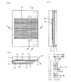
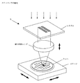
図1は、本発明の実施の形態1に係る液滴吐出ヘッド100の一例を示した模式図である。図1(a)は、液滴吐出ヘッド100の裏面図である。図1(b)は、図1(a)で示した液滴吐出ヘッド100のb−b断面を示す縦断面図である。そして、図1(c)は、図1(a)で示した液滴吐出ヘッド100のc−c断面を示す横断面図である。
Hereinafter, embodiments of the present invention will be described with reference to the drawings.
FIG. 1 is a schematic diagram showing an example of a droplet discharge head 100 according to
図に示した液滴吐出ヘッド100は、ノズル基板の表面側に設けられたノズル孔から液滴を吐出するフェイスイジェクトタイプのものであり、静電気力により駆動される静電駆動方式のものである。また、液滴吐出ヘッド100は、シリコン製のキャビティ基板1を電極基板2とシリコン製のノズル基板3とが上下から挟む構造になっており、キャビティ基板1、電極基板2及びノズル基板3は互いに接合されている。なお、ノズル基板3をシリコン製に限定するものでない。たとえば、ノズル基板3をホウ珪酸ガラス等で形成してもよい。
The droplet discharge head 100 shown in the figure is of a face eject type that discharges droplets from nozzle holes provided on the surface side of a nozzle substrate, and is of an electrostatic drive type that is driven by electrostatic force. . In addition, the droplet discharge head 100 has a structure in which a
ノズル基板3の表面には、多数のノズル穴32が開口している。ノズル基板3とキャビティ基板1との間には、リザーバ11とオリフィス31とを介してリザーバ11に連通している吐出室12が設けられている。この各吐出室12には、ノズル穴32が設けられている。オリフィス31及び吐出室12は、ノズル穴32ごとに個別に設けられている。なお、ノズル穴32は、キャビティ基板1またはノズル基板3に溝を設けて横方向(図1(b)の左方向)からインク液滴を吐出できるように設けてもよい。
A large number of nozzle holes 32 are opened on the surface of the
リザーバ11には、インク供給孔23を介して外部からインクが供給されるようになっている。各吐出室12の底面部分(図1(b)の上側の部分)は、電極ガラス基板2の方向に振動可能な振動板13となっている。電極ガラス基板2のキャビティ基板1との接合面側には、各振動板13に対向する位置に細長い一定の深さの空間部21が設けられている。なお、この空間部21は、電極ガラス基板2に凹部を形成する他に、キャビティ基板1に凹部を形成したり、スペーサを挟むことによって設けることも可能である。
Ink is supplied to the
電極ガラス基板2の空間部21に面する位置には、ITO(Indium Tin Oxide)からなる個別電極22が備えられている。この個別電極22は、一定の間隔の隙間をもって振動板13に対向している。個別電極22は、空間部21の底面に沿って電極ガラス基板2の後端面26まで伸びており、その後端部分が外部配線に接続するための電極取り出し部27となっている。
An
図1に示す液滴吐出ヘッド100は、振動板13と個別電極22との間に電圧を与え、電位差を生じさせることにより、静電気力を発生させて、振動板13を電極ガラス基板2側に湾曲させ、リザーバ11からオリフィス31を介して吐出室12にインクを供給する。そして、振動板13と個別電極22との間に与えた電圧を除去することにより、振動板13が元の状態に復元するように振動してインク液滴をノズル穴32から吐出するようになっている。
The droplet discharge head 100 shown in FIG. 1 applies a voltage between the
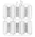
図2〜図5は、液滴吐出ヘッド100の製造工程の一例を示す断面工程図である。図2〜図5に基づいて、液滴吐出ヘッド100の製造工程を詳細に説明する。なお、この液滴吐出ヘッド100の製造方法は、歩留まりが高く、駆動機構(吐出室12、振動板13等)であるアクチュエータが高密度でヘッドサイズがコンパクトな液滴吐出ヘッド100を製造することを目的としている。
2 to 5 are cross-sectional process diagrams illustrating an example of the manufacturing process of the droplet discharge head 100. FIG. The manufacturing process of the droplet discharge head 100 will be described in detail with reference to FIGS. The manufacturing method of the droplet discharge head 100 is to manufacture the droplet discharge head 100 with a high yield, a high density actuator, which is a drive mechanism (
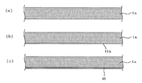
図2は、キャビティ基板1の製造工程を示す断面工程図である。液滴吐出ヘッド100のキャビティ基板1となる下面の研磨された厚さ525μmのSi(シリコン)基板1aを用意する(a)。Si基板1aの研磨された下面(裏側表面)にボロンを高濃度に拡散し、ボロン拡散層13aを形成する(b)。続けて、Si基板1aの下面にプラズマCVD(Chemical Vapor Deposition)装置により絶縁膜43を形成する(c)。この絶縁膜43は、TEOS(TetraEthylOrthoSilicate)からなり、厚さ0.1μmとして形成されている。これは、振動板13の駆動時における絶縁破壊及びショートを防止するため、及びインク等の液滴によるキャビティ基板1のエッチングを防止するためである。
FIG. 2 is a cross-sectional process diagram illustrating the manufacturing process of the
図3は、電極ガラス基板2の製造工程を示す断面工程図である。液滴吐出ヘッド100の電極ガラス基板2となる硼珪酸ガラス製の厚さ1mmのガラス基板2aの上面(表側表面)にCr/Au膜51(クロム・金合金膜)をスパッタにより形成する(a)。次に、フォトリソグラフィーにより空間部21に対応する形状にCr/Au膜51をパターニングし、エッチングによりCr/Au膜51の空間部21に対応する部分を除去する(b)。そして、Cr/Au膜51をエッチングマスクとして、フッ酸水溶液でガラス基板2aをエッチングして空間部21を形成する(c)。なお、フォトリソグラフィーによるパターニングについては後述する(図6、図7参照)。
FIG. 3 is a cross-sectional process diagram illustrating a manufacturing process of the
その後、Cr/Au膜51をエッチングによりすべて除去する(d)。Cr/Au膜51を除去したら、上面全体にITO膜22aをスパッタにより成膜する(e)。次に、フォトリソグラフィーによりITO膜22aに個別電極22に対応する形状をパターニングし、個別電極22となる部分以外のITO膜22aをエッチングにより除去して個別電極22を形成する(f)。そして、インク供給孔を形成する部分をダイヤモンドドリルで穿孔してインク供給孔23を形成する(g)。
Thereafter, all the Cr /
図4及び図5は、Si基板1aとガラス基板2aとを接合する工程及びそれ以降の製造工程を示す断面工程図である。図2の工程で示したボロン拡散層13a及び絶縁膜43を形成したSi基板1aと、図3の工程で示したインク供給孔23を形成したガラス基板2aとを準備する(a)。そして、Si基板1aとガラス基板2aとの間に電圧をかけて陽極接合し、接合基板61を作成する(b)。
4 and 5 are cross-sectional process diagrams illustrating a process of bonding the Si substrate 1a and the
次に、Si基板1aの上面(表側表面)をグラインダーで研削して厚さを約150μmにする。このとき、基板の表面には中心から放物線を描く研削跡が残り、その表面粗さ(Rmax)は0.1μm程度である。続いて、32重量%、80℃の水酸化カリウム水溶液でSi基板1aの上面全体をエッチングし、機械加工(グラインダーで研削)で発生した加工変質層を除去する(c)。このエッチングによってSi基板1a表面は荒れてしまうことになるが、Si基板1aの表面粗さは前述のように1μm以下であることから後工程のノズルプレート接着に問題はない。 Next, the upper surface (front surface) of the Si substrate 1a is ground with a grinder to a thickness of about 150 μm. At this time, a grinding trace drawing a parabola from the center remains on the surface of the substrate, and the surface roughness (Rmax) is about 0.1 μm. Subsequently, the entire upper surface of the Si substrate 1a is etched with a 32 wt% potassium hydroxide aqueous solution at 80 ° C. to remove a work-affected layer generated by machining (grinding with a grinder) (c). Although the surface of the Si substrate 1a is roughened by this etching, since the surface roughness of the Si substrate 1a is 1 μm or less as described above, there is no problem in the subsequent nozzle plate adhesion.
続いて、接合基板61のSi基板1aの表面に、CVD装置によって厚さ1μmのSiO2 膜62(酸化シリコン膜)を形成する(d)。その後、SiO2 膜62の吐出室12に対応する部分12a、リザーバ11に対応する部分11a及び電極取り出し部27に対応する部分27aをフォトリソグラフィーによりパターニングし、これらの部分のSiO2 膜62をエッチングにより除去する(e)。なお、リザーバ11となる部分11aのSiO2 膜62は完全に除去しないようにハーフエッチングする。なお、フォトリソグラフィーによるパターニングについては後述する(図6、図7参照)。
Subsequently, a SiO 2 film 62 (silicon oxide film) having a thickness of 1 μm is formed on the surface of the Si substrate 1a of the
次に、接合基板61を35重量%、80℃の水酸化カリウム水溶液に浸し、吐出室12、電極取り出し部27を途中までエッチングする。そして、リザーバ11に残したフッ酸水溶液でSiO2 膜62を除去し、35重量%、80℃の水酸化カリウム水溶液でエッチングを継続する。こうして、ボロン拡散層13aがエッチングされずに残り、吐出室12の底面のボロン拡散層13aは振動板13となるようになっている。一方、エッチングのスタートを遅らせたリザーバ11は、ボロン拡散層13aまでエッチングが進行せずに、底部となるシリコンを厚く残すことができる(f)。それから、接合基板61をフッ酸水溶液に浸し、Si基板1aの表面に残るSiO2 膜62をすべて除去する(g)。
Next, the
ここまでの工程では、キャビティ基板1と電極ガラス基板2との間に形成された空間部21は完全に密閉されているため、途中工程の処理液が空間部21内(すなわち、アクチュエータ内部)に入り込むということはない。そして、電極取り出し部27に残るボロン拡散層13aと絶縁膜43である薄膜と除去するために、電極取り出し部27に対応する部分27aを開口したメタルマスクをキャビティ基板1に重ねて、ボロン拡散層13aと絶縁膜43をドライエッチングで除去する(h)。
In the steps so far, since the
次に、封止材28を電極取り出し部27の開口部からキャビティ基板1と電極ガラス基板2との間に形成されている空間部21(ギャップ)を塞ぐように塗布し、アクチュエータを封止する(i)。それから、キャビティ基板1の上面(表側表面)にノズル基板3を接合剤でする(j)。最後に、ダイシングして不要な部分除去することで液滴吐出ヘッド100が完成する(k)。
Next, the sealing
次に、本発明に係るパターニング方法について説明する。
図6は、ステッパー5を用いて露光するときの概略を示す説明図である。ステッパー5は、液滴吐出ヘッド100の製造工程で用いられる超微細なパターンを基板に露光・転写するフォトリソグラフィー装置のことである。その基本的な仕組みは、パターンが描かれている写真のネガに相当するレチクルと呼ばれる原版に紫外線等の強い光を当てて、その像を縮小投影レンズを通して超微細に縮小し、感光剤を塗布した写真の印画紙に相当するウエハと呼ばれるシリコン等の基板の表面に、パターンを次々と焼き付けていくものである。このウエハは、平らな台であるステージに載置されている。
Next, the patterning method according to the present invention will be described.
FIG. 6 is an explanatory diagram showing an outline when exposure is performed using the
このステッパー5では、レチクルに描かれたパターニングを約5分の1に縮小することが可能である。また、ステッパー5を用いた露光では、レチクルの描かれたパターンを縮小露光するために、1ショットで露光できるエリアが制限される。たとえば、6インチサイズのレチクルを5分の1に縮小露光する場合、パターン形成される基板(電極ガラス基板2やキャビティ基板1等)の露光可能なエリアは1インチ弱となる(図9参照)。したがって、1チップ分の全部を1ショットで露光することは困難である。
In this
図7は、マスクアライナー6を用いて露光するときの概略を示す説明図である。マスクアライナー6とは、液滴吐出ヘッド100の製造工程で用いられるパターンを基板に露光・転写するフォトリソグラフィー装置のことである。その基本的な仕組みは、ステッパー5と同様であるが、ステッパー5のように縮小露光するのではなく、パターンが描かれている写真のネガに相当するマスクと呼ばれる原版に紫外線等の強い光を当てて、ウエハと呼ばれるシリコン等の基板の表面に、パターンを焼き付けていくものである。ここでは、マスクを例に説明しているが、レチクルであってもよい。
FIG. 7 is an explanatory diagram showing an outline when exposure is performed using the mask aligner 6. The mask aligner 6 is a photolithography apparatus that exposes and transfers a pattern used in the manufacturing process of the droplet discharge head 100 to a substrate. The basic mechanism is the same as that of the
マスクアライナー6を使用すれば、マスクに描かれたパターンを一括で基板に露光することが可能になっている。マスクアライナー6を用いて露光する場合は、ステッパー5を用いて露光する場合に比べて、緻密なパターニングを基板上に形成することができない。すなわち、マスクアライナー6は、必要なマスクの数や露光回数を低減することができるものの、緻密性が要求されるパターン形成(たとえば、吐出室12のパターニング)には適していないのである。
If the mask aligner 6 is used, the pattern drawn on the mask can be exposed to the substrate in a lump. When the exposure is performed using the mask aligner 6, it is not possible to form a dense pattern on the substrate as compared with the case where the exposure is performed using the
図8は、キャビティ基板1となるSi基板1aに形成したSiO2 膜62にパターニングしたときの一部を示す説明図である。ここでは、1つのウエハ(Si基板1a)上で作成する吐出室12(すなわち、アクチュエータ)の数を増やし、1つの液滴吐出ヘッド100に2列の吐出室12を配置して多ノズル化するとともに、ノズル列の長さを1インチとしてチップサイズを大きくした場合を例に説明する。なお、チップサイズが大きくなるに伴って、材料基板(ウエハ)のサイズも大口径化する傾向にある。
FIG. 8 is an explanatory view showing a part when the SiO 2 film 62 formed on the Si substrate 1a to be the
図4(e)で示したように、SiO2 膜62の吐出室12に対応する部分12aやリザーバ11に対応する部分11a、電極取り出し部27に対応する部分27aは、フォトリソグラフィーによりパターニングする。このフォトリソグラフィー装置には、上述したようにステッパー5やマスクアライナー6等の露光装置がある。ステッパー5は、高精度なパターン形成が可能であるが、1ショットで露光できるエリアが限定されている。一方、マスクアライナー6は、1ショットで露光できるエリアは広いが、緻密性が要求されるようなパターン形成には適していない。
As shown in FIG. 4E, the
作成する液滴吐出ヘッド100において、高精度なパターン形成が要求される部分はキャビティ基板1に形成される吐出室12である。したがって、アクチュエータを構成する部分のパターニングを高精度で行わないと、不良品が多く製造されてしまい、歩留まりが低いものとなって作業効率が悪いものとなってしまう。一方、吐出室12以外の部分は、比較的高精度なパターニングが要求されていない。したがって、ステッパー5及びマスクアライナー6双方の利点を有効に利用すれば、コストパフォーマンスの良好な液滴吐出ヘッド100の製造方法を提供することが可能になる。
In the droplet discharge head 100 to be created, a portion that requires highly accurate pattern formation is a
図9は、ステッパー5での1ショット露光が可能なエリアを示す説明図である。図に示すように、ステッパー5を用いた露光では、レチクルのパターンを縮小露光するため、1ショットで露光できるエリアは制限されてしまう。たとえば、6インチサイズのレチクルを使用して、5分の1縮小で露光する場合、キャビティ基板1であるウエハ上で露光可能なエリアは1インチ弱となる。つまり、1ショットで露光可能な範囲は、点線71で示す大きさとなる。したがって、ステッパー5のみでパターニングを実行しようとすると、ショット数が増加し、ステッパー5の負荷が大きくなり、生産性が悪くなるという弊害が生じてしまう。
FIG. 9 is an explanatory diagram showing an area where one-step exposure is possible with the
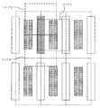
図10は、エリアを分割して露光したパターニングの一例を示す説明図である。図9で示したように、ステッパー5では、液滴吐出ヘッド100の1チップ分のすべてを1ショットで露光することはできない。そのために、図10に示すように、エリアを分割して(ここでは、3つのエリア)露光する必要がある。たとえば、吐出室12の部分であるエリア1、電極取り出し部分27の上部であるエリア2、電極取り出し部27の下部であるエリア3のような範囲を指定して3回露光を行わなければならない。
FIG. 10 is an explanatory diagram illustrating an example of patterning in which an area is divided and exposed. As shown in FIG. 9, the
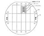
図11は、パターニングされたキャビティ基板1のウエハを示す説明図である。図に示すように、キャビティ基板1のウエハ外周近傍には、ノズル基板3をアライメントするために必要なアライメントマーク91やダイシング時のダイシングマーク95等がパターニングされている。これらをパターニングするためには、それぞれに対してレチクルを作り、その都度露光するしなければならない。ここでも、すべてをステッパー5を用いて露光しようとすると、使用するレチクルの数が増えるとともに、キャビティ基板1全体を露光するためのショット数が増えるため、ステッパへの負荷が大きくなり、生産性が悪くなる。
FIG. 11 is an explanatory view showing a patterned wafer of the
以上のことを考慮して本発明は、高いパターニング精度が要求される吐出室12(エリア1)のみをステッパー5で露光し、吐出室12以外の部分であってあまり高い寸法精度が要求されない部分(エリア2やエリア3)に関しては、キャビティ基板1全体を一括で露光できる大きさのマスクアライナー6で露光するようにした。こうすることで、必要なレチクル数を減らしつつステッパー5での露光ショット数も減らすことができ、全体としての露光工程のスループットが向上する。なお、先にステッパー5で露光し、その後にマスクアライナー6で露光してもよく、先にマスクアライナー6で露光し、その後にステッパー5で露光してもよい。
In consideration of the above, the present invention exposes only the discharge chamber 12 (area 1), which requires high patterning accuracy, with the
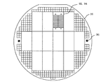
図12は、パターニングされた電極ガラス基板2のウエハを示す説明図である。図に示すように、電極ガラス基板2のウエハ外周近傍には、キャビティ基板1との陽極接合時のアライメントマーク96がパターニングされている。また、その他に、陽極接合界面でのボイド(気泡)発生を防ぐため、接合界面の気体を逃がすための逃げ溝93が形成されている。そして、チップ外周に沿って溝92及びその溝92内に電極94が形成されている。この溝92及び電極94は、各個別電極22の空間部21及び個別電極22と繋がっている。
FIG. 12 is an explanatory diagram showing a patterned
すなわち、チップ内に形成した図示省略の等電位接点で、陽極接合時に振動板13とチップ内で繋がった全ての個別電極22との電位を同じにして、放電による絶縁膜43の破壊を防いでいるのである。ステッパー5で逃げ溝93を形成するためには、電極パターンとは異なるレチクルを複数作製し、それを組み合わせて露光しなければならない。同様に、逃げ溝93を形成するためにも、電極パターンとは異なるレチクルを複数作製し、それを組み合わせて露光しなければならない。したがって、精度が要求される個別電極22の空間部21及び電極パターンはステッパで露光し、チップ外周の溝92、逃げ溝93は基板全体を一括で露光できる大きさのマスクアライナー6で露光することが望ましい。
That is, an equipotential contact (not shown) formed in the chip makes the potential of the
以上説明したように、高いパターニング精度を要求される部分(たとえば、アクチュエータを構成する吐出室12や空間部21等)にはステッパー5を用いて露光を行うため、大口径基板においてもアクチュエータ部を面内均一に高精度にパターニング形成できる。そして、その他の部分をマスクアライナー6で一括して露光を行うため、必要なレチクル数及びその設計工数の削減、ステッパー5露光工程への負荷低減を行い、大口径基板全体における高精度なパターニングを可能としている。実施の形態1では、キャビティ基板1及び電極ガラス基板2におけるパターニングを例に説明したが、これに限定するものではない。たとえば、ステッパー5及びマスクアライナー6を使用するものであれば、適用可能である。
As described above, since exposure is performed using the
実施の形態2.
実施の形態1では、ステッパー5でのパターニングを約5分とマスクアライナーでのパターニングとの順序を特に制限しなかったが、実施の形態2では、ステッパー5でのパターニングを先に実行する場合を例に説明する。上述したように、液滴吐出ヘッド100を製造する際、キャビティ基板1や電極ガラス基板2には、アライメントマーク91やアライメントマーク96、ダイシングマーク95等をパターニングしなければならない。これらは、各基板の重ね合わせがずれないようにしたり、ダイシングする場所を誤らないようにしたりするためにパターン形成されるものである。
In the first embodiment, the order of the patterning by the
これらのマークは、液滴吐出ヘッド100の製造工程の一番最初の工程でパターニングされるのが一般的であり、ステッパー5を用いてパターニングされるようになっている。したがって、これらのマークをパターニングする際に、併せてアクチュエータ部分(キャビティ基板1であれば空間部21、電極ガラス基板2であれば個別電極22)もパターニングすれば、作業工程にかかる手間を省略することができる。
These marks are generally patterned in the very first step of the manufacturing process of the droplet discharge head 100, and are patterned using the
たとえば、これらのマークやアクチュエータ部分を一つのレチクルに描いておけば、レチクル数を低減するとともに、レチクルの交換等にかかる手間を省略することができる。また、これらのマークやアクチュエータ部分を一つのレチクルに描けないときにおいても、パターニングしようとする基板をステッパー5とマスクアライナー6との間で行ったり来たりさせなくて済む。なお、マスクアライナー6で使用するアライメントマークをステッパー5でパターニングすれば、マスクアライナー6での作業工程にかかる手間を省略することができる。
For example, if these marks and actuator portions are drawn on a single reticle, the number of reticles can be reduced and the time and effort required for exchanging reticles can be eliminated. Even when these marks and actuator portions cannot be drawn on one reticle, the substrate to be patterned does not need to be moved back and forth between the
図13は、実施の形態1及び実施の形態2で製造した液滴吐出ヘッド100を搭載した液滴吐出装置150の一例を示した斜視図である。この液滴吐出装置150は、一般的なインクジェットプリンタである。液滴吐出装置150に搭載される液滴吐出ヘッド100は、上述したように電極ガラス基板2やキャビティ基板1のパターニングの際、ステッパー5とマスクアライナー6を適宜使い分けるので、作業効率が良く、高精度なパターニングが実現できるものである。すなわち、液滴吐出ヘッド100は、歩留まりが高く、コストパフォーマンスに優れている製造方法によって製造することができるのである。したがって、この液滴吐出ヘッド100を搭載した液滴吐出装置150も同様な効果を得ることができる。
FIG. 13 is a perspective view showing an example of a
なお、本発明に係る液滴吐出ヘッドの製造方法で得られた液滴吐出ヘッド100は、図13に示したインクジェットプリンタの他に、液滴を種々変更することで、液晶ディスプレイのカラーフィルタの製造、有機EL表示装置の発光部分の形成、生体液体の吐出等にも適用することが可能である。また、本発明の実施の形態に係る液滴吐出ヘッドの製造方法は、本発明の実施の形態に限定されるものではなく、本発明の範囲内において変形可能である。たとえば、静電アクチュエータを用いたマイクロポンプやミラーデバイス等のMEMS(micro Electro Mechanical Systems)デバイスの製造にも応用することができる。 In addition to the inkjet printer shown in FIG. 13, the droplet discharge head 100 obtained by the method for manufacturing a droplet discharge head according to the present invention can be used for various color filters to change the color filter of a liquid crystal display. The present invention can also be applied to production, formation of a light emitting portion of an organic EL display device, discharge of biological liquid, and the like. Further, the manufacturing method of the droplet discharge head according to the embodiment of the present invention is not limited to the embodiment of the present invention, and can be modified within the scope of the present invention. For example, the present invention can also be applied to the manufacture of MEMS (micro Electro Mechanical Systems) devices such as micropumps and mirror devices using electrostatic actuators.
1 キャビティ基板、1a Si基板、2 電極ガラス基板、2a ガラス基板、3 ノズル基板、5 ステッパー、6 マスクアライナー、11 リザーバ、11a リザーバに対応する部分、12 吐出室、12a 吐出室に対応する部分、13 振動板、13a ボロン拡散層、21 空間部(ギャップ)、22 個別電極、22a ITO膜、23 インク供給孔、26 後端面、27 電極取り出し部、27a 電極取り出し部に対応する部分、28 封止剤、31 オリフィス、32 ノズル穴、43 絶縁膜、51 Cr/Au膜、61 接合基板、62 SiO2 膜、71 点線、91 アライメントマーク、92 溝、93 逃げ溝、94 電極、95 ダイシングテープ、96 アライメントマーク、100 液滴吐出ヘッド、150 液滴吐出装置。
1 cavity substrate, 1a Si substrate, 2 electrode glass substrate, 2a glass substrate, 3 nozzle substrate, 5 stepper, 6 mask aligner, 11 reservoir, 11a part corresponding to the reservoir, 12 discharge chamber, 12a part corresponding to the discharge chamber, 13 Diaphragm, 13a Boron diffusion layer, 21 Space part (gap), 22 Individual electrode, 22a ITO film, 23 Ink supply hole, 26 Rear end face, 27 Electrode extraction part, 27a Part corresponding to electrode extraction part, 28 Sealing Agent, 31 Orifice, 32 Nozzle hole, 43 Insulating film, 51 Cr / Au film, 61 Bonding substrate, 62 SiO 2 film, 71 Dotted line, 91 Alignment mark, 92 groove, 93 Escape groove, 94 electrode, 95 Dicing tape, 96 Alignment mark, 100 droplet discharge head, 150 droplet discharge device.
Claims (8)
前記電極ガラス基板に吐出室が形成されるキャビティ基板を、前記電極ガラス基板と前記キャビティ基板との間に空間部となる隙間を隔てて接合する工程と、
前記キャビティ基板をパターニングして少なくとも吐出室を含む液体流路を形成する工程とを有する液滴吐出ヘッドの製造方法において、
前記電極ガラス基板に形成する個別電極に対応する部分のパターニングをステッパーで行い、それ以外の部分のパターニングをマスクアライナーで行う工程と、
前記キャビティ基板に形成する吐出室に対応する部分のパターニングをステッパーで行い、それ以外の部分のパターニングをマスクアライナーで行う工程とを有する
ことを特徴とする液滴吐出ヘッドの製造方法。 Forming an electrode glass substrate including at least individual electrodes by patterning the glass substrate;
Bonding a cavity substrate in which a discharge chamber is formed in the electrode glass substrate with a gap serving as a space between the electrode glass substrate and the cavity substrate;
In the method for manufacturing a droplet discharge head, the method includes patterning the cavity substrate to form a liquid flow path including at least a discharge chamber.
Patterning a portion corresponding to the individual electrode formed on the electrode glass substrate with a stepper, and patterning other portions with a mask aligner; and
And a step of patterning a portion corresponding to the discharge chamber formed on the cavity substrate with a stepper and patterning other portions with a mask aligner. A method of manufacturing a droplet discharge head, comprising:
前記電極ガラス基板に吐出室が形成されるキャビティ基板を、前記電極ガラス基板と前記キャビティ基板との間に空間部となる隙間を隔てて接合する工程と、
前記キャビティ基板をパターニングして少なくとも吐出室を含む液体流路を形成する工程とを有する液滴吐出ヘッドの製造方法において、
はじめに前記電極ガラス基板に形成する個別電極に対応する部分のパターニングをステッパーで行い、その後にそれ以外の部分のパターニングをマスクアライナーで行う工程と、
はじめに前記キャビティ基板に形成する吐出室に対応する部分のパターニングをステッパーで行い、その後にそれ以外の部分のパターニングをマスクアライナーで行う工程とを有する
ことを特徴とする液滴吐出ヘッドの製造方法。 Patterning the glass substrate to form an electrode glass substrate including at least individual electrodes;
Bonding a cavity substrate in which a discharge chamber is formed in the electrode glass substrate with a gap serving as a space between the electrode glass substrate and the cavity substrate;
In the method for manufacturing a droplet discharge head, the method includes patterning the cavity substrate to form a liquid flow path including at least a discharge chamber.
First, patterning a portion corresponding to the individual electrode to be formed on the electrode glass substrate with a stepper, and then patterning the other portion with a mask aligner,
First, patterning a portion corresponding to the discharge chamber formed on the cavity substrate with a stepper and then patterning the other portion with a mask aligner.
前記電極ガラス基板と前記キャビティ基板とを位置合わせするためのアライメントマークに対応する部分のパターニングを前記工程で併せて行う
ことを特徴とする請求項1または2に記載の液滴吐出ヘッドの製造方法。 In the process of patterning the glass substrate to form an electrode glass substrate including at least individual electrodes,
The method for manufacturing a droplet discharge head according to claim 1, wherein patterning of a portion corresponding to an alignment mark for aligning the electrode glass substrate and the cavity substrate is performed in the step. .
前記電極ガラス基板と前記キャビティ基板とを位置合わせするためのアライメントマークに対応する部分のパターニングを前記工程で併せて行う
ことを特徴とする請求項1または2に記載の液滴吐出ヘッドの製造方法。 In the step of patterning the cavity substrate to form a liquid flow path including at least the discharge chamber,
The method for manufacturing a droplet discharge head according to claim 1, wherein patterning of a portion corresponding to an alignment mark for aligning the electrode glass substrate and the cavity substrate is performed in the step. .
ことを特徴とする請求項3または4に記載の液滴吐出ヘッドの製造方法。 The method for manufacturing a droplet discharge head according to claim 3, wherein patterning of a portion corresponding to the alignment mark is performed by a stepper.
前記個別電極及び該電極ガラス基板に形成するアライメントマークに対応する部分のパターニングをステッパーを用いて同時に行う
ことを特徴とする請求項3または5に記載の液滴吐出ヘッドの製造方法。 In the process of patterning the glass substrate to form an electrode glass substrate including at least individual electrodes,
6. The method of manufacturing a droplet discharge head according to claim 3, wherein patterning of the individual electrodes and portions corresponding to the alignment marks formed on the electrode glass substrate is simultaneously performed using a stepper.
前記吐出室及び該キャビティ基板に形成するアライメントマークに対応する部分のパターニングをステッパーを用いて同時に行う
ことを特徴とする請求項4または5に記載の液滴吐出ヘッドの製造方法。 In the step of patterning the cavity substrate to form a liquid flow path including at least the discharge chamber,
6. The method of manufacturing a droplet discharge head according to claim 4, wherein patterning of the discharge chamber and a portion corresponding to an alignment mark formed on the cavity substrate is simultaneously performed using a stepper.
ことを特徴とする液滴吐出装置の製造方法。
A method for manufacturing a droplet discharge device, comprising the method for manufacturing a droplet discharge head according to claim 1.
Priority Applications (1)
| Application Number | Priority Date | Filing Date | Title |
|---|---|---|---|
| JP2005245153A JP2007055152A (en) | 2005-08-26 | 2005-08-26 | Method for manufacturing droplet discharge head and method for manufacturing droplet discharge device |
Applications Claiming Priority (1)
| Application Number | Priority Date | Filing Date | Title |
|---|---|---|---|
| JP2005245153A JP2007055152A (en) | 2005-08-26 | 2005-08-26 | Method for manufacturing droplet discharge head and method for manufacturing droplet discharge device |
Publications (1)
| Publication Number | Publication Date |
|---|---|
| JP2007055152A true JP2007055152A (en) | 2007-03-08 |
Family
ID=37919036
Family Applications (1)
| Application Number | Title | Priority Date | Filing Date |
|---|---|---|---|
| JP2005245153A Withdrawn JP2007055152A (en) | 2005-08-26 | 2005-08-26 | Method for manufacturing droplet discharge head and method for manufacturing droplet discharge device |
Country Status (1)
| Country | Link |
|---|---|
| JP (1) | JP2007055152A (en) |
Cited By (3)
| Publication number | Priority date | Publication date | Assignee | Title |
|---|---|---|---|---|
| JP2014133384A (en) * | 2013-01-11 | 2014-07-24 | Canon Inc | Method for manufacturing liquid discharge head |
| JP2014148163A (en) * | 2013-01-11 | 2014-08-21 | Canon Inc | Process for producing chip |
| JP2020090082A (en) * | 2018-12-07 | 2020-06-11 | チェン ファ コーティング テクノロジー,インコーポレイテッド | Method for manufacturing thermal print head |
-
2005
- 2005-08-26 JP JP2005245153A patent/JP2007055152A/en not_active Withdrawn
Cited By (5)
| Publication number | Priority date | Publication date | Assignee | Title |
|---|---|---|---|---|
| JP2014133384A (en) * | 2013-01-11 | 2014-07-24 | Canon Inc | Method for manufacturing liquid discharge head |
| JP2014148163A (en) * | 2013-01-11 | 2014-08-21 | Canon Inc | Process for producing chip |
| JP2020090082A (en) * | 2018-12-07 | 2020-06-11 | チェン ファ コーティング テクノロジー,インコーポレイテッド | Method for manufacturing thermal print head |
| KR20200070966A (en) * | 2018-12-07 | 2020-06-18 | 치엔 화 코팅 테크놀로지, 인코포레이티드 | Method for manufacturing thermal print head |
| KR102190615B1 (en) * | 2018-12-07 | 2020-12-16 | 치엔 화 코팅 테크놀로지, 인코포레이티드 | Method for manufacturing thermal print head |
Similar Documents
| Publication | Publication Date | Title |
|---|---|---|
| KR101690893B1 (en) | Nozzle plate, method of manufacturing nozzle plate, inkjet head, and inkjet printing apparatus | |
| KR100465444B1 (en) | Narrow-pitch connector, electrostatic actuator, piezoelectric actuator, ink-jet head, ink-jet printer, micromachine, liquid crystal panel, and electronic apparatus | |
| CN111216452B (en) | Piezoelectric type MEMS ink-jet printing head and manufacturing method | |
| JP2012025146A (en) | Ink jet print head and method for manufacturing the same | |
| JP2007055152A (en) | Method for manufacturing droplet discharge head and method for manufacturing droplet discharge device | |
| JP4333724B2 (en) | Droplet discharge head, droplet discharge device, method for manufacturing droplet discharge head, and method for manufacturing droplet discharge device | |
| JP2008273036A (en) | Nozzle substrate manufacturing method, droplet discharge head manufacturing method, and droplet discharge apparatus manufacturing method | |
| US20060261035A1 (en) | Liquid discharge head and producing method therefor | |
| JP2009073072A (en) | Method for manufacturing droplet discharge head and method for manufacturing droplet discharge device | |
| KR101179320B1 (en) | Method for manufacturing inkjet head | |
| JP2006256222A (en) | Electrostatic actuator, electrostatic actuator manufacturing method, droplet discharge head, droplet discharge head manufacturing method, droplet discharge apparatus, droplet discharge apparatus manufacturing method, device, and device manufacturing method | |
| JP2008132733A (en) | Droplet discharge head, droplet discharge apparatus, and method of manufacturing droplet discharge head | |
| JP5728947B2 (en) | Alignment mark forming method, nozzle substrate forming method, nozzle substrate and droplet discharge head | |
| JP2007276307A (en) | Droplet discharge head, droplet discharge device, method for manufacturing droplet discharge head, and method for manufacturing droplet discharge device | |
| JP2007001297A (en) | Liquid discharge head and manufacturing method thereof | |
| JP2007001296A (en) | Liquid discharge head and manufacturing method thereof | |
| JP4645631B2 (en) | Droplet discharge head, droplet discharge device, method for manufacturing droplet discharge head, and method for manufacturing droplet discharge device | |
| JP2006308842A (en) | Pattern transfer method, electronic device manufacturing method, and liquid ejecting apparatus | |
| JP2007083464A (en) | Mask, mask manufacturing method, droplet discharge head manufacturing method, and droplet discharge apparatus manufacturing method | |
| JP2007021839A (en) | Droplet discharge head, manufacturing method thereof, and droplet discharge apparatus | |
| JP4696836B2 (en) | Electrostatic actuator manufacturing method and electrostatic actuator | |
| JP2009067025A (en) | Ink jet head and method of manufacturing ink jet head | |
| JP2006159587A (en) | Protective jig, method of using the same, method of manufacturing droplet discharge head using the protective jig, droplet discharge head manufactured by the method, and droplet discharge apparatus equipped with the droplet discharge head | |
| JP2008062414A (en) | Manufacturing method for inkjet head | |
| JP2005212294A (en) | Electrostatic actuator manufacturing method, droplet discharge head manufacturing method, electrostatic actuator, droplet discharge head, and droplet discharge apparatus |
Legal Events
| Date | Code | Title | Description |
|---|---|---|---|
| A300 | Withdrawal of application because of no request for examination |
Free format text: JAPANESE INTERMEDIATE CODE: A300 Effective date: 20081104 |