JP5714817B2 - Probe card - Google Patents
Probe card Download PDFInfo
- Publication number
- JP5714817B2 JP5714817B2 JP2009523661A JP2009523661A JP5714817B2 JP 5714817 B2 JP5714817 B2 JP 5714817B2 JP 2009523661 A JP2009523661 A JP 2009523661A JP 2009523661 A JP2009523661 A JP 2009523661A JP 5714817 B2 JP5714817 B2 JP 5714817B2
- Authority
- JP
- Japan
- Prior art keywords
- interposer
- wiring board
- probe card
- probe
- wiring
- Prior art date
- Legal status (The legal status is an assumption and is not a legal conclusion. Google has not performed a legal analysis and makes no representation as to the accuracy of the status listed.)
- Expired - Fee Related
Links
Images


Classifications
-
- G—PHYSICS
- G01—MEASURING; TESTING
- G01R—MEASURING ELECTRIC VARIABLES; MEASURING MAGNETIC VARIABLES
- G01R31/00—Arrangements for testing electric properties; Arrangements for locating electric faults; Arrangements for electrical testing characterised by what is being tested not provided for elsewhere
- G01R31/28—Testing of electronic circuits, e.g. by signal tracer
- G01R31/2851—Testing of integrated circuits [IC]
- G01R31/2886—Features relating to contacting the IC under test, e.g. probe heads; chucks
- G01R31/2891—Features relating to contacting the IC under test, e.g. probe heads; chucks related to sensing or controlling of force, position, temperature
-
- G—PHYSICS
- G01—MEASURING; TESTING
- G01R—MEASURING ELECTRIC VARIABLES; MEASURING MAGNETIC VARIABLES
- G01R1/00—Details of instruments or arrangements of the types included in groups G01R5/00 - G01R13/00 and G01R31/00
- G01R1/02—General constructional details
- G01R1/06—Measuring leads; Measuring probes
- G01R1/067—Measuring probes
- G01R1/06711—Probe needles; Cantilever beams; "Bump" contacts; Replaceable probe pins
- G01R1/06716—Elastic
- G01R1/06722—Spring-loaded
-
- G—PHYSICS
- G01—MEASURING; TESTING
- G01R—MEASURING ELECTRIC VARIABLES; MEASURING MAGNETIC VARIABLES
- G01R1/00—Details of instruments or arrangements of the types included in groups G01R5/00 - G01R13/00 and G01R31/00
- G01R1/02—General constructional details
- G01R1/06—Measuring leads; Measuring probes
- G01R1/067—Measuring probes
- G01R1/073—Multiple probes
- G01R1/07307—Multiple probes with individual probe elements, e.g. needles, cantilever beams or bump contacts, fixed in relation to each other, e.g. bed of nails fixture or probe card
- G01R1/07364—Multiple probes with individual probe elements, e.g. needles, cantilever beams or bump contacts, fixed in relation to each other, e.g. bed of nails fixture or probe card with provisions for altering position, number or connection of probe tips; Adapting to differences in pitch
- G01R1/07371—Multiple probes with individual probe elements, e.g. needles, cantilever beams or bump contacts, fixed in relation to each other, e.g. bed of nails fixture or probe card with provisions for altering position, number or connection of probe tips; Adapting to differences in pitch using an intermediate card or back card with apertures through which the probes pass
Description
本発明は、検査対象である半導体ウェハと検査用の信号を生成する回路構造との間を電気的に接続するプローブカードに関する。 The present invention relates to a probe card for electrically connecting a semiconductor wafer to be inspected and a circuit structure for generating an inspection signal.
半導体の検査工程では、ダイシングする前の半導体ウェハの状態で導電性を有するプローブ(導電性接触子)をコンタクトさせることによって導通検査等の電気特性検査を行い、不良品を検出する(ウェハレベルテスト)。このウェハレベルテストを行う際には、検査用の信号を半導体ウェハへ伝送するために、多数のプローブを収容するプローブカードが用いられる。ウェハレベルテストでは、半導体ウェハ上のダイをプローブカードでスキャニングしながらプローブをダイごとに個別にコンタクトさせるが、半導体ウェハ上には数百〜数万というダイが形成されているので、一つの半導体ウェハをテストするにはかなりの時間を要し、ダイの数が増加するとともにコストの上昇を招いていた。 In the semiconductor inspection process, electrical characteristics inspection such as continuity inspection is performed by contacting a conductive probe (conductive contactor) in the state of the semiconductor wafer before dicing to detect defective products (wafer level test). ). When performing this wafer level test, a probe card containing a large number of probes is used to transmit inspection signals to the semiconductor wafer. In the wafer level test, the probe is contacted individually for each die while scanning the die on the semiconductor wafer with a probe card, but hundreds to tens of thousands of dies are formed on the semiconductor wafer, so one semiconductor It took a considerable amount of time to test the wafer, increasing the number of dies and increasing the cost.
上述したウェハレベルテストの問題点を解消するために、最近では、半導体ウェハ上の全てのダイ、または半導体ウェハ上の少なくとも1/4〜1/2程度のダイに数百〜数万のプローブを一括してコンタクトさせるフルウェハレベルテストという手法も用いられている(例えば、特許文献1を参照)。この手法では、プローブを半導体ウェハ上の電極パッドに対して正確にコンタクトさせるため、半導体ウェハの表面に対するプローブカードの平行度や平面度を精度よく保つことによってプローブの先端位置精度を保持する技術や、半導体ウェハを高精度でアライメントする技術が知られている(例えば、特許文献2または3を参照)。
In order to solve the problems of the wafer level test described above, several hundred to several tens of thousands of probes have been recently installed on all the dies on the semiconductor wafer or at least about ¼ to ½ of the dies on the semiconductor wafer. A technique called a full wafer level test in which contact is made at once is also used (see, for example, Patent Document 1). In this method, in order to accurately contact the probe with the electrode pad on the semiconductor wafer, a technique for maintaining the probe tip position accuracy by accurately maintaining the parallelism and flatness of the probe card with respect to the surface of the semiconductor wafer, A technique for aligning semiconductor wafers with high accuracy is known (see, for example,
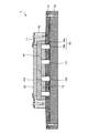
図11は、上述したフルウェハレベルテストにおいて適用されるプローブカードの構成を示す部分断面図である。同図に示すプローブカード9は、半導体ウェハ上の電極パッドの配置パターンに対応して設けられた複数のプローブ10を収容するプローブヘッド91と、プローブヘッド91における微細な配線パターンの間隔を変換するスペーストランスフォーマ92と、スペーストランスフォーマ92から出た配線wを中継するインターポーザ93と、インターポーザ93が中継した配線を検査装置へ接続する配線基板94と、配線基板94に設けられて検査装置側のメスコネクタに接続されるオスコネクタ95と、配線基板94を補強する補強部材96と、を備える。
FIG. 11 is a partial cross-sectional view showing a configuration of a probe card applied in the above-described full wafer level test. The probe card 9 shown in the figure converts a
このうち、インターポーザ93としては、絶縁性材料から成る薄膜状の基材と、この基材の両面に所定のパターンで配設され、片持ち梁状をなす板ばね式の複数の接続端子とを有するものが知られている。この場合には、インターポーザ93の一方の表面に設けられた接続端子がスペーストランスフォーマ92の電極パッドに接触するとともに、他方の表面に設けられた接続端子が配線基板94の電極パッドに接触することによって両者の電気的な接続を図っている。
Among these, as the
しかしながら、プローブカード9のような従来のプローブカードをフルウェハレベルテストに適用する場合には、配線基板の径が8〜12インチ(約200〜300mm)程度と大きくなるため、配線基板が反りや波打ち等の変形を起こしやすく、所定の基準面に対するプローブヘッドの平行度の精度やプローブヘッドの平面度の精度を低下させる要因となっていた。 However, when a conventional probe card such as the probe card 9 is applied to a full wafer level test, the diameter of the wiring board becomes as large as about 8 to 12 inches (about 200 to 300 mm). Deformation such as undulation is likely to occur, and this is a factor that decreases the accuracy of the parallelism of the probe head with respect to a predetermined reference surface and the accuracy of the flatness of the probe head.
また、従来のプローブカードでは、スペーストランスフォーマがインターポーザから弾性力を受けることによって反りを生じた場合、プローブヘッドもスペーストランスフォーマに追従して反りを生じるため、配線基板が変形した場合と同様、所定の基準面に対するプローブヘッドの平行度の精度やプローブヘッドの平面度の精度が低下させることがあった。 Further, in the conventional probe card, when the space transformer is warped by receiving an elastic force from the interposer, the probe head also warps following the space transformer. The accuracy of the parallelism of the probe head with respect to the reference surface and the accuracy of the flatness of the probe head may be reduced.
本発明は、上記に鑑みてなされたものであって、異なる回路構造間で電気信号の入出力を行うプローブを収容するプローブヘッドの所定の基準面に対する平行度の精度や平面度の精度を向上させることができるプローブカードを提供することを目的とする。 The present invention has been made in view of the above, and improves the accuracy of parallelism and flatness with respect to a predetermined reference plane of a probe head that houses a probe that inputs and outputs electrical signals between different circuit structures. It is an object of the present invention to provide a probe card that can be used.
上述した課題を解決し、目的を達成するために、本発明に係るプローブカードは、各々が導電性材料からなり、長手方向に沿って弾性力による伸縮を行う複数のプローブを用いることにより、半導体ウェハと当該半導体ウェハに対して出力する信号を生成する回路構造との電気的な接続を確立するプローブカードであって、前記複数のプローブを保持するプローブヘッドと、前記回路構造に対応する配線パターンを有する配線基板と、前記配線基板に積層され、前記配線基板の配線を中継する平板状のインターポーザと、前記インターポーザと前記プローブヘッドとの間に介在し、前記インターポーザが中継する配線の間隔を変換し、この変換した配線を前記プローブヘッドと対向する表面に表出する平板状のスペーストランスフォーマと、前記配線基板の板厚と前記インターポーザの板厚との和よりも大きい高さを有する略柱状をなし、前記配線基板および前記インターポーザを板厚方向に貫通して埋め込まれ、一方の底面が前記スペーストランスフォーマに当接する複数のポスト部材と、を備えたことを特徴とする。 In order to solve the above-described problems and achieve the object, the probe card according to the present invention includes a plurality of probes each made of a conductive material and extending and contracting by an elastic force along the longitudinal direction. A probe card that establishes an electrical connection between a wafer and a circuit structure that generates a signal to be output to the semiconductor wafer, a probe head that holds the plurality of probes, and a wiring pattern corresponding to the circuit structure The interposer is disposed between the interposer and the probe head, and the interval between the wirings relayed by the interposer is converted. A flat space transformer that exposes the converted wiring on the surface facing the probe head; A substantially columnar shape having a height greater than the sum of the thickness of the wiring board and the thickness of the interposer, embedded through the wiring board and the interposer in the thickness direction, and one bottom surface is the space And a plurality of post members in contact with the transformer.
また、本発明に係るプローブカードは、上記発明において、前記インターポーザと前記スペーストランスフォーマは固着されていることを特徴とする。 In the probe card according to the present invention, the interposer and the space transformer are fixed to each other.
また、本発明に係るプローブカードは、上記発明において、前記インターポーザは、各々が導電性材料からなり、長手方向に沿って弾性力による伸縮を行う複数の接続端子と、平板状の絶縁性材料からなり、前記複数の接続端子の各々を個別に収容する複数の貫通孔部が形成されたハウジング部材と、を有し、各接続端子の長手方向の両端部は、前記ハウジング部材から露出していることを特徴とする。 In the probe card according to the present invention, in the above invention, each of the interposers is made of a conductive material, and includes a plurality of connection terminals that extend and contract by elastic force along the longitudinal direction, and a flat insulating material. A plurality of through holes that individually accommodate each of the plurality of connection terminals, and both end portions in the longitudinal direction of the connection terminals are exposed from the housing member. It is characterized by that.
また、本発明に係るプローブカードは、上記発明において、前記配線基板に装着され、前記配線基板を補強する補強部材をさらに備え、前記複数のポスト部材は、前記補強部材に固着されていることを特徴とする。 The probe card according to the present invention may further include a reinforcing member that is attached to the wiring board and reinforces the wiring board, and the plurality of post members are fixed to the reinforcing member. Features.
本発明に係るプローブカードによれば、配線基板の板厚とインターポーザの板厚との和よりも大きい高さを有する略柱状をなし、配線基板およびインターポーザを板厚方向に貫通して埋め込まれ、一方の底面がスペーストランスフォーマに当接する複数のポスト部材を備えたことにより、異なる回路構造間で電気信号の入出力を行うプローブを収容するプローブヘッドの所定の基準面に対する平行度の精度や平面度の精度を向上させることが可能となる。 The probe card according to the present invention has a substantially columnar shape having a height larger than the sum of the thickness of the wiring board and the thickness of the interposer, and is embedded through the wiring board and the interposer in the thickness direction. By providing a plurality of post members whose one bottom surface abuts against the space transformer, the accuracy and flatness of the parallelism with respect to a predetermined reference plane of a probe head that accommodates probes for inputting and outputting electric signals between different circuit structures It is possible to improve the accuracy.
1、6、7、8、9 プローブカード
2、10 プローブ
3 プローバ
4 コネクタ座
5 半導体ウェハ
11、61、94 配線基板
12、62、82、96 補強部材
13、63、93 インターポーザ
14、92 スペーストランスフォーマ
15、91 プローブヘッド
15p プローブ収容領域
16 保持部材
17 リーフスプリング
18、83 ポスト部材
18a、83a 大径部
18b、83b 小径部
71 接着剤
20、95 オスコネクタ
21、22 プランジャ
21a、22a、134a、135a 先端部
21b、134c、135c ボス部
21c 軸部
22b、134b、135b フランジ部
22c、134d、135d 基端部
23、136 バネ部材
23a、136a 粗巻き部
23b、136b 密着巻き部
31 プローブカードホルダ
32 押え治具
40 メスコネクタ
50 ウェハチャック
51、112、141、142 電極パッド
84 ナット
111、131、137、138、151、611、821 貫通孔部
121 外周部
122 中心部
123 連結部
124、624 凹部
132 ハウジング部材
132a 第1部材
132b 第2部材
133 接続端子
134、135 プランジャ
137a、138a、151a、821a 小径孔
137b、138b、151b、821b 大径孔
171 爪部
w 配線
DESCRIPTION OF
以下、添付図面を参照して本発明を実施するための最良の形態(以後、「実施の形態」と称する)を説明する。なお、図面は模式的なものであって、各部分の厚みと幅との関係、それぞれの部分の厚みの比率などは現実のものとは異なる場合もあることに留意すべきであり、図面の相互間においても互いの寸法の関係や比率が異なる部分が含まれる場合があることは勿論である。 The best mode for carrying out the present invention (hereinafter referred to as “embodiment”) will be described below with reference to the accompanying drawings. It should be noted that the drawings are schematic, and the relationship between the thickness and width of each part, the ratio of the thickness of each part, and the like may be different from the actual ones. Of course, there may be included portions having different dimensional relationships and ratios.
(実施の形態1)
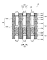
図1は、本発明の実施の形態1に係るプローブカードの構成を示す分解斜視図である。図2は、本実施の形態1に係るプローブカードの平面図である。図3は、図2のA−A線部分断面図である。図4は、図2のB−B線断面を配線の一部も含めて模式的に示す図であり、本実施の形態1に係るプローブカードを用いた電気特性検査の概要を示す図である。なお、図4では、実際の検査時と上下を一致させるため、図3とプローブカード1の上下を逆転させている。これらの図1〜図4に示すプローブカード1は、検査対象である半導体ウェハ5と検査用の信号を生成する回路構造を具備した検査装置とを電気的に接続する装置である。(Embodiment 1)
FIG. 1 is an exploded perspective view showing a configuration of a probe card according to
プローブカード1は、円盤状をなし、検査装置との電気的な接続を図る配線基板11と、配線基板11の一方の面に装着され、配線基板11を補強する補強部材12と、配線基板11からの配線を中継するインターポーザ13と、インターポーザ13によって中継された配線の間隔を変換するスペーストランスフォーマ14と、配線基板11よりも径が小さい円盤状をなしてスペーストランスフォーマ14に積層され、検査対象の半導体ウェハ5の配線パターンに対応して複数のプローブ2を収容保持するプローブヘッド15と、配線基板11に固着され、インターポーザ13およびスペーストランスフォーマ14を積層した状態で一括して保持する保持部材16と、保持部材16に固着されてプローブヘッド15の端部を固定するリーフスプリング17と、配線基板11およびインターポーザ13を板厚方向に貫通して埋め込まれる複数のポスト部材18と、を備える。
The
配線基板11は、ベークライトやエポキシ樹脂等の絶縁性材料を用いて形成され、複数のプローブ2と検査装置とを電気的に接続するための配線層がビアホール等によって立体的に形成されている。配線基板11は、板厚方向に貫通された複数の貫通孔部111を有する。なお、図3においては、本来平板状である配線基板11が変形し、その配線基板11の縦断面が波打っている状態を示している。
The
図4に示すように、配線基板11に形成される配線wの一端は、検査装置(図示せず)との接続を行うために配線基板11の表面であって補強部材12が装着された側の表面に配設された複数のオスコネクタ20に接続される。これに対して、配線wの他端は、スペーストランスフォーマ14を介してプローブヘッド15で収容保持するプローブ2に電気的に接続されている。
As shown in FIG. 4, one end of the wiring w formed on the
各オスコネクタ20は、配線基板11の中心に対して放射状に配設され、検査装置のコネクタ座4で対向する位置に設けられるメスコネクタ40の各々と対をなし、互いの端子が接触することによってプローブ2と検査装置との電気的な接続を確立する。オスコネクタ20およびメスコネクタ40から構成されるコネクタとして、オスコネクタを挿抜する際に外力をほとんど必要とせず、コネクタ同士を結合した後に外力によって圧接力を加えるゼロインサーションフォース(ZIF)型コネクタを適用することができる。このZIF型コネクタを適用すれば、プローブカード1や検査装置は、プローブ2の数が多くても接続によるストレスをほとんど受けずに済むため、電気的な接続を確実に得ることができることに加え、プローブカード1の耐久性を向上させることもできる。
Each
なお、配線基板11にメスコネクタを配設する一方、コネクタ座4にオスコネクタを配設してもよい。また、コネクタの代わりに、スプリング作用のあるポゴピン等の端子を検査装置に設け、その端子を介してプローブカード1を検査装置に接続する構成としてもよい。
A female connector may be provided on the
補強部材12は、図1に示すように、配線基板11と略同径を有する円形の外周部121と、外周部121のなす円と同じ中心を有し、インターポーザ13の表面よりも若干表面積が大きい円盤状をなす中心部122と、中心部122の外周方向から外周部121に達するまで延出し、外周部121と中心部122とを連結する複数の連結部123とを備える。また、補強部材12の中心部122には、ポスト部材18の端部(後述する小径部18b)を載置する凹部124が複数個形成されている。補強部材12は、アルマイト仕上げを行ったアルミニウム、ステンレス、インバー材、コバール材(登録商標)、ジュラルミンなど剛性の高い材料によって実現される。
As shown in FIG. 1, the reinforcing
インターポーザ13は、正8角形の表面を有し、薄板状をなす。インターポーザ13には、板厚方向に貫通され、配線基板11の貫通孔部111と同じ径を有する複数の貫通孔部131が設けられている。各貫通孔部131は、配線基板11に積層された状態で、配線基板11が有する複数の貫通孔部111のいずれかと連通している。
The
図5は、インターポーザ13の詳細な内部構成を示す拡大部分断面図である。図5に示すように、インターポーザ13は、ハウジング部材132に複数の接続端子133が収容保持されて成る。接続端子133は、配線基板11と接触するプランジャ134と、スペーストランスフォーマ14と接触するプランジャ135と、プランジャ134、135の間に設けられてプランジャ134、135を伸縮自在に連結するコイル状のバネ部材136とを備える。互いに連結されるプランジャ134、135、およびバネ部材136は同一の軸線を有している。
FIG. 5 is an enlarged partial sectional view showing a detailed internal configuration of the
プランジャ134は、先鋭端を有する先端部134aと、先端部134aの径よりも大きい径を有するフランジ部134bと、フランジ部134bを介して先端部134aと反対方向に突出し、フランジ部134bの径よりも小さくかつバネ部材136の内径よりも若干大きい径の円柱状をなし、バネ部材23の端部が圧入されるボス部134cと、ボス部134cの径よりも小さくかつバネ部材136の内径よりも小さい径の円柱状をなし、ボス部134cからフランジ部134bと反対側に延在する基端部134dと、を有し、長手方向の中心軸に対して軸対称な形状をなしている。
The
プランジャ135は、複数の爪が突出したクラウン形状をなす先端部135aと、先端部135aの径よりも大きい径を有するフランジ部135bと、フランジ部135bを介して先端部135aと反対方向に突出し、フランジ部135bの径よりも小さくかつバネ部材136の内径よりも若干大きい径の円柱状をなし、バネ部材136の端部が圧入されるボス部135cと、ボス部135cの径よりも小さくかつバネ部材136の内径よりも小さい径の円柱状をなし、ボス部135cからフランジ部135bと反対側に延在する基端部135dと、を有し、長手方向の中心軸に対して軸対称な形状をなしている。フランジ部135bの径はフランジ部134bの径と同じであり基端部135dの径は基端部134dの径と同じである。
The
バネ部材136は、プランジャ134に取り付けられる側が粗巻き部136aである一方、プランジャ135に取り付けられる側が密着巻き部136bである。粗巻き部136aの端部はフランジ部134bに当接する一方、密着巻き部136bの端部はフランジ部135bに当接している。
In the
接続端子133を収容するハウジング部材132は、第1部材132aと第2部材132bとが重ね合わさって成る。第1部材132aには、複数の接続端子133を個別に収容する貫通孔部137が形成されている。貫通孔部137は、先端部134aの径よりも若干大きい径を有する小径孔137aと、フランジ部134bよりも若干大きい径を有する大径孔137bとを備え、これら小径孔137aおよび大径孔137bが同じ軸線を有する段付き孔形状をなす。一方、第2部材132bには、複数の接続端子133を個別に収容する貫通孔部138が形成されている。貫通孔部138は貫通孔部137と連通しており、先端部135aの径よりも若干大きい径を有する小径孔138aと、フランジ部135bよりも若干大きい径を有する大径孔138bとを備え、これら小径孔138aおよび大径孔138bが同じ軸線を有する段付き孔形状をなす。貫通孔部137、138の各々は、貫通孔部131の一部をなしている。
The
図5において、プランジャ134は、フランジ部134bが第1部材132aの貫通孔部137の大径孔137bと小径孔137aとの境界をなす段差部分に当接することによってハウジング部材132からの抜け止めされている。同様に、プランジャ135は、フランジ部135bが第2部材132bの貫通孔部138の小径孔138aと大径孔138bとの境界をなす段差部分に当接することによってハウジング部材132からの抜け止めされている。
In FIG. 5, the
図6は、プローブカード1のインターポーザ13周辺の構成を示す図である。同図に示すインターポーザ13は、配線基板11とスペーストランスフォーマ14との間に介在し、プランジャ134の先端が配線基板11の電極パッド112に接触する一方、プランジャ135の先端がスペーストランスフォーマ14の電極パッド141に接触することにより、配線基板11とスペーストランスフォーマ14との電気的な接続を中継している。
FIG. 6 is a diagram showing a configuration around the
図6において、バネ部材136は湾曲して密着巻き部136bの一部がプランジャ134の基端部134dに接触している。これにより、プランジャ134、バネ部材136の密着巻き部136bおよびプランジャ135を順次経由する最短経路の電気導通が実現され、接続端子133のインダクタンスの増加が抑制されている。
In FIG. 6, the
以上の構成を有するインターポーザ13は、各々の接続端子133が独立に伸縮することができるため、配線基板11やスペーストランスフォーマ14の変形にインターポーザ13を追従させることができる。この結果、配線基板11および/またはスペーストランスフォーマ14の変形によって一部の配線が断線してしまうのを防止することができるとともに、半導体ウェハ5の熱膨張係数と配線基板11の熱膨張係数との差を吸収することができる。
In the
なお、インターポーザ13に適用される接続端子133のプランジャ134、135は互いに異なる形状をなしているが、互いに同じ形状を有するプランジャをバネ部材136によって接続してもよい。また、プランジャ134とプランジャ135を上下逆に配置してもよい。
Although the
スペーストランスフォーマ14は、セラミックス等の絶縁性材料を母材とし、配線基板11と同様、内部の配線層がビアホール等によって立体的に形成されている。スペーストランスフォーマ14はインターポーザ13と略合同な正8角形の表面を有し、薄板状をなしている。
The
図7は、プローブヘッド15要部の構成およびプローブ2の詳細な構成を示す拡大部分断面図である。プローブ2は、スペーストランスフォーマ14と接触するプランジャ21と、プランジャ21と相反する向きに突出し、半導体ウェハ5の電極パッド51に接触するプランジャ22と、プランジャ21、22の間に設けられ、プランジャ21、22を伸縮自在に連結するコイル状のバネ部材23とを備える。互いに連結されるプランジャ21、22、およびバネ部材23は同一の軸線を有している。
FIG. 7 is an enlarged partial sectional view showing the configuration of the main part of the
プランジャ21は、先鋭端を有する先端部21aと、先端部21aの基端側に設けられ、先端部21aの径よりも小さい径を有するボス部21bと、ボス部21bの表面のうち先端部21aと接する側と反対側の表面から延出する軸部21cとを備える。一方、プランジャ22は、先鋭端を有する先端部22aと、先端部22aの基端側に設けられ、先端部22aの径よりも大きい径を有するフランジ部22bと、フランジ部22bの表面から先端部22aと相反する方向へ突出し、フランジ部22bの径よりも小さい径を有するボス状の基端部22cとを有する。
The
バネ部材23は、プランジャ21に取り付けられる側が粗巻き部23aである一方、プランジャ22に取り付けられる側が密着巻き部23bである。粗巻き部23aの端部はボス部21bに圧入されている。また、密着巻き部23bの端部は基端部22cに圧入されている。
As for the
以上の構成を有するプローブ2は、プランジャ21をスペーストランスフォーマ14の電極パッド142に接触させた状態(図7に示す状態)で、密着巻き部23bの少なくとも一部が軸部21cに接触している。
In the
プローブヘッド15は、セラミックス等の絶縁性材料を用いて形成される。図2に示すプローブ収容領域15pには、プローブ2を収容する貫通孔部151が、半導体ウェハ5の電極パッド51の配列に応じて板厚方向(図7の上下方向)に形成されている。貫通孔部151は、半導体ウェハ5側の端面から、少なくとも先端部22aの長手方向の長さよりも小さい長さにわたって形成された小径孔151aと、この小径孔151aと同じ中心軸を有し、小径孔151aよりも径が大きい大径孔151bとを有する。小径孔151aの内径は、先端部22aの外径よりも若干大きくフランジ部22bの外径よりも若干小さい。したがって、貫通孔部151は、プランジャ22を抜け止めしている。
The
なお、プローブヘッド15をスペーストランスフォーマ14にネジ等で固定してもよい。これにより、プローブ2の荷重によるプローブヘッド15の反りを抑制することができる。
The
保持部材16は、補強部材12と同様の材料によって構成され、インターポーザ13とスペーストランスフォーマ14を積層して保持可能な正八角柱形状の中空部を有する。この保持部材16は、インターポーザ13およびスペーストランスフォーマ14を配線基板11に対して押し付けて保持することにより、配線基板11とスペーストランスフォーマ14とがインターポーザ13を介して電気的に接続するために必要な圧力を加えている。
The holding
リーフスプリング17は、リン青銅、ステンレス(SUS)、ベリリウム銅などの弾性のある材料から形成され、薄肉の円環状をなす。リーフスプリング17の内周には、インターポーザ13、スペーストランスフォーマ14およびプローブヘッド15を保持するための押え用部材である爪部171が全周に渡って一様に設けられている。爪部171は、プローブヘッド15表面の縁端部近傍を全周に渡って配線基板11の方向へ均等に押さえ付けている。したがって、プローブヘッド15が収容する複数のプローブ2には略均一な初期荷重が発生し、プローブヘッド15の反りを防止することができる。
The
ポスト部材18は、配線基板11の板厚とインターポーザ13の板厚の和よりも若干大きい高さを有する円筒形状の大径部18aと、この大径部18aよりも小さい径を有し、大径部18aと同じ中心軸を有する円筒形状の小径部18bとを備えた略柱状をなす。大径部18aは、配線基板の貫通孔部111およびインターポーザ13の貫通孔部131を貫通している。また、小径部18bは、補強部材12の凹部124と略同径をなし、凹部124に嵌入される。大径部18aの底面のうち小径部18bが突出していない側の底面は、スペーストランスフォーマ14の表面に当接している。以上の構成を有するポスト部材18は、補強部材12と同様の材料によって実現されるが、高い加工精度が要求される点に鑑みて、特にステンレスが好適である。
The
ポスト部材18は、インターポーザ13の表面がなす正8角形の中心に対して対称に配置されている(図1を参照)。また、ポスト部材18は、インターポーザ13の表面がなす正8角形の中心を含まない周辺領域に複数配置されている。このように配置した複数のポスト部材18を、配線基板11の板厚方向およびインターポーザ13の板厚方向を貫通して埋め込むことにより、配線基板11とインターポーザ13を積層した部分の板厚方向の高さを、ポスト部材18の高さによって規定することができる。したがって、配線基板11に変形が生じても、プローブヘッド15の所定の基準面に対する平行度やプローブヘッド15の平面度への影響を抑制することができる。加えて、大径部18aの底面がスペーストランスフォーマ14の表面に直接当接するため、インターポーザ13が保持する接続端子133やプローブヘッド15が保持するプローブ2からの弾性力が加わったとしても、スペーストランスフォーマ14と補強部材12との平行度を確保することができる。
The
次に、以上の構成を有するプローブカード1を用いた半導体ウェハ5の検査の概要を、図4および図7を参照して説明する。図4に示すように、プローブカード1は、検査の際に、プローブ2と半導体ウェハ5とをコンタクトさせる装置であるプローバ3に装着される。プローバ3は、配線基板11の底面を載置して保持するプローブカードホルダ31と、プローブカードホルダ31の上方に位置し、プローブカード1を下方へ押え付けて固定する押え治具32とを備える。
Next, an outline of the inspection of the
プローブ2と半導体ウェハ5とのコンタクトは、半導体ウェハ5を載置するウェハチャック50を所定の駆動手段によって上昇させることによって実現する。この際、半導体ウェハ5の電極パッド51とプローブ2のプランジャ22の先端部22aが適確にコンタクトするためには、コンタクトによってプローブ2がストロークした後のプローブ2の先端高さhがプローブカードホルダ31の厚さdよりも大きい(h>d)ことが必要である。なお、図4では、プローブヘッド15の右端部で保持されている一群のプローブ2(4本)により、半導体ウェハ5とコンタクトしたときのプローブ2の先端位置を模式的に示している。また、図4では、半導体ウェハ5とのコンタクトによるプローブ2のストローク量をΔhとしている。
The contact between the
図7に示す状態からウェハチャック50を上昇させることによって半導体ウェハ5の電極パッド51を先端部22aに接触させると、プランジャ22は上昇し、バネ部材23は収縮し、さらに湾曲する。この際、密着巻き部23bの一部はプランジャ21の軸部21cに接触した状態を保持するため、プランジャ21、バネ部材23の密着巻き部23bおよびプランジャ22を順次経由する最短経路の電気導通が実現され、プローブ2のインダクタンスの増加が抑制されている。
When the
以上説明した本発明の実施の形態1によれば、配線基板の板厚とインターポーザの板厚との和よりも大きい高さを有する略柱状をなし、配線基板およびインターポーザを板厚方向に貫通して埋め込まれ、一方の底面がスペーストランスフォーマに当接する複数のポスト部材を備えたことにより、異なる回路構造間で電気信号の入出力を行うプローブを収容するプローブヘッドの所定の基準面に対する平行度の精度や平面度の精度を向上させることが可能となる。 According to the first embodiment of the present invention described above, it has a substantially columnar shape having a height larger than the sum of the thickness of the wiring board and the thickness of the interposer, and penetrates the wiring board and the interposer in the thickness direction. And a plurality of post members whose one bottom surface is in contact with the space transformer, the degree of parallelism with respect to a predetermined reference surface of the probe head that accommodates probes for inputting and outputting electric signals between different circuit structures is provided. It is possible to improve accuracy and flatness accuracy.
また、本実施の形態1によれば、ポスト部材の端面がスペーストランスフォーマの表面に当接しているので、スペーストランスフォーマの表面と補強部材の表面とが平行となる。このため、プローブヘッドの表面を補強部材の表面と平行にするのも容易となり、平行度を調整するための複雑な調整機構が必要ない。したがって、部品点数を増やすことなく、プローブヘッドの所定の基準面に対する平行度、平面度を出すことができる。 Further, according to the first embodiment, since the end face of the post member is in contact with the surface of the space transformer, the surface of the space transformer and the surface of the reinforcing member are parallel. For this reason, it becomes easy to make the surface of the probe head parallel to the surface of the reinforcing member, and a complicated adjustment mechanism for adjusting the parallelism is not necessary. Therefore, parallelism and flatness with respect to a predetermined reference surface of the probe head can be obtained without increasing the number of parts.
図8は、本実施の形態1の一変形例に係るプローブカードの構成を示す部分断面図である。同図に示すプローブカード6は、配線基板61、補強部材62、インターポーザ63、スペーストランスフォーマ14、プローブヘッド15、保持部材16、リーフスプリング17、および複数のポスト部材18を備える。
FIG. 8 is a partial cross-sectional view showing a configuration of a probe card according to a modification of the first embodiment. The
ポスト部材18の大径部18aは、配線基板61およびインターポーザ63にそれぞれ形成される貫通孔部611および631を貫通して埋め込まれる。また、ポスト部材18の小径部18bは、補強部材62に設けられる凹部624に載置される。
The large-
この変形例においては、ポスト部材18が、配線基板61およびインターポーザ63の周辺領域に加えて、配線基板61およびインターポーザ63の中心部にも設置されている。このように、本実施の形態1においては、ポスト部材18の設置位置を適宜変更することができる。
In this modification, the
(実施の形態2)
図9は、本発明の実施の形態2に係るプローブカードの構成を示す部分断面図である。同図に示すプローブカード7は、インターポーザ13とスペーストランスフォーマ14の表面のうち、互いに対向する表面同士が接着剤71によって接着されている。この点を除くプローブカード7の構成は、上記実施の形態1に係るプローブカード1の構成と同じである。このため、プローブカード1の構成要素と対応する構成要素には、図1等と同じ符号を付してある。(Embodiment 2)
FIG. 9 is a partial cross-sectional view showing the configuration of the probe card according to
接着剤71によってインターポーザ13とスペーストランスフォーマ14を接着する際には、スペーストランスフォーマ14の表面で電極パッド142の形成位置およびポスト部材18の当接位置を除いた部分に接着剤71を配置させる。この接着剤71の配置は、接着剤71が液体である場合には、刷毛塗り、ローラ塗り、スプレー噴霧、スピンナ等による塗布、または接着剤への浸漬等によって行う。一方、接着剤71が半固形状または固形状の場合には、適当な厚みのシート状に成形した後、溶剤や希釈剤等によって適当な濃度へ溶解または分散させた後、上述した塗布や浸漬を行うことによって接着剤71を配置する。なお、接着剤71を用いる代わりに、スペーストランスフォーマ14の表面で電極パッド142の形成位置およびポスト部材18の当接位置を除くようなパターンに形成したフィルム状またはシート状の熱硬化性樹脂を用いてもよい。
When the
接着剤71としては、エポキシ樹脂、フェノール樹脂、尿素樹脂、メラミン樹脂、ポリエステル樹脂、シリコーン樹脂等の熱硬化性接着剤を使用することができる。また、接着剤71として、ポリ酢酸ビニル、ポリビニルアルコール、ポリ塩化ビニル、ニトロセルロース、ポリアクリル酸エステル等の熱可塑性接着剤を使用することもできる。加えて、接着剤71として、感圧性接着剤及び熱圧着性接着剤を使用することもできる。 As the adhesive 71, a thermosetting adhesive such as an epoxy resin, a phenol resin, a urea resin, a melamine resin, a polyester resin, or a silicone resin can be used. Further, as the adhesive 71, a thermoplastic adhesive such as polyvinyl acetate, polyvinyl alcohol, polyvinyl chloride, nitrocellulose, or polyacrylic acid ester can be used. In addition, a pressure-sensitive adhesive and a thermocompression adhesive can be used as the adhesive 71.
さらに、接着剤71として半田等のロウ材を用いてもよい。ロウ材が導電性を有している場合には、その表面に酸化被膜を形成して絶縁性を付与した後、接着剤71として使用する。ロウ材の融点は、プローブカード使用時の最高温度である200℃より高くなければならないが、ロウになる金属の融点が高すぎると、ロウ付けした後で常温に戻したときひずみが生じたりする。これらの点をふまえ、接着剤71として適用するロウ材の融点は、200℃より高く、かつなるべく低い方が好ましい。 Further, a brazing material such as solder may be used as the adhesive 71. When the brazing material has conductivity, an oxide film is formed on its surface to provide insulation, and then used as the adhesive 71. The melting point of the brazing material must be higher than the maximum temperature of 200 ° C. when using the probe card. However, if the melting point of the brazing metal is too high, distortion may occur when the brazing material is returned to room temperature after brazing. . Based on these points, the melting point of the brazing material applied as the adhesive 71 is preferably higher than 200 ° C. and as low as possible.
インターポーザ13とスペーストランスフォーマ14とを接着する際には、上述したいずれかの方法によってインターポーザ13および/またはスペーストランスフォーマ14の固着面に接着剤71を配置して半硬化状態とする。その後、インターポーザ13とスペーストランスフォーマ14を積層した後、接着剤71を本硬化させる。この際、接着剤71が熱硬化性接着剤である場合には、所定温度に加熱するか、または加熱に加えてさらに加圧することによって本硬化させる。これに対し、接着剤71が感圧性接着剤の場合には、所定の圧力で加圧することによって本硬化させる。このようにして接着剤71を本硬化させることにより、インターポーザ13とスペーストランスフォーマ14が完全に接着して一体となる。
When the
上記の如くインターポーザ13とスペーストランスフォーマ14とを接着することにより、両部材を積層しただけの場合と比較して、全体としての剛性を向上させることができ、スペーストランスフォーマ14の平坦度を向上させることができる。その結果、スペーストランスフォーマ14に積層されたプローブヘッド15の平坦度も向上し、プローブヘッド15が収容保持するプローブ2の先端の平坦度も向上するため、半導体ウェハ5へのプローブ2のコンタクトの精度が上がる。
By bonding the
以上説明した本発明の実施の形態2によれば、配線基板の板厚とインターポーザの板厚との和よりも大きい高さを有する略柱状をなし、配線基板およびインターポーザを板厚方向に貫通して埋め込まれ、一方の底面がスペーストランスフォーマに当接する複数のポスト部材を備えたことにより、異なる回路構造間で電気信号の入出力を行うプローブを収容するプローブヘッドの所定の基準面に対する平行度の精度や平面度の精度を向上させることが可能となる。 According to the second embodiment of the present invention described above, a substantially columnar shape having a height larger than the sum of the thickness of the wiring board and the thickness of the interposer is formed, and penetrates the wiring board and the interposer in the thickness direction. And a plurality of post members whose one bottom surface is in contact with the space transformer, the degree of parallelism with respect to a predetermined reference surface of the probe head that accommodates probes for inputting and outputting electric signals between different circuit structures is provided. It is possible to improve accuracy and flatness accuracy.
また、本実施の形態2によれば、スペーストランスフォーマにインターポーザを固着して一体化することにより、適切な強度を確保することができ、インターポーザの中に配設された接続端子の荷重によってスペーストランスフォーマが変形するのを防止することができる。 Further, according to the second embodiment, an appropriate strength can be ensured by fixing and integrating the interposer to the space transformer, and the space transformer can be secured by the load of the connection terminal disposed in the interposer. Can be prevented from being deformed.
なお、スペーストランスフォーマの電極パッドを除いたパターンをなすように薄膜状の両面テープを作り、その両面テープをスペーストランスフォーマの表面に貼付した後、インターポーザとスペーストランスフォーマを積層することによって両者を接着するようにしてもよい。 Make a thin film double-sided tape so that the pattern excluding the electrode pad of the space transformer is made, and attach the double-sided tape to the surface of the space transformer, and then bond the two by laminating the interposer and the space transformer. It may be.
また、インターポーザとスペーストランスフォーマを接着剤によって固着する代わりに、インターポーザとスペーストランスフォーマをネジで締結することによって固着してもよい。 Further, instead of fixing the interposer and the space transformer with an adhesive, the interposer and the space transformer may be fixed by fastening with screws.
さらに、インターポーザとスペーストランスフォーマを接着剤とネジを併用することによって固着してもよい。 Further, the interposer and the space transformer may be fixed by using an adhesive and a screw together.
(実施の形態3)
図10は、本発明の実施の形態3に係るプローブカードの構成を示す部分断面図である。同図に示すプローブカード8は、ポスト部材が補強部材に固定されていることを特徴とする。ポスト部材と補強部材以外のプローブカード8の構成は、上記実施の形態1に係るプローブカード1の構成と同じである。このため、プローブカード1の構成要素と対応する構成要素には、図1等と同じ符号を付してある。(Embodiment 3)
FIG. 10 is a partial cross-sectional view showing the configuration of the probe card according to
ポスト部材83は、配線基板11の貫通孔部111とインターポーザ13の貫通孔部131を貫通する大径部83aと、補強部材82に固定される小径部83bとを備える。小径部83bの表面にはネジ山が設けられており、ナット84を螺合することができる。
The
補強部材82には、ポスト部材83を固定するための貫通孔部821が設けられている。貫通孔部821は、ポスト部材83の小径部83bを挿通する小径孔821aと、この小径孔821aと同軸をなし、小径部83bに螺合するナット84の径よりも大きい径を有する大径孔821bとを有する。
The reinforcing
以上説明した本発明の実施の形態3によれば、配線基板の板厚とインターポーザの板厚との和よりも大きい高さを有する略柱状をなし、配線基板およびインターポーザを板厚方向に貫通して埋め込まれ、一方の底面がスペーストランスフォーマに当接する複数のポスト部材を備えたことにより、異なる回路構造間で電気信号の入出力を行うプローブを収容するプローブヘッドの所定の基準面に対する平行度の精度や平面度の精度を向上させることが可能となる。 According to the third embodiment of the present invention described above, it has a substantially columnar shape having a height larger than the sum of the thickness of the wiring board and the thickness of the interposer, and penetrates the wiring board and the interposer in the thickness direction. And a plurality of post members whose one bottom surface is in contact with the space transformer, the degree of parallelism with respect to a predetermined reference surface of the probe head that accommodates probes for inputting and outputting electric signals between different circuit structures is provided. It is possible to improve accuracy and flatness accuracy.
また、本実施の形態3によれば、ポスト部材を補強部材に固定することにより、プローブカードをより強固な構成とすることができる。 According to the third embodiment, the probe card can be made to have a stronger structure by fixing the post member to the reinforcing member.
なお、ポスト部材の補強部材への取り付けは、上述した以外の方法で行ってもよい。 Note that the post member may be attached to the reinforcing member by a method other than that described above.
以上、本発明を実施するための最良の形態として、実施の形態1〜3を詳述してきたが、本発明はそれらの実施の形態によって限定されるべきものではない。例えば、以上の説明では、ピン型のプローブを適用する場合について説明してきたが、本発明に係るプローブカードに適用されるプローブは、従来知られている様々な種類のプローブのいずれかを適用することが可能である。 As mentioned above, although Embodiment 1-3 was explained in full detail as the best form for implementing this invention, this invention should not be limited by those embodiment. For example, in the above description, a case where a pin-type probe is applied has been described, but the probe applied to the probe card according to the present invention applies any one of various types of probes known in the past. It is possible.
このように、本発明は、ここでは記載していない様々な実施の形態等を含みうるものであり、特許請求の範囲により特定される技術的思想を逸脱しない範囲内において種々の設計変更等を施すことが可能である。 Thus, the present invention can include various embodiments and the like not described herein, and various design changes and the like can be made without departing from the technical idea specified by the claims. It is possible to apply.
以上のように、本発明に係るプローブカードは、半導体ウェハの電気特性検査を行う際に有用であり、特に、半導体ウェハ上の少なくとも1/4〜1/2程度のダイに数百〜数万のプローブを一括してコンタクトさせるフルウェハレベルテストを行うのに適している。 As described above, the probe card according to the present invention is useful when inspecting electrical characteristics of a semiconductor wafer, and in particular, several hundred to several tens of thousands of dies on at least about 1/4 to 1/2 of the semiconductor wafer. It is suitable for a full wafer level test where all the probes are contacted together.
Claims (5)
前記複数のプローブを保持するプローブヘッドと、
前記回路構造に対応する配線パターンを有する配線基板と、
前記配線基板に積層され、前記配線基板の配線を中継する平板状のインターポーザと、
前記インターポーザと前記プローブヘッドとの間に介在し、前記インターポーザが中継する配線の間隔を変換し、この変換した配線を前記プローブヘッドと対向する表面に表出する平板状のスペーストランスフォーマと、
前記配線基板の板厚と前記インターポーザの板厚との和よりも大きい高さを有する略柱状をなし、前記配線基板および前記インターポーザを板厚方向に貫通して埋め込まれ、一方の底面が前記スペーストランスフォーマに当接する複数のポスト部材と、
を備え、
前記複数のポスト部材は、互いに同じ一定高さを有することを特徴とするプローブカード。 Electrical connection between a semiconductor wafer and a circuit structure that generates a signal to be output to the semiconductor wafer by using a plurality of probes each made of a conductive material and extending and contracting by an elastic force along the longitudinal direction A probe card that establishes
A probe head for holding the plurality of probes;
A wiring board having a wiring pattern corresponding to the circuit structure;
A flat plate-shaped interposer that is stacked on the wiring board and relays the wiring of the wiring board;
A flat space transformer that is interposed between the interposer and the probe head, converts the spacing of the wiring relayed by the interposer, and exposes the converted wiring on the surface facing the probe head;
It has a substantially columnar shape having a height greater than the sum of the thickness of the wiring board and the thickness of the interposer, is embedded through the wiring board and the interposer in the thickness direction, and one bottom surface is the space. A plurality of post members in contact with the transformer;
With
The probe card, wherein the plurality of post members have the same fixed height.
各々が導電性材料からなり、長手方向に沿って弾性力による伸縮を行う複数の接続端子と、
平板状の絶縁性材料からなり、前記複数の接続端子の各々を個別に収容する複数の貫通孔部が形成されたハウジング部材と、
を有し、
各接続端子の長手方向の両端部は、前記ハウジング部材から露出していることを特徴とする請求項1または2記載のプローブカード。 The interposer is
A plurality of connection terminals each made of a conductive material, and extending and contracting by an elastic force along the longitudinal direction;
A housing member made of a flat insulating material and formed with a plurality of through-hole portions that individually accommodate each of the plurality of connection terminals;
Have
The probe card according to claim 1, wherein both end portions of each connection terminal in the longitudinal direction are exposed from the housing member.
前記複数のポスト部材は、前記補強部材に固着されていることを特徴とする請求項1または2記載のプローブカード。 A reinforcing member that is attached to the wiring board and reinforces the wiring board;
The probe card according to claim 1, wherein the plurality of post members are fixed to the reinforcing member.
各々が導電性材料からなり、長手方向に沿って弾性力による伸縮を行う複数の接続端子と、
平板状の絶縁性材料からなり、前記複数の接続端子の各々を個別に収容する複数の貫通孔部が形成されたハウジング部材と、
を有し、
各接続端子の長手方向の両端部は、前記ハウジング部材から露出していることを特徴とする請求項4記載のプローブカード。 The interposer is
A plurality of connection terminals each made of a conductive material, and extending and contracting by an elastic force along the longitudinal direction;
A housing member made of a flat insulating material and formed with a plurality of through-hole portions that individually accommodate each of the plurality of connection terminals;
Have
The probe card according to claim 4, wherein both end portions of each connection terminal in the longitudinal direction are exposed from the housing member.
Priority Applications (1)
| Application Number | Priority Date | Filing Date | Title |
|---|---|---|---|
| JP2009523661A JP5714817B2 (en) | 2007-07-19 | 2008-07-16 | Probe card |
Applications Claiming Priority (4)
| Application Number | Priority Date | Filing Date | Title |
|---|---|---|---|
| JP2007188546 | 2007-07-19 | ||
| JP2007188546 | 2007-07-19 | ||
| PCT/JP2008/062849 WO2009011365A1 (en) | 2007-07-19 | 2008-07-16 | Probe card |
| JP2009523661A JP5714817B2 (en) | 2007-07-19 | 2008-07-16 | Probe card |
Publications (2)
| Publication Number | Publication Date |
|---|---|
| JPWO2009011365A1 JPWO2009011365A1 (en) | 2010-09-24 |
| JP5714817B2 true JP5714817B2 (en) | 2015-05-07 |
Family
ID=40259697
Family Applications (1)
| Application Number | Title | Priority Date | Filing Date |
|---|---|---|---|
| JP2009523661A Expired - Fee Related JP5714817B2 (en) | 2007-07-19 | 2008-07-16 | Probe card |
Country Status (5)
| Country | Link |
|---|---|
| US (1) | US8149008B2 (en) |
| JP (1) | JP5714817B2 (en) |
| CN (1) | CN101755216B (en) |
| TW (1) | TWI394953B (en) |
| WO (1) | WO2009011365A1 (en) |
Cited By (1)
| Publication number | Priority date | Publication date | Assignee | Title |
|---|---|---|---|---|
| KR101738621B1 (en) * | 2015-08-05 | 2017-06-09 | 주식회사 오킨스전자 | On board type RF interposer unit and installing method thereof |
Families Citing this family (22)
| Publication number | Priority date | Publication date | Assignee | Title |
|---|---|---|---|---|
| EP1959260B1 (en) * | 2005-12-05 | 2019-05-29 | NHK Spring Company Limited | Probe card |
| EP2128630A4 (en) * | 2007-03-14 | 2014-05-14 | Nhk Spring Co Ltd | Probe card |
| JPWO2010038433A1 (en) * | 2008-09-30 | 2012-03-01 | ローム株式会社 | Probe card manufacturing method, probe card, semiconductor device manufacturing method, and probe forming method |
| KR101415722B1 (en) | 2010-06-25 | 2014-07-25 | 니혼 하츠쵸 가부시키가이샤 | Contact probe and probe unit |
| KR101270591B1 (en) * | 2011-06-02 | 2013-06-03 | (주)기가레인 | Probe card |
| JPWO2013018809A1 (en) * | 2011-08-02 | 2015-03-05 | 日本発條株式会社 | Probe unit |
| KR101582432B1 (en) * | 2011-10-07 | 2016-01-04 | 닛폰 하츠죠 가부시키가이샤 | Probe unit |
| KR101348204B1 (en) * | 2012-12-28 | 2014-01-10 | 주식회사 아이에스시 | Test socket and socket member |
| JP6209376B2 (en) * | 2013-07-08 | 2017-10-04 | 株式会社日本マイクロニクス | Electrical connection device |
| CN103399225A (en) * | 2013-07-26 | 2013-11-20 | 华进半导体封装先导技术研发中心有限公司 | Test structure containing transferring plate |
| KR102016427B1 (en) | 2013-09-10 | 2019-09-02 | 삼성전자주식회사 | Pogo pin and probe card including the same |
| TWI493195B (en) * | 2013-11-04 | 2015-07-21 | Via Tech Inc | Probe card |
| TWI632376B (en) * | 2016-05-31 | 2018-08-11 | 巨擘科技股份有限公司 | Probe card device |
| US10120020B2 (en) | 2016-06-16 | 2018-11-06 | Formfactor Beaverton, Inc. | Probe head assemblies and probe systems for testing integrated circuit devices |
| JP6855185B2 (en) * | 2016-07-27 | 2021-04-07 | 株式会社日本マイクロニクス | Electrical connection device |
| JP6710808B2 (en) * | 2017-03-30 | 2020-06-17 | 日本発條株式会社 | Probe holder and probe unit |
| IT201700051157A1 (en) * | 2017-05-11 | 2018-11-11 | Technoprobe Spa | Manufacturing method of a multilayer of a measurement card for an electronic device test device |
| CN107389992A (en) * | 2017-09-12 | 2017-11-24 | 洛阳冰岩激光设备有限公司 | A kind of Multi-function self-cleaning probe card |
| CN110531125B (en) * | 2018-05-23 | 2022-05-17 | 旺矽科技股份有限公司 | Space transformer, probe card and manufacturing method thereof |
| KR102228317B1 (en) * | 2020-10-26 | 2021-03-16 | 주식회사 프로이천 | Probe card for testing wafer |
| CN112462108A (en) * | 2020-11-13 | 2021-03-09 | 上海华岭集成电路技术股份有限公司 | Novel probe card device |
| US11950378B2 (en) * | 2021-08-13 | 2024-04-02 | Harbor Electronics, Inc. | Via bond attachment |
Citations (6)
| Publication number | Priority date | Publication date | Assignee | Title |
|---|---|---|---|---|
| WO2006126279A1 (en) * | 2005-05-23 | 2006-11-30 | Kabushiki Kaisha Nihon Micronics | Probe assembly, method of producing the probe assembly, and electrical connection device |
| JP2007003334A (en) * | 2005-06-23 | 2007-01-11 | Micronics Japan Co Ltd | Probe assembly and electrical connection device using this |
| WO2007015314A1 (en) * | 2005-08-02 | 2007-02-08 | Kabushiki Kaisha Nihon Micronics | Electric connection device |
| WO2007046153A2 (en) * | 2005-10-24 | 2007-04-26 | Nihon Micronics Kk | Electric connection device assembling method |
| WO2007066622A1 (en) * | 2005-12-05 | 2007-06-14 | Nhk Spring Co., Ltd. | Probe card |
| JP2007155507A (en) * | 2005-12-05 | 2007-06-21 | Nhk Spring Co Ltd | Probe card |
Family Cites Families (6)
| Publication number | Priority date | Publication date | Assignee | Title |
|---|---|---|---|---|
| KR100324059B1 (en) | 1994-11-15 | 2002-04-17 | 이고르 와이. 칸드로스 | Interconnection Elements for Microelectronic Components |
| AU6635296A (en) | 1995-05-26 | 1996-12-18 | Formfactor, Inc. | Contact carriers (tiles) for populating larger substrates wi th spring contacts |
| TW588400B (en) | 2000-03-17 | 2004-05-21 | Formfactor Inc | Apparatus for planarizing a semiconductor contactor |
| US7307433B2 (en) * | 2004-04-21 | 2007-12-11 | Formfactor, Inc. | Intelligent probe card architecture |
| KR101157449B1 (en) * | 2004-07-07 | 2012-06-22 | 캐스케이드 마이크로테크 인코포레이티드 | Probe head having a membrane suspended probe |
| TWI294523B (en) * | 2004-07-28 | 2008-03-11 | Microelectonics Technology Inc | Integrated circuit probe card |
-
2008
- 2008-07-16 WO PCT/JP2008/062849 patent/WO2009011365A1/en active Application Filing
- 2008-07-16 US US12/452,716 patent/US8149008B2/en not_active Expired - Fee Related
- 2008-07-16 JP JP2009523661A patent/JP5714817B2/en not_active Expired - Fee Related
- 2008-07-16 CN CN200880025240XA patent/CN101755216B/en not_active Expired - Fee Related
- 2008-07-18 TW TW097127267A patent/TWI394953B/en not_active IP Right Cessation
Patent Citations (6)
| Publication number | Priority date | Publication date | Assignee | Title |
|---|---|---|---|---|
| WO2006126279A1 (en) * | 2005-05-23 | 2006-11-30 | Kabushiki Kaisha Nihon Micronics | Probe assembly, method of producing the probe assembly, and electrical connection device |
| JP2007003334A (en) * | 2005-06-23 | 2007-01-11 | Micronics Japan Co Ltd | Probe assembly and electrical connection device using this |
| WO2007015314A1 (en) * | 2005-08-02 | 2007-02-08 | Kabushiki Kaisha Nihon Micronics | Electric connection device |
| WO2007046153A2 (en) * | 2005-10-24 | 2007-04-26 | Nihon Micronics Kk | Electric connection device assembling method |
| WO2007066622A1 (en) * | 2005-12-05 | 2007-06-14 | Nhk Spring Co., Ltd. | Probe card |
| JP2007155507A (en) * | 2005-12-05 | 2007-06-21 | Nhk Spring Co Ltd | Probe card |
Cited By (1)
| Publication number | Priority date | Publication date | Assignee | Title |
|---|---|---|---|---|
| KR101738621B1 (en) * | 2015-08-05 | 2017-06-09 | 주식회사 오킨스전자 | On board type RF interposer unit and installing method thereof |
Also Published As
| Publication number | Publication date |
|---|---|
| CN101755216B (en) | 2012-10-10 |
| CN101755216A (en) | 2010-06-23 |
| TW200912323A (en) | 2009-03-16 |
| JPWO2009011365A1 (en) | 2010-09-24 |
| TWI394953B (en) | 2013-05-01 |
| US20100219852A1 (en) | 2010-09-02 |
| US8149008B2 (en) | 2012-04-03 |
| WO2009011365A1 (en) | 2009-01-22 |
Similar Documents
| Publication | Publication Date | Title |
|---|---|---|
| JP5714817B2 (en) | Probe card | |
| JP5426161B2 (en) | Probe card | |
| JP5426365B2 (en) | Probe card | |
| KR100945519B1 (en) | Probe card | |
| JP4842640B2 (en) | Probe card and inspection method | |
| US8049525B2 (en) | Parallelism adjusting mechanism of probe card | |
| KR101012735B1 (en) | Probe card | |
| JP4465995B2 (en) | Probe sheet, probe card, semiconductor inspection apparatus, and semiconductor device manufacturing method | |
| US7934945B2 (en) | Electrical connecting apparatus | |
| JP3500105B2 (en) | Support for conductive contact and contact probe unit | |
| WO2007026774A1 (en) | Probe card | |
| US8378705B2 (en) | Wiring substrate and probe card | |
| KR101674135B1 (en) | Probe card | |
| JP3878449B2 (en) | Manufacturing method of semiconductor device | |
| KR100773655B1 (en) | Support body assembly for conductive contactor | |
| JP2010122057A (en) | Probe unit | |
| JP2009098153A (en) | Method for manufacturing thin film probe |
Legal Events
| Date | Code | Title | Description |
|---|---|---|---|
| A621 | Written request for application examination |
Free format text: JAPANESE INTERMEDIATE CODE: A621 Effective date: 20110414 |
|
| A131 | Notification of reasons for refusal |
Free format text: JAPANESE INTERMEDIATE CODE: A131 Effective date: 20120925 |
|
| A521 | Written amendment |
Free format text: JAPANESE INTERMEDIATE CODE: A523 Effective date: 20121126 |
|
| A131 | Notification of reasons for refusal |
Free format text: JAPANESE INTERMEDIATE CODE: A131 Effective date: 20131001 |
|
| A02 | Decision of refusal |
Free format text: JAPANESE INTERMEDIATE CODE: A02 Effective date: 20140128 |
|
| A521 | Written amendment |
Free format text: JAPANESE INTERMEDIATE CODE: A523 Effective date: 20140428 |
|
| A911 | Transfer of reconsideration by examiner before appeal (zenchi) |
Free format text: JAPANESE INTERMEDIATE CODE: A911 Effective date: 20140617 |
|
| A912 | Removal of reconsideration by examiner before appeal (zenchi) |
Free format text: JAPANESE INTERMEDIATE CODE: A912 Effective date: 20140815 |
|
| A61 | First payment of annual fees (during grant procedure) |
Free format text: JAPANESE INTERMEDIATE CODE: A61 Effective date: 20150312 |
|
| R150 | Certificate of patent or registration of utility model |
Ref document number: 5714817 Country of ref document: JP Free format text: JAPANESE INTERMEDIATE CODE: R150 |
|
| R250 | Receipt of annual fees |
Free format text: JAPANESE INTERMEDIATE CODE: R250 |
|
| R250 | Receipt of annual fees |
Free format text: JAPANESE INTERMEDIATE CODE: R250 |
|
| LAPS | Cancellation because of no payment of annual fees |