JP5713598B2 - Socket and manufacturing method thereof - Google Patents
Socket and manufacturing method thereof Download PDFInfo
- Publication number
- JP5713598B2 JP5713598B2 JP2010163141A JP2010163141A JP5713598B2 JP 5713598 B2 JP5713598 B2 JP 5713598B2 JP 2010163141 A JP2010163141 A JP 2010163141A JP 2010163141 A JP2010163141 A JP 2010163141A JP 5713598 B2 JP5713598 B2 JP 5713598B2
- Authority
- JP
- Japan
- Prior art keywords
- connection
- support
- connection terminal
- socket
- substrate
- Prior art date
- Legal status (The legal status is an assumption and is not a legal conclusion. Google has not performed a legal analysis and makes no representation as to the accuracy of the status listed.)
- Expired - Fee Related
Links
- 238000004519 manufacturing process Methods 0.000 title claims description 22
- 239000000758 substrate Substances 0.000 claims description 115
- 229910052751 metal Inorganic materials 0.000 claims description 14
- 239000002184 metal Substances 0.000 claims description 14
- 230000001154 acute effect Effects 0.000 claims description 4
- 238000005452 bending Methods 0.000 claims description 2
- 239000004065 semiconductor Substances 0.000 description 85
- 239000010410 layer Substances 0.000 description 81
- 230000004048 modification Effects 0.000 description 41
- 238000012986 modification Methods 0.000 description 41
- 229910000510 noble metal Inorganic materials 0.000 description 37
- 239000004020 conductor Substances 0.000 description 29
- 238000000034 method Methods 0.000 description 23
- 239000012790 adhesive layer Substances 0.000 description 20
- 239000010949 copper Substances 0.000 description 20
- 229910000679 solder Inorganic materials 0.000 description 20
- 229920005989 resin Polymers 0.000 description 17
- 239000011347 resin Substances 0.000 description 17
- 230000008054 signal transmission Effects 0.000 description 17
- 229910045601 alloy Inorganic materials 0.000 description 16
- 239000000956 alloy Substances 0.000 description 16
- 238000007747 plating Methods 0.000 description 16
- 239000010931 gold Substances 0.000 description 14
- 239000000463 material Substances 0.000 description 13
- PXHVJJICTQNCMI-UHFFFAOYSA-N Nickel Chemical compound [Ni] PXHVJJICTQNCMI-UHFFFAOYSA-N 0.000 description 11
- 229910052802 copper Inorganic materials 0.000 description 11
- 230000000694 effects Effects 0.000 description 11
- 239000000853 adhesive Substances 0.000 description 10
- 230000001070 adhesive effect Effects 0.000 description 10
- 229910052718 tin Inorganic materials 0.000 description 9
- 238000010586 diagram Methods 0.000 description 8
- 230000003071 parasitic effect Effects 0.000 description 8
- 229910052709 silver Inorganic materials 0.000 description 7
- PCHJSUWPFVWCPO-UHFFFAOYSA-N gold Chemical compound [Au] PCHJSUWPFVWCPO-UHFFFAOYSA-N 0.000 description 6
- 229910052737 gold Inorganic materials 0.000 description 6
- 230000008569 process Effects 0.000 description 6
- RYGMFSIKBFXOCR-UHFFFAOYSA-N Copper Chemical compound [Cu] RYGMFSIKBFXOCR-UHFFFAOYSA-N 0.000 description 5
- KDLHZDBZIXYQEI-UHFFFAOYSA-N Palladium Chemical compound [Pd] KDLHZDBZIXYQEI-UHFFFAOYSA-N 0.000 description 5
- 230000009467 reduction Effects 0.000 description 5
- 239000003822 epoxy resin Substances 0.000 description 4
- 229920000647 polyepoxide Polymers 0.000 description 4
- 238000004080 punching Methods 0.000 description 4
- 238000007789 sealing Methods 0.000 description 4
- 230000000149 penetrating effect Effects 0.000 description 3
- 238000004904 shortening Methods 0.000 description 3
- 229910000881 Cu alloy Inorganic materials 0.000 description 2
- 229920000106 Liquid crystal polymer Polymers 0.000 description 2
- 239000004977 Liquid-crystal polymers (LCPs) Substances 0.000 description 2
- 238000006243 chemical reaction Methods 0.000 description 2
- 230000002950 deficient Effects 0.000 description 2
- 239000004744 fabric Substances 0.000 description 2
- 239000011521 glass Substances 0.000 description 2
- 229920001721 polyimide Polymers 0.000 description 2
- 229920001296 polysiloxane Polymers 0.000 description 2
- 238000003825 pressing Methods 0.000 description 2
- 229920001187 thermosetting polymer Polymers 0.000 description 2
- 229910000906 Bronze Inorganic materials 0.000 description 1
- 239000004593 Epoxy Substances 0.000 description 1
- OAICVXFJPJFONN-UHFFFAOYSA-N Phosphorus Chemical compound [P] OAICVXFJPJFONN-UHFFFAOYSA-N 0.000 description 1
- BQCADISMDOOEFD-UHFFFAOYSA-N Silver Chemical compound [Ag] BQCADISMDOOEFD-UHFFFAOYSA-N 0.000 description 1
- 238000013459 approach Methods 0.000 description 1
- DMFGNRRURHSENX-UHFFFAOYSA-N beryllium copper Chemical compound [Be].[Cu] DMFGNRRURHSENX-UHFFFAOYSA-N 0.000 description 1
- 239000010974 bronze Substances 0.000 description 1
- KUNSUQLRTQLHQQ-UHFFFAOYSA-N copper tin Chemical compound [Cu].[Sn] KUNSUQLRTQLHQQ-UHFFFAOYSA-N 0.000 description 1
- 238000005520 cutting process Methods 0.000 description 1
- UREBDLICKHMUKA-CXSFZGCWSA-N dexamethasone Chemical compound C1CC2=CC(=O)C=C[C@]2(C)[C@]2(F)[C@@H]1[C@@H]1C[C@@H](C)[C@@](C(=O)CO)(O)[C@@]1(C)C[C@@H]2O UREBDLICKHMUKA-CXSFZGCWSA-N 0.000 description 1
- 238000007772 electroless plating Methods 0.000 description 1
- 238000005516 engineering process Methods 0.000 description 1
- 230000007613 environmental effect Effects 0.000 description 1
- 238000005530 etching Methods 0.000 description 1
- 230000007246 mechanism Effects 0.000 description 1
- 229910052759 nickel Inorganic materials 0.000 description 1
- 229910052763 palladium Inorganic materials 0.000 description 1
- 230000035515 penetration Effects 0.000 description 1
- 239000009719 polyimide resin Substances 0.000 description 1
- 230000003014 reinforcing effect Effects 0.000 description 1
- 229910052710 silicon Inorganic materials 0.000 description 1
- 239000010703 silicon Substances 0.000 description 1
- 239000004332 silver Substances 0.000 description 1
- 239000007787 solid Substances 0.000 description 1
- 238000006467 substitution reaction Methods 0.000 description 1
- 229920001169 thermoplastic Polymers 0.000 description 1
- 239000004416 thermosoftening plastic Substances 0.000 description 1
- 230000009466 transformation Effects 0.000 description 1
Images


Classifications
-
- H—ELECTRICITY
- H01—ELECTRIC ELEMENTS
- H01R—ELECTRICALLY-CONDUCTIVE CONNECTIONS; STRUCTURAL ASSOCIATIONS OF A PLURALITY OF MUTUALLY-INSULATED ELECTRICAL CONNECTING ELEMENTS; COUPLING DEVICES; CURRENT COLLECTORS
- H01R12/00—Structural associations of a plurality of mutually-insulated electrical connecting elements, specially adapted for printed circuits, e.g. printed circuit boards [PCB], flat or ribbon cables, or like generally planar structures, e.g. terminal strips, terminal blocks; Coupling devices specially adapted for printed circuits, flat or ribbon cables, or like generally planar structures; Terminals specially adapted for contact with, or insertion into, printed circuits, flat or ribbon cables, or like generally planar structures
- H01R12/70—Coupling devices
- H01R12/71—Coupling devices for rigid printing circuits or like structures
- H01R12/712—Coupling devices for rigid printing circuits or like structures co-operating with the surface of the printed circuit or with a coupling device exclusively provided on the surface of the printed circuit
- H01R12/716—Coupling device provided on the PCB
-
- H—ELECTRICITY
- H05—ELECTRIC TECHNIQUES NOT OTHERWISE PROVIDED FOR
- H05K—PRINTED CIRCUITS; CASINGS OR CONSTRUCTIONAL DETAILS OF ELECTRIC APPARATUS; MANUFACTURE OF ASSEMBLAGES OF ELECTRICAL COMPONENTS
- H05K3/00—Apparatus or processes for manufacturing printed circuits
- H05K3/30—Assembling printed circuits with electric components, e.g. with resistor
- H05K3/301—Assembling printed circuits with electric components, e.g. with resistor by means of a mounting structure
-
- H—ELECTRICITY
- H05—ELECTRIC TECHNIQUES NOT OTHERWISE PROVIDED FOR
- H05K—PRINTED CIRCUITS; CASINGS OR CONSTRUCTIONAL DETAILS OF ELECTRIC APPARATUS; MANUFACTURE OF ASSEMBLAGES OF ELECTRICAL COMPONENTS
- H05K7/00—Constructional details common to different types of electric apparatus
- H05K7/02—Arrangements of circuit components or wiring on supporting structure
- H05K7/10—Plug-in assemblages of components, e.g. IC sockets
- H05K7/1053—Plug-in assemblages of components, e.g. IC sockets having interior leads
- H05K7/1061—Plug-in assemblages of components, e.g. IC sockets having interior leads co-operating by abutting
- H05K7/1069—Plug-in assemblages of components, e.g. IC sockets having interior leads co-operating by abutting with spring contact pieces
-
- H—ELECTRICITY
- H01—ELECTRIC ELEMENTS
- H01R—ELECTRICALLY-CONDUCTIVE CONNECTIONS; STRUCTURAL ASSOCIATIONS OF A PLURALITY OF MUTUALLY-INSULATED ELECTRICAL CONNECTING ELEMENTS; COUPLING DEVICES; CURRENT COLLECTORS
- H01R13/00—Details of coupling devices of the kinds covered by groups H01R12/70 or H01R24/00 - H01R33/00
- H01R13/02—Contact members
- H01R13/22—Contacts for co-operating by abutting
- H01R13/24—Contacts for co-operating by abutting resilient; resiliently-mounted
- H01R13/2442—Contacts for co-operating by abutting resilient; resiliently-mounted with a single cantilevered beam
-
- H—ELECTRICITY
- H05—ELECTRIC TECHNIQUES NOT OTHERWISE PROVIDED FOR
- H05K—PRINTED CIRCUITS; CASINGS OR CONSTRUCTIONAL DETAILS OF ELECTRIC APPARATUS; MANUFACTURE OF ASSEMBLAGES OF ELECTRICAL COMPONENTS
- H05K2201/00—Indexing scheme relating to printed circuits covered by H05K1/00
- H05K2201/10—Details of components or other objects attached to or integrated in a printed circuit board
- H05K2201/10227—Other objects, e.g. metallic pieces
- H05K2201/10325—Sockets, i.e. female type connectors comprising metallic connector elements integrated in, or bonded to a common dielectric support
-
- H—ELECTRICITY
- H05—ELECTRIC TECHNIQUES NOT OTHERWISE PROVIDED FOR
- H05K—PRINTED CIRCUITS; CASINGS OR CONSTRUCTIONAL DETAILS OF ELECTRIC APPARATUS; MANUFACTURE OF ASSEMBLAGES OF ELECTRICAL COMPONENTS
- H05K2201/00—Indexing scheme relating to printed circuits covered by H05K1/00
- H05K2201/10—Details of components or other objects attached to or integrated in a printed circuit board
- H05K2201/10227—Other objects, e.g. metallic pieces
- H05K2201/10393—Clamping a component by an element or a set of elements
-
- H—ELECTRICITY
- H05—ELECTRIC TECHNIQUES NOT OTHERWISE PROVIDED FOR
- H05K—PRINTED CIRCUITS; CASINGS OR CONSTRUCTIONAL DETAILS OF ELECTRIC APPARATUS; MANUFACTURE OF ASSEMBLAGES OF ELECTRICAL COMPONENTS
- H05K3/00—Apparatus or processes for manufacturing printed circuits
- H05K3/30—Assembling printed circuits with electric components, e.g. with resistor
- H05K3/32—Assembling printed circuits with electric components, e.g. with resistor electrically connecting electric components or wires to printed circuits
- H05K3/34—Assembling printed circuits with electric components, e.g. with resistor electrically connecting electric components or wires to printed circuits by soldering
- H05K3/341—Surface mounted components
- H05K3/3431—Leadless components
- H05K3/3436—Leadless components having an array of bottom contacts, e.g. pad grid array or ball grid array components
-
- Y—GENERAL TAGGING OF NEW TECHNOLOGICAL DEVELOPMENTS; GENERAL TAGGING OF CROSS-SECTIONAL TECHNOLOGIES SPANNING OVER SEVERAL SECTIONS OF THE IPC; TECHNICAL SUBJECTS COVERED BY FORMER USPC CROSS-REFERENCE ART COLLECTIONS [XRACs] AND DIGESTS
- Y10—TECHNICAL SUBJECTS COVERED BY FORMER USPC
- Y10T—TECHNICAL SUBJECTS COVERED BY FORMER US CLASSIFICATION
- Y10T29/00—Metal working
- Y10T29/49—Method of mechanical manufacture
- Y10T29/49002—Electrical device making
- Y10T29/49117—Conductor or circuit manufacturing
- Y10T29/49124—On flat or curved insulated base, e.g., printed circuit, etc.
- Y10T29/49147—Assembling terminal to base
Landscapes
- Engineering & Computer Science (AREA)
- Microelectronics & Electronic Packaging (AREA)
- Manufacturing & Machinery (AREA)
- Connecting Device With Holders (AREA)
- Manufacturing Of Electrical Connectors (AREA)
Description
本発明は、半導体パッケージ等の被接続物を実装基板等と電気的に接続するソケット及びその製造方法に関する。 The present invention relates to a socket for electrically connecting an object to be connected such as a semiconductor package to a mounting substrate and the like, and a method for manufacturing the same.
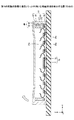
従来より、被接続物を実装基板等と電気的に接続するソケットが知られている。図1は、従来のソケットを例示する断面図(その1)である。図1を参照するに、従来のソケット100は、支持体101と、ばね性を有する導電性の接続端子102及び103とを有する。支持体101には複数の貫通孔101xが所定のピッチで配設されている。支持体101の一方の面101aには配線104が形成され、配線104は一方の面101aから貫通孔101xを介して他方の面101bに延在している。
Conventionally, a socket for electrically connecting an object to be connected to a mounting board or the like is known. FIG. 1 is a cross-sectional view (part 1) illustrating a conventional socket. Referring to FIG. 1, a
接続端子102の一端は、支持体101の一方の面101aに形成された配線104上に固定されている。接続端子102の他端は、被接続物400のパッド401と接触可能に構成されている。接続端子103の一端は、支持体101の他方の面101bに形成された配線104上に固定されている。接続端子103の他端は、マザーボード等の実装基板500と電気的に接続されている。なお、接続端子102と接続端子103とは同一部品としても構わない。
One end of the
パッド401を有する被接続物400(例えば、配線基板や半導体パッケージ等)がソケット100の方向に押圧されると、接続端子102の他端はパッド401と接触する。これにより、ソケット100と被接続物400とは電気的に接続される。すなわち、被接続物400は、ソケット100を介してマザーボード等の実装基板500と電気的に接続される(例えば、特許文献1参照)。
When an object to be connected 400 having a pad 401 (for example, a wiring board or a semiconductor package) is pressed toward the
図2は、従来のソケットを例示する断面図(その2)である。図2を参照するに、従来のソケット200は、ソケット100(図1参照)とは異なり、接続端子102に代えて接続端子202を有する。接続端子202はばね性を有する導電性の接続端子であり、その一端は支持体101の一方の面101aに形成された配線104上に固定されている。接続端子202の他端は、被接続物400のパッド401と接触可能に構成されている。又、従来のソケット200は、ソケット100(図1参照)とは異なり、接続端子103に代えてバンプ203を有する。支持体101の他方の面101bに形成された配線104は、バンプ203を介して、マザーボード等の実装基板500と電気的に接続されている。
FIG. 2 is a cross-sectional view (part 2) illustrating a conventional socket. Referring to FIG. 2, the
パッド401を有する被接続物400(例えば、配線基板や半導体パッケージ等)がソケット200の方向に押圧されると、接続端子202の他端はパッド401と接触する。これにより、ソケット200と被接続物400とは電気的に接続される。すなわち、被接続物400は、ソケット200を介してマザーボード等の実装基板500と電気的に接続される(例えば、特許文献2参照)。
When an object to be connected 400 having a pad 401 (for example, a wiring board or a semiconductor package) is pressed in the direction of the
図3は、従来のソケットを例示する断面図(その3)である。図3を参照するに、従来のソケット300は、樹脂を成形したハウジング301と、ばね性を有する導電性の接続端子302とを有する。
FIG. 3 is a cross-sectional view (part 3) illustrating a conventional socket. Referring to FIG. 3, a
ハウジング301には、複数の貫通孔301xが所定のピッチで配設されている。接続端子302は、一体的に構成された接続部315及び316とばね部317とを有し、ハウジング301の貫通孔301x内に固定(嵌合)されている。接続部315はハウジング301の一方の面301aから突出しており、接続部316はハウジング301の他方の面301bから露出している。
The housing 301 is provided with a plurality of through holes 301x at a predetermined pitch. The
接続部316は、バンプ303を介して、マザーボード等の実装基板500と電気的に接続されている。パッド401を有する被接続物400(例えば、配線基板や半導体パッケージ等)がソケット300の方向に押圧されると、接続部315はパッド401と接触する。これにより、ソケット300と被接続物400とは電気的に接続される。すなわち、被接続物400は、ソケット300を介してマザーボード等の実装基板500と電気的に接続される(例えば、特許文献3参照)。
The connection portion 316 is electrically connected to the
ところで、図1に示すソケット100では、支持体101の両面(一方の面101a及び他方の面101b)に接続端子102及び103が形成されており、接続端子102、配線104(貫通孔101x内に形成されたものも含む)、及び接続端子103が被接続物400と実装基板500との間の信号の伝送経路となる。そのため、ソケット100の高さが高くなると共に、被接続物400と実装基板500との接続距離(信号の伝送経路)が長くなる。つまり、このような構造は、ソケット100の低背化を阻害する要因となると共に、高速信号伝搬を阻害する要因ともなる。
By the way, in the
又、図2に示すソケット200では、支持体101の片面(一方の面101a)に接続端子202が形成されており、接続端子202、配線104(貫通孔101x内に形成されたものも含む)、及びバンプ203が被接続物400と実装基板500との間の信号の伝送経路となる。接続端子103がバンプ203に置き換わった分だけソケット100よりは低背化が可能であり、又、被接続物400と実装基板500との接続距離(信号の伝送経路)の短縮も可能である。しかしながら、接続端子202に支持体101の厚みが加わるため、十分な低背化を実現できるとは言い難い。又、被接続物400から実装基板500に至る信号は、支持体101の貫通孔101x内に形成された配線104を経由するため、被接続物400と実装基板500との接続距離(信号の伝送経路)を十分に短縮できるとは言い難い。
In the
更に、図3に示すソケット300では、ハウジング301の貫通孔301x内には配線が形成されてなく、貫通孔301x内に一部が固定された接続端子302とバンプ303のみが被接続物400と実装基板500とを接続している。従って、一見すると、十分な低背化が実現できると共に、被接続物400から実装基板500までの接続距離(信号の伝送経路)を十分に短縮できるとも思える。
Further, in the
しかしながら、接続端子302において貫通孔301x内に固定(嵌合)された部分は、ばねとして機能できず、ばねとして機能できるのは主にハウジング301の一方の面301aから突出している部分のみである。そのため、接続端子302がばねとして十分に機能するためには、一方の面301aからの突出部分をある程度延ばさざるを得ない。又、貫通孔301x内に接続端子302の一部を固定(嵌合)するためには、ハウジング301の厚さをある程度確保する必要がある。結果として、ソケット300の十分な低背化を実現できず、被接続物400から実装基板500までの接続距離(信号の伝送経路)も十分に短縮できない。
However, the portion fixed (fitted) in the through-hole 301x in the
本発明は、上記の点に鑑みてなされたものであり、低背化を実現できると共に、被接続物と実装基板等との接続距離を短縮可能なソケット及びその製造方法を提供することを課題とする。 The present invention has been made in view of the above points, and it is an object of the present invention to provide a socket capable of reducing the height and reducing the connection distance between an object to be connected and a mounting substrate, and a method for manufacturing the same. And
本ソケットは、一端に第1の接続部が形成され、他端に被接続物により押圧された際に前記被接続物のパッドと接触する第2の接続部が形成された接続端子を備え、前記接続端子を介して前記被接続物を着脱可能な状態で基板に接続するソケットであって、前記接続端子を固定する支持体と、前記支持体に形成された貫通孔と、を有し、前記接続端子は、金属板を湾曲して形成されてなり、前記第1の接続部と、前記第1の接続部に対して対向配置された前記第2の接続部と、湾曲した形状とされ、ばね性を有するばね部と、一方の端部が前記ばね部と一体的に構成され、他方の端部が前記第1の接続部の端部と一体的に構成された板状の第1の支持部と、一方の端部が前記ばね部と一体的に構成され、他方の端部が前記第2の接続部の端部と一体的に構成された板状の第2の支持部と、を有し、前記第1の支持部は前記基板の表面に対して鋭角になるように傾斜し、前記第2の接続部は、前記第2の支持部から前記被接続物のパッドに向かう方向に突出すると共に、前記第2の支持部と一体的に構成された突出部と、前記突出部の端部に設けられ、前記被接続物のパッドと接触する接触部と、を有し、前記被接続物のパッドと接触する部分の前記接触部はラウンド形状であり、前記接続端子は前記貫通孔に挿入され、前記第1の接続部が前記支持体の一方の面に固着され、前記第2の接続部が前記支持体の他方の面から突出していることを要件とする。 The socket includes a connection terminal in which a first connection portion is formed at one end, and a second connection portion is formed at the other end that comes into contact with a pad of the connection object when pressed by the connection object. A socket for connecting the object to be connected to the substrate via the connection terminal in a detachable state, and a support body for fixing the connection terminal, and a through hole formed in the support body, The connection terminal is formed by curving a metal plate, and has a curved shape with the first connection portion, the second connection portion disposed to face the first connection portion. The spring-like spring part, and one end part is configured integrally with the spring part, and the other end part is configured integrally with the end part of the first connection part. and the support portion, which one end is configured the spring portion integral with the end portion of the other end the second connecting portion And a second support portion of the integrally constructed plate, wherein the first support portion is inclined to become an acute angle with respect to the surface of the substrate, said second connecting portion, A protrusion projecting in a direction from the second support portion toward the pad of the connected object, a protrusion portion integrally formed with the second support portion, and an end portion of the protrusion portion; A contact portion that contacts the pad of the connection object, the contact portion of the portion that contacts the pad of the connection object has a round shape, the connection terminal is inserted into the through hole, and the first It is a requirement that the connecting portion is fixed to one surface of the support, and the second connecting portion protrudes from the other surface of the support.
本ソケットの製造方法は、一端に第1の接続部が形成され他端に第2の接続部が形成された接続端子を備え、前記接続端子を介して被接続物を着脱可能な状態で基板に接続するソケットの製造方法であって、前記接続端子を形成する第1工程と、前記接続端子を固定する支持体を準備し、前記支持体に貫通孔を形成する第2工程と、前記貫通孔に対応する位置に前記接続端子を収容する開口部が設けられた治具を準備し、前記貫通孔と前記開口部とが対応する位置にくるように、前記治具上に前記支持体を載置する第3工程と、前記接続端子を、前記第2の接続部が前記開口部に挿入されると共に、前記第1の接続部が前記支持体の一方の面に接するように配置する第4工程と、前記第1の接続部を前記支持体の一方の面に固着する第5工程と、前記治具を取り外す第6工程と、を有することを要件とする。 The method of manufacturing the socket includes a connection terminal having a first connection portion formed at one end and a second connection portion formed at the other end, and the substrate can be attached and detached via the connection terminal. A method of manufacturing a socket to be connected to a first step of forming the connection terminal, a second step of preparing a support for fixing the connection terminal, and forming a through hole in the support, and the penetration Prepare a jig provided with an opening for accommodating the connection terminal at a position corresponding to the hole, and place the support on the jig so that the through hole and the opening are at a corresponding position. And a third step of placing the connection terminal, wherein the second connection portion is inserted into the opening and the first connection portion is in contact with one surface of the support. 4 process and 5th process which adheres the said 1st connection part to one surface of the said support body It may be a requirement that has a, a sixth step of removing the jig.
開示の技術によれば、低背化を実現できると共に、被接続物と実装基板等との接続距離を短縮可能なソケット及びその製造方法を提供できる。 According to the disclosed technology, it is possible to provide a socket capable of realizing a low profile and capable of shortening a connection distance between an object to be connected and a mounting substrate, and a manufacturing method thereof.
以下、図面を参照して発明を実施するための形態について説明する。なお、各図面において、同一構成部分には同一符号を付し、重複した説明を省略する場合がある。 Hereinafter, embodiments for carrying out the invention will be described with reference to the drawings. In addition, in each drawing, the same code | symbol is attached | subjected to the same component and the overlapping description may be abbreviate | omitted.
なお、以下の実施の形態及びその変形例では、一例として、半導体パッケージ及び支持体の平面形状が矩形状である場合を示すが、半導体パッケージ及び支持体の平面形状は矩形状には限定されず、任意の形状として構わない。 Note that, in the following embodiments and modifications thereof, as an example, the planar shape of the semiconductor package and the support is rectangular, but the planar shape of the semiconductor package and the support is not limited to a rectangular shape. Any shape can be used.
〈第1の実施の形態〉
[第1の実施の形態に係るソケットの構造]
図4は、第1の実施の形態に係るソケットを例示する断面図である。図5は、図4の一部を拡大して例示する断面図である。図4及び図5を参照するに、ソケット10は、支持体20と、接続端子30と、位置決め部40と、バンプ50とを有する。但し、後述のように、位置決め部40及びバンプ50は、ソケット10の必須の構成要素ではなく、支持体20及び接続端子30のみがソケット10の必須の構成要素である。
<First Embodiment>
[Structure of socket according to the first embodiment]
FIG. 4 is a cross-sectional view illustrating the socket according to the first embodiment. FIG. 5 is an enlarged cross-sectional view illustrating a part of FIG. Referring to FIGS. 4 and 5, the
60は被接続物である半導体パッケージを、70はマザーボード等の実装基板を、80は筐体を示している。半導体パッケージ60は、ソケット10を介して、実装基板70と電気的に接続されている。なお、第1の実施の形態では、被接続物として半導体パッケージ60を例示して説明するが、被接続物は半導体チップを有さない配線基板等であっても構わない。
支持体20は、貫通孔21xが設けられた本体21と、本体21の一方の面21aに設けられた接着層22とを有する。本体21は、接続端子30を固定するための基体となるものであり、例えば、ポリイミド樹脂や液晶ポリマ等を用いたフレキシブルなフィルム状基板を用いることができる。本体21として、ガラスクロスにエポキシ系樹脂等の絶縁性樹脂を含浸したリジッドな基板(例えば、FR4材)等を用いても構わない。本体21の厚さは、例えば50〜400μm程度とすることができるが、100μm程度にすると好適である。
The
貫通孔21xは、接続端子30を挿入するための孔であり、被接続物である後述する半導体パッケージ60の貴金属層65(パッド)に対応する個数設けられている。貫通孔21xの平面形状は、接続端子30の平面形状に合わせて適宜決定できるが、例えば平面形状が矩形状等の孔とすることができる。なお、貫通孔21x内も含めた本体21には、配線パターンやビア配線等の導体は設けられていない。
The through
接着層22は、接続端子30を本体21に固定するための層であり、本体21の一方の面21aに設けられている。接着層22としては、エポキシ系やシリコーン系等の熱硬化性の接着剤、或いは液晶ポリマ材等の熱可塑性の接着剤等を用いることができる。
The
接着層22は、ソケット10の製造工程においてはんだリフロー等により加熱された場合や、半導体パッケージ60の発熱やソケット10の使用される環境温度等により高温になった場合等に溶融しない材料を選定することが好ましい。なお、接着層22は、本体21の一方の面21aの全面に設けても良いが、本体21の一方の面21aの接続端子30を固定する部分近傍のみに設けても良い。
The
接続端子30は、ばね性を有する導電性の部材である。接続端子30は、本体21に設けられた貫通孔21xに挿入され、その一端(後述する第1の接続部31の一方の面31a側)は、接着層22を介して本体21の一方の面21aに固着されている。又、接続端子30の他端(後述する第2の接続部32)は、本体21の他方の面21bから突出している。なお、接続端子30は、ばねとして機能できる状態で貫通孔21xに挿入されている。つまり、接続端子30の貫通孔21xに挿入された部分は、貫通孔21xの内壁面には固定されてなく弾性変形可能である。そのため、接続端子30は、貫通孔21xに挿入された部分も含めてほぼ全体(後述する第1の接続部31を除く部分)がばねとして機能できる。
The
接続端子30の一端(後述する第1の接続部31の他方の面31b側)は、バンプ50を介して、後述する実装基板70の導体層72(パッド)と接合され、導体層72と電気的に接続されている。つまり、接続端子30において、後述する第1の接続部31の他方の面31bは、外部(実装基板70等)との接続部である。接続端子30の他端(後述する第2の接続部32)は、後述する半導体パッケージ60の貴金属層65に離間可能な状態(固定されていない状態)で接触し、貴金属層65と電気的に接続されている。接続端子30の詳細な構造については、後述する。
One end of the connection terminal 30 (the
なお、領域A(図4参照)に配置された接続端子30と、領域B(図4参照)に配置された接続端子30とは、対向するように(対称に)配置されている。このような配置により、接続端子30がZ方向に押圧されたときに、横方向(Z方向以外の方向)に生じる反力を低減できる。特に、接続端子30の数が多いときに有効である。但し、例えば接続端子30の数が比較的少ない場合のように、横方向(Z方向以外の方向)に生じる反力が問題にならない場合には、領域Aの接続端子30と領域Bの接続端子30とが同一方向を向くように配置しても構わない。
In addition, the
位置決め部40は、例えばエポキシ系樹脂等を主成分とする平面形状が額縁状の部材である。位置決め部40の底面は、支持体20を構成する本体21の他方の面21bの外縁部に接着剤等により固着されている。位置決め部40は、ねじ等を用いて支持体20と機械的に固着しても構わない。位置決め部40の内側面の形成する空間の平面形状は、後述の半導体パッケージ60の基板61の平面形状と略同一であり、半導体パッケージ60を挿入可能に構成されている。
The positioning
位置決め部40の内側面は、挿入された半導体パッケージ60の基板61の側面と接し、半導体パッケージ60とソケット10とを位置決めする。これにより、半導体パッケージ60の各貴金属層65と、ソケット10を構成する各接続端子30の後述する第2の接続部32とが接触する。位置決め部40は、半導体パッケージ60とソケット10とを位置決めする機能に加えて、支持体20の強度を補強する機能も有する。
The inner side surface of the
なお、位置決め部40はソケット10の必須の構成要素ではなく、例えば位置決め部40を設けずに、後述の筐体80の枠部81により半導体パッケージ60を位置決めする構造にしても構わない。
The
バンプ50は、接続端子30の一端(後述する第1の接続部31の他方の面31b側)に形成されている。バンプ50は、接続端子30の一端(後述する第1の接続部31)を、後述する実装基板70の導体層72と電気的に接続している。バンプ50としては、例えば、はんだを用いることができる。はんだの材料としては、例えば、Pbを含む合金、SnとCuの合金、SnとAgの合金、SnとAgとCuの合金等の鉛フリーはんだを用いることが好ましい。バンプ50として、はんだの代わりに、例えば導電性樹脂接着剤(例えば、Agペースト)等を用いても構わない。なお、バンプ50はソケット10の必須の構成要素ではなく、例えばソケット10にバンプ50を設けずに、後述の実装基板70の導体層72上にはんだや導電性樹脂接着剤等からなるバンプを設けても構わない。
The
被接続物である半導体パッケージ60は、基板61と、半導体チップ62と、封止樹脂63と、導体層64と、貴金属層65とを有する。基板61は、例えば絶縁性樹脂を含む基板本体に絶縁層、配線パターン、ビア配線等(図示せず)が形成されたものである。基板61の一方の面にはシリコン等を含む半導体チップ62が実装され、他方の面には例えば銅(Cu)からなる配線パターンの一部である導体層64が形成されている。
A
導体層64の材料は、例えば、銅(Cu)等である。導体層64の厚さは、例えば、5〜10μm程度である。半導体チップ62は、例えばフリップチップ接続により基板61に搭載され、絶縁性樹脂からなる封止樹脂63により封止されている。なお、半導体チップ62の背面を露出するように封止樹脂63を設け、半導体チップ62の背面に例えば銅(Cu)等からなる放熱板を配置しても構わない。
The material of the
貴金属層65は、導体層64の上面に積層形成されている。導体層64及び貴金属層65は、基板61の他方の面に、例えば格子状に配置されたパッドである。すなわち、半導体パッケージ60は所謂LGA(Land grid array)であり、ソケット10は所謂LGA用のソケットである。
The
貴金属層65としては、例えば、金(Au)層やパラジウム(Pd)層等の貴金属を含む層を用いることができる。貴金属層65は、例えば、無電解めっき法等により形成できる。なお、金(Au)層の下層として、ニッケル(Ni)層やNi/Pd層(Ni層とPd層をこの順番で積層した金属層)等を形成しても構わない。
As the
貴金属層65は、接続端子30との接続信頼性を向上するために設けられている。貴金属層65は、接続端子30との接触抵抗を安定させるため、通常の金めっき層等に比べて大幅に厚く形成されている。はんだボール等との接続信頼性を向上するために通常設けられる金めっき層等の厚さは、0.05μm以下程度である。これに対して、貴金属層65の厚さは、例えば、0.4μm程度であり、通常設けられる金めっき層等の8倍以上の厚さとされている。
The
実装基板70(マザーボード等)は、基板本体71と、導体層72(パッド)とを有する。導体層72は、基板本体71の一方の面に形成されている。基板本体71は、例えば、ガラスクロスにエポキシ樹脂等の絶縁性樹脂を含浸したもの等である。導体層72の材料は、例えば、銅(Cu)等である。
The mounting substrate 70 (motherboard or the like) has a
筐体80は、枠部81と、蓋部82とを有する。枠部81は、位置決め部40の外側面の更に外側に設けられた平面形状が額縁状の部材である。枠部81の材料としては、剛性のある金属や樹脂等を用いることが好ましい。枠部81は、実装基板70を貫通するボルト等(図示せず)により、実装基板70の上面に固着されている。
The
蓋部82は、例えば金属や樹脂等で構成される平面形状が略矩形状や略額縁状の部材である。蓋部82は、例えば枠部81の上面の一端側に回動可能に取り付けられており、他端側にロック機構を有する。蓋部82の外縁部を枠部81の上面と接するように固定する(ロックする)ことにより(図4及び図5の状態)、蓋部82が半導体パッケージ60を実装基板70側に押し込み、半導体パッケージ60は実装基板70側に移動する。
The
これにより、ソケット10の接続端子30は押圧されZ方向に縮んで所定のばね圧が生じ、半導体パッケージ60の貴金属層65は接続端子30の他端(後述する第2の接続部32)と接触する。つまり、半導体パッケージ60はソケット10を介して実装基板70と電気的に接続される。但し、蓋部82のロックを解除することにより、半導体パッケージ60は、ソケット10から着脱可能である。
As a result, the
なお、蓋部82は、枠部81とは別体でも構わない。この場合には、例えば、半導体パッケージ60を蓋部82により上側から押圧した状態で、蓋部82が枠部81に固定可能な構造であれば良い。
The
このように、ソケット10は、従来のソケット100(図1参照)のように、接続端子102及び103が支持体101の両面から突出する構造ではなく、支持体20の片面から接続端子30が突出する構造である。そのため、接続端子30の一端から他端までの距離を短くできる。その結果、ソケット10を従来のソケット100より低背化できると共に、被接続物である半導体パッケージ60とマザーボード等の実装基板70との接続距離(信号の伝送経路)を短縮できる。 又、ソケット10は、従来のソケット200(図2参照)のように、被接続物から実装基板に至る信号が、接続端子202及び支持体101の貫通孔101x内に形成された配線104を経由する構造ではなく、配線が設けられていない貫通孔21x内に挿入された接続端子30の一端に設けられたバンプ50を介して直接実装基板70に接続された構造である。その結果、支持体20の厚さが低背化を阻害する要因ではなくなるため、ソケット10を従来のソケット200より低背化できると共に、被接続物である半導体パッケージ60とマザーボード等の実装基板70との接続距離(信号の伝送経路)を短縮できる。
As described above, the
又、ソケット10は、従来のソケット300(図3参照)のように、貫通孔301x内に接続端子302の一部が固定(嵌合)された構造ではなく、接続端子30がばねとして機能できる状態で貫通孔21xに挿入された構造である。つまり、接続端子30の貫通孔21xに挿入された部分は、貫通孔21xの内壁面には固定されてなく弾性変形可能である。そのため、接続端子30は、貫通孔21xに挿入された部分も含めてほぼ全体(後述する第1の接続部31を除く部分)がばねとして機能でき、接続端子30自体を従来のソケット300の接続端子302より低背化することが可能となる。
The
その結果、ソケット10を従来のソケット300より低背化できると共に、被接続物である半導体パッケージ60とマザーボード等の実装基板70との接続距離(信号の伝送経路)を短縮できる。なお、接続距離(信号の伝送経路)を短縮することにより、寄生インダクタ、寄生容量、寄生抵抗等を低減できるため、高速信号伝送に対応可能となる。又、ソケット10では、貫通孔21x内に配線が設けられていないため、余計な絶縁層を設ける必要がない。この点も寄生容量の低減に寄与し、高速信号伝送に有利となる。
As a result, the height of the
又、ソケット10は、支持体20に、ばね性を有する接続端子30を直接固定し、従来のソケット300(図3参照)のような反りの原因となるハウジングが存在しない構造としているため、反りの発生し難いソケットを実現できる。反りの発生を抑制することにより、半導体パッケージ60と実装基板70との接続信頼性を向上可能となる。
Further, the
ここで、図6を参照しながら、接続端子30の詳細な構造について説明する。接続端子30は、ばね性を有する導電性の部材であり、第1の接続部31と、第2の接続部32と、ばね部33と、第1の支持部34と、第2の支持部35とを有する。
Here, the detailed structure of the
第1の接続部31は、接続端子30の一端に形成されている。第1の接続部31は、板状とされている。第1の接続部31の厚さ(Z方向)は、例えば0.08mm程度とすることができる。第1の接続部31の横幅(Y方向)は、例えば0.4mm程度とすることができる。第1の接続部31の縦幅(X方向)は、例えば0.4mm程度とすることができる。
The
第1の接続部31の一方の面31aは、例えば、接着層22を介して本体21の一方の面21aに固着される面である。第1の接続部31の他方の面31bは、外部(実装基板70等)との接続部となる面である。第1の接続部31の他方の面31bは、一例として、他方の面31bに設けられたバンプ50を介して実装基板70と接合され電気的に接続される。第1の接続部31の他方の面31bは、他の例として、実装基板70側に設けられたバンプと離間可能な状態(固定されていない状態)で接触し電気的に接続される。
One
第2の接続部32は、接続端子30の他端に形成され、第1の接続部31と対向するように配置されている。第2の接続部32は、ばね部33、第1の支持部34、及び第2の支持部35を介して、第1の接続部31と電気的に接続されている。第2の接続部32は、接触部38と、突出部39とを有する。第2の接続部32の厚さは、例えば0.08mm程度とすることができる。第2の接続部52の横幅(Y方向)は、例えば、0.2mm程度とすることができる。
The
接触部38は、被接続物のパッド(例えば半導体パッケージ60の貴金属層65等)と接触する部分である。接触部38はラウンド形状とされており、接続端子30が押圧された際、主にZ方向に移動する。このように、接触部38をラウンド形状とすることにより、接触部38が押圧され貴金属層65等と接触する際、接触部38により貴金属層65等が破損することを防止できる。
The
又、接触部38は、例えば半導体パッケージ60が第2の接続部32を押圧した際、ばね部33の変形により、第2の接続部32が第1の接続部31に近づく方向(Z方向)に移動した状態で、貴金属層65等と接触する。これにより、貴金属層65等と第2の接続部32とが接触した際、第2の接続部32が、貴金属層65等が形成された面と平行な方向に大きく移動することがなくなるため、貴金属層65等を狭ピッチに配置できる。貴金属層65等のピッチ(接触部38のピッチ)としては、例えば、0.4〜1.5mm程度とすることができる。
Further, the
突出部39は、一方の端部が第2の支持部35と一体的に構成されており、他方の端部が接触部38と一体的に構成されている。突出部39は、第2の支持部35から貴金属層65等に向かう方向(第1の接続部31から離間する方向)に突出している。
One end of the protruding
このように、接触部38と第2の支持部35との間に、接触部38及び第2の支持部35と一体的に構成され、第2の支持部35から貴金属層65等に向かう方向(第1の接続部31から離間する方向)に突出する突出部39を設けることにより、以下の効果を奏する。すなわち、半導体パッケージ60等が接触部38を押圧した際の、ばね部33の変形による貴金属層65等と第2の支持部35との接触を防止することが可能となり、接続端子30及び貴金属層65等の破損を防止できる。
In this way, the
貴金属層65等と第2の接続部32とが接触していない状態における第2の接続部32の突出量C(第2の支持部35と突出部39との接続部分を基準としたときの突出量)は、例えば、0.3mmとすることができる。
Projection amount C of the
ばね部33は、第1の支持部34と第2の支持部35との間に配置されており、第1の支持部34及び第2の支持部35と一体的に構成されている。ばね部33は、湾曲した形状(例えば、C字型)とされており、ばね性を有する。
The
ばね部33は、半導体パッケージ60等により第2の接続部32が押圧された際、第2の接続部32を貴金属層65等に向かう方向に反発させることで、第2の接続部32と貴金属層65等とを固定することなく接触させるためのものである。ばね部33の横幅(Y方向)及び厚さは、例えば、第2の接続部32の横幅(Y方向)及び厚さと同じにすることができる。
When the
なお、本実施の形態の接続端子30では、実際には、第1の支持部34、ばね部33、第2の支持部35、及び第2の接続部32が一体的にばねとして機能する。第1の支持部34、ばね部33、第2の支持部35、及び第2の接続部32に対応する部分の接続端子30のばね定数は、例えば、0.6〜0.8N/mmとすることができる。
In the
第1の支持部34は、ばね部33と第1の接続部31との間に配置されている。第1の支持部34の一方の端部は、ばね部33の一方の端部と一体的に構成されており、第1の支持部34の他方の端部は、第1の接続部31と一体的に構成されている。第1の支持部34は、板状とされている。
The
第1の支持部34は、実装基板70等と対向する側の第1の接続部31の面31bを含む平面Dと、実装基板70等と対向する側の第1の支持部34の面34aとが成す角度θ1が鋭角となるように構成されている。角度θ1は、例えば、5〜15度とすることができる。
The
このように、角度θ1を鋭角にすることで、半導体パッケージ60等が接触部38を押圧した際のばね部33の変形による実装基板70等と第1の支持部34との接触を防止することが可能となるため、接続端子30及び実装基板70等の破損を防止できる。第1の支持部34の横幅(Y方向)及び厚さは、例えば、第2の接続部32の横幅(Y方向)及び厚さと同じにすることができる。
Thus, by making the angle θ 1 an acute angle, the contact between the mounting
第2の支持部35は、ばね部33と第2の接続部32との間に配置されている。第2の支持部35の一方の端部は、ばね部33の一方の端部と一体的に構成されており、第2の支持部35の他方の端部は、第2の接続部32の突出部39と一体的に構成されている。第2の支持部35は、板状とされている。第2の支持部35の横幅(Y方向)及び厚さは、例えば、第2の接続部32の横幅(Y方向)及び厚さと同じにすることができる。
The
図6に示す状態(接続端子30の第2の接続部32が押圧されていない状態)における接続端子30の高さHは、例えば、1〜2mm程度とすることができるが、1.6mm程度とすると好適である。
The height H of the
[第1の実施の形態に係るソケットの製造方法]
次に、図7〜図14を参照しながら、ソケット10の製造方法について説明する。なお、図7及び図9〜図11において、支持体20等は図4及び図5とは上下が反転した状態で描かれている。
[Method of Manufacturing Socket According to First Embodiment]
Next, a method for manufacturing the
始めに、図7(断面図)及び図8(平面図)に示す工程では、本体21の一方の面21aに接着層22が設けられた支持体20を準備し、本体21に貫通孔21xを形成する。貫通孔21xは、例えば本体21を接着層22ごとプレス加工(打ち抜き加工)により型抜きすることで形成できる。貫通孔21xは、半導体パッケージ60の貴金属層65(パッド)に対応する個数形成する。貫通孔21xは、例えば平面形状が矩形状の孔とすることができる。
First, in the process shown in FIG. 7 (sectional view) and FIG. 8 (plan view), a
ここでは一例として、支持体20の本体21としてポリイミドフィルムを用い、接着層22としてシリコーン系の熱硬化性接着剤を用いる。本体21や接着層22として、第1の実施の形態に係るソケット10の構造の説明に記載した他の材料を用いても構わない。接着層22は、後述の図11に示す工程においてリフロー等により加熱された場合や、半導体パッケージ60の発熱やソケット10の使用される環境温度等により高温になった場合等に溶融しない材料を選定することが好ましい。なお、図7では支持体20の本体21の一方の面21aの全面に接着層22を設けているが、本体21の一方の面21aの接続端子30を固定する部分近傍のみに接着層22を設けても良い。
Here, as an example, a polyimide film is used as the
次いで、図9に示す工程では、支持体20を治具25上に載置する。治具25は、接続端子30の高さH(図6参照)よりも厚く作製されており、支持体20の貫通孔21xに対応する位置に貫通孔25xを有する。支持体20は、本体21の他方の面21bが治具25の上面と接すると共に、貫通孔21xと貫通孔25xとが平面視において重なるように治具25上に載置する。なお、治具25において、貫通孔25xに代えて、接続端子30の高さH以上の深さを有する凹部を設けても構わない。
Next, in the step shown in FIG. 9, the
次いで、図10に示す工程では、接続端子30を作製する。そして、作製した接続端子30を第2の接続部32側から貫通孔21x及び25xに挿入し、第1の接続部31の一方の面31aが接着層22に接するように仮固定する。更に、各接続端子30を接着層22側に加圧した状態で、接着層22を硬化温度以上に加熱し、第1の接続部31を接着層22を介して支持体20の本体21に固着する。
Next, in the process illustrated in FIG. 10, the
接続端子30は、例えば、図示していない金属板(例えば、Cu系合金)を所定の形状に打ち抜き加工した後、打ち抜かれた金属板の表面全体にNiめっき膜(例えば、厚さ1〜3μm)を形成し、次いで、第1の接続部31及び接触部38に対応する部分に形成されたNiめっき膜に、Auめっき膜(例えば、厚さ0.3〜0.5μm)を積層形成(Auめっき膜を部分的に形成)し、その後、Niめっき膜及びAuめっき膜が形成され、打ち抜かれた金属板を曲げ加工することで作製できる。
The
上記金属板の材料となるCu系合金としては、例えば、リン青銅やベリリウム銅、コルソン系の銅合金等を用いることができる。なお、接続端子30は、図示していない金属板(例えば、Cu系合金)を所定の形状にエッチング加工した後、エッチング加工された金属板を曲げ加工することで形成してもよい。
For example, phosphor bronze, beryllium copper, Corson copper alloy, or the like can be used as the Cu alloy used as the material of the metal plate. The
次いで、図11に示す工程では、第1の接続部31の他方の面31bに、はんだを載置(はんだペーストの塗布やはんだボールの搭載等)してリフローし、バンプ50を形成する。はんだの材料としては、例えば、Pbを含む合金、SnとCuの合金、SnとAgの合金、SnとAgとCuの合金等の鉛フリーはんだを用いることができる。はんだの代わりに、例えば、導電性樹脂接着剤(例えば、Agペースト)等を用いても構わない。
Next, in the step shown in FIG. 11, solder is placed on the
なお、前述のように、接続端子30の表面にはNiめっき膜が形成され、第1の接続部31にはNiめっき膜上に更にAuめっき膜が積層形成されている。そのため、はんだは第1の接続部31のみに形成され易くなり、Auめっき膜が積層形成されていない部分(Niめっき膜が露出する部分)に、はんだが濡れ上がる虞を低減できる。
As described above, the Ni plating film is formed on the surface of the
なお、例えばソケット10にバンプ50を設けずに、実装基板70の導体層72上にはんだや導電性樹脂接着剤等からなるバンプを設けても構わない。その場合には、この工程は不要となる。
For example, without providing the
次いで、図12に示す工程では、支持体20から治具25を取り外し上下を反転させる。次いで、図13(断面図)及び図14(平面図)に示す工程では、支持体20を構成する本体21の他方の面21bの外縁部に接着剤等により位置決め部40を固着する。位置決め部40は、ねじ等を用いて支持体20と機械的に固着しても構わない。位置決め部40としては、例えばエポキシ系樹脂等を主成分とする平面形状が額縁状の部材を用いることができる。なお、筐体80により半導体パッケージ60を位置決め保持する構造等の場合には、位置決め部40は設けなくても構わない。その場合には、この工程は不要となる。以上の図7〜図14に示す工程により、ソケット10が完成する。
Next, in the step shown in FIG. 12, the
[第1の実施の形態に係るソケットの使用方法]
次に、図15〜図17を参照しながら、ソケット10を用いた半導体パッケージ60と実装基板70との接続方法について説明する。
[Method of using socket according to first embodiment]
Next, a method for connecting the
始めに、図15に示すように、実装基板70及びソケット10を準備する。そして、実装基板70とソケット10とを、バンプ50を介して接合し電気的に接続する。具体的には、実装基板70の導体層72とソケット10のバンプ50とを接触させる。そして、バンプ50を例えば230℃に加熱して溶融させ、その後硬化させて、実装基板70とソケット10とを接合する。これにより、ソケット10は、バンプ50を介して実装基板70と電気的に接続される。
First, as shown in FIG. 15, a mounting
次いで、図16に示すように、筐体80を準備し、筐体80を構成する枠部81を実装基板70を貫通するボルト等(図示せず)により、実装基板70の上面に固着する。そして、筐体80を構成する蓋部82を矢印方向に回動させて、半導体パッケージ60を配置可能な状態とする。
Next, as shown in FIG. 16, a
次いで、図17に示すように、半導体パッケージ60を準備する。そして、半導体パッケージ60を位置決め部40に挿入し、基板61の側面が位置決め部40の内側面に接するように配置する。但し、この時点では、接続端子30は押圧されていない。半導体パッケージ60は、位置決め部40によりソケット10と位置合わせされ、半導体パッケージ60の各貴金属層65は各接続端子30の第2の接続部32と接触する。
Next, as shown in FIG. 17, a
更に、蓋部82を矢印方向に回動させて、半導体パッケージ60を実装基板70側に押し込み、蓋部82の外縁部が枠部81の上面と接するように固定(ロック)する。これにより、接続端子30は押圧されZ方向に縮んで所定のばね圧が生じ、半導体パッケージ60の各貴金属層65は各接続端子30の第2の接続部32と電気的に接続される。つまり、半導体パッケージ60はソケット10を介して実装基板70と電気的に接続される(図4及び図5の状態)。
Further, the
このように、第1の実施の形態に係るソケットは、ばね性を有する接続端子と貫通孔が設けられた支持体とを有し、接続端子はばねとして機能できる状態(貫通孔の内壁面に固定されていない状態)で支持体の貫通孔に挿入されている。そして、接続端子の一端は支持体の一方の面に固着され、接続端子の他端は支持体の他方の面から突出している。 Thus, the socket according to the first embodiment has a connection terminal having spring properties and a support body provided with a through hole, and the connection terminal can function as a spring (on the inner wall surface of the through hole). It is inserted into the through hole of the support body in a non-fixed state. One end of the connection terminal is fixed to one surface of the support, and the other end of the connection terminal protrudes from the other surface of the support.
つまり、支持体の厚さは、接続端子の高さの範囲内に収まっているため、支持体の厚さがソケットの低背化を阻害する要因ではなくなる。又、接続端子は、貫通孔に挿入された部分も含めてほぼ全体がばねとして機能できるので、貫通孔に固定するための部位を設けていた従来の接続端子よりも、接続端子自体を低背化できる。これらにより、従来よりもソケットを低背化することが可能となる。 That is, since the thickness of the support body is within the range of the height of the connection terminal, the thickness of the support body is no longer a factor that hinders the height reduction of the socket. In addition, since the entire connection terminal including the portion inserted into the through hole can function as a spring, the connection terminal itself has a lower height than the conventional connection terminal provided with a portion for fixing to the through hole. Can be As a result, the socket can be made shorter than before.
又、支持体の貫通孔に配線は設けられてなく、被接続物である半導体パッケージとマザーボード等の実装基板とは、接続端子と接続端子の一端に形成されたバンプのみを介して接続される。そのため、被接続物である半導体パッケージとマザーボード等の実装基板との接続距離(信号の伝送経路)を短縮できる。接続距離(信号の伝送経路)を短縮することで、寄生インダクタ、寄生容量、寄生抵抗等を低減でき、高速信号伝送に対応可能となる。 In addition, no wiring is provided in the through hole of the support, and the semiconductor package as a connected object and a mounting substrate such as a mother board are connected only via the bumps formed at one end of the connection terminal and the connection terminal. . Therefore, the connection distance (signal transmission path) between the semiconductor package as the connected object and a mounting substrate such as a mother board can be shortened. By shortening the connection distance (signal transmission path), parasitic inductors, parasitic capacitance, parasitic resistance, and the like can be reduced, and high-speed signal transmission can be supported.
又、貫通孔内に配線が設けられていないため、余計な絶縁層を設ける必要がない。この点も寄生容量の低減に寄与し、高速信号伝送に有利となる。 Further, since no wiring is provided in the through hole, it is not necessary to provide an extra insulating layer. This also contributes to the reduction of parasitic capacitance, which is advantageous for high-speed signal transmission.
又、支持体に、ばね性を有する接続端子を直接固定し、反りの原因となるハウジングが存在しない構造としているため、反りの発生し難いソケットを実現できる。反りの発生を抑制することにより、被接続物である半導体パッケージとマザーボード等の実装基板との接続信頼性を向上可能となる。 In addition, since the connection terminal having the spring property is directly fixed to the support body and the housing that causes the warp does not exist, a socket that does not easily warp can be realized. By suppressing the occurrence of warpage, it is possible to improve the connection reliability between a semiconductor package as a connected object and a mounting substrate such as a mother board.
〈第1の実施の形態の変形例1〉
第1の実施の形態では、複数の接続端子30を、接続端子30の配設方向に対して平行となるように配列する例を示した(図14参照)。第1の実施の形態の変形例1では、複数の接続端子30を、接続端子30の配設方向に対して傾斜するように配列する例を示す。以下、第1の実施の形態と共通する部分の説明は極力省略し、第1の実施の形態と相違する部分を中心に説明する。
<Variation 1 of the first embodiment>
In the first embodiment, an example in which a plurality of
図18は、第1の実施の形態の変形例1に係る接続端子の配列を例示する図である。図18を参照するに、複数の接続端子30は、接続端子30の配設方向Eに対して所定の角度θ2をなすように配列されている。言い換えれば、複数の接続端子30は、接続端子30の配設方向Eに対して傾斜するように配列されている。所定の角度θ2は、例えば、25〜35度程度とすることができる。
FIG. 18 is a diagram illustrating an arrangement of connection terminals according to the first modification of the first embodiment. Referring to FIG. 18, the plurality of
このように、複数の接続端子30を、接続端子30の配設方向Eに対して傾斜するように配列することにより、配設方向Eに対して平行となるように配列した場合と比較して、単位面積当たりに多くの接続端子30を配置することが可能となる。これにより、例えば0.4mm程度の狭ピッチでパッド(例えば、貴金属層65等)が配列された被接続物(半導体パッケージ60等)にも対応可能となる。
In this way, by arranging the plurality of
このように、第1の実施の形態の変形例1によれば、第1の実施の形態と同様の効果を奏するが、更に、以下の効果を奏する。すなわち、複数の接続端子を、接続端子の配設方向に対して傾斜するように配列することにより、配設方向に対して平行となるように配列した場合と比較して、より狭ピッチのLGA(Land grid array)に対応可能となる。 As described above, according to the first modification of the first embodiment, the same effects as those of the first embodiment are obtained, but the following effects are further obtained. That is, by arranging a plurality of connection terminals so as to be inclined with respect to the arrangement direction of the connection terminals, an LGA having a narrower pitch than that arranged in parallel to the arrangement direction. (Land grid array) can be supported.
〈第1の実施の形態の変形例2〉
第1の実施の形態では、バンプ50を設け、バンプ50を介して接続端子30の一端(第1の接続部31の他方の面31b側)を実装基板70の導体層72と接合し電気的に接続する例を示した。第1の実施の形態の変形例2では、実装基板70の導体層72と接触及び離間可能に構成されているバンプ50Aを設け、バンプ50Aを介して接続端子30の一端(第1の接続部31の他方の面31b側)を実装基板70の導体層72と離間可能な状態(固定されていない状態)で接触させることにより電気的に接続する例を示す。
<
In the first embodiment, bumps 50 are provided, and one end of the connection terminal 30 (the
図19は、第1の実施の形態の変形例2に係るソケットを例示する断面図である。図20は、図19の一部を拡大して例示する断面図である。図21A及び図21Bは、第1の実施の形態の変形例2に係る接続端子を例示する図である。図21Aが断面図、図21Bが斜視図である。図19〜図21Bを参照するに、ソケット10Aにおいて、バンプ50がバンプ50Aに置換されている点が、第1の実施の形態のソケット10(図4及び図5参照)と相違する。以下、第1の実施の形態と共通する部分の説明は極力省略し、第1の実施の形態と相違する部分を中心に説明する。
FIG. 19 is a cross-sectional view illustrating a socket according to
バンプ50Aは、第1の接続部31の他方の面31bに形成された突起部である。バンプ50Aは、実装基板70の導体層72と接触して導通しているが、導体層72に固定はされていない。つまり、バンプ50Aは、実装基板70の導体層72と離間可能な状態(固定されていない状態)で接触している。すなわち、蓋部82のロックを解除することにより、半導体パッケージ60のみならず、ソケット10Aも着脱可能である。そのため、接続端子30が破損したような場合であっても、容易にソケット10Aを良品と交換できる。
The
バンプ50Aは、第1の接続部31の他方の面31bに一体的に形成されたものでも、別体が接合されたものでも良い。バンプ50Aは、例えば他方の面31b側の面の径が先端部の径よりも大きい円錐台形状とすることができる。なお、円錐台とは、円錐を底面に平行な平面で切り、頂点を含む部分を除去した立体である。但し、バンプ50Aは、円錐台形状には限定されず、例えば半球状や円柱状、楕円柱状等としても構わない。バンプ50Aの他方の面31bからの突起量は、例えば0.3〜0.4mm程度とすることができる。
The
バンプ50Aは、前述の第1の実施の形態に係る接続端子30を作製する工程で、金属板(例えば、Cu系合金)を所定の形状に打ち抜き加工する際に同時にプレスにより形成することができる。又、バンプ50Aは、前述の第1の実施の形態に係る接続端子30を作製する工程で、金属板(例えば、Cu系合金)を所定の形状に打ち抜き加工した後、第1の接続部31の他方の面31bにめっき法やワイヤボンディングを用いて形成してもよい。この場合には、バンプ50Aの材料としては、金(Au)、銀(Ag)、銅(Cu)等を用いることができる。
The
このように、第1の実施の形態の変形例2によれば、第1の実施の形態と同様の効果を奏するが、更に、以下の効果を奏する。すなわち、第1の接続部の他方の面に実装基板のパッドと接触及び離間可能に構成されているバンプを形成し、形成したバンプを実装基板の導体層と離間可能な状態(固定されていない状態)で接触させ電気的に接続する。その結果、ソケットは実装基板から着脱可能となるため、接続端子が破損したような場合であっても、容易に良品と交換できる。 As described above, according to the second modification of the first embodiment, the same effects as those of the first embodiment are obtained, but the following effects are further obtained. That is, a bump configured to be able to contact and be separated from the pad of the mounting substrate is formed on the other surface of the first connecting portion, and the formed bump can be separated from the conductor layer of the mounting substrate (not fixed) Contact) and make electrical connection. As a result, since the socket can be detached from the mounting board, even if the connection terminal is damaged, it can be easily replaced with a non-defective product.
なお、バンプ50Aは、実装基板70側に設けても良い。バンプ50Aを実装基板70の導体層72上に設け、導体層72上に設けたバンプ50Aを第1の接続部31の他方の面31bと離間可能な状態(固定されていない状態)で接触させ電気的に接続することにより、同様の効果が得られる。バンプ50Aは、例えば、めっきやワイヤボンディング等により形成することができる。
The
〈第1の実施の形態の変形例3〉
第1の実施の形態では、バンプ50を、接続端子30の第1の接続部31の他方の面31bに形成する例を示した(図4及び図5参照)。第1の実施の形態の変形例3では、接続端子30の第1の接続部31の他方の面31bに突起部51を設け、突起部51を含む第1の接続部31の他方の面31bに接合部52を形成し、バンプ50Bとする例を示す。
<Modification 3 of the first embodiment>
In the first embodiment, an example in which the
図22は、第1の実施の形態の変形例3に係るソケットを例示する断面図である。図23は、図22の一部を拡大して例示する断面図である。図22及び図23を参照するに、ソケット10Bにおいて、バンプ50がバンプ50Bに置換されている点が、第1の実施の形態のソケット10(図4及び図5参照)と相違する。以下、第1の実施の形態と共通する部分の説明は極力省略し、第1の実施の形態と相違する部分を中心に説明する。
FIG. 22 is a cross-sectional view illustrating a socket according to Modification 3 of the first embodiment. FIG. 23 is an enlarged cross-sectional view illustrating a part of FIG. Referring to FIGS. 22 and 23, the socket 10B is different from the socket 10 (see FIGS. 4 and 5) of the first embodiment in that the
バンプ50Bは、突起部51と接合部52とを有する。突起部51は、第1の接続部31の他方の面31bに形成されている。突起部51は、便宜上別符号を用いているが、第1の実施の形態の変形例2で説明したバンプ50Aと同一である。そのため、突起部51についての詳しい説明は省略する。
The
接合部52は、第1の接続部31の他方の面31bに突起部51を被覆するように形成されている。接合部52は、突起部51を含む第1の接続部31の他方の面31bを実装基板70の導体層72と接合し電気的に接続している。接合部52としては、例えば、はんだを用いることができる。はんだの材料としては、例えば、Pbを含む合金、SnとCuの合金、SnとAgの合金、SnとAgとCuの合金等の鉛フリーはんだを用いることが好ましい。接合部52として、はんだの代わりに、例えば導電性樹脂接着剤(例えば、Agペースト)等を用いても構わない。
The joint portion 52 is formed so as to cover the projection portion 51 on the
このように、第1の実施の形態の変形例3によれば、第1の実施の形態と同様の効果を奏するが、更に、以下の効果を奏する。すなわち、第1の接続部の他方の面に形成された突起部と、この突起部を被覆するように形成された接合部とを有するバンプを設ける。これにより、突起部が形成されていない他方の面に接合部(バンプ)を設ける場合に比べて、接合部が突起部を含む他方の面と接触する面積が大きくなるため、接続端子とバンプとの密着性を向上することができる。又、接続端子とバンプとの間の抵抗値を低減することができる。 As described above, according to the third modification of the first embodiment, the same effects as those of the first embodiment are obtained, but the following effects are further obtained. That is, a bump having a protrusion formed on the other surface of the first connection portion and a joint formed so as to cover the protrusion is provided. As a result, compared to the case where the joint (bump) is provided on the other surface where the protrusion is not formed, the area where the joint contacts the other surface including the protrusion is increased. Can be improved. In addition, the resistance value between the connection terminal and the bump can be reduced.
〈第1の実施の形態の変形例4〉
第1の実施の形態では、支持体20上に位置決め部40を設け、位置決め部40により半導体パッケージ60を位置決めする例を示した。第1の実施の形態の変形例4では、支持体20上に位置決め部40を設けず、筐体の枠部に位置決め部の機能を持たせ、半導体パッケージ60を位置決めする例を示す。
<
In the first embodiment, an example in which the
図24は、第1の実施の形態の変形例4に係るソケットを例示する断面図である。図24を参照するに、ソケット10Cにおいて、支持体20上に位置決め部40が設けられていない点、及び筐体80Aの枠部83が半導体パッケージ60を位置決めしている点が、第1の実施の形態のソケット10(図4及び図5参照)と相違する。以下、第1の実施の形態と共通する部分の説明は極力省略し、第1の実施の形態と相違する部分を中心に説明する。
FIG. 24 is a cross-sectional view illustrating a socket according to
図25A〜図25Cは、第1の実施の形態の変形例4に係る筐体の枠部を例示する図である。図25Aが平面図、図25Bが底面図、図25Cが斜視図である。図25A〜図25Cを参照するに、枠部83は、中央に矩形状の開口部83xを有する額縁状の部材に第1の位置決め保持部84と、第2の位置決め保持部85とを設けたものであり、樹脂や金属等から構成されている。枠部83は、半導体パッケージ60及び支持体20の位置決め及び保持をし、それぞれを位置合わせする機能を有する。又、枠部83は、半導体パッケージ60と支持体20との間隔が所定値以下になることを防止する機能を有する。
FIG. 25A to FIG. 25C are diagrams illustrating the frame portion of the housing according to the modified example 4 of the first embodiment. 25A is a plan view, FIG. 25B is a bottom view, and FIG. 25C is a perspective view. Referring to FIGS. 25A to 25C, the
第1の位置決め保持部84は、面84aと面84bとを有する。面84aは、枠部83の上面83aよりも内側の、上面83aよりも一段下がった位置に、上面83aと略平行に額縁状に設けられた面である。面84bは、面84aと上面83aとの間に上面83aと略垂直に設けられた面であり、枠部83の内側面の一部を構成している。
The first positioning and holding
面84aは、半導体パッケージ60を構成する基板61の下面の外縁部と接している。面84bの形成する開口部の形状は、半導体パッケージ60の平面形状に合わせて矩形状とされている。又、面84bの形成する開口部の形状は、半導体パッケージ60の着脱を可能とするため、基板61の外形形状よりも若干大きくされている。面84bと基板61の側面とは、接していても構わないし、ソケット10Cの接続端子30の他端と半導体パッケージ60の貴金属層65との間に位置ずれが生じない程度の隙間があっても構わない。
The
半導体パッケージ60は、第1の位置決め保持部84により保持されるため、第1の位置決め保持部84の面84aよりも実装基板70側に押し込まれることはない。その結果、半導体パッケージ60が必要以上に実装基板70側に押し込まれ、接続端子30が必要以上に変形して破損することを防止できる。
Since the
第2の位置決め保持部85は、枠部83の下面83bの外縁部に複数個設けられた、下面83bから突起する突起部である。第2の位置決め保持部85は、内側面85aと底面85bとを有する。複数の第2の位置決め保持部85にはソケット10Cの支持体20が圧入され、下面83b及び複数の第2の位置決め保持部85の内側面85aは、それぞれ支持体20の上面の外縁部及び側面と接している。
The second positioning and holding
内側面85aの形成する開口部の形状は、支持体20の平面形状に合わせて矩形状とされている。又、内側面85aの形成する開口部の形状は、支持体20の圧入を可能とするため、支持体20の外形形状と略同一とされている。各第2の位置決め保持部85の底面85bから枠部83の下面83bまでのそれぞれの高さは、実装基板70の上面から支持体20の上面までの高さと略同一であり、各第2の位置決め保持部85の底面85bは実装基板70の上面と接している。
The shape of the opening formed by the inner side surface 85 a is rectangular according to the planar shape of the
なお、枠部83は実装基板70には固定されていないが、ソケット10Cが、バンプ50により実装基板70に固定されているため、支持体20が圧入されている枠部83も、間接的に実装基板70に固定されていることになる。但し、支持体20を枠部83に圧入することにより、枠部83を間接的に実装基板70に固定する構造に代えて、枠部83を実装基板70を貫通するボルト等により、実装基板70の上面に固着する構造としても構わない。
Although the
このように、第1の実施の形態の変形例4によれば、第1の実施の形態と同様の効果を奏するが、更に、以下の効果を奏する。すなわち、筐体の枠部に位置決め部の機能を持たせることにより、支持体上に位置決め部を設けなくても被接続物である半導体パッケージ等を位置決めすることができる。
Thus, according to the
又、被接続物である半導体パッケージ等と支持体との間隔が所定値以下にならないため、被接続物である半導体パッケージ等が必要以上に実装基板側に押し込まれ、接続端子が必要以上に変形して破損することを防止できる。 In addition, since the distance between the semiconductor package, etc., to be connected and the support body does not become a predetermined value or less, the semiconductor package, etc., to be connected is pushed into the mounting substrate more than necessary, and the connection terminals are deformed more than necessary And can be prevented from being damaged.
〈第1の実施の形態の変形例5〉
第1の実施の形態の変形例5では、第1の実施の形態とは異なる形状の接続端子を用いる例を示す。
<Modification 5 of the first embodiment>
In the fifth modification of the first embodiment, an example in which a connection terminal having a shape different from that of the first embodiment is used.
図26は、第1の実施の形態の変形例5に係るソケットを例示する断面図である。図26を参照するに、ソケット10Dにおいて、接続端子30が接続端子90に置換されている点が、第1の実施の形態のソケット10(図4及び図5参照)と相違する。以下、第1の実施の形態と共通する部分の説明は極力省略し、第1の実施の形態と相違する部分を中心に説明する。
FIG. 26 is a cross-sectional view illustrating a socket according to Modification 5 of the first embodiment. 26, the socket 10D is different from the
接続端子90は、ばね性を有する導電性の部材である。接続端子90は、本体21に設けられた貫通孔21xに挿入され、接続端子90の一端である第1の接続部91は、接着層22を介して本体21の一方の面21aに固着されている。又、接続端子90の他端である第2の接続部92は、本体21の他方の面21bから突出している。
The connection terminal 90 is a conductive member having a spring property. Connection terminal 90 is inserted into the through
第1の接続部91は、第1の接続部31と同様に板状とされている。第2の接続部92は、第2の接続部32の接触部38と同様にラウンド形状とされている。ばね部93は、第1の接続部91と第2の接続部92との間に配置されており、第1の接続部91及び第2の接続部92と一体的に構成されている。第1の接続部91及び第2の接続部92の厚さや接続端子90全体の高さ等は、接続端子30の場合と同程度とすることができる。
The first connection portion 91 has a plate shape like the
なお、接続端子90は、ばねとして機能できる状態で貫通孔21xに挿入されている。つまり、接続端子90の貫通孔21xに挿入された部分は、貫通孔21xの内壁面には固定されてなく弾性変形可能である。そのため、接続端子90は、貫通孔21xに挿入された部分も含めてほぼ全体(第1の接続部91を除く部分)がばねとして機能できる。
The connection terminal 90 is inserted into the through
接続端子90の一端(第1の接続部91の実装基板70と対向する面)は、バンプ50を介して、実装基板70の導体層72と接合され、導体層72と電気的に接続されている。接続端子90の他端(第2の接続部92)は、半導体パッケージ60の貴金属層65に離間可能な状態(固定されていない状態)で接触し、貴金属層65と電気的に接続されている。
One end of the connection terminal 90 (the surface of the first connection portion 91 facing the mounting substrate 70) is joined to the
なお、第1の実施の形態と同様の理由により、領域Aに配置された接続端子90と、領域Bに配置された接続端子90とは、対向するように(対称に)配置されている。但し、領域Aの接続端子90と領域Bの接続端子90とが同一方向を向くように配置しても構わない。 For the same reason as in the first embodiment, the connection terminal 90 arranged in the region A and the connection terminal 90 arranged in the region B are arranged so as to face each other (symmetrically). However, you may arrange | position so that the connection terminal 90 of the area | region A and the connection terminal 90 of the area | region B may face the same direction.
蓋部82の外縁部を枠部81の上面と接するように固定する(ロックする)ことにより、蓋部82が半導体パッケージ60を実装基板70側に押し込み、半導体パッケージ60は実装基板70側に移動する。これにより、ソケット10Dの接続端子90は押圧されZ方向に縮んで所定のばね圧が生じ、半導体パッケージ60の貴金属層65は接続端子90の他端(第2の接続部92)と接触する。つまり、半導体パッケージ60はソケット10Dを介して実装基板70と電気的に接続される。但し、蓋部82のロックを解除することにより、半導体パッケージ60は、ソケット10Dから着脱可能である。第1の実施の形態の変形例5によれば、第1の実施の形態と同様の効果を奏する。
By fixing (locking) the outer edge portion of the
このように、接続端子は、第1の実施の形態に係る接続端子30のような形状には限定されず、第1の実施の形態の変形例5に係る接続端子90のような形状でも構わないし、その他の形状でも構わない。つまり、接続端子は、ばねとして機能できる状態(貫通孔の内壁面に固定されていない状態)で支持体の貫通孔に挿入されており、その一端が支持体の一方の面に固着され、その他端が支持体の他方の面から突出する構造であれば、どのような形状であっても構わない。
Thus, the connection terminal is not limited to the shape like the
以上、好ましい実施の形態及びその変形例について詳説したが、上述した実施の形態及びその変形例に制限されることはなく、特許請求の範囲に記載された範囲を逸脱することなく、上述した実施の形態及びその変形例に種々の変形及び置換を加えることができる。 The preferred embodiment and its modification have been described in detail above, but the present invention is not limited to the above-described embodiment and its modification, and the above-described implementation is performed without departing from the scope described in the claims. Various modifications and substitutions can be added to the embodiment and its modifications.
例えば、各実施の形態及びその変形例において、1つの接続端子を1つの貫通孔に挿入する例を示したが、この形態に限定されることはない。すなわち、1つの貫通孔に複数個の接続端子を挿入し、各接続端子の第1の接続部を支持体の一方の面に固着するようにしても良い。 For example, in each of the embodiments and the modifications thereof, an example in which one connection terminal is inserted into one through hole is shown, but the present invention is not limited to this form. That is, a plurality of connection terminals may be inserted into one through hole, and the first connection portion of each connection terminal may be fixed to one surface of the support.
又、第1の実施の形態の変形例5に対して、更に、第1の実施の形態の変形例2〜4と同様な変形を加えても構わない。 Moreover, you may add the deformation | transformation similar to the modifications 2-4 of 1st Embodiment further to the modification 5 of 1st Embodiment.
又、各実施の形態及びその変形例において、本発明に係るソケットをマザーボード等の実装基板に適用する例を示した。しかしながら、本発明に係るソケットは半導体パッケージテスト用基板等にも適用可能である。例えば、半導体パッケージテスト用基板に本発明に係るソケットを適用すれば、半導体パッケージの電気特性等のテストを繰り返し実施することが可能となる。 Moreover, in each embodiment and its modification, the example which applies the socket which concerns on this invention to mounting boards, such as a motherboard, was shown. However, the socket according to the present invention can also be applied to a semiconductor package test substrate or the like. For example, if the socket according to the present invention is applied to a semiconductor package test substrate, it is possible to repeatedly perform tests on the electrical characteristics and the like of the semiconductor package.
10、10A、10B、10C、10D ソケット
20 支持体
21 本体
21a 本体の一方の面
21b 本体の他方の面
21x、25x 貫通孔
22 接着層
25 治具
30、90 接続端子
31、91 第1の接続部
31a 第1の接続部の一方の面
31b 第1の接続部の他方の面
32、92 第2の接続部
33、93 ばね部
34 第1の支持部
34a、84a、84b 面
35 第2の支持部
38 接触部
39 突出部
40 位置決め部
50、50A、50B バンプ
51 突起部
52 接合部
60 半導体パッケージ
61 基板
62 半導体チップ
63 封止樹脂
64、72 導体層
65 貴金属層
70 実装基板
80、80A 筐体
81、83 枠部
82 蓋部
83a 上面
83b 下面
83x 開口部
84 第1の位置決め保持部
85 第2の位置決め保持部
85a 内側面
85b 底面
A、B 領域
C 突出量
D 平面
E 配設方向
H 高さ
θ1、θ2 角度
10, 10A, 10B, 10C,
Claims (10)
前記接続端子を固定する支持体と、
前記支持体に形成された貫通孔と、を有し、
前記接続端子は、金属板を湾曲して形成されてなり、
前記第1の接続部と、
前記第1の接続部に対して対向配置された前記第2の接続部と、
湾曲した形状とされ、ばね性を有するばね部と、
一方の端部が前記ばね部と一体的に構成され、他方の端部が前記第1の接続部の端部と一体的に構成された板状の第1の支持部と、
一方の端部が前記ばね部と一体的に構成され、他方の端部が前記第2の接続部の端部と一体的に構成された板状の第2の支持部と、を有し、
前記第1の支持部は前記基板の表面に対して鋭角になるように傾斜し、
前記第2の接続部は、前記第2の支持部から前記被接続物のパッドに向かう方向に突出すると共に、前記第2の支持部と一体的に構成された突出部と、前記突出部の端部に設けられ、前記被接続物のパッドと接触する接触部と、を有し、前記被接続物のパッドと接触する部分の前記接触部はラウンド形状であり、
前記接続端子は前記貫通孔に挿入され、前記第1の接続部が前記支持体の一方の面に固着され、前記第2の接続部が前記支持体の他方の面から突出していることを特徴とするソケット。 A connection terminal having a first connection portion formed at one end and a second connection portion formed in contact with a pad of the connection object when pressed by the connection object at the other end; A socket for connecting to the substrate in a detachable state via the connected object,
A support for fixing the connection terminal;
A through hole formed in the support,
The connection terminal is formed by bending a metal plate,
The first connecting portion;
The second connecting portion disposed opposite to the first connecting portion;
A spring portion having a curved shape and having a spring property;
A plate-like first support portion in which one end portion is configured integrally with the spring portion, and the other end portion is configured integrally with the end portion of the first connection portion;
A plate-like second support portion having one end portion integrally formed with the spring portion and the other end portion integrally formed with the end portion of the second connection portion;
The first support portion is inclined to form an acute angle with respect to the surface of the substrate;
The second connection portion protrudes in a direction from the second support portion toward the pad of the connected object, and a protrusion portion integrally formed with the second support portion; A contact portion that is provided at an end portion and contacts the pad of the connected object, and the contact portion of the portion that contacts the pad of the connected object is round-shaped,
The connection terminal is inserted into the through hole, the first connection portion is fixed to one surface of the support, and the second connection portion protrudes from the other surface of the support. And socket.
前記バンプは、前記基板のパッドと接合することにより、前記第1の接続部と前記基板のパッドとを電気的に接続することを特徴とする請求項2記載のソケット。 Bumps are formed on the opposite surface,
The socket according to claim 2, wherein the bumps are electrically connected to the pads of the substrate by bonding the pads to the pads of the substrate.
前記バンプは、前記基板のパッドと接触することにより、前記第1の接続部と前記基板のパッドとを電気的に接続することを特徴とする請求項2記載のソケット。 Bumps are formed on the opposite surface,
The socket according to claim 2, wherein the bump electrically connects the first connecting portion and the pad of the substrate by contacting the pad of the substrate.
前記バンプは、前記反対面に形成された突起部と、
前記反対面に前記突起部を被覆するように形成された接合部と、を有し、
前記接合部は、前記基板のパッドと接合することにより、前記第1の接続部と前記基板のパッドとを電気的に接続することを特徴とする請求項2記載のソケット。 Bumps are formed on the opposite surface,
The bump has a protrusion formed on the opposite surface;
A joint formed to cover the protrusion on the opposite surface,
3. The socket according to claim 2, wherein the bonding portion electrically connects the first connection portion and the pad of the substrate by bonding to the pad of the substrate. 4.
前記接続端子を形成する第1工程と、
前記接続端子を固定する支持体を準備し、前記支持体に貫通孔を形成する第2工程と、
前記貫通孔に対応する位置に前記接続端子を収容する開口部が設けられた治具を準備し、前記貫通孔と前記開口部とが対応する位置にくるように、前記治具上に前記支持体を載置する第3工程と、
前記接続端子を、前記第2の接続部が前記開口部に挿入されると共に、前記第1の接続部が前記支持体の一方の面に接するように配置する第4工程と、
前記第1の接続部を前記支持体の一方の面に固着する第5工程と、
前記治具を取り外す第6工程と、を有することを特徴とするソケットの製造方法。 A socket manufacturing method comprising a connection terminal having a first connection portion formed at one end and a second connection portion formed at the other end, wherein the connection object is detachably connected to the substrate via the connection terminal. Because
A first step of forming the connection terminal;
Preparing a support for fixing the connection terminal, and forming a through hole in the support;
Prepare a jig provided with an opening for accommodating the connection terminal at a position corresponding to the through hole, and support the support on the jig so that the through hole and the opening are at a corresponding position. A third step of placing the body;
A fourth step of disposing the connection terminal so that the second connection portion is inserted into the opening and the first connection portion is in contact with one surface of the support;
A fifth step of fixing the first connecting portion to one surface of the support;
And a sixth step of removing the jig.
Priority Applications (2)
| Application Number | Priority Date | Filing Date | Title |
|---|---|---|---|
| JP2010163141A JP5713598B2 (en) | 2010-07-20 | 2010-07-20 | Socket and manufacturing method thereof |
| US13/183,975 US8419442B2 (en) | 2010-07-20 | 2011-07-15 | Socket and method of fabricating the same |
Applications Claiming Priority (1)
| Application Number | Priority Date | Filing Date | Title |
|---|---|---|---|
| JP2010163141A JP5713598B2 (en) | 2010-07-20 | 2010-07-20 | Socket and manufacturing method thereof |
Publications (3)
| Publication Number | Publication Date |
|---|---|
| JP2012028408A JP2012028408A (en) | 2012-02-09 |
| JP2012028408A5 JP2012028408A5 (en) | 2013-08-22 |
| JP5713598B2 true JP5713598B2 (en) | 2015-05-07 |
Family
ID=45493993
Family Applications (1)
| Application Number | Title | Priority Date | Filing Date |
|---|---|---|---|
| JP2010163141A Expired - Fee Related JP5713598B2 (en) | 2010-07-20 | 2010-07-20 | Socket and manufacturing method thereof |
Country Status (2)
| Country | Link |
|---|---|
| US (1) | US8419442B2 (en) |
| JP (1) | JP5713598B2 (en) |
Families Citing this family (28)
| Publication number | Priority date | Publication date | Assignee | Title |
|---|---|---|---|---|
| US8482111B2 (en) | 2010-07-19 | 2013-07-09 | Tessera, Inc. | Stackable molded microelectronic packages |
| DE102011005544A1 (en) * | 2011-03-15 | 2012-09-20 | Robert Bosch Gmbh | Improved multiple direct contacting of electrical components |
| KR101128063B1 (en) | 2011-05-03 | 2012-04-23 | 테세라, 인코포레이티드 | Package-on-package assembly with wire bonds to encapsulation surface |
| US8404520B1 (en) | 2011-10-17 | 2013-03-26 | Invensas Corporation | Package-on-package assembly with wire bond vias |
| US8946757B2 (en) | 2012-02-17 | 2015-02-03 | Invensas Corporation | Heat spreading substrate with embedded interconnects |
| US8835228B2 (en) | 2012-05-22 | 2014-09-16 | Invensas Corporation | Substrate-less stackable package with wire-bond interconnect |
| US9502390B2 (en) | 2012-08-03 | 2016-11-22 | Invensas Corporation | BVA interposer |
| US9167710B2 (en) | 2013-08-07 | 2015-10-20 | Invensas Corporation | Embedded packaging with preformed vias |
| US20150076714A1 (en) | 2013-09-16 | 2015-03-19 | Invensas Corporation | Microelectronic element with bond elements to encapsulation surface |
| US9379074B2 (en) | 2013-11-22 | 2016-06-28 | Invensas Corporation | Die stacks with one or more bond via arrays of wire bond wires and with one or more arrays of bump interconnects |
| US9583456B2 (en) | 2013-11-22 | 2017-02-28 | Invensas Corporation | Multiple bond via arrays of different wire heights on a same substrate |
| US9583411B2 (en) | 2014-01-17 | 2017-02-28 | Invensas Corporation | Fine pitch BVA using reconstituted wafer with area array accessible for testing |
| JP2015173150A (en) * | 2014-03-11 | 2015-10-01 | 新光電気工業株式会社 | semiconductor package |
| US10381326B2 (en) | 2014-05-28 | 2019-08-13 | Invensas Corporation | Structure and method for integrated circuits packaging with increased density |
| US9735084B2 (en) | 2014-12-11 | 2017-08-15 | Invensas Corporation | Bond via array for thermal conductivity |
| US9888579B2 (en) | 2015-03-05 | 2018-02-06 | Invensas Corporation | Pressing of wire bond wire tips to provide bent-over tips |
| US9502372B1 (en) | 2015-04-30 | 2016-11-22 | Invensas Corporation | Wafer-level packaging using wire bond wires in place of a redistribution layer |
| US9761554B2 (en) | 2015-05-07 | 2017-09-12 | Invensas Corporation | Ball bonding metal wire bond wires to metal pads |
| US10490528B2 (en) | 2015-10-12 | 2019-11-26 | Invensas Corporation | Embedded wire bond wires |
| US9490222B1 (en) | 2015-10-12 | 2016-11-08 | Invensas Corporation | Wire bond wires for interference shielding |
| US10332854B2 (en) | 2015-10-23 | 2019-06-25 | Invensas Corporation | Anchoring structure of fine pitch bva |
| US10181457B2 (en) | 2015-10-26 | 2019-01-15 | Invensas Corporation | Microelectronic package for wafer-level chip scale packaging with fan-out |
| US10043779B2 (en) | 2015-11-17 | 2018-08-07 | Invensas Corporation | Packaged microelectronic device for a package-on-package device |
| US9984992B2 (en) | 2015-12-30 | 2018-05-29 | Invensas Corporation | Embedded wire bond wires for vertical integration with separate surface mount and wire bond mounting surfaces |
| US9935075B2 (en) | 2016-07-29 | 2018-04-03 | Invensas Corporation | Wire bonding method and apparatus for electromagnetic interference shielding |
| US10299368B2 (en) | 2016-12-21 | 2019-05-21 | Invensas Corporation | Surface integrated waveguides and circuit structures therefor |
| JP7316192B2 (en) * | 2019-10-29 | 2023-07-27 | タイコエレクトロニクスジャパン合同会社 | socket |
| CN114597712A (en) * | 2020-08-14 | 2022-06-07 | 富士康(昆山)电脑接插件有限公司 | Chip electric connector |
Family Cites Families (19)
| Publication number | Priority date | Publication date | Assignee | Title |
|---|---|---|---|---|
| JPS61119288U (en) * | 1985-01-11 | 1986-07-28 | ||
| US5476211A (en) | 1993-11-16 | 1995-12-19 | Form Factor, Inc. | Method of manufacturing electrical contacts, using a sacrificial member |
| US5917707A (en) | 1993-11-16 | 1999-06-29 | Formfactor, Inc. | Flexible contact structure with an electrically conductive shell |
| JP2717717B2 (en) | 1989-11-14 | 1998-02-25 | 株式会社豊田中央研究所 | Odor absorbing clay mineral and its production method |
| US5772451A (en) | 1993-11-16 | 1998-06-30 | Form Factor, Inc. | Sockets for electronic components and methods of connecting to electronic components |
| WO1996015551A1 (en) * | 1994-11-15 | 1996-05-23 | Formfactor, Inc. | Mounting electronic components to a circuit board |
| US6336269B1 (en) | 1993-11-16 | 2002-01-08 | Benjamin N. Eldridge | Method of fabricating an interconnection element |
| US5974662A (en) | 1993-11-16 | 1999-11-02 | Formfactor, Inc. | Method of planarizing tips of probe elements of a probe card assembly |
| JPH08250243A (en) * | 1995-03-15 | 1996-09-27 | Matsushita Electric Works Ltd | Printed circuit board connecting structure |
| JPH09266038A (en) * | 1996-03-29 | 1997-10-07 | Mitsubishi Electric Corp | Connector |
| JP3301352B2 (en) * | 1997-06-30 | 2002-07-15 | 松下電工株式会社 | Flip chip mounting method |
| JP3739225B2 (en) * | 1998-12-22 | 2006-01-25 | 大日本スクリーン製造株式会社 | Substrate processing equipment |
| US6273731B1 (en) * | 1999-01-19 | 2001-08-14 | Avx Corporation | Low profile electrical connector |
| JP4168507B2 (en) * | 1999-01-29 | 2008-10-22 | モレックス インコーポレーテッド | Electrical connector |
| US6957963B2 (en) * | 2000-01-20 | 2005-10-25 | Gryphics, Inc. | Compliant interconnect assembly |
| US20070020960A1 (en) | 2003-04-11 | 2007-01-25 | Williams John D | Contact grid array system |
| CN100440628C (en) | 2005-10-17 | 2008-12-03 | 富士康(昆山)电脑接插件有限公司 | Electric connector |
| JP5325440B2 (en) * | 2008-03-26 | 2013-10-23 | 株式会社フジクラ | Electronic component mounting substrate, manufacturing method thereof, and electronic circuit component |
| JP4832479B2 (en) * | 2008-08-01 | 2011-12-07 | 株式会社フジクラ | Connector and electronic component provided with the connector |
-
2010
- 2010-07-20 JP JP2010163141A patent/JP5713598B2/en not_active Expired - Fee Related
-
2011
- 2011-07-15 US US13/183,975 patent/US8419442B2/en active Active
Also Published As
| Publication number | Publication date |
|---|---|
| JP2012028408A (en) | 2012-02-09 |
| US8419442B2 (en) | 2013-04-16 |
| US20120021625A1 (en) | 2012-01-26 |
Similar Documents
| Publication | Publication Date | Title |
|---|---|---|
| JP5713598B2 (en) | Socket and manufacturing method thereof | |
| JP5582995B2 (en) | socket | |
| JP5500870B2 (en) | Substrate with connection terminal and socket for electronic parts | |
| JP5606695B2 (en) | Board with connection terminal | |
| JP5788166B2 (en) | Connection terminal structure, manufacturing method thereof, and socket | |
| JP5663379B2 (en) | Connection terminal structure, socket and electronic component package | |
| US7972149B2 (en) | Board with connection terminals | |
| JP6161918B2 (en) | Semiconductor device | |
| JP2011258364A (en) | Socket | |
| JP5794850B2 (en) | Manufacturing method of connection terminal structure | |
| KR101139084B1 (en) | Multilayer printed circuit board and method of making same | |
| US7315086B2 (en) | Chip-on-board package having flip chip assembly structure and manufacturing method thereof | |
| JP5794833B2 (en) | Connection terminal, manufacturing method thereof, and socket | |
| JP5564328B2 (en) | socket | |
| JP4172433B2 (en) | Substrate connecting member, three-dimensional connecting structure using the same, and manufacturing method of three-dimensional connecting structure | |
| JP2011165413A (en) | Electric connector and its manufacturing method | |
| JP2000241500A (en) | Mounting structure of semiconductor device socket | |
| JP5367542B2 (en) | Electrical connector | |
| JP2010251566A (en) | Wiring board, semiconductor device, semiconductor module, and method of manufacturing the module |
Legal Events
| Date | Code | Title | Description |
|---|---|---|---|
| A521 | Request for written amendment filed |
Free format text: JAPANESE INTERMEDIATE CODE: A523 Effective date: 20130705 |
|
| A621 | Written request for application examination |
Free format text: JAPANESE INTERMEDIATE CODE: A621 Effective date: 20130705 |
|
| A131 | Notification of reasons for refusal |
Free format text: JAPANESE INTERMEDIATE CODE: A131 Effective date: 20140812 |
|
| A521 | Request for written amendment filed |
Free format text: JAPANESE INTERMEDIATE CODE: A523 Effective date: 20140917 |
|
| A131 | Notification of reasons for refusal |
Free format text: JAPANESE INTERMEDIATE CODE: A131 Effective date: 20141209 |
|
| A521 | Request for written amendment filed |
Free format text: JAPANESE INTERMEDIATE CODE: A523 Effective date: 20150126 |
|
| TRDD | Decision of grant or rejection written | ||
| A01 | Written decision to grant a patent or to grant a registration (utility model) |
Free format text: JAPANESE INTERMEDIATE CODE: A01 Effective date: 20150303 |
|
| A61 | First payment of annual fees (during grant procedure) |
Free format text: JAPANESE INTERMEDIATE CODE: A61 Effective date: 20150310 |
|
| R150 | Certificate of patent or registration of utility model |
Ref document number: 5713598 Country of ref document: JP Free format text: JAPANESE INTERMEDIATE CODE: R150 |
|
| LAPS | Cancellation because of no payment of annual fees |