JP5367542B2 - Electrical connector - Google Patents
Electrical connector Download PDFInfo
- Publication number
- JP5367542B2 JP5367542B2 JP2009262636A JP2009262636A JP5367542B2 JP 5367542 B2 JP5367542 B2 JP 5367542B2 JP 2009262636 A JP2009262636 A JP 2009262636A JP 2009262636 A JP2009262636 A JP 2009262636A JP 5367542 B2 JP5367542 B2 JP 5367542B2
- Authority
- JP
- Japan
- Prior art keywords
- electrical connector
- electrode
- spring
- spring electrode
- connection pad
- Prior art date
- Legal status (The legal status is an assumption and is not a legal conclusion. Google has not performed a legal analysis and makes no representation as to the accuracy of the status listed.)
- Active
Links
Images
Landscapes
- Connecting Device With Holders (AREA)
Abstract
Description
本発明は電気コネクタに係り、さらに詳しくは、半導体パッケージを実装するための実装用ソケットやインターポーザなどに適用できる電気コネクタに関する。 The present invention relates to an electrical connector, and more particularly to an electrical connector applicable to a mounting socket, an interposer, and the like for mounting a semiconductor package.
従来、半導体パッケージ(半導体装置)をマザーボードに実装するための実装用ソケットがある。半導体パッケージの交換の容易性を考慮する場合に、半導体パッケージは実装用ソケットを介してマザーボードに実装される。 Conventionally, there is a mounting socket for mounting a semiconductor package (semiconductor device) on a motherboard. When considering the ease of replacement of the semiconductor package, the semiconductor package is mounted on the motherboard via a mounting socket.
特許文献1には、球状接続端子を有する半導体デバイスや電子部品との電気的接続を行うコンタクタにおいて、球状接続端子の形状に対応して変形可能なスパイラル状接触子を備えたことが記載されている。
特許文献2には、半導体チップなどの電子部品の外部接続端子に接続されるスパイラル接触子において、巻回部を角型螺旋状に形成することにより、接触抵抗を低減させることが記載されている。 Patent Document 2 describes that, in a spiral contact connected to an external connection terminal of an electronic component such as a semiconductor chip, contact resistance is reduced by forming a winding portion in a square spiral shape. .
後述する関連技術で説明するように、関連技術の実装用ソケットは、樹脂製の筺体を射出成型で作成し、筺体に形成された穴に複雑な構造のスプリングを差し込むことにより製造される。 As described in the related art described later, the mounting socket of the related art is manufactured by creating a resin casing by injection molding and inserting a spring having a complicated structure into a hole formed in the casing.
関連技術の実装用ソケットでは、スプリングが複雑な形状であるため、高度な加工技術が必要であり、かなりの手番を必要とする問題がある。 In the mounting socket of the related technology, since the spring has a complicated shape, a high processing technique is required, and there is a problem that requires a considerable number of turns.
また、筺体を貫通する穴にスプリングを設けて上下導通させるので、上下面側でピッチ変換することは困難である。 In addition, since a spring is provided in a hole penetrating the housing to make it vertically conductive, it is difficult to change the pitch on the upper and lower surface sides.
さらに、スプリングの配列ピッチを比較的大きく設定する必要があると共に、実装用ソケット全体の薄型化が困難であり、小型・薄型化に容易に対応できない問題がある。 Further, it is necessary to set the spring arrangement pitch relatively large, and it is difficult to reduce the thickness of the entire mounting socket, and there is a problem that it is difficult to easily cope with the reduction in size and thickness.
本発明は以上の課題を鑑みて創作されたものであり、簡易な方法で製造できると共に、上下面側でピッチ変換が可能で小型・薄型化に対応できる電気コネクタを提供することを目的とする。 The present invention has been created in view of the above problems, and an object of the present invention is to provide an electrical connector that can be manufactured by a simple method, can be pitch-converted on the upper and lower surfaces, and can be reduced in size and thickness. .
上記課題を解決するため、本発明は電気コネクタに係り、上面側に上側接続パッドを備え、下面側に下側接続パッドを備えた配線基板と、前記上側接続パッドの上に形成されたバンプ電極と、前記バンプ電極の上から外側に向かって平面的に巻回して形成され、巻回方向の始端部が前記バンプ電極に接続され、前記巻回方向の終端部に前記始端部より高さの高い接触部を備えたスプリング電極とを有することを特徴とする。 In order to solve the above-mentioned problems, the present invention relates to an electrical connector, comprising a wiring board having an upper connection pad on the upper surface side and a lower connection pad on the lower surface side, and a bump electrode formed on the upper connection pad. And is formed by winding in a plane from the top to the outside of the bump electrode, the start end portion in the winding direction is connected to the bump electrode, and the end portion in the winding direction is higher than the start end portion. And a spring electrode having a high contact portion.
本発明の電気コネクタを実装用ソケットとして利用する場合は、実装基板の接続電極に電気コネクタの下側接続パッドを接続し、電気コネクタの上面側のスプリング電極の接触部に半導体パッケージの接続パッドを配置する。 When the electrical connector of the present invention is used as a mounting socket, the lower connection pad of the electrical connector is connected to the connection electrode of the mounting board, and the connection pad of the semiconductor package is connected to the contact portion of the spring electrode on the upper surface side of the electrical connector. Deploy.
さらに、押えキャップで半導体パッケージを押圧してスプリング電極を下側に押し込むことにより、半導体パッケージを電気コネクタを介して実装基板に確実に導通させることができる。 Furthermore, by pressing the semiconductor package with the presser cap and pushing the spring electrode downward, the semiconductor package can be reliably conducted to the mounting substrate via the electrical connector.
スプリング電極の上側に突出する接触部は、スプリング電極の終端側を上側に屈曲させて構成してもよいし、スプリング電極の終端部にボール電極を形成してもよい。あるいは、スプリング電極の終端部にワイヤボンディング法によって金バンプを形成してもよいし、金属めっき柱を形成してもよい。 The contact portion projecting upward from the spring electrode may be configured by bending the end side of the spring electrode upward, or may form a ball electrode at the end portion of the spring electrode. Alternatively, a gold bump may be formed at the terminal portion of the spring electrode by a wire bonding method, or a metal plating column may be formed.
また、配線基板の下側接続パッドにも同様なバンプ電極及びスプリング電極を形成することにより、取り外しが可能なインターポーザとして使用してもよい。 Moreover, you may use as a removable interposer by forming the same bump electrode and spring electrode also in the lower side connection pad of a wiring board.
本発明の電気コネクタのスプリング電極は、平面的に巻回された帯状金属板材から形成されるので、後述する関連技術の複雑な形状のスプリングを作成する場合に比べて、極めて簡易な方法で作成することができ、加工手番を大幅に短縮することができる。 Since the spring electrode of the electrical connector of the present invention is formed from a strip-shaped metal plate wound in a plane, it is produced by an extremely simple method as compared with the case of creating a spring having a complicated shape in the related technology described later. And the machining turn can be greatly shortened.
また、配線基板の上にバンプ電極を介してスプリング電極を設けるので、配線基板の内部配線層によって上側接続パッドと下側接続パッドとの間でそれらの配置ピッチを任意に変換することができる。さらに、スプリング電極の配置ピッチを狭くすることができ、小型化を図ることができる。 Further, since the spring electrode is provided on the wiring board via the bump electrode, the arrangement pitch between the upper connection pad and the lower connection pad can be arbitrarily changed by the internal wiring layer of the wiring board. Furthermore, the arrangement pitch of the spring electrodes can be narrowed, and the size can be reduced.
また、半導体パッケージなどの被実装体を接続する際の押し込み量を考慮してスプリング電極の接触部の突出高さやバンプ電極の高さを設定できるので、スプリング電極の高さを必要最小限に設定できると共に、薄型化が容易な配線基板を支持体として使用している。これにより、電気コネクタの薄型化(低背化)を図ることができる。 In addition, the protrusion height of the contact part of the spring electrode and the height of the bump electrode can be set in consideration of the push-in amount when connecting the mounted body such as a semiconductor package, so the height of the spring electrode is set to the minimum necessary In addition, a wiring board that can be thinned easily is used as a support. Thereby, thickness reduction (low profile) of an electrical connector can be achieved.
また、好適な態様では、スプリング電極の接触部の突出高さ及び配線基板とスプリング電極との隙間は、被実装体を接続する際のスプリング電極の押し込み量より高く設定される。 Moreover, in a suitable aspect, the protrusion height of the contact part of a spring electrode and the clearance gap between a wiring board and a spring electrode are set higher than the pushing amount of the spring electrode at the time of connecting a to-be-mounted body.
これにより、被実装体を実装する際に、被実装体がバンプ電極上のスプリング電極に干渉するおそれがないと共に、スプリング電極が配線基板に干渉するおそれもない。 Thereby, when mounting a to-be-mounted body, there is no possibility that a to-be-mounted body will interfere with the spring electrode on a bump electrode, and there is also no possibility that a spring electrode may interfere with a wiring board.
以上説明したように、本発明の電気コネクタは、簡易な方法で製造できると共に、上下面側でピッチ変換が可能で小型・薄型化に対応できる。 As described above, the electrical connector of the present invention can be manufactured by a simple method, and can be pitch-converted on the upper and lower surface sides, so that it can be made compact and thin.
以下、本発明の実施の形態について、添付の図面を参照して説明する。 Hereinafter, embodiments of the present invention will be described with reference to the accompanying drawings.
(関連技術)
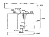
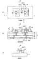
本発明の実施形態を説明する前に、本発明に関連する関連技術の問題点について説明する。図1は関連技術の実装用ソケットを使用して半導体パッケージをマザーボードに実装する様子を示す断面図である。
(Related technology)
Prior to describing embodiments of the present invention, problems of related technologies related to the present invention will be described. FIG. 1 is a cross-sectional view showing a state in which a semiconductor package is mounted on a mother board using a mounting socket according to related art.
図1に示すように、関連技術の実装用ソケット100では、樹脂製の筺体200にその厚み方向に貫通する穴220が設けられている。筺体200は樹脂を射出成型することにより作成される。
As shown in FIG. 1, in the
そして、筺体200の穴220の側面のスリット(不図示)にスプリング300の側部320が差し込まれて固定されている。スプリング300は筺体200の上面から上側に突出する突出接続部340を備えている。また、スプリング300は筺体200の穴220の下部に下側接続部360を備えている。
And the side part 320 of the spring 300 is inserted and fixed to the slit (not shown) of the side surface of the
実装用ソケット100の下側接続部360がはんだボール440を介してマザーボード400の接続電極420に接続される。さらに、実装用ソケット100の突出接続部340に、LGA型の半導体パッケージ500の接続パッド520(ランド)が配置される。
The
そして、半導体パッケージ500は不図示の押えキャップによって実装用ソケット100側に押圧されることにより、半導体パッケージ500の接続パッド520が実装用ソケット200を介してマザーボード400に導通する。
Then, the
関連技術の実装用ソケット100では、スプリング300が複雑な形状であるため、高度な加工技術が必要であり、作成にあたりかなりの手番を必要とする問題がある。
In the
また、筺体200を貫通する穴220の側方のスリットに縦型のスプリング300を差し込んで上下導通させるので、筺体200の上下面側でピッチ変換することは困難である。
In addition, since the vertical spring 300 is inserted into the slit on the side of the
さらには、筺体200の各穴220(径:600μm程度)の側方にスプリング300を差し込むための領域をそれぞれ確保する必要があることから、穴220の配置ピッチが比較的大きくなり(配置ピッチ:1.3mm程度)、小型化(高密度化)の要求に容易に対応できない問題がある。
Furthermore, since it is necessary to secure a region for inserting the spring 300 to the side of each hole 220 (diameter: about 600 μm) of the
しかも、筺体200はある程度の厚み(例えば2〜3mm)が必要で、スプリング300の突出接続パッド340の高さも比較的高く設定されるため、薄型化の要求に容易に対応できない問題がある。
In addition, the
以下に説明する本発明の実施形態の電気コネクタは、前述した不具合を解消することができる。 The electrical connector according to the embodiment of the present invention described below can solve the above-described problems.
(第1の実施の形態)
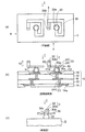
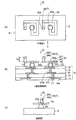
図2(a)は本発明の第1実施形態の電気コネクタを示す平面図、図2(b)は図2(a)の電気コネクタをA方向からみた透視側面図、図2(c)は図2(a)の電気コネクタをB方向からみた側面図、図3は図2(b)の電気コネクタを使用して実装基板に半導体パッケージを実装する様子を示す断面図である。
(First embodiment)
2A is a plan view showing the electrical connector according to the first embodiment of the present invention, FIG. 2B is a perspective side view of the electrical connector of FIG. 2A viewed from the direction A, and FIG. FIG. 2A is a side view of the electrical connector of FIG. 2A viewed from the B direction, and FIG. 3 is a cross-sectional view showing a state where a semiconductor package is mounted on a mounting board using the electrical connector of FIG.
図2(a)及び(b)に示すように、本発明の第1実施形態の電気コネクタ1(実装用ソケット)は、配線基板5と、配線基板5に接続されたバンプ電極20と、バンプ電極20に接続されたスプリング電極30とを備えている。
2A and 2B, the electrical connector 1 (mounting socket) according to the first embodiment of the present invention includes a
配線基板5では、第1絶縁層10の下面に下側接続パッドC1が形成されている。第1絶縁層10の下面には、下側接続パッドC1の上に開口部14aが設けられたソルダレジスト14が形成されている。第1絶縁層10には下側接続パッドC1に接続される第1ビアホールVH1が設けられている。
In the
また、第1絶縁層10の上には第1ビアホールVH1(ビア導体)を介して下側接続パッドC1に電気接続される内部配線層Wが形成されている。内部配線層Wの上には第2絶縁層12が形成されている。第2絶縁層12には内部配線層Wに接続される第2ビアホールVH2が形成されている。
Further, an internal wiring layer W that is electrically connected to the lower connection pad C1 through the first via hole VH1 (via conductor) is formed on the first insulating
さらに、第2絶縁層12の上には、第2ビアホールVH2(ビア導体)を介して内部配線層Wに接続される上側接続パッドC2が形成されている。第2絶縁層12の上には上側接続パッドC2の上に開口部16aが設けられたソルダレジスト16が形成されている。
Further, on the second insulating
下側接続パッドC1及び上側接続パッドC2は島状に配置されていてもよく、あるいは、配線層に繋がってその一端に配置されていてもよい。また、下側接続パッドC1及び上側接続パッドC2の表面にニッケル/金めっき層などのコンタクト層が設けられていてもよい。 The lower connection pad C1 and the upper connection pad C2 may be arranged in an island shape, or may be arranged at one end thereof connected to the wiring layer. Further, a contact layer such as a nickel / gold plating layer may be provided on the surfaces of the lower connection pad C1 and the upper connection pad C2.
第1、第2絶縁層10,12はエポキシやポリイミドなどの絶縁樹脂から形成され、下側接続パッドC1、内部配線層W及び上側接続パッドC2は銅などから形成される。配線層の積層数は任意に設定することができる。
The first and second insulating
そして、配線基板5の上側接続パッドC2上にはそれに接続されたバンプ電極20が形成されている。バンプ電極20は配線基板5のソルダレジスト16から上側に突出して形成されている。バンプ電極20は、銅ボール22とその外面を被覆するはんだ層24とにより構成される。バンプ電極20は外面にはんだ層24が設けられて上下側が導通できればよく、銅ボール22の代わりに樹脂ボールを使用し、樹脂ボールとその外面を被覆するはんだ層24とから構成してもよい。
A
さらに、配線基板5に形成されたバンプ電極20にはスプリング電極30が接続されている。図2(a)及び(b)に注目すると、スプリング電極30は、帯状金属板材がバンプ電極20の上から外側水平方向に向かって平面的に巻回されて形成されている。スプリング電極30の巻回方向の始端部30aがバンプ電極20に接続されて固定されており、始端部30a以外の部分は配線基板5から浮いた状態で配置されている。
Further, a
スプリング電極30は、リン青銅やベリリウム銅などの銅合金からなる。そのような金属板材は、良好な導電性と適度なスプリング(ばね)性を有する。
The
図2(a)の例では、スプリング電極30は反時計回りの方向に巻かれているが、時計方向に巻かれていてもよい。また、スプリング電極30はバンプ電極20の周囲に1回の巻き回数で巻かれているが、巻き回数は任意に設定できる。また、スプリング電極30は四角状に巻かれているが、円状などの各種の巻き形状を採用することができる。
In the example of FIG. 2A, the
さらに、図2(c)に注目すると、スプリング電極30の巻回方向の終端側には、本体部から上側に屈曲して延在する立上り部30cと、立上り部30cから水平方向に屈曲して延在する終端部30bとが設けられている。立上り部30cは、上側に向かって延在していればよく、図2(c)のように斜め上方向に向かって延在していてもよいし、垂直方向に向かって延在していてもよい。
2C, on the end side in the winding direction of the
そして、スプリング電極30の終端部30bの上に金層32(コンタクト層)が設けられて接触部Tが構成されている。
Then, a gold layer 32 (contact layer) is provided on the
コンタクト層として金層32を例示するが他の金属材料を使用してもよい。また、コンタクト層が不要な場合は、金層32を省略してスプリング電極30の終端部30bをそのまま接触部Tとして使用してもよい。
Although the
このように、第1実施形態の電気コネクタ1のスプリング電極30は、その終端側の2箇所が屈曲されて、終端部30bに始端部30bより高さの高い接触部Tを備えている。スプリング電極30の接触部Tはバンプ電極20の高さより高い位置に配置される。
As described above, the
本実施形態の電気コネクタ1のスプリング電極30を作成するには、まず、金属板材をプレス加工で打ち抜くことにより、スプリング電極30の型に巻回された帯状金属板材を作成する(第1工程)。さらに、巻回された帯状金属板材の終端側を曲げ加工することにより、本体部から上側に突出する終端部30bを得る(第2工程)。
In order to create the
このように、本実施形態の電気コネクタ1のスプリング電極30は、関連技術の複雑な形状のスプリングを作成する場合に比べて、極めて簡易な方法で作成することができ、加工手番を大幅に短縮することができる。
As described above, the
スプリング電極30の終端部30b上に金層32を形成する方法としては、金属板材を打ち抜く前に、金属板材の終端部30bになる部分に開口部が設けられためっきレジストを形成する。さらに、めっきレジストの開口部に電解めっき又は無電解めっきによって金層32を形成した後に、めっきレジストを除去する。
As a method of forming the
また、スプリング電極30を配線基板5に接続するには、まず、スプリング電極30を治具に配置し、配線基板5の上側接続パッドC2に仮接着されたはんだボール(表面のみがはんだ)を下側にして、はんだボールをスプリング電極30の始端部30aに配置する。さらに、加熱処理によってリフローはんだ付けを行うことにより、スプリング電極30がバンプ電極20によって配線基板5の上側接続パッドC2に固定される。
In order to connect the
なお、はんだリフローによってバンプ電極20の高さが低くなったり、ばらついたりすることを防止するため、前述した外面にはんだ層24が被覆された銅ボール22(又は樹脂ボール)を使用することが好ましい。バンプ電極20の高さ精度が問題にならない場合は、全体にわたってはんだからなるはんだボールを使用することも可能である。
In order to prevent the
後述するように、本実施形態の電気コネクタ1では、スプリング電極30の接触部Tに半導体パッケージの接続パッドが配置され、半導体パッケージが押えキャップによって電気コネクタ1側に押圧される。このとき、スプリング電極30の弾性機能によってスプリング電極30が下側に押し込まれる。これにより、半導体パッケージの接続パッドが電気コネクタ1の接触部Tに確実に導通するようになっている。
As will be described later, in the
例えば、半導体パッケージを実装する際のスプリング電極30の押し込み量を300μm程度と設定する場合、配線基板5の上面からスプリング電極30の下面までの隙間h1(バンプ電極20の高さ−ソルダレジスト16の厚み)(図2(b))は500μm程度に設定され、スプリング電極30の接触部Tの始端部30aからの突出高さh2(図2(b))は500μm程度に設定される。
For example, when the pushing amount of the
このように、スプリング電極30の接触部Tの突出高さh2を、半導体パッケージを接続する際のスプリング電極30の押し込み量より高く設定することにより、半導体パッケージがバンプ電極20上のスプリング電極30に干渉するおそれがない。
Thus, by setting the protruding height h2 of the contact portion T of the
さらに、配線基板5からスプリング電極30までの隙間h1を、半導体パッケージを接続する際のスプリング電極30の押し込み量より高くすることにより、スプリング電極30が配線基板5に干渉するおそれがない。
Furthermore, the gap h1 from the
本実施形態の電気コネクタ1では、配線基板5の上にバンプ電極20を介してスプリング電極30を設けている。配線基板5を使用することにより、内部配線層Wによって上側接続パッドC2と下側接続パッドC1との間でそれらの配置ピッチを任意に変換することができる。
In the
図2(b)の例では、下側接続パッドC1の配置ピッチが上側接続パッドC2の配置ピッチより大きくなるようにピッチ変換がなされている。これにより、関連技術と違って、狭小ピッチの接続パッドを備えた高性能な半導体パッケージであっても、本実施形態の電気コネクタを使用することにより実装基板の接続パッドに容易にピッチ変換することが可能になる。 In the example of FIG. 2B, the pitch conversion is performed so that the arrangement pitch of the lower connection pads C1 is larger than the arrangement pitch of the upper connection pads C2. As a result, unlike the related art, even a high-performance semiconductor package having a connection pad with a narrow pitch can be easily converted into a connection pad on the mounting board by using the electrical connector of this embodiment. Is possible.
また、関連技術と違って、複雑な形状のスプリングを筺体の穴の側方に差し込む必要がないので、各スプリング電極30の間隔を100μm程度に狭くすることができる。これにより、図2(a)においてスプリング電極30の幅を100μm程度とする場合は、配置ピッチが600μm程度になって高密度化を図ることができるので、高性能な電気コネクタとして構成することができる。
Further, unlike the related art, since it is not necessary to insert a spring having a complicated shape into the side of the hole in the housing, the interval between the
しかも、半導体パッケージを接続する際の押し込み量を考慮してスプリング電極30の接触部Tの突出高さやバンプ電極20の高さを設定できるので、配線基板5からのスプリング電極30の高さを必要最小限に設定することができる。
In addition, the protrusion height of the contact portion T of the
さらには、スプリング電極30の支持体として配線基板5を使用しているので、ビルドアップ配線技術を使用することにより薄型化が可能になる(厚み:200μm〜1mm)。これにより、関連技術より電気コネクタの薄型化(低背化)を図ることができる。
Furthermore, since the
次に、本実施形態の電気コネクタ1を使用して、実装基板に半導体パッケージを実装する方法について説明する。
Next, a method for mounting a semiconductor package on a mounting board using the
図3に示すように、まず、上面側に接続電極62を備えた実装基板60(マザーボード)を用意する。さらに、実装基板60の接続電極62にはんだボール64を介して本実施形態の電気コネクタ1の下側接続パッドC1を配置し、加熱処理によってリフローはんだ付けすることにより電気接続する。
As shown in FIG. 3, first, a mounting substrate 60 (motherboard) having a
さらに、半導体パッケージ6(半導体装置)を用意する。半導体パッケージ6は配線基板40の上に半導体チップ50が実装されて基本構成される。配線基板40では上面側にチップ用接続パッド42が設けられ、下面側に外部接続パッド44が設けられている。配線基板40の両面側には、チップ用接続パッド42及び外部接続パッド44の上に開口部46aが設けられたソルダレジスト46がそれぞれ形成されている。
Further, a semiconductor package 6 (semiconductor device) is prepared. The
配線基板40の内部には、チップ用接続パッド42及び外部接続パッド44に接続される内部配線層(不図示)が設けられている。そして、配線基板40のチップ用接続パッド42に半導体チップ50が接続バンプ52によってフリップチップ接続されている。さらに、半導体チップ50の下側の隙間にアンダーフィル樹脂54が充填されている。
Inside the
半導体チップ50の全体がモールド樹脂で封止されていてもよい。あるいは、配線基板40の上にフェイスアップで実装された半導体チップがワイヤによって配線基板のチップ用接続パッド42に接続され、半導体チップが樹脂封止されていてもよく、各種の実装方式を採用できる。
The entire semiconductor chip 50 may be sealed with a mold resin. Alternatively, the semiconductor chip mounted face up on the
このように、本実施形態で使用する半導体パッケージ6は外部接続方式がLGA(Land Grid Array)型であり、バンプレスの外部接続パッド44(ランド)を備えている。
As described above, the
そして、半導体パッケージ6の外部接続パッド44(ランド)を電気コネクタ1のスプリング電極30の接触部Tに配置する。電気コネクタ1のスプリング電極30の接触部Tは、半導体パッケージ6の外部接続パッド44に対応して設けられている。
Then, the external connection pad 44 (land) of the
さらに、電気コネクタ1に連結される押えキャップ56で半導体パッケージ6を押圧する。これにより、スプリング電極30が下側に押し込まれ、スプリング電極30の上側に戻ろうとする弾性力によって半導体パッケージ6の外部接続パッド44がスプリング電極30の接触部Tに確実に接触して導通する。
Further, the
前述したように、電気コネクタ1のスプリング電極30の接触部Tの突出高さh2(図2(b))及び配線基板5とスプリング電極30との隙間h1(図2(b))は、スプリング電極30の押し込み量より高く設定されている。
As described above, the protrusion height h2 (FIG. 2B) of the contact portion T of the
これにより、図3に示すように、半導体パッケージ6がバンプ電極20上のスプリング電極30に干渉するおそれがないと共に、スプリング電極30が配線基板5に干渉するおそれもない。
Thereby, as shown in FIG. 3, there is no possibility that the
このようにして、狭小ピッチの外部接続パッド44を備えた高性能な半導体パッケージ6が電気コネクタ1を介して実装基板60に信頼性よく電気接続される。故障などで半導体パッケージ6の取り外しが必要な場合は、押えキャップ56を取り外すことにより電気コネクタ1のスプリング電極30がその弾性機能によって元の位置に戻り、半導体パッケージ5を電子コネクタ1から容易に取り外すことができる。
In this way, the high-
(第2の実施の形態)
図4(a)は本発明の第2実施形態の電気コネクタを示す平面図、図4(b)は図4(a)の電気コネクタをA方向からみた透視側面図、図4(c)は図4(a)の電気コネクタをB方向からみた側面図である。第2実施形態では、第1実施形態と同一要素については同一符号を付してその説明を省略する。
(Second Embodiment)
4A is a plan view showing the electrical connector of the second embodiment of the present invention, FIG. 4B is a perspective side view of the electrical connector of FIG. 4A viewed from the direction A, and FIG. It is the side view which looked at the electrical connector of Fig.4 (a) from the B direction. In the second embodiment, the same elements as those in the first embodiment are denoted by the same reference numerals and description thereof is omitted.
図4(a)〜(c)に示すように、第2実施形態の電気コネクタ1aと第1実施形態の電気コネクタ1と違いは、スプリング電極30の終端側が屈曲しておらず、全体にわたって平坦で同一の高さ位置に配置されている。
As shown in FIGS. 4A to 4C, the difference between the
さらに、図4(b)に示すように、スプリング電極30の巻回方向の終端部30bの上にボール電極34が形成されて接触部Tが構成されている。このようにして、スプリング電極30は終端部30bに始端部30aより高さの高い接触部Tを備えている。スプリング電極30の接触部Tはバンプ電極20の高さより高い位置に配置される。
Further, as shown in FIG. 4B, the
接触部Tを構成するボール電極34は銅ボール34aとその外面を被覆する金層34b(コンタクト層)とにより構成される。銅ボール34aの代わりに樹脂ボールを使用し、樹脂ボールとその外面を被覆する金層34bとからボール電極34を構成してもよい。
The ball electrode 34 constituting the contact portion T is composed of a
ボール電極34は、はんだなどの導電性接着材35によってスプリング電極30の終端部30bに接合される。その他の構成は第1実施形態の図2と同一である。
The
接触部Tを構成するボール電極34が設けられたスプリング電極30を作成するには、金属板材を打ち抜くことによりスプリング電極30の型の巻回状の帯状金属部材を作成した後に、終端部30bになる部分にボール電極34を接合する。その後に、個々のスプリング電極30が得られるように金属板材を分離する。
In order to create the
第2実施形態においても、第1実施形態の図3と同様に、半導体パッケージ6の外部接続パッド44で電気コネクタ1aのスプリング電極30の接触部T(ボール電極34)を下側に押し込むことにより、両者を確実に導通させることができる。
Also in the second embodiment, similarly to FIG. 3 of the first embodiment, the contact portion T (ball electrode 34) of the
第1実施形態と同様に、電気コネクタ1aのスプリング電極30の接触部T(ボール電極34)の突出高さh2(図4(b))及び配線基板5とスプリング電極30との隙間h1(図4(b))は、スプリング電極30の押し込み量より高く設定されている。
Similar to the first embodiment, the protrusion height h2 (FIG. 4B) of the contact portion T (ball electrode 34) of the
これにより、半導体パッケージ6がバンプ電極20上のスプリング電極30に干渉するおそれがないと共に、スプリング電極30が配線基板5に干渉するおそれもない。
Thereby, there is no possibility that the
第2実施形態の電気コネクタ1aは第1実施形態と同様な効果を奏する。
The
(第3の実施の形態)
図5(a)は本発明の第3実施形態の電気コネクタを示す平面図、図5(b)は図5(a)の電気コネクタをA方向からみた透視側面図、図5(c)は図5(a)の電気コネクタをB方向からみた側面図である。第3実施形態では、第1実施形態と同一要素については同一符号を付してその説明を省略する。
(Third embodiment)
5A is a plan view showing an electrical connector according to a third embodiment of the present invention, FIG. 5B is a transparent side view of the electrical connector of FIG. 5A viewed from the direction A, and FIG. It is the side view which looked at the electrical connector of Fig.5 (a) from the B direction. In the third embodiment, the same elements as those in the first embodiment are denoted by the same reference numerals, and description thereof is omitted.
図5(a)〜(c)に示すように、第3実施形態の電気コネクタ1bと第1実施形態の電気コネクタ1との違いは、スプリング電極30の終端側が屈曲しておらず、全体にわたって平坦で同一の高さ位置に配置されている。
As shown in FIGS. 5A to 5C, the difference between the
さらに、図5(b)に示すように、スプリング電極30の巻回方向の終端部30bの上に金バンプ36(コンタクト層)が形成されて接触部Tが構成されている。このようにして、スプリング電極30はその終端部30bに始端部30aより高さの高い接触部Tを備えている。スプリング電極30の接触部Tはバンプ電極20の高さより高い位置に配置される。その他の構成は第1実施形態の図2と同一である。
Further, as shown in FIG. 5B, a gold bump 36 (contact layer) is formed on the
接触部Tを構成する金バンプ36が設けられたスプリング電極30を作成するには、金属板材を打ち抜くことによりスプリング電極30の型の巻回状の帯状金属部材を作成した後に、終端部30bになる部分にワイヤボンディング法(ワイヤバンプ法ともいう)に基づいて金バンプ36を形成する。
In order to create the
つまり、終端部32bになる部分に溶融した金ボールを超音波併用熱圧着により接合した後に、クランパを閉じて金ボールの直上でワイヤを切断して金バンプ36を形成する。その後に、個々のスプリング電極30が得られるように金属板材を分離する。
In other words, after the molten gold ball is joined to the end portion 32b by thermocompression bonding with ultrasonic waves, the clamper is closed and the wire is cut immediately above the gold ball to form the
第3実施形態においても、第1実施形態の図3と同様に、半導体パッケージ6の外部接続パッド44で電気コネクタ1bのスプリング電極30の接触部T(金バンプ36)を下側に押し込むことにより、両者を確実に導通させることができる。
Also in the third embodiment, as in FIG. 3 of the first embodiment, the contact portion T (gold bump 36) of the
第1実施形態と同様に、電気コネクタ1bのスプリング電極30の接触部T(金バンプ36)の突出高さh2(図5(b))及び配線基板5とスプリング電極30との隙間h1(図5(b))は、スプリング電極30の押し込み量より高く設定されている。
Similar to the first embodiment, the protruding height h2 (FIG. 5B) of the contact portion T (gold bump 36) of the
これにより、半導体パッケージ6がバンプ電極20上のスプリング電極30に干渉するおそれがないと共に、スプリング電極30が配線基板5に干渉するおそれもない。
Thereby, there is no possibility that the
第3実施形態の電気コネクタ1bは第1実施形態と同様な効果を奏する。
The
(第4の実施の形態)
図6(a)は本発明の第4実施形態の電気コネクタを示す平面図、図6(b)は図6(a)の電気コネクタをA方向からみた透視側面図、図6(c)は図6(a)の電気コネクタをB方向からみた側面図である。第4実施形態では、第1実施形態と同一要素については同一符号を付してその説明を省略する。
(Fourth embodiment)
6A is a plan view showing an electrical connector according to a fourth embodiment of the present invention, FIG. 6B is a perspective side view of the electrical connector of FIG. 6A viewed from the direction A, and FIG. It is the side view which looked at the electrical connector of Fig.6 (a) from the B direction. In the fourth embodiment, the same elements as those in the first embodiment are denoted by the same reference numerals, and the description thereof is omitted.
図6(a)〜(c)に示すように、第4実施形態の電気コネクタ1cと第1実施形態の電気コネクタ1との違いは、スプリング電極30の終端側が屈曲しておらず、全体にわたって平坦で同一の高さ位置に配置されている。
As shown in FIGS. 6A to 6C, the difference between the
さらに、図6(b)に示すように、スプリング電極30の巻回方向の終端部30bの上に金属めっき柱38が形成されて接触部Tが構成されている。このようにして、スプリング電極30はその終端部30bに始端部30aより高さの高い接触部Tを備えている。スプリング電極30の接触部Tはバンプ電極20の高さより高い位置に配置される。
Further, as shown in FIG. 6B, a
金属めっき柱38は、下から順に、銅めっき層38a及び金めっき層38b(コンタクト層)から構成される。その他の構成は第1実施形態の図2と同一である。
The
接触部Tを構成する金属めっき柱38が設けられたスプリング電極30を形成するには、まず、金属板材を打ち抜くことによりスプリング電極30の型の巻回状の帯状金属部材を作成した後に、終端部30bになる部分に開口部が設けられためっきレジストを形成する。次いで、めっきレジストの開口部内の深さ方向の主要部に電解めっきにより銅めっき層38aを形成し、その上部に金めっき層38bを形成する。さらに、めっきレジストを除去した後に、個々のスプリング電極30が得られるように金属板材を分離する。
In order to form the
第4実施形態においても、第1実施形態の図3と同様に、半導体パッケージ6の外部接続パッド44で電気コネクタ1cのスプリング電極30の接触部T(金属めっき柱38)を下側に押し込むことにより、両者を確実に導通させることができる。
Also in the fourth embodiment, as in FIG. 3 of the first embodiment, the contact portion T (metal plating column 38) of the
第1実施形態と同様に、電気コネクタ1cのスプリング電極30の接触部T(金属めっき柱38)の突出高さh2(図6(b))及び配線基板5とスプリング電極30との隙間h1(図6(b))は、スプリング電極30の押し込み量より高く設定されている。
Similar to the first embodiment, the protrusion height h2 (FIG. 6B) of the contact portion T (metal plating column 38) of the
これにより、半導体パッケージ6がバンプ電極20上のスプリング電極30に干渉するおそれがないと共に、スプリング電極30が配線基板5に干渉するおそれもない。
Thereby, there is no possibility that the
第4実施形態の電気コネクタ1cは第1実施形態と同様な効果を奏する。
The
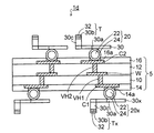
(第5の実施の形態)
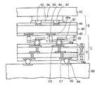
図7は本発明の第5実施形態の電気コネクタを示す断面図である。第5実施形態では、第1実施形態と同一要素については同一符号を付してその説明を省略する。
(Fifth embodiment)
FIG. 7 is a sectional view showing an electrical connector according to a fifth embodiment of the present invention. In the fifth embodiment, the same elements as those in the first embodiment are denoted by the same reference numerals and description thereof is omitted.
図7に示すように、第5実施形態の電気コネクタ1d(インターポーザ)では、第1実施形態の電気コネクタ1(図2)において、配線基板5の下面側の下側接続パッドC1にもバンプ電極20xを介して接触部Txを備えたスプリング電極30xが設けられている。配線基板5の下面側のバンプ電極20x及びスプリング電極30xの構成は、配線基板5の上面側のバンプ電極20及びスプリング電極30と同一である。
As shown in FIG. 7, in the
第5実施形態の電気コネクタ1dは配線基板5の両面側にスプリング電極30,30xが設けられているので、取り外し可能なインターポーザとして使用することができる。
Since the
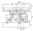
図8には、第5実施形態の電気コネクタ1dを使用して半導体ウェハの特性試験(バーンイン試験)を行う様子が示されている。
FIG. 8 shows a state where a semiconductor wafer characteristic test ( burn-in test) is performed using the
図8に示すように、半導体ウェハ70(シリコンウェハ)は個々の半導体チップを得るためのものであり、トランジスタ(半導体素子)、キャパシタ及び抵抗などの回路素子が形成された複数の素子形成領域Eが設けられている。半導体ウェハ70の素子形成面には接続パッド72が設けられている。
As shown in FIG. 8, a semiconductor wafer 70 (silicon wafer) is for obtaining individual semiconductor chips, and a plurality of element formation regions E in which circuit elements such as transistors (semiconductor elements), capacitors, and resistors are formed. Is provided.
各素子形成領域Eの上(図8では下)には、各種素子を接続するための多層配線(不図示)が形成されており、多層配線が接続パッド72に接続されている。さらに、半導体ウェハ70の素子形成面には接続パッド72上に開口部74aが設けられたパッシベーション膜74が形成されている。
A multilayer wiring (not shown) for connecting various elements is formed above each element formation region E (bottom in FIG. 8), and the multilayer wiring is connected to the
さらに、半導体ウェハ70の特性試験を行うための試験用配線基板80を用意する。試験用配線基板80の上面側には接続電極82が設けられている。試験用配線基板80には、半導体ウェハ70の特性試験を行うための電気回路が設けられている。
Further, a
そして、試験用配線基板80の接続電極82の上に、上記した第5実施形態の電気コネクタ1dの下面側のスプリング電極30xの接触部Txを配置する。さらに、電気コネクタ1dの上面側のスプリング電極30の接触部Tの上に、半導体ウェハ70の接続パッド72を配置する。
Then, on the
次いで、押えキャップ56で半導体ウェハ70を下側に押圧することにより、電気コネクタ1dの上面側のスプリング電極30が下側に押し込まれる。これにより、半導体ウェハ70の接続パッド72と電気コネクタ1dの上面側のスプリング電極30の接触部Tとが確実に導通する。
Next, by pressing the
また同時に、電気コネクタ1dの下面側のスプリング電極30xが上側に押し込まれて電気コネクタ1dの下面側のスプリング電極30xの接触部Txと試験用配線基板80の接続電極82とが確実に導通する。
At the same time, the
このようにして、半導体ウェハ70の接続パッド72のピッチが電気コネクタ1dによって試験用配線基板80の接続電極82のピッチに変換される。そして、半導体ウェハ70の各素子形成領域Eの特性試験が行われる。
In this way, the pitch of the
半導体ウェハ70の特性試験が終了した後に、押えキャップ56を取り外すことにより、電気コネクタ1dのスプリング電極30,30xがその弾性機能によって元の位置に戻る。その後に、半導体ウェハ70を電気コネクタ1dから取り外し、電気コネクタ1dを試験用配線基板80から取り外す。
After the characteristic test of the
第5実施形態の電気コネクタ1dは、第1実施形態と同様な効果を奏すると共に、取り外しが可能なインターポーザとして機能する。
The
前述した第2〜第4実施形態の電気コネクタ1a〜1cにおいても、同様に、配線基板5の下面側にもバンプ電極20xを介してスプリング電極30xを設けて、取り外しが可能なインターポーザとして使用してもよい。
Similarly, in the
1,1a〜1d…第1〜第5の電気コネクタ、5,40…配線基板、6…半導体パッケージ、10…第1絶縁層、12…第2絶縁層、14,16,46…ソルダレジスト、14a,16a,46a,74a…開口部、20,20x…バンプ電極、22,34a…銅ボール、24…はんだ層、30,30x…スプリング電極、30a…始端部、30b…終端部、32,34b…金層、34…ボール電極、36…金バンプ、38…金属めっき柱、42…チップ用接続パッド、44…外部接続パッド、50…半導体チップ、52…接続バンプ、54…アンダーフィル樹脂、56…押えキャップ、60…実装基板、62,82…接続電極、70…半導体ウェハ、72…接続パッド、74…パッシベーション膜、80…試験用配線基板、C1…下側接続パッド、C2…上側接続パッド、E…素子形成領域、T,Tx…接触部、W…内部配線層、VH1,VH2…ビアホール。
DESCRIPTION OF
Claims (10)
前記上側接続パッドの上に形成されたバンプ電極と、
前記バンプ電極の上から外側に向かって平面的に巻回して形成され、巻回方向の始端部が前記バンプ電極に接続され、前記巻回方向の終端部に前記始端部より高さの高い接触部を備えたスプリング電極とを有することを特徴とする電気コネクタ。 A wiring board having an upper connection pad on the upper surface side and a lower connection pad on the lower surface side;
A bump electrode formed on the upper connection pad;
Formed by winding the bump electrode from the top to the outside in a planar manner, the start end in the winding direction is connected to the bump electrode, and the end in the winding direction is higher in contact than the start end An electrical connector comprising: a spring electrode provided with a portion.
Priority Applications (1)
| Application Number | Priority Date | Filing Date | Title |
|---|---|---|---|
| JP2009262636A JP5367542B2 (en) | 2009-11-18 | 2009-11-18 | Electrical connector |
Applications Claiming Priority (1)
| Application Number | Priority Date | Filing Date | Title |
|---|---|---|---|
| JP2009262636A JP5367542B2 (en) | 2009-11-18 | 2009-11-18 | Electrical connector |
Publications (3)
| Publication Number | Publication Date |
|---|---|
| JP2011108504A JP2011108504A (en) | 2011-06-02 |
| JP2011108504A5 JP2011108504A5 (en) | 2012-09-20 |
| JP5367542B2 true JP5367542B2 (en) | 2013-12-11 |
Family
ID=44231757
Family Applications (1)
| Application Number | Title | Priority Date | Filing Date |
|---|---|---|---|
| JP2009262636A Active JP5367542B2 (en) | 2009-11-18 | 2009-11-18 | Electrical connector |
Country Status (1)
| Country | Link |
|---|---|
| JP (1) | JP5367542B2 (en) |
Family Cites Families (2)
| Publication number | Priority date | Publication date | Assignee | Title |
|---|---|---|---|---|
| JPH11149969A (en) * | 1997-11-13 | 1999-06-02 | Sony Corp | Socket for semiconductor device inspection equipment |
| JP2001093634A (en) * | 1999-09-21 | 2001-04-06 | Kato Spring Works Co Ltd | Socket for semiconductor package |
-
2009
- 2009-11-18 JP JP2009262636A patent/JP5367542B2/en active Active
Also Published As
| Publication number | Publication date |
|---|---|
| JP2011108504A (en) | 2011-06-02 |
Similar Documents
| Publication | Publication Date | Title |
|---|---|---|
| JP5500870B2 (en) | Substrate with connection terminal and socket for electronic parts | |
| US20070241463A1 (en) | Electrode, manufacturing method of the same, and semiconductor device having the same | |
| CN104685622B (en) | BVA intermediary agent structures | |
| JP5713598B2 (en) | Socket and manufacturing method thereof | |
| JP5661225B2 (en) | Semiconductor device packaging method | |
| JP5606695B2 (en) | Board with connection terminal | |
| US6943100B2 (en) | Method of fabricating a wiring board utilizing a conductive member having a reduced thickness | |
| US8890337B1 (en) | Column and stacking balls package fabrication method and structure | |
| JP5341337B2 (en) | Semiconductor device and manufacturing method thereof | |
| JP5788166B2 (en) | Connection terminal structure, manufacturing method thereof, and socket | |
| JP2006186321A (en) | Circuit board manufacturing method and electronic component mounting structure manufacturing method | |
| JP4494175B2 (en) | Semiconductor device | |
| CN101330071A (en) | Mounting substrate and manufacturing method thereof | |
| JP4489575B2 (en) | Semiconductor device and manufacturing method thereof | |
| JP2011014944A (en) | Method of manufacturing electronic parts packaging structure | |
| US20080290528A1 (en) | Semiconductor package substrate having electrical connecting pads | |
| JP2008147598A (en) | Stacked package and manufacturing method thereof | |
| JP2002368155A (en) | Wiring board, semiconductor device, and method of manufacturing wiring board | |
| JP5367542B2 (en) | Electrical connector | |
| KR20110017153A (en) | Ball Grid Array Package Substrate and Manufacturing Method Thereof | |
| CN101958292B (en) | Printed circuit board, encapsulation piece and manufacture methods thereof | |
| CN102280428A (en) | Packaging piece and manufacture method thereof | |
| CN102034786A (en) | Printed circuit board, stud grid array package and manufacturing method thereof | |
| KR101534849B1 (en) | Flip chip package and method of manufacturing the same | |
| TWI581388B (en) | Semiconductor package structure |
Legal Events
| Date | Code | Title | Description |
|---|---|---|---|
| A521 | Written amendment |
Free format text: JAPANESE INTERMEDIATE CODE: A523 Effective date: 20120806 |
|
| A621 | Written request for application examination |
Free format text: JAPANESE INTERMEDIATE CODE: A621 Effective date: 20120806 |
|
| A977 | Report on retrieval |
Free format text: JAPANESE INTERMEDIATE CODE: A971007 Effective date: 20130725 |
|
| TRDD | Decision of grant or rejection written | ||
| A01 | Written decision to grant a patent or to grant a registration (utility model) |
Free format text: JAPANESE INTERMEDIATE CODE: A01 Effective date: 20130903 |
|
| A61 | First payment of annual fees (during grant procedure) |
Free format text: JAPANESE INTERMEDIATE CODE: A61 Effective date: 20130911 |
|
| R150 | Certificate of patent or registration of utility model |
Ref document number: 5367542 Country of ref document: JP Free format text: JAPANESE INTERMEDIATE CODE: R150 Free format text: JAPANESE INTERMEDIATE CODE: R150 |