JP5674096B2 - Photoelectric conversion cell and array, and reading method and circuit thereof - Google Patents
Photoelectric conversion cell and array, and reading method and circuit thereof Download PDFInfo
- Publication number
- JP5674096B2 JP5674096B2 JP2010164791A JP2010164791A JP5674096B2 JP 5674096 B2 JP5674096 B2 JP 5674096B2 JP 2010164791 A JP2010164791 A JP 2010164791A JP 2010164791 A JP2010164791 A JP 2010164791A JP 5674096 B2 JP5674096 B2 JP 5674096B2
- Authority
- JP
- Japan
- Prior art keywords
- semiconductor region
- photoelectric conversion
- potential
- cell
- output
- Prior art date
- Legal status (The legal status is an assumption and is not a legal conclusion. Google has not performed a legal analysis and makes no representation as to the accuracy of the status listed.)
- Expired - Fee Related
Links
- 238000006243 chemical reaction Methods 0.000 title claims description 464
- 238000000034 method Methods 0.000 title description 13
- 239000004065 semiconductor Substances 0.000 claims description 582
- 230000005669 field effect Effects 0.000 claims description 61
- 230000003321 amplification Effects 0.000 claims description 22
- 239000012535 impurity Substances 0.000 claims description 22
- 238000003199 nucleic acid amplification method Methods 0.000 claims description 22
- 230000007704 transition Effects 0.000 claims description 20
- 230000000694 effects Effects 0.000 claims description 12
- 230000015572 biosynthetic process Effects 0.000 claims description 2
- 230000000903 blocking effect Effects 0.000 claims description 2
- 239000010408 film Substances 0.000 description 52
- 230000008859 change Effects 0.000 description 29
- 238000010586 diagram Methods 0.000 description 15
- 239000000758 substrate Substances 0.000 description 12
- 125000004429 atom Chemical group 0.000 description 11
- 238000005513 bias potential Methods 0.000 description 10
- 238000007667 floating Methods 0.000 description 10
- 238000003491 array Methods 0.000 description 9
- 238000004519 manufacturing process Methods 0.000 description 9
- 230000035945 sensitivity Effects 0.000 description 9
- XUIMIQQOPSSXEZ-UHFFFAOYSA-N Silicon Chemical compound [Si] XUIMIQQOPSSXEZ-UHFFFAOYSA-N 0.000 description 7
- 238000002955 isolation Methods 0.000 description 7
- 229910052710 silicon Inorganic materials 0.000 description 7
- 239000010703 silicon Substances 0.000 description 7
- 239000000969 carrier Substances 0.000 description 6
- 230000007423 decrease Effects 0.000 description 6
- 238000009792 diffusion process Methods 0.000 description 6
- 238000000926 separation method Methods 0.000 description 5
- 101100255205 Caenorhabditis elegans rsa-2 gene Proteins 0.000 description 4
- 238000001514 detection method Methods 0.000 description 4
- 230000003287 optical effect Effects 0.000 description 4
- 230000008569 process Effects 0.000 description 4
- 229920006395 saturated elastomer Polymers 0.000 description 4
- 101000590492 Homo sapiens Nuclear fragile X mental retardation-interacting protein 1 Proteins 0.000 description 3
- 102100032428 Nuclear fragile X mental retardation-interacting protein 1 Human genes 0.000 description 3
- 101150024161 RSB1 gene Proteins 0.000 description 3
- 238000005286 illumination Methods 0.000 description 3
- 230000002093 peripheral effect Effects 0.000 description 3
- 230000009467 reduction Effects 0.000 description 3
- 230000001052 transient effect Effects 0.000 description 3
- 238000009825 accumulation Methods 0.000 description 2
- 230000015556 catabolic process Effects 0.000 description 2
- 238000010168 coupling process Methods 0.000 description 2
- 238000005859 coupling reaction Methods 0.000 description 2
- 238000005516 engineering process Methods 0.000 description 2
- 230000006872 improvement Effects 0.000 description 2
- 238000005259 measurement Methods 0.000 description 2
- 230000002265 prevention Effects 0.000 description 2
- 230000000630 rising effect Effects 0.000 description 2
- 239000010409 thin film Substances 0.000 description 2
- 101150073536 FET3 gene Proteins 0.000 description 1
- 206010034960 Photophobia Diseases 0.000 description 1
- 206010034972 Photosensitivity reaction Diseases 0.000 description 1
- 101100484930 Saccharomyces cerevisiae (strain ATCC 204508 / S288c) VPS41 gene Proteins 0.000 description 1
- VYPSYNLAJGMNEJ-UHFFFAOYSA-N Silicium dioxide Chemical compound O=[Si]=O VYPSYNLAJGMNEJ-UHFFFAOYSA-N 0.000 description 1
- 238000010521 absorption reaction Methods 0.000 description 1
- 230000009471 action Effects 0.000 description 1
- 230000003749 cleanliness Effects 0.000 description 1
- 230000000295 complement effect Effects 0.000 description 1
- 239000002131 composite material Substances 0.000 description 1
- 238000012937 correction Methods 0.000 description 1
- 230000008878 coupling Effects 0.000 description 1
- 230000003111 delayed effect Effects 0.000 description 1
- 238000013461 design Methods 0.000 description 1
- 230000009189 diving Effects 0.000 description 1
- 230000005684 electric field Effects 0.000 description 1
- 238000002474 experimental method Methods 0.000 description 1
- 125000005842 heteroatom Chemical group 0.000 description 1
- 238000012905 input function Methods 0.000 description 1
- 238000009413 insulation Methods 0.000 description 1
- 230000003993 interaction Effects 0.000 description 1
- 230000031700 light absorption Effects 0.000 description 1
- 208000013469 light sensitivity Diseases 0.000 description 1
- 238000001459 lithography Methods 0.000 description 1
- 239000002184 metal Substances 0.000 description 1
- ORQBXQOJMQIAOY-UHFFFAOYSA-N nobelium Chemical compound [No] ORQBXQOJMQIAOY-UHFFFAOYSA-N 0.000 description 1
- 230000003071 parasitic effect Effects 0.000 description 1
- 238000002161 passivation Methods 0.000 description 1
- 230000036211 photosensitivity Effects 0.000 description 1
- 229910021420 polycrystalline silicon Inorganic materials 0.000 description 1
- 238000012545 processing Methods 0.000 description 1
- 238000010187 selection method Methods 0.000 description 1
- 229910052814 silicon oxide Inorganic materials 0.000 description 1
Images


Classifications
-
- H—ELECTRICITY
- H01—ELECTRIC ELEMENTS
- H01L—SEMICONDUCTOR DEVICES NOT COVERED BY CLASS H10
- H01L27/00—Devices consisting of a plurality of semiconductor or other solid-state components formed in or on a common substrate
- H01L27/14—Devices consisting of a plurality of semiconductor or other solid-state components formed in or on a common substrate including semiconductor components sensitive to infrared radiation, light, electromagnetic radiation of shorter wavelength or corpuscular radiation and specially adapted either for the conversion of the energy of such radiation into electrical energy or for the control of electrical energy by such radiation
- H01L27/144—Devices controlled by radiation
- H01L27/146—Imager structures
- H01L27/14601—Structural or functional details thereof
- H01L27/14609—Pixel-elements with integrated switching, control, storage or amplification elements
-
- H—ELECTRICITY
- H01—ELECTRIC ELEMENTS
- H01L—SEMICONDUCTOR DEVICES NOT COVERED BY CLASS H10
- H01L27/00—Devices consisting of a plurality of semiconductor or other solid-state components formed in or on a common substrate
- H01L27/14—Devices consisting of a plurality of semiconductor or other solid-state components formed in or on a common substrate including semiconductor components sensitive to infrared radiation, light, electromagnetic radiation of shorter wavelength or corpuscular radiation and specially adapted either for the conversion of the energy of such radiation into electrical energy or for the control of electrical energy by such radiation
- H01L27/144—Devices controlled by radiation
- H01L27/1446—Devices controlled by radiation in a repetitive configuration
-
- H—ELECTRICITY
- H01—ELECTRIC ELEMENTS
- H01L—SEMICONDUCTOR DEVICES NOT COVERED BY CLASS H10
- H01L31/00—Semiconductor devices sensitive to infrared radiation, light, electromagnetic radiation of shorter wavelength or corpuscular radiation and specially adapted either for the conversion of the energy of such radiation into electrical energy or for the control of electrical energy by such radiation; Processes or apparatus specially adapted for the manufacture or treatment thereof or of parts thereof; Details thereof
- H01L31/08—Semiconductor devices sensitive to infrared radiation, light, electromagnetic radiation of shorter wavelength or corpuscular radiation and specially adapted either for the conversion of the energy of such radiation into electrical energy or for the control of electrical energy by such radiation; Processes or apparatus specially adapted for the manufacture or treatment thereof or of parts thereof; Details thereof in which radiation controls flow of current through the device, e.g. photoresistors
- H01L31/10—Semiconductor devices sensitive to infrared radiation, light, electromagnetic radiation of shorter wavelength or corpuscular radiation and specially adapted either for the conversion of the energy of such radiation into electrical energy or for the control of electrical energy by such radiation; Processes or apparatus specially adapted for the manufacture or treatment thereof or of parts thereof; Details thereof in which radiation controls flow of current through the device, e.g. photoresistors characterised by at least one potential-jump barrier or surface barrier, e.g. phototransistors
- H01L31/101—Devices sensitive to infrared, visible or ultraviolet radiation
- H01L31/102—Devices sensitive to infrared, visible or ultraviolet radiation characterised by only one potential barrier or surface barrier
- H01L31/103—Devices sensitive to infrared, visible or ultraviolet radiation characterised by only one potential barrier or surface barrier the potential barrier being of the PN homojunction type
-
- H—ELECTRICITY
- H04—ELECTRIC COMMUNICATION TECHNIQUE
- H04N—PICTORIAL COMMUNICATION, e.g. TELEVISION
- H04N25/00—Circuitry of solid-state image sensors [SSIS]; Control thereof
- H04N25/60—Noise processing, e.g. detecting, correcting, reducing or removing noise
- H04N25/63—Noise processing, e.g. detecting, correcting, reducing or removing noise applied to dark current
Description
本発明は光を電気信号へ変換する光電変換セルおよびそれを用いたアレイに関する。またそれらの読み出し技術に関する。 The present invention relates to a photoelectric conversion cell for converting light into an electric signal and an array using the photoelectric conversion cell. Further, the present invention relates to those reading techniques.
従来フォトトランジスタの2次元アレイから画素情報を読み出す場合には、図1に示すように画素としてのフォトトランジスタのエミッタをワード線に接続し、コレクタをビット線に接続して、コレクタに負荷抵抗を接続して負荷抵抗を接続されたコレクタの電位変化から画素情報を読み出していた(図1は非特許文献1のFig.5を引用)。コレクタ・ベース間容量と負荷抵抗で計算される読み出し時間の遅れが、コレクタ電位が出力信号により変化するためのミラー効果により増加する問題があった。さらに、コレクタと分離領域および基板との間の浮遊容量のためにも読み出し時間の遅れが生じた。コレクタと分離領域および基板との間に流れるリーク電流のために等価的にフォトトランジスタの暗電流が増加した。また1つのビット線に接続されている非選択フォトトランジスタのコレクタは選択
フォトトランジスタの読み出し時電圧変化がそのまま加わり、そのビット線に接続されている他のフォトトランジスタが読み出されるたびに擾乱を受けていた。このため、画素同士の情報相互干渉のない精度のよい検出、または低照度の情報検出には限界があった。
When reading pixel information from a conventional two-dimensional array of phototransistors, as shown in FIG. 1, the emitter of the phototransistor as a pixel is connected to the word line, the collector is connected to the bit line, and the load resistance is applied to the collector. The pixel information was read out from the potential change of the collector connected to the load resistor (FIG. 1 is cited from FIG. 5 of Non-Patent Document 1). There has been a problem that the delay in the readout time calculated by the collector-base capacitance and the load resistance increases due to the mirror effect for the collector potential to be changed by the output signal. In addition, the readout time is delayed due to the stray capacitance between the collector and the isolation region and the substrate. The dark current of the phototransistor increased equivalently due to the leakage current flowing between the collector and the isolation region and the substrate. The collector of the non-selected phototransistor connected to one bit line is subjected to a change in voltage when the selected phototransistor is read, and is disturbed each time another phototransistor connected to that bitline is read. It was. For this reason, there is a limit to accurate detection without information mutual interference between pixels or information detection with low illuminance.
更にこのようにコレクタを基板から分離する必要のある構造は、コレクタの深さ方向の厚さを充分大きく出来ないので、コレクタを形成する半導体のバンドギャップエネルギーに近い波長感度まで感度よく光電変換する事が、シリコンのように赤外領域の光吸収係数の小さい半導体では困難であった。 Furthermore, in such a structure that requires the collector to be separated from the substrate, the thickness in the depth direction of the collector cannot be increased sufficiently, so that photoelectric conversion is performed with high sensitivity to a wavelength sensitivity close to the band gap energy of the semiconductor forming the collector. This is difficult with a semiconductor having a small light absorption coefficient in the infrared region, such as silicon.
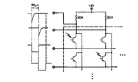
一方、図2に示すようにフォトトランジスタ1次元アレイ49の画素としてのフォトトランジスタの個々のコレクタをオン/オフするバイポーラトランジスタスイッチ1次元アレイ48の個々のコレクタに接続して1次元アレイ内で共通接続したフォトトランジスタのエミッタから光電流を読み出す1次元リニアセンサーアレイ技術は開示されていた(特許文献1の第5図を引用。なお、説明に不要な番号は削除した。)。この公知例ではフォトトランジスタのコレクタがオフ状態のスイッチに接続されているときはコレクタがフローティング電位状態となっており、これに他のフォトトランジスタのコレクタを接続するとフローティング電位が該他のフォトトランジスタの光情報の蓄積状態と相互作用して擾乱が発生するので、2次元アレイまで視野に入れていないこのアレイをあえて2次元アレイ化するためにこの1次元アレイの複数のコレクタを単に2次元に接続しただけでは画素の情報の相互作用のすくない2次元アレイは実現が難しい。
On the other hand, as shown in FIG. 2, a bipolar transistor switch for turning on / off individual collectors of the phototransistors as pixels of the phototransistor one-
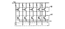
また、特許文献1には図3(特許文献1の第6図を引用。なお、説明に不要な番号は削除した。)に示すようにフォトトランジスタ1次元アレイ53の画素としてのフォトトランジスタの個々のエミッタをオン/オフするバイポーラトランジスタスイッチ1次元アレイの個々のコレクタに接続して1次元アレイ内で共通接続されたフォトトランジスタのコレクタから光電流を読み出す1次元リニアセンサーアレイ技術も開示されていた。この公知例ではもともと2次元アレイは視野に置かれていないが、フォトトランジスタのエミッタがオフ状態のスイッチに接続されているときはエミッタがフローティング電位状態となっており、2次元アレイを実現するためにあえてこれに他のフォトトランジスタのエミッタを接続するとフローティング電位が該他のフォトトランジスタの光情報の蓄積状態と相互作用して擾乱が発生するため、この1次元アレイの複数のエミッタを接続しただけでは画素の情報の相互作用のすくない2次元アレイは実現が難しい。
このように特許文献1の技術では2次元アレイを組んだとしても、画素情報同士の相互干渉
のために精度の高い、または低照度の画素情報検出には限度がある。
Further, in
As described above, even if a two-dimensional array is assembled in the technique of
更にコレクタに負荷を接続したり、コレクタを個別に駆動したり、行ないしは列毎に駆動したりするためにはコレクタを少なくとも行ないしは列毎に基板と分離する必要があり、このために、埋め込み層拡散、エピタキシアル成長、分離工程とMOSLSI製造工程と異質の工程が多く、番地選択など周辺回路をMOSLSIで製造する場合には製造工程の質、数ともに不利である。 Furthermore, in order to connect a load to the collector, to drive the collector individually, or to drive every row or column, it is necessary to separate the collector from the substrate at least every row or column. There are many different processes from layer diffusion, epitaxial growth, separation process and MOSLSI manufacturing process. When peripheral circuits such as address selection are manufactured by MOSLSI, both the quality and number of manufacturing processes are disadvantageous.
これにたいして、図4に示すように、個々のフォトトランジスタのベースと結合した電気容量を設けて画素とし、この電気容量を介してベースに印加されたパルスとエミッタ電位変化で番地選択を行い、フォトトランジスタのコレクタは共通電位としたアレイ構成が開示されていた(図4は非特許文献2のFig.1(a)を引用。)。しかし、この方法も1つの番地選択線へ上記電気容量が接続されている非選択画素すべてに擾乱が入ってしまう。したがって低照度画像信号の検出には限界がある。
このベースと結合した電気容量を設ける番地選択法は特許文献2の図1、図2、図3、図12、図17、図20、図21、図33にも開示されている。
On the other hand, as shown in FIG. 4, an electric capacity coupled with the base of each phototransistor is provided to form a pixel, and an address is selected by a pulse applied to the base via this electric capacity and a change in the emitter potential. An array configuration in which the collectors of the transistors are set to a common potential has been disclosed (see FIG. 1 (a) of Non-Patent
This address selection method for providing an electric capacity coupled to the base is also disclosed in FIGS. 1, 2, 3, 3, 12, 17, 20, 21, and 33 of
図5は特許文献3の第1図(説明に不要な番号等は削除した。)に開示されたフォトトランジスタ1次元アレイで、1次元アレイのフォトトランジスタ1a、1b、---、1fの各エミッタが読み出し用スイッチFET2a、2b、---、2fおよび充電用スイッチFET3a、3b、---、3fのドレインに接続されている。充電用スイッチFETのソースはまとめて再充電電圧VBBに接続されている。明細書2ページ左下欄の3〜5行では「再充電スイッチは読み出し終了後、1クロック時間またはそれ以上経過させる」と記載しているようにリニアセンサーでも1画素に2選択配線が必要になっている。
この公知例では画像信号出力端子4へFET2、FET3のゲートへ加える番地選択用パルス雑音がFETのゲート・ソース間キャパシタンスを通して画像信号と同符号で加わり、低照度画像信号は雑音に隠れてしまう。またこれを2次元アレイとするための接続ないしはFETの組み合わせ、配線は1画素あたり何本になるのか、再充電スイッチ動作フェーズ等開示されていない。この公知例でたとえ2次元アレイを組んだとしても番地選択雑音により低照度画像信号を検出する限界がある。
FIG. 5 is a one-dimensional phototransistor array disclosed in FIG. 1 of Patent Document 3 (numbers unnecessary for explanation are deleted). Each of the one-dimensional phototransistors 1a, 1b, ---, and 1f The emitters are connected to the drains of the readout switches FET2a, 2b, ---, 2f and the charging switches FET3a, 3b, ---, 3f. The sources of the charging switch FET are collectively connected to the recharging voltage VBB .
In this known example, address selection pulse noise applied to the gates of the FET2 and FET3 to the image
図6は特許文献4の第1図(説明に不要な番号は削除した。)に開示されたフォトトランジスタ1次元アレイで、各画素の選択にアナログスイッチを用いている。アナログスイッチはそのゲートに正方向へ遷移するパルスと負方向へ遷移するパルスの両方を印加する必要があり、読み出し信号と必ず同符号のパルス雑音がゲート・ソース間のキャパシタンスを通して画像信号と同符号で加わり、低照度信号は雑音に隠れてしまう。更に、信号出力線の電位が変化すると、画素内部の電位まで変化して、信号出力線に接続される回路の動作に制限を与えるだけでなく、信号出力線の雑音が画素に読み込まれてしまう。また、セルの選択に信号読み出し線のほかに画素ごとに2本の配線が必要となり、2次元アレイを組むことを視野には置いていない画素構成であるため2次元アレイのための画素構成としては不適切である。 FIG. 6 is a one-dimensional phototransistor array disclosed in FIG. 1 of Patent Document 4 (numbers unnecessary for explanation are deleted), and an analog switch is used to select each pixel. An analog switch must apply both positive and negative transition pulses to its gate, and the pulse noise of the same sign as the readout signal must be the same as the image signal through the gate-source capacitance. In addition, the low light signal is hidden in the noise. Furthermore, when the potential of the signal output line changes, it changes to the internal potential of the pixel, which not only restricts the operation of the circuit connected to the signal output line, but also causes noise in the signal output line to be read into the pixel. . In addition to the signal readout line for cell selection, two wires are required for each pixel, and since it is a pixel configuration that does not put the 2D array into view, it is a pixel configuration for a 2D array. Is inappropriate.
本発明は、上記従来技術の、
A)コレクタ・ベース間容量さらにそのミラー効果による読み出し遅れの増加防止、
B)コレクタと分離領域および基板間の浮遊容量に起因する読み出し遅れの改善、
C)コレクタと分離領域および基板間のリーク電流による等価暗電流の増加の削減、
D)製造工程数の削減ないしは時間の短縮、
特にMOSLSI工程で画素またはその2次元アレイを製造するときの、埋め込み層、コレクタ領域分離などMOSLSI製造工程と異質の製造工程数の削減、
E)コレクタを形成する半導体のバンドギャップエネルギーに近い波長感度の改善、
F)低照度でも高感度な画素またはその2次元アレイ、
G)2次元アレイにおける当該画素ないしは他の画素選択パルス雑音の影響改善、
H)読み出し時の信号出力線の雑音、電圧変動が読み出し画素内部または他の画素内部に与える電圧変動等の擾乱を抑制、
I)他の画素の読み出し前歴による当該画素の読み出し情報の擾乱防止、
J)読み出し信号のダイナミックレンジの改善された2次元アレイ、
のうち少なくともいずれか1つを課題とする。
The present invention is based on the above prior art.
A) Capacitance between collector and base, and prevention of increase in readout delay due to its mirror effect,
B) Improvement of readout delay due to stray capacitance between collector and isolation region and substrate,
C) Reduction of increase in equivalent dark current due to leakage current between collector and isolation region and substrate,
D) Reduction in the number of manufacturing processes or time,
Reduction of the number of manufacturing processes that are different from MOSLSI manufacturing processes such as buried layer and collector region separation, especially when manufacturing pixels or their two-dimensional arrays in the MOSLSI process,
E) Improvement of wavelength sensitivity close to the band gap energy of the semiconductor forming the collector,
F) Pixels or their two-dimensional arrays that are highly sensitive even at low illumination,
G) Improving the influence of this pixel or other pixel selection pulse noise in the two-dimensional array,
H) Suppresses disturbances such as voltage fluctuations caused by noise and voltage fluctuations in the signal output line during readout inside the readout pixel or other pixels.
I) Prevention of disturbance of readout information of the pixel due to the previous readout history of other pixels,
J) Two-dimensional array with improved read signal dynamic range,
At least one of them is set as an issue.
本発明では上記の課題を解決するために、光電変換素子と選択素子を外部雑音が入り込み難い組み合わせで光電変換セルを構成し、アレイ読み出し時に番地選択パルス雑音に影響され難い上記組み合わせの各種の解決手段を提供している。少なくとも下記1)〜8)のいずれか1つを満たす手段を提供する。 In the present invention, in order to solve the above-described problems, a photoelectric conversion cell is configured with a combination of a photoelectric conversion element and a selection element in which external noise does not easily enter, and various solutions of the above combination that are not easily affected by address selection pulse noise at the time of array reading. Provides a means. Means for satisfying at least one of the following 1) to 8) are provided.
1)A)〜E)の少なくともどれか一つを解決するために、第1電気信号出力部と第2電気信号出力部を有する光電変換素子の該第1電気信号出力部を共通領域に設け、該第2電気信号出力部側で番地選択を行い、かつ同じ出力部側で電気信号を取り出す光電変換セル構成とする。 1) In order to solve at least one of A) to E), the first electric signal output unit of the photoelectric conversion element having the first electric signal output unit and the second electric signal output unit is provided in the common region. The photoelectric conversion cell has a configuration in which an address is selected on the second electric signal output unit side and an electric signal is extracted on the same output unit side.
例えば光電変換素子がフォトトランジスタの場合、エミッタ(第2電気信号出力部)側で番地選択を行い、かつ該エミッタ側から電気信号をとり出す光電変換セル構成とする。この結果個々の光電変換素子のコレクタ(第1電気信号出力部)を分離する必要がなくなるので、光電変換素子がフォトトランジスタの場合はコレクタを列単位または行単位の共通領域に形成するかアレイ構成によっては周辺回路を除くアレイ部分全体を共通領域に形成するか基板そのものとすることが出来、この共通領域または基板の厚さは厚く出来るので長波長光までの検出が可能となる。また、アレイの大部分の光電変換素子のコレクタを分離しなければ、アレイの密度を改善することが出来る。
なお、上記共通流域が基板からpn接合分離、または誘電体分離されて形成される場合は、画素間のブルーミングを軽減することができる。
For example, when the photoelectric conversion element is a phototransistor, a photoelectric conversion cell configuration in which an address is selected on the emitter (second electric signal output unit) side and an electric signal is taken out from the emitter side is employed. As a result, there is no need to separate the collectors (first electrical signal output units) of the individual photoelectric conversion elements. Therefore, when the photoelectric conversion elements are phototransistors, the collectors are formed in a common area in units of columns or rows or an array configuration. Depending on the case, the entire array portion excluding peripheral circuits can be formed in a common region or the substrate itself, and the thickness of the common region or the substrate can be increased, so that it is possible to detect even long wavelength light. If the collectors of most photoelectric conversion elements in the array are not separated, the density of the array can be improved.
Note that when the common flow region is formed by pn junction separation or dielectric separation from the substrate, blooming between pixels can be reduced.
2)F)を実現するために増幅機能を有する光電変換素子を用いる。例えば、フォトトランジスタ、または、さらにその電気出力を増幅するトランジスタ等の増幅素子を組み合わせた光電変換素子を用いる。 2) To realize F), a photoelectric conversion element having an amplification function is used. For example, a phototransistor or a photoelectric conversion element in which an amplification element such as a transistor that amplifies the electric output is combined is used.
3)F)〜H)の少なくともどれか一つを解決するために、前記第2電気信号出力部の電位を読み出し時に制御するセル選択素子を光電変換素子の第2電気信号出力部へ接続し、光電変換セルを構成する。この「接続」は他の素子がセル選択素子と光電変換素子の第2電気信号出力部の間に介在する場合も含む。以後本発明では光電変換セルをセルと略称することがある。
例えば、セル選択素子としてバイポーラトランジスタを用いるときはそのエミッタと光電変換素子がフォトトランジスタである場合はそのフォトトランジスタのエミッタ、セル選択素子が電界効果トランジスタの場合はそのソースとフォトトランジスタのエミッタを接続する。
3) In order to solve at least one of F) to H), a cell selection element that controls the potential of the second electric signal output unit at the time of reading is connected to the second electric signal output unit of the photoelectric conversion element. The photoelectric conversion cell is configured. This “connection” includes a case where another element is interposed between the cell selection element and the second electric signal output portion of the photoelectric conversion element. Hereinafter, in the present invention, the photoelectric conversion cell may be abbreviated as a cell.
For example, when a bipolar transistor is used as a cell selection element, if the emitter and the photoelectric conversion element are phototransistors, the phototransistor emitter is connected. If the cell selection element is a field effect transistor, the source and the phototransistor emitter are connected. To do.
このセル構成によりセル選択パルスがベース・コレクタまたはゲート・ドレイン間のフィードスルー雑音として読み出し電気信号へ重畳する符号が逆になる。このため、駆動雑音と読み出し電気信号との分離が容易となる。 This cell configuration reverses the sign that the cell selection pulse is superimposed on the readout electrical signal as base-collector or gate-drain feedthrough noise. For this reason, it becomes easy to separate the driving noise and the readout electric signal.
4)本発明では光電変換素子(例えばフォトトランジスタ)とセル選択素子とでセルを構成する。該セルは上記画素に相当する。 4) In the present invention, a cell is composed of a photoelectric conversion element (for example, a phototransistor) and a cell selection element. The cell corresponds to the pixel.
本発明のセルを2次元配列することによって本発明の2次元アレイを形成する。2次元アレイの電気信号読み出し線へは各セルの選択素子のコレクタまたはドレインが接続され、電気信号読み出し線の電圧変化がセル内電位へ及ぼす影響を少なくすることが出来る。 The two-dimensional array of the present invention is formed by two-dimensionally arranging the cells of the present invention. The collector or drain of the selection element of each cell is connected to the electrical signal readout line of the two-dimensional array, so that the influence of the voltage change of the electrical signal readout line on the in-cell potential can be reduced.
5)セルからの光強度に対応する電気信号読み出しは電流で読み出す。その結果、読み出す電気信号のダイナミックレンジはCMOSセンサのような電圧読み出しより大きくなる(6〜7桁は可能)。電気信号読み出し線の電位が変化しても読み出した電流値は大きな影響を受けない。
6)要すれば、I)を実現するために、電気信号読み出し線が非選択のときまたは読み出し後半で該電気信号読み出し線の電位を制御するリセット回路または電気信号センス制御回路を電気信号読み出し線へ接続する。
5) Read out the electrical signal corresponding to the light intensity from the cell using current. As a result, the dynamic range of the electrical signal to be read out is larger than the voltage readout as in a CMOS sensor (6-7 digits are possible). Even if the potential of the electrical signal readout line changes, the readout current value is not significantly affected.
6) If necessary, in order to realize I), when the electrical signal readout line is not selected or in the latter half of readout, a reset circuit or electrical signal sense control circuit for controlling the potential of the electrical signal readout line is provided. Connect to.
7)低照度でも読み出し速度を確保する(J))ために複数の電気信号読み出し線から同時に信号を読み出す制御方式のアレイを提供する。
8)低照度感度を確保する{F)}ために、本発明のアレイに暗電流補正セルを設けて、他のセルから読み出した電気信号の補正をする。
7) Provide a control array that simultaneously reads signals from multiple electrical signal readout lines to ensure readout speed even at low illuminance (J)).
8) In order to ensure the low illumination sensitivity {F)}, dark current correction cells are provided in the array of the present invention, and electric signals read from other cells are corrected.
更に具体的には、次に述べる各手段を提供する。 More specifically, the following means are provided.
本発明の1つの光電変換セルとして、
増幅機能を有する光電変換素子と、
第1トランジスタと、
からすくなくとも構成され、
該光電変換素子は第1電気信号出力部と、第2電気信号出力部と、を有し、
該第1トランジスタは第1出力部と、第2出力部と、該第1出力部第2出力部間に流れる電流ないし該第1出力部第2出力部間抵抗を制御する第3制御部と、を有し、
該光電変換素子の該第2電気信号出力部は該第1電気信号出力部に対して電気信号電流が流れやすい電位差極性と流れにくい電位差極性を有し、
該第1出力部第2出力部間に流れる電流または該第1出力部第2出力部間抵抗は主として該第3制御部と該第2出力部との間の電圧または電流で制御され、
該第2電気信号出力部は該第2出力部と接続され、該第1出力部を第1セル出力部とし、該第3制御部を第1セル選択部とし、
該第1セル選択部を該電気信号電流が流れやすい電位差極性の電位方向へ駆動することに
より光電変換セルの電気信号を該第1セル出力部から読み出し、その逆方向へ駆動することにより光電変換セルの電気信号を該第1セル出力部から遮断する、
ことを特徴とする光電変換セルA1が提供される。
As one photoelectric conversion cell of the present invention,
A photoelectric conversion element having an amplification function;
A first transistor;
It is made up of at least
The photoelectric conversion element has a first electric signal output unit and a second electric signal output unit,
The first transistor includes a first output unit, a second output unit, a current flowing between the first output unit and the second output unit, or a third control unit that controls the resistance between the first output unit and the second output unit. Have
The second electric signal output unit of the photoelectric conversion element has a potential difference polarity that allows an electric signal current to flow easily and a potential difference polarity that does not easily flow to the first electric signal output unit,
The current flowing between the first output unit and the second output unit or the resistance between the first output unit and the second output unit is controlled mainly by the voltage or current between the third control unit and the second output unit,
The second electrical signal output unit is connected to the second output unit, the first output unit is a first cell output unit, the third control unit is a first cell selection unit,
By driving the first cell selection unit in the potential direction of the potential difference polarity in which the electric signal current easily flows, the electric signal of the photoelectric conversion cell is read from the first cell output unit and driven in the opposite direction to perform photoelectric conversion. Shut off the electrical signal of the cell from the first cell output,
A photoelectric conversion cell A1 is provided.
本発明では「光電変換セルの電気信号を該第1セル出力部から遮断する」とは第1トランジスタを高抵抗状態として第1セル出力部から光電変換セルの電気信号を読み出さない状態とすることを意味する。後述のアレイ動作に大きな影響を与えない程度のリーク電流が第1トランジスタを介して流れる状態は許容される。
前記第1トランジスタは上記セル選択素子の役割を果たす。
該第1出力部はアレイを構成する場合、前記電気信号読み出し線に接続される。
In the present invention, “cut off the electric signal of the photoelectric conversion cell from the first cell output unit” means that the electric signal of the photoelectric conversion cell is not read from the first cell output unit by setting the first transistor in a high resistance state. Means. A state in which a leak current that does not greatly affect the array operation described later flows through the first transistor is allowed.
The first transistor serves as the cell selection element.
The first output unit is connected to the electrical signal readout line when forming an array.
本発明では、光電変換素子は低照度でも高感度を実現するために光電流を増幅または光電流により充放電した電荷(蓄積電荷)を電流として読み出し可能な光電変換素子を用い、これを「増幅機能を有する光電変換素子」と呼ぶ。例えば、フォトトランジスタまたは更にこれにバイポーラトランジスタを接続して電流増幅機能を更に付与したものを用いる。この他、光照射で抵抗の変わるフォトレジスタとダイオードまたはバイポーラトランジスタを組み合わせたもの、光照射でゲート閾値電圧またはドレイン・ソース間電流が変化するフォト電界効果トランジスタ、または光照射によりゲートの電位が基準電位からみて変化する電界効果トランジスタと要すればダイオードを組み合わせたもの、などを用いることが出来る。 In the present invention, the photoelectric conversion element is a photoelectric conversion element capable of amplifying a photocurrent or reading a charge (accumulated charge) charged / discharged by the photocurrent as a current in order to realize high sensitivity even at low illuminance. It is called a “photoelectric conversion element having a function”. For example, a phototransistor or a bipolar transistor connected to the phototransistor and further provided with a current amplification function is used. Other than this, a combination of a photo-resistor whose resistance changes with light irradiation and a diode or bipolar transistor, a photo field-effect transistor whose gate threshold voltage or drain-source current changes with light irradiation, or the gate potential as a reference by light irradiation A field-effect transistor that changes as viewed from the potential and a diode, if necessary, can be used.
本発明で「電気信号電流が流れやすい電位差極性の電位方向」とは、例えば、セルを構成する光電変換素子がフォトトランジスタである場合、その第2電気信号出力部はフォトトランジスタのエミッタとなる。本発明ではこのエミッタ・ベース接合が順方向になる方向の電位変化を「電気信号電流が流れやすい電位差極性の電位方向」という。また、セルを構成する光電変換素子の第2電気信号出力部がダイオードである場合は、ダイオードが順方向になる方向の電位変化を、セルを構成する光電変換素子の第2電気信号出力部が電界効果トランジスタのソースである場合は、ソースまたはチャネルの導電形と同じ方向(n形ならば負方向)へ変化する電位変化を言う。電位の絶対値ではなく変化方向に意味がある。 In the present invention, “the potential direction of the potential difference polarity in which the electric signal current easily flows” means, for example, when the photoelectric conversion element constituting the cell is a phototransistor, the second electric signal output portion is the emitter of the phototransistor. In the present invention, the potential change in the direction in which the emitter-base junction becomes the forward direction is referred to as “the potential direction of the potential difference polarity in which the electric signal current easily flows”. In addition, when the second electrical signal output unit of the photoelectric conversion element that constitutes the cell is a diode, the second electrical signal output unit of the photoelectric conversion element that constitutes the cell changes the potential in the direction in which the diode is in the forward direction. In the case of the source of a field effect transistor, it means a potential change that changes in the same direction as the conductivity type of the source or channel (in the negative direction if n-type). It is not the absolute value of the potential but the direction of change.
図7は前記セルA1の接続模式図を示す。
該光電変換素子100の該第2電気信号出力部102は該第1トランジスタ10の該第2出力部12に接続され、該第1トランジスタ10の第1出力部11は第1セル出力部となる。このセルにより2次元アレイを構成する場合は、該第1トランジスタの第3制御部13はセルの第1セル選択部として第1選択線14へ接続され、第1セル出力部は前記電気信号読み出し線に相当する第1出力線15に接続される。
FIG. 7 shows a schematic connection diagram of the cell A1.
The second electric
該光電変換素子100の該第2電気信号出力部102は該第1電気信号出力部101に対して光電流またはそれを増幅した電流(以後総合して「電気信号電流」と呼ぶ)が流れやすい電位差極性の電位方向と流れにくい電位差極性の電位方向を有し、セル選択時に、該第1セル選択部(=該第1トランジスタ10の第3制御部13)を第1選択電位から該電気信号電流が流れやすい電位差極性の電位方向の第2選択電位へ駆動することによりセルA1を読み出し、その逆方向の第1選択電位へ駆動することにより該光電変換素子100を第1出力線15(第1出力線15、後出の第2出力線17、第3出力線18は前出の「電気信号読み出し線」の一つである)から電気的に遮断する(後述のアレイ動作に大きな影響を与えない程度のリーク電流は流れる状態も含む)。該第1電気信号出力部101は第1セルバイアス電位に接続される。該第1電気信号出力部101はほかのセルと共通に設けられることが多い。
The second electric
該第1トランジスタ10の第3制御部13が該第2選択電位へ駆動されたとき、光電変換素子1
00の該第2電気信号出力部電位は該第2選択電位で決まる第2セル電位で読み出される。読み出し時の該第2セル電位と第2選択電位の差は、第1トランジスタ10がバイポーラトランジスタである場合はベース・エミッタ間電圧Vbe1であり、該第1トランジスタ10が電界効果トランジスタ(FET)である場合はゲート・ソース間電圧Vgs1であり、この値は読み出し電流により多少変化するが、該第1セル出力部が接続される該第1出力線15の電位変化の影響を受けにくい。特に第1トランジスタ10が電界効果トランジスタの場合はそれを飽和領域(定電流出力特性を示す領域)近傍で、第1トランジスタ10がバイポーラトランジスタの場合はそれを活性領域(定電流出力特性を示す領域)近傍で動作させている場合はこの効果は大きい。
When the
The second electric signal output portion potential of 00 is read by the second cell potential determined by the second selection potential. The difference between the second cell potential and the second selection potential at the time of reading is the base-emitter voltage Vbe1 when the
このため、本発明の構成のセルA1ないしは読み出し方法は該第2セル電位が制御できることから読み出し精度がよく、該第1出力線15の電位変化の影響を受けにくいことから、第1出力線15へ重畳する雑音、第1出力線15へ接続されるセンス回路等の電圧変化等第1出力線15からの擾乱を読み出し時に受け難い。また、読み出し時に光電変換素子100の電気信号電流の該第1出力線15へ流れる方向と、該第2選択電位へ該第1選択線14を駆動するときに第1出力線15へ流れるfeed through電流(選択パルス雑音の1つ。第3制御部13から第1出力部15へ、その間に存在する寄生電気容量を通して、第3制御部13へ加えられたパルスが原因の過渡電流が流れる。)の方向が逆方向であるため、選択時雑音と信号との分離がしやすい。
Therefore, since the cell A1 or the reading method of the configuration of the present invention can control the second cell potential, the reading accuracy is high, and the
該電気信号の読み出し電流が小さくなると光電変換素子100の第2電気信号出力端子102から見た該第1トランジスタ10の抵抗は大きくなり、読み出し時間が短いと第2電気信号出力端子102の電位は一定値へ収束する前に読み出しが終了するため、初期値への充分なresetがされない。このため、動特性が悪くなる。
When the electric signal read current decreases, the resistance of the
これを解決するためには、少なくとも各セルA1の読み出し終了後または読み出し後半で第1トランジスタ10が電界効果トランジスタである場合は、第1出力線15の電位Vout1(=第1セル出力部電位)を「Vselect2−Vth1より第1選択電位側の電位」に設定することでより充分なresetが各読み出し後ごとに実現される。ここで、Vselect2は第1選択線14の第2選択電位(=第1セル選択部の第2選択電位)であり、Vth1は第1トランジスタのゲート閾値電圧でありpチャネルの場合は負、nチャネルの場合は正である。
In order to solve this problem, when the
なお、第1出力線15へ電流読み出し形のセンスアンプが接続され、そのセンスアンプが信号入力と参照電位入力を有し、その参照電位入力に上記「(Vselect2-Vth1)より第1選択電位側の電位」を接続する。この電位設定では第1トランジスタ10が電界効果トランジスタの場合、トランジスタの動作点が飽和領域から3極管領域(非飽和領域)へと移ってゆくが、電気信号を読み出し中に第1出力線15の電位変動が光電変換セルA1内部の電位変化に及ぼす影響はその場合でも小さい。
Note that a current readout type sense amplifier is connected to the
上記の光電変換セルA1から2次元アレイを構成するときは第1選択線14へ複数の光電変換セルA1の第1セル選択部を第1方向へX個接続し、その複数のセルA1をX個接続した第1選択線14を該第1方向と交差する第2方向へ複数Y本配置する。その第2方向へ隣接するセルA1の第1セル出力部同士を第2方向へ第1出力線15で接続する。2次元アレイの読み出しをするためには、第1方向へ延在し該第2方向へ配置された複数の第1選択線14の中から1本の第1選択線14を選び、かつ複数の該第1出力線15の中から1本の第1出力線15をさらに選択して、番地(x,y)を特定する。
このとき、第1選択線14を1本選び、第1選択電位から第2選択電位へ駆動すると、その第1選択線14に接続されたすべての光電変換セルA1から電気信号がその光電変換セルA1が接続された複数の第1出力線15すべてから読み出される。この場合は望ましくはその第1出力線15すべてへ複数のセンスアンプを接続して(並列読み出し)、それらの出力をスキャンす
る。センスアンプが電流検出形でなく電荷または電圧を検出するタイプであれば、順次第1出力線15を1つまたは少数のセンスアンプにつなぎ変えて、1つまたは少数のセンスアンプからスキャン出力を得ることができる。
When constructing a two-dimensional array from the photoelectric conversion cells A1, X first cell selection units of the plurality of photoelectric conversion cells A1 are connected to the
At this time, if one of the
これに代わる光電変換セルとして、本発明では少なくとも1本要すれば複数本の第2出力線17を2次元配置光電変換セルに順次接続して該2次元配置光電変換セルを読み出す光電変換セルB1、B2(2つを総称して光電変換セルBとする)が提供される。
As an alternative photoelectric conversion cell, in the present invention, if at least one is required, a plurality of
B1セルでは上記セルA1においてさらに第2トランジスタを設ける。
すなわち、
増幅機能を有する光電変換素子と、
第1トランジスタと、
第2トランジスタと、
からすくなくとも構成され、
該光電変換素子は第1電気信号出力部と、第2電気信号出力部と、を有し、
該第1トランジスタは第1出力部と、第2出力部と、該第1出力部第2出力部間に流れる電流ないし該第1出力部第2出力部間抵抗を制御する第3制御部と、を有し、
該第2トランジスタは第4出力部と、第5出力部と、該第4出力部第5出力部間に流れる電流ないし該第4出力部第5出力部間の抵抗を制御する第6制御部と、を有し、
該光電変換素子の該第2電気信号出力部は該第1電気信号出力部に対して電気信号電流が流れやすい電位差極性と流れにくい電位差極性を有し、
該第1トランジスタの該第1出力部第2出力部間に流れる電流ないし該第1出力部第2出力部間抵抗は主として該第3制御部と該第2出力部との間の電圧または電流で制御され、
該第2電気信号出力部は該第1トランジスタの該第2出力部と接続され、
該第2トランジスタの該第5出力部は該第1トランジスタの該第1出力部へ接続され、
該第2トランジスタの該第4出力部を第2セル出力部とし、
該第1トランジスタの該第3制御部を第1セル選択部とし、
該第2トランジスタの該第6制御部を第2セル選択部とし、
該第2セル選択部を該第2トランジスタが導通する方向の電位方向へ駆動し、かつ
該第1セル選択部を該電気信号電流が流れやすい電位差極性の電位方向へ駆動することにより該第2セル出力部から光電変換セルの電気信号を読み出し、その逆方向へ駆動することにより光電変換セルの電気信号を該第2セル出力部から遮断する、
または、該第2セル選択部を該第2トランジスタが遮断する電位方向へ駆動することにより該第1セル選択部の電位によらず光電変換セルの電気信号を該第2セル出力部から遮断する、
ことを特徴とする光電変換セルB1が提供される。
In the B1 cell, a second transistor is further provided in the cell A1.
That is,
A photoelectric conversion element having an amplification function;
A first transistor;
A second transistor;
It is made up of at least
The photoelectric conversion element has a first electric signal output unit and a second electric signal output unit,
The first transistor includes a first output unit, a second output unit, a current flowing between the first output unit and the second output unit, or a third control unit that controls the resistance between the first output unit and the second output unit. Have
The second transistor includes a fourth output unit, a fifth output unit, a current flowing between the fourth output unit and the fifth output unit or a resistance between the fourth output unit and the fifth output unit. And having
The second electric signal output unit of the photoelectric conversion element has a potential difference polarity that allows an electric signal current to flow easily and a potential difference polarity that does not easily flow to the first electric signal output unit,
The current flowing between the first output unit and the second output unit of the first transistor or the resistance between the first output unit and the second output unit is mainly a voltage or current between the third control unit and the second output unit. Controlled by
The second electrical signal output unit is connected to the second output unit of the first transistor;
The fifth output of the second transistor is connected to the first output of the first transistor;
The fourth output of the second transistor is a second cell output,
The third control unit of the first transistor is a first cell selection unit,
The sixth control unit of the second transistor is a second cell selection unit,
The second cell selection unit is driven in a potential direction in which the second transistor is conductive, and the first cell selection unit is driven in a potential direction of a potential difference polarity in which the electric signal current easily flows. Reading the electrical signal of the photoelectric conversion cell from the cell output unit, and driving in the opposite direction to shut off the electrical signal of the photoelectric conversion cell from the second cell output unit,
Alternatively, the electric signal of the photoelectric conversion cell is cut off from the second cell output unit regardless of the potential of the first cell selection unit by driving the second cell selection unit in a potential direction in which the second transistor cuts off. ,
A photoelectric conversion cell B1 is provided.
光電変換セルB1において第1トランジスタと第2トランジスタの位置を交換した光電変換セルB2でも本発明の目的は達成される。すなわち、
増幅機能を有する光電変換素子と、
第1トランジスタと、
第2トランジスタと、
からすくなくとも構成され、
該光電変換素子は第1電気信号出力部と、第2電気信号出力部と、を有し、
該第1トランジスタは第1出力部と、第2出力部と、該第1出力部第2出力部間に流れる電流ないし該第1出力部第2出力部間抵抗を制御する第3制御部と、を有し、
該第2トランジスタは第4出力部と、第5出力部と、該第4出力部第5出力部間に流れる電流ないし該第4出力部第5出力部間の抵抗を制御する第6制御部と、を有し、
該光電変換素子の該第2電気信号出力部は該第1電気信号出力部に対して電気信号電流が流れやすい電位差極性と流れにくい電位差極性を有し、
該第1トランジスタの該第1出力部第2出力部間に流れる電流ないし該第1出力部第2出力部間抵抗は主として該第3制御部と該第2出力部との間の電圧または電流で制御され、
該第2電気信号出力部は該第2トランジスタの該第4出力部と接続され、
該第1トランジスタの該第2出力部は該第2トランジスタの該第5出力部へ接続され、
該第1トランジスタの該第1出力部を第2セル出力部とし、
該第1トランジスタの該第3制御部を第1セル選択部とし、
該第2トランジスタの該第6制御部を第2セル選択部とし、
該第2セル選択部を該第2トランジスタが導通する方向の電位方向へ駆動しかつ
該第1セル選択部を該電気信号電流が流れやすい電位差極性の電位方向へ駆動することにより該第2セル出力部から光電変換セルの電気信号を読み出し、
その逆方向へ駆動することにより光電変換セルの電気信号を該第2セル出力部から遮断する、または、該第2セル選択部を該第2トランジスタが遮断する方向の電位方向へ駆動することにより該第1セル選択部の電位によらず光電変換セルの電気信号を該第2セル出力部から遮断する、
ことを特徴とする光電変換セルB2が提供される。
The object of the present invention is also achieved in the photoelectric conversion cell B2 in which the positions of the first transistor and the second transistor are exchanged in the photoelectric conversion cell B1. That is,
A photoelectric conversion element having an amplification function;
A first transistor;
A second transistor;
It is made up of at least
The photoelectric conversion element has a first electric signal output unit and a second electric signal output unit,
The first transistor includes a first output unit, a second output unit, a current flowing between the first output unit and the second output unit, or a third control unit that controls the resistance between the first output unit and the second output unit. Have
The second transistor includes a fourth output unit, a fifth output unit, a current flowing between the fourth output unit and the fifth output unit or a resistance between the fourth output unit and the fifth output unit. And having
The second electric signal output unit of the photoelectric conversion element has a potential difference polarity that allows an electric signal current to flow easily and a potential difference polarity that does not easily flow to the first electric signal output unit,
The current flowing between the first output unit and the second output unit of the first transistor or the resistance between the first output unit and the second output unit is mainly a voltage or current between the third control unit and the second output unit. Controlled by
The second electrical signal output unit is connected to the fourth output unit of the second transistor;
The second output of the first transistor is connected to the fifth output of the second transistor;
The first output part of the first transistor is a second cell output part,
The third control unit of the first transistor is a first cell selection unit,
The sixth control unit of the second transistor is a second cell selection unit,
The second cell selection unit is driven in a potential direction in which the second transistor is conductive, and the first cell selection unit is driven in a potential direction of a potential difference polarity in which the electric signal current easily flows. Read the electrical signal of the photoelectric conversion cell from the output unit,
By driving in the opposite direction, the electric signal of the photoelectric conversion cell is cut off from the second cell output unit, or by driving the second cell selection unit in the potential direction in which the second transistor is cut off. The electrical signal of the photoelectric conversion cell is cut off from the second cell output unit regardless of the potential of the first cell selection unit,
A photoelectric conversion cell B2 is provided.
本発明では「光電変換セルの電気信号を該第2セル出力部から遮断する」とは第1トランジスタまたは第2トランジスタを高抵抗状態として第2セル出力部から光電変換セルの電気信号を読み出さない状態とすることを意味する。後述のアレイ動作に大きな影響を与えない程度のリーク電流が第1、第2トランジスタを介して流れる状態は許容される。 In the present invention, “cut off the electric signal of the photoelectric conversion cell from the second cell output unit” means that the electric signal of the photoelectric conversion cell is not read from the second cell output unit with the first transistor or the second transistor in a high resistance state. Means state. A state in which a leak current that does not greatly affect the array operation described later flows through the first and second transistors is allowed.
図8は上記光電変換セルB1の接続模式図を示す。
該光電変換素子100の該第2電気信号出力部102は該第1トランジスタ10の該第2出力部12に
接続され、該第2トランジスタ20の第5出力部25は該第1トランジスタ10の第1出力部11に接続され、第4出力部24は光電変換セルB1の第2セル出力部となる。なお、該光電変換素子100の該第1電気信号出力部101は第1セルバイアス電位2010が与えられる。この光電変換セルB1により2次元アレイを構成する場合は、該第1トランジスタ10の第3制御部13は光電変換
セルB1の第1セル選択部として第1選択線14へ接続され、該第2トランジスタ20の第6制御部26は光電変換セルB1の第2セル選択部としてアレイの第2選択線16に接続され、第4セル出
力部24はアレイの第2出力線17に接続される。第2出力線17はアレイ内の必要な光電変換セルB1の第2セル出力部すべてを1本で接続するアレイ構成もとることができるが、第2出力線17はある光電変換セルB1グループごとの第2セル出力部に(たとえば一列おきなど)接続される複数本を設けても良い。
FIG. 8 shows a schematic connection diagram of the photoelectric conversion cell B1.
The second electric
該光電変換素子100の該第2電気信号出力部102は該第1電気信号出力部101に対して電気信号電流が流れやすい電位差極性の電位方向と流れにくい電位差極性の電位方向を有し、光電変換セルB1が選択されると、該第1トランジスタ10の第3制御部13を第1選択電位から該電気信号電流が流れやすい電位差極性の電位方向の第2選択電位へ駆動し、これに前後して、該第2トランジスタ20の第6制御部26を第3選択電位から該第2トランジスタ20が導通する方向の第4選択電位へ駆動することにより光電変換セルB1を読み出す。該第1トランジスタ10の第3制御部13をその逆方向の第1選択電位へ駆動するかまたは該第2トランジスタ20の第6制御部26を該第2トランジスタ20が遮断される第3選択電位へ駆動することにより該光電変換素子100を第2セル出力部から電気的にほぼ遮断する。該第1電気信号出力部101は第1セルバイアス電位2010が供給されることが多い。
The second electric
光電変換セルB1が選択されると、該第1トランジスタ10の第3制御部13が該第1選択電位から該第2選択電位へ駆動され、光電変換素子100の該第2電気信号出力部電位は該第2選択電位で決まる第2セル電位で読み出される。該第2セル電位と第2選択電位の差は第1トラン
ジスタ10がバイポーラトランジスタである場合はベース・エミッタ間電圧Vbe1であり、該第1トランジスタ10が電界効果トランジスタ(FET)である場合はゲート・ソース間電圧Vgs1であり、この値は読み出し電流により多少変化するが、該第1トランジスタ10の第1出力部11の電位変化の影響を受けにくい。特に第1トランジスタ10が電界効果トランジスタである場合は飽和領域近傍で、第1トランジスタ10がバイポーラトランジスタである場合は活性領域(定電流出力領域)近傍で動作させている場合はこの効果は大きい。
When the photoelectric conversion cell B1 is selected, the
なお、該電気信号の読み出し電流が小さくなると光電変換素子100の第2電気信号出力端子102から見た該第1トランジスタ10の抵抗は大きくなり読み出し時間が短いと第2電気信号出力端子102の電位は一定値へ収束する前に読み出しが終了するため、初期値への完全なresetがされない。このため、動特性が悪くなる。
Note that when the electric signal read current decreases, the resistance of the
これを解決するためには、少なくとも各光電変換セルB1の読み出し終了後または読み出し後半で第1トランジスタ10が電界効果トランジスタである場合は、第2出力線17の電位Vout2(=第2セル出力部電位)を「Vselect2−Vth1より第1選択電位側の電位」に設定することでより充分なresetが各読み出し後ごとに実現される。ここで、Vselect2は第1選択線14の第2選択電位(=第1セル選択部の第2選択電位)であり、Vth1は第1トランジスタ10のゲート閾値電圧でありpチャネルの場合は負、nチャネルの場合は正である。
In order to solve this, when the
なお、第2出力線17へ電流読み出し形のセンスアンプが接続され、そのセンスアンプが信号入力と参照電位入力を有し、その参照電位入力に上記「(Vselect2-Vth1)より第1選択電位側の電位」を接続する参照電位設定が可能である。この電位設定では第1トランジスタ10が電界効果トランジスタの場合トランジスタの動作点が飽和領域から3極管領域(非飽和領域)へと移ってゆくが、電気信号を読み出し中に第2出力線17の電位変動が光電変換セルB1内部の電位変化に及ぼす影響は依然と緩和されている。
Note that a current readout type sense amplifier is connected to the
光電変換セルB1、またはB2によればアレイを構成するセンスアンプの数は削減できるが、セル選択線が2本とセル出力線が1本、合計3本の配線が必要となる。
According to the photoelectric conversion cell B1 or B2, the number of sense amplifiers constituting the array can be reduced, but two cell selection lines and one cell output line are required for a total of three wirings.
この配線数削減が可能な新規の光電変換セルとして本発明では下記の光電変換セルC1を提供する。
また光電変換セルC1は下記第3出力線18の選択に伴う雑音を信号と異なる時系列に設定することができるのでその雑音の影響をほぼ除去できる。
The present invention provides the following photoelectric conversion cell C1 as a novel photoelectric conversion cell capable of reducing the number of wirings.
Further, since the photoelectric conversion cell C1 can set the noise associated with the selection of the
すなわち、
光電変換セルA1の第1トランジスタ10の第1出力部11へ第3素子の第7入力部を接続し、該第3素子の第8出力部を光電変換セルの第3セル出力部とすることにより光電変換セルC1を構成する。該第3素子は整流素子またはバイポーラトランジスタで実施され、該第3素子が整流素子の場合には該第7入力部は整流素子の一端、第8出力部は整流素子の他端、該第3素子がバイポーラトランジスタの場合は、第7入力部はバイポーラトランジスタのベースであり、第8出力部は該バイポーラトランジスタのエミッタである。この第3セル出力部の電位と第3制御部の電位により光電変換セルの選択を行う。該第3素子がバイポーラトランジスタの場合、そのコレクタ(第9出力部)は第3セルバイアス電位(図9の2030)が供給されるか、ベースと接続されてダイオード動作をさせる。なお、第3セルバイアス電位は第1セルバイアス電位と共通とすることもできる。整流素子はpn接合、ヘテロ接合、ショットキ接合から構成可能である。
That is,
The seventh input part of the third element is connected to the
光電変換セルC1の構成を記載すると、
増幅機能を有する光電変換素子と、
第1トランジスタと、
第3素子と、
からすくなくとも構成され、
該光電変換素子は第1電気信号出力部と、第2電気信号出力部と、を有し、
該第1トランジスタは第1出力部と、第2出力部と、該第1出力部第2出力部間に流れる電流ないし該第1出力部第2出力部間抵抗を制御する第3制御部と、を有し、
該第3素子は少なくとも第7入力部と、第8出力部と、を有し、
該光電変換素子の該第2電気信号出力部は該第1電気信号出力部に対して電気信号電流が流れやすい電位差極性と流れにくい電位差極性を有し、
該第1トランジスタの該第1出力部第2出力部間に流れる電流ないし該第1出力部第2出力部間抵抗は主として該第3制御部と該第2出力部との間の電圧または電流で制御され、
該第2電気信号出力部は該第1トランジスタの該第2出力部と接続され、
該第1トランジスタの該第1出力部は該第3素子の該第7入力部へ接続され、
該第3素子の該第8出力部を第3セル出力部とし、
該第1トランジスタの該第3制御部を第1セル選択部とし、
該第3セル出力部を該第3素子が導通する方向の電位(第6電位)へ駆動し、かつ
該第1セル選択部を該電気信号電流が流れやすい電位差極性の電位方向(該第2選択電位)へ駆動することにより該第3セル出力部から光電変換セルの電気信号を読み出し、その逆方向(該第1選択電位)へ駆動することにより光電変換セルの電気信号を該第3セル出力部から遮断する、
または該第3セル出力部を該第3素子が遮断される方向の電位(第5電位)へ駆動することにより該第1セル選択部の電位によらず光電変換セルの電気信号を該第3セル出力部から遮断する、
ことを特徴とする光電変換セルC1が提供される。
When describing the configuration of the photoelectric conversion cell C1,
A photoelectric conversion element having an amplification function;
A first transistor;
A third element;
It is made up of at least
The photoelectric conversion element has a first electric signal output unit and a second electric signal output unit,
The first transistor includes a first output unit, a second output unit, a current flowing between the first output unit and the second output unit, or a third control unit that controls the resistance between the first output unit and the second output unit. Have
The third element has at least a seventh input unit and an eighth output unit,
The second electric signal output unit of the photoelectric conversion element has a potential difference polarity that allows an electric signal current to flow easily and a potential difference polarity that does not easily flow to the first electric signal output unit,
The current flowing between the first output unit and the second output unit of the first transistor or the resistance between the first output unit and the second output unit is mainly a voltage or current between the third control unit and the second output unit. Controlled by
The second electrical signal output unit is connected to the second output unit of the first transistor;
The first output of the first transistor is connected to the seventh input of the third element;
The eighth output part of the third element is a third cell output part,
The third control unit of the first transistor is a first cell selection unit,
The third cell output section is driven to a potential (sixth potential) in a direction in which the third element is conducted, and the first cell selection section is driven in a potential direction of the potential difference polarity (the second potential) The electrical signal of the photoelectric conversion cell is read from the third cell output unit by driving to the selection potential), and the electrical signal of the photoelectric conversion cell is driven to the third cell by driving in the opposite direction (the first selection potential). Shut off from the output,
Alternatively, by driving the third cell output unit to a potential (fifth potential) in a direction in which the third element is cut off, the electric signal of the photoelectric conversion cell is output regardless of the potential of the first cell selection unit. Shut off from the cell output,
A photoelectric conversion cell C1 is provided.
ここで、
「該第3素子が導通する方向の電位」とは、該第3セル出力部を第5電位から第6電位への変化させることにより該第3素子が整流素子である場合はその接合が順方向にバイアスされる、該第3素子がトランジスタである場合はそのエミッタ接合が順バイアスされる方向の電位(第6電位)であり、該第3素子が遮断される方向の電位とは、該第3セル出力部を第6電位から第5電位への変化させることにより該第3素子が整流素子である場合はその接合が逆バイアスされる方向、該第3素子がのトランジスタである場合はそのエミッタ接合が、逆バイアスされる方向の電位(第5電位)である。ここでは電位の変化分が重要である。
here,
“The potential in the direction in which the third element conducts” means that when the third element is a rectifying element by changing the third cell output unit from the fifth potential to the sixth potential, the junction is in order. When the third element is a transistor biased in the direction, it is a potential in the direction in which the emitter junction is forward-biased (sixth potential), and the potential in the direction in which the third element is cut off is When the third element is a rectifying element by changing the third cell output unit from the sixth potential to the fifth potential, the junction is reverse-biased, and when the third element is a transistor of the third element The emitter junction has a potential (fifth potential) in the direction in which it is reverse-biased. Here, the change in potential is important.
本発明では「光電変換セルの電気出力を該第3セル出力部から遮断する」とは第1トランジスタまたは第3素子を高抵抗状態として該第3セル出力部から光電変換セルの電気信号を読み出さない状態とすることを意味する。後述のアレイ動作に大きな影響を与えない程度のリーク電流が第1トランジスタ、第3素子を介して流れる状態は許容される。 In the present invention, “shut off the electrical output of the photoelectric conversion cell from the third cell output unit” means that the electrical signal of the photoelectric conversion cell is read from the third cell output unit with the first transistor or the third element in a high resistance state. It means that there is no state. A state in which a leak current that does not greatly affect the array operation described later flows through the first transistor and the third element is allowed.
図9は上記光電変換セルC1の接続模式図を示す。
該光電変換素子100の該第2電気信号出力部102は該第1トランジスタ10の該第2出力部12に接続され、
該第3素子30の第7入力部37は該第1トランジスタ10の第1出力部11に接続され、第8出力部38は光電変換セルC1の第3セル出力部となる。
なおこの例では、該光電変換素子100の該第1電気信号出力部101は第1セルバイアス電位2010が与えられている。該第3素子30がバイポーラトランジスタの場合、第9出力部39(コレクタ)へは第3セルバイアス2030が与えられる。第3セルバイアスは第1セルバイアス2010と共通とすることができる。
FIG. 9 shows a schematic connection diagram of the photoelectric conversion cell C1.
The second electric
The
In this example, a first cell bias potential 2010 is applied to the first electric
この光電変換セルC1により2次元アレイを構成する場合は、該第1トランジスタ10の第3制御部13は光電変換セルC1の第1セル選択部として第1選択線14へ接続され、該第3素子30
の第8出力部38は第3セル出力部としアレイの第3出力線18に接続される。
アレイの第3出力線18はアレイの第1方向へ設けられた光電変換セルの数に近い数並列に配置される。リソグラフィの周辺パターン効果対策として設けられているダミー光電変換セルは必ずしも第3出力線18へ接続される必要はない。これは他のアレイに対しても同様である。
When the photoelectric conversion cell C1 forms a two-dimensional array, the
The
The
該光電変換素子100の該第2電気信号出力部102は該第1電気信号出力部101に対して該光電変換素子100の電気信号電流(光電流またはそれを増幅した電流)が流れやすい電位差極性と流れにくい電位差極性を有し、光電変換セルC1が選択されると、
その光電変換セルC1が接続されている第3出力線18をとおして該光電変換セルC1の第3セル出力部を第5出力電位から第6出力電位へ駆動する。第5出力電位から第6出力電位への変化は該第3素子30の第7入力部37と第8出力部38との間が導通する方向の変化である。センスアンプへの電位変化雑音がほぼ収束したタイミングで、第3出力線18をフローティング状態とし、
第1選択線14をとおして該第1トランジスタ10の第3制御部13である光電変換セルC1の第1セル選択部を第1選択電位から該光電変換素子100の電気信号電流(光電流またはそれを増幅した電流)が流れやすい電位差極性の電位方向の第2選択電位へ駆動することにより光電変換セルC1を読み出す。
The second electric
The third cell output unit of the photoelectric conversion cell C1 is driven from the fifth output potential to the sixth output potential through the
The first cell selection unit of the photoelectric conversion cell C1 that is the
光電変換セルC1が選択されると、該第1トランジスタ10の第3制御部13が該第1選択電位から該第2選択電位へ駆動され、光電変換素子100の該第2電気信号出力部電位は該第2選択電位で決まる第2セル電位で読みだされる。該第2セル電位と第2選択電位の差は第1トランジスタ10がバイポーラトランジスタである場合はベース・エミッタ間電圧Vbe1であり、該第1トランジスタ10が電界効果トランジスタ(FET)である場合はゲート・ソース間電圧Vgs1であり、この値は読み出し電流により多少変化するが、該第1トランジスタ10の第1出力部11の電位変化の影響を受けにくい。特に第1トランジスタ10が電界効果トランジスタである場合は飽和領域近傍で、第1トランジスタ10がバイポーラトランジスタである場合は活性領域(定電流出力領域)近傍で動作させている場合はこの効果は大きい。
When the photoelectric conversion cell C1 is selected, the
光電変換セルA1の場合と同様に、該電気信号の読み出し電流が小さくなると光電変換素子100の第2電気信号出力端子102から見た該第1トランジスタ10の抵抗は大きくなり読み出し時間が短いと第2電気信号出力端子102の電位は一定値へ収束する前に読み出しが終了するため、初期値への完全なresetがされない。このため、動特性が悪くなる。
As in the case of the photoelectric conversion cell A1, the resistance of the
これを解決するためには、少なくとも各セルC1の読み出し終了後または読み出し後半で第1トランジスタ10が電界効果トランジスタである場合は、第3出力線18の電位Vout3(=第3セル出力部電位)をVselect2−Vth1−Vbe3(またはVd)より第1選択電位側の電位に設定することでより充分なresetが各読み出し後ごとに実現される。ここで、Vselect2は第1選択線14の第2選択電位(=第1セル選択部の第2選択電位)であり、Vth1は第1トランジスタ10のゲート閾値電圧でありpチャネルの場合は負、nチャネルの場合は正、Vbe3は第3素子30がバイポーラトランジスタであるときのベース・エミッタ間電圧であり、Vdは第3素子30が整流素子である場合の順方向電圧である。
In order to solve this problem, when the
なお、第3出力線18へ電流読み出し形のセンスアンプが接続され、そのセンスアンプが信号入力と参照電位入力を有し、その参照電位入力に上記「(Vselect2-Vth1-Vbe(またはVd))より第1選択側の電位」を接続することが可能である。この電位設定では第1トランジスタ10が電界効果トランジスタの場合トランジスタの動作点が飽和領域から3極管領域(非飽和領域)へと移ってゆくが、電気信号を読み出し中に第3出力線18の電位変動が光電変換セルC1内部の電位変化に及ぼす影響はそれでも少ない。
Note that a current readout type sense amplifier is connected to the
上記光電変換セルA1からは下記アレイが構成される。すなわち、
第1方向へ延在する複数の第1選択線と、
該第1方向と交差する第2方向へ延在する複数の第1出力線と、
複数の光電変換セルA1からすくなくとも構成され、
該光電変換セルA1は第1セル選択部と第1セル出力部を有し、
該複数の光電変換セルA1は該第1方向と該第2方向へ配列され、
該第1方向へ配列され1つの行をなす該複数の光電変換セルA1の第1セル選択部は該複数の第1選択線の1つにそれぞれ接続され、
該第2方向へ配列され1つの列をなす該複数の光電変換セルの第1セル出力部は該複数の第1出力線の1つにそれぞれ接続された
ことを特徴とする光電変換アレイR1A。
The photoelectric conversion cell A1 constitutes the following array. That is,
A plurality of first selection lines extending in a first direction;
A plurality of first output lines extending in a second direction intersecting the first direction;
It is composed of at least a plurality of photoelectric conversion cells A1,
The photoelectric conversion cell A1 has a first cell selection unit and a first cell output unit,
The plurality of photoelectric conversion cells A1 are arranged in the first direction and the second direction,
The first cell selection units of the plurality of photoelectric conversion cells A1 arranged in the first direction and forming one row are respectively connected to one of the plurality of first selection lines,
A photoelectric conversion array R1A, wherein first cell output portions of the plurality of photoelectric conversion cells arranged in the second direction and forming one column are connected to one of the plurality of first output lines, respectively.
上記光電変換セルB1またはB2からは下記アレイが構成される。すなわち、
第1方向へ延在する複数の第1選択線と、
該第1方向と交差する第2方向へ延在する複数の第2選択線と、
少なくとも1つの第2出力線と
複数の光電変換セルB1または複数の光電変換セルB2からすくなくとも構成され、
該光電変換セルB1またはB2は第1セル選択部と、第2セル選択部と、第2セル出力部を有し、
該複数の光電変換セルB1またはB2は該第1方向と該第2方向へ配列され、
該第1方向へ配列され1つの行をなす該複数の光電変換セルB1またはB2の第1セル選択部は該複数の第1選択線の1つにそれぞれ接続され、
該第2方向へ配列され1つの列をなす該複数の光電変換セルB1またはB2の第2セル選択部は該複数の第2選択線の1つにそれぞれ接続され、
該光電変換セルB1またはB2の該第2出力部は該少なくとも1つの第2出力線の1つへそれぞれ接続された
ことを特徴とする光電変換アレイR1B。
このアレイにおいて光電変換セルの種類によって区別する必要のある場合、光電変換セルがB1のときは光電変換アレイR1B1、光電変換セルがB2のときは光電変換アレイR1B2と本発明では呼ぶ。
The photoelectric conversion cell B1 or B2 constitutes the following array. That is,
A plurality of first selection lines extending in a first direction;
A plurality of second selection lines extending in a second direction intersecting the first direction;
At least one second output line and a plurality of photoelectric conversion cells B1 or a plurality of photoelectric conversion cells B2 are configured at least,
The photoelectric conversion cell B1 or B2 has a first cell selection unit, a second cell selection unit, and a second cell output unit,
The plurality of photoelectric conversion cells B1 or B2 are arranged in the first direction and the second direction,
The first cell selection units of the plurality of photoelectric conversion cells B1 or B2 arranged in the first direction and forming one row are respectively connected to one of the plurality of first selection lines,
The second cell selectors of the plurality of photoelectric conversion cells B1 or B2 arranged in the second direction and forming one column are respectively connected to one of the plurality of second selection lines,
The photoelectric conversion array R1B, wherein the second output part of the photoelectric conversion cell B1 or B2 is connected to one of the at least one second output line.
In this array, when it is necessary to distinguish between the types of photoelectric conversion cells, when the photoelectric conversion cell is B1, it is called a photoelectric conversion array R1B1, and when the photoelectric conversion cell is B2, it is called a photoelectric conversion array R1B2.
上記光電変換セルC1からは下記アレイが構成される。すなわち、
第1方向へ延在する複数の第1選択線と、
該第1方向と交差する第2方向へ延在する複数の第3出力線と、
複数の光電変換セルC1からすくなくとも構成され、
該光電変換セルC1は第1セル選択部と第3セル出力部を有し、
該複数の光電変換セルC1は該第1方向と該第2方向へ配列され、
該第1方向へ配列され1つの行をなす該複数の光電変換セルC1の第1セル選択部は該複数の第1選択線の1つにそれぞれ接続され、
該第2方向へ配列され1つの列をなす該複数の光電変換セルの第3セル出力部は該複数の第3出力線の1つにそれぞれ接続された
ことを特徴とする光電変換アレイR1C。
The photoelectric conversion cell C1 comprises the following array. That is,
A plurality of first selection lines extending in a first direction;
A plurality of third output lines extending in a second direction intersecting the first direction;
It consists of at least a plurality of photoelectric conversion cells C1,
The photoelectric conversion cell C1 has a first cell selection unit and a third cell output unit,
The plurality of photoelectric conversion cells C1 are arranged in the first direction and the second direction,
The first cell selection units of the plurality of photoelectric conversion cells C1 arranged in the first direction and forming one row are respectively connected to one of the plurality of first selection lines,
The photoelectric conversion array R1C, wherein the third cell output portions of the plurality of photoelectric conversion cells arranged in the second direction and forming one column are connected to one of the plurality of third output lines, respectively.
図10は第1方向へm個の光電変換セル(A1またはC1)、第2方向へn個の光電変換セル(A1またはC1)を配列した本発明のアレイの例を示す。アレイ内の光電変換セル数はm × nとした。図10では、光電変換アレイを1000で表記し、その位置にしたがって、1000-1-1、1000-2-1、1000-3-1、1000-4-1、---、1000-m-1、1000-1-2、1000-2-2、1000-3-2、---、1000-m-2、1000-1-3、1000-2-3、1000-3-3、---、1000-m-3、---、1000-i-j(図示せず)、---、1000-m-nと末尾にハイフンで数字を付加している。
14-1、14-2、14-3、---、14-nは第1選択線を示し、第2方向へ配置される光電変換セル数n
だけ用意される場合が多い。各第1選択線14-1、14-2、14-3、---、14-nは同一の行に配置された光電変換セルの第1セル選択部と電気接続される。
15-1、15-2、15-3、---、15-mは第1出力線を示し、第1方向へ配置される光電変換セル数mだけ用意される場合が多い。各第1出力線15-1、15-2、15-3、---、15-mは同一の列に配置された光電変換セルの第1セル出力部と接続される。15-1、15-2、15-3、---、15-mの第1出力線は光電変換セルA1が光電変換セルC1に変わった場合は18-1、18-2、18-3、---、18-mの第3出力線となる(図10のカッコ内に図示)。
ダミーセル等として配置された光電変換セルには第1選択線14-1、14-2、14-3、---、14-nないしは第1出力線15-1、15-2、15-3、---、15-mが電気接続されない場合があるので必ずしも第2方向ないしは第1方向へ配置される光電変換セル数と第1選択線の数ないしは第1出力線の数とは一致しない。
FIG. 10 shows an example of the array of the present invention in which m photoelectric conversion cells (A1 or C1) are arranged in the first direction and n photoelectric conversion cells (A1 or C1) are arranged in the second direction. The number of photoelectric conversion cells in the array was m × n. In FIG. 10, the photoelectric conversion array is represented by 1000, and according to its position, 1000-1-1, 1000-2-1, 1000-3-1, 1000-4-1, ---, 1000-m- 1, 1000-1-2, 1000-2-2, 1000-3-2, ---, 1000-m-2, 1000-1-3, 1000-2-3, 1000-3-3,- -, 1000-m-3, ---, 1000-ij (not shown), ---, 1000-mn, and a hyphen at the end.
14-1, 14-2, 14-3, ---, 14-n indicate the first selection line, and the number n of photoelectric conversion cells arranged in the second direction
In many cases, only prepared. Each of the first selection lines 14-1, 14-2, 14-3, ---, and 14-n is electrically connected to the first cell selection unit of the photoelectric conversion cells arranged in the same row.
15-1, 15-2, 15-3, ---, and 15-m indicate the first output lines, and the number m of photoelectric conversion cells arranged in the first direction is often prepared. Each of the first output lines 15-1, 15-2, 15-3, ---, and 15-m is connected to the first cell output unit of the photoelectric conversion cell arranged in the same column. The first output lines of 15-1, 15-2, 15-3, ---, 15-m are 18-1, 18-2, 18-3 when the photoelectric conversion cell A1 is changed to the photoelectric conversion cell C1. , ---, 18-m third output line (shown in parentheses in FIG. 10).
The photoelectric conversion cells arranged as dummy cells or the like have first selection lines 14-1, 14-2, 14-3, ---, 14-n or first output lines 15-1, 15-2, 15-3. , ---, 15-m may not be electrically connected, so the number of photoelectric conversion cells arranged in the second direction or the first direction does not necessarily match the number of first selection lines or the number of first output lines. .
この光電変換アレイ1000の番地(i,j)選択は該複数の第1選択線14-1、14-2、14-3、---、14-nから選ばれた1つの第1選択線14-jと上記複数の第1出力線15-1、15-2、15-3、---、15-mから選ばれた1つの第1出力線15-iとの交点で行われる。このアレイの出力を順次
読み出すためには非選択の複数の第1選択線14-1、14-2、14-3、---、14-nへ該第1選択電
位を供給している状態で、該選ばれた第1選択線14-jを該第1選択電位から該第2選択電位(通常パルス状)を印加することにより個々の光電変換セルの電気信号を順次取り出す。
The selection of the address (i, j) of the
図11は第1方向へm個の光電変換セル(B1またはB2)、第2方向へn個の光電変換セル(B1またはB2)を配列した本発明のアレイの例を示す。アレイ内の光電変換セル数はm × nとした。図11では、光電変換アレイを1002で表記し、その位置にしたがって、1002-1-1、1002-2-1、1002-3-1、1002-4-1、---、1002-m-1、1002-1-2、1002-2-2、1002-3-2、---、1002-m-2、1002-1-3、1002-2-3、1002-3-3、---、1002-m-3、---、1002-i-j(図示せず)、---、1002-m-nと末尾にハイフンで数字を付加している。
14-1、14-2、14-3、---、14-nは第1選択線を示し、第2方向へ配置される光電変換セル数nだけ用意される場合が多い。各第1選択線14-1、14-2、14-3、---、14-nは同一の行に配置された光電変換セルの第1セル選択部と電気接続される。
16-1、16-2、16-3、---、16-mは第2選択線を示し、第1方向へ配置される光電変換セル数mだけ用意される場合が多い。各第2選択線16-1、16-2、16-3、---、16-mは同一の列に配置された光電変換セルの第2セル選択部と接続される。
FIG. 11 shows an example of the array of the present invention in which m photoelectric conversion cells (B1 or B2) are arranged in the first direction and n photoelectric conversion cells (B1 or B2) are arranged in the second direction. The number of photoelectric conversion cells in the array was m × n. In FIG. 11, the photoelectric conversion array is denoted by 1002, and according to its position, 1002-1-1, 1002-2-1, 1002-3-1, 1002-4-1, ---, 1002-m- 1, 1002-1-2, 1002-2-2, 1002-3-2, ---, 1002-m-2, 1002-1-3, 1002-2-3, 1002-3-3,- -, 1002-m-3, ---, 1002-ij (not shown), ---, 1002-mn, and a hyphen at the end.
14-1, 14-2, 14-3, ---, and 14-n indicate the first selection line, and in many cases, n photoelectric conversion cells arranged in the second direction are prepared. Each of the first selection lines 14-1, 14-2, 14-3, ---, and 14-n is electrically connected to the first cell selection unit of the photoelectric conversion cells arranged in the same row.
16-1, 16-2, 16-3, ---, 16-m indicate the second selection line, and there are many cases where the number m of photoelectric conversion cells arranged in the first direction is prepared. The second selection lines 16-1, 16-2, 16-3, ---, and 16-m are connected to the second cell selection unit of the photoelectric conversion cells arranged in the same column.
17-1、17-2は第2出力線が2つの場合の例で、この2つの第2出力線17-1、17-2から同時に2つの光電変換セルの電気信号出力を得ることができる。たとえばとなり合う光電変換セルに接続された選択線を同時に選択すれば、この2つの第2出力線17-1、17-2からの隣接する光電変換セルの電気信号の差分をリアルタイムで演算することも可能である。第2出力線が1つの場合は光電変換セルからの電気信号出力を順次serial出力として得ることができる。
ダミーセル等として配置された光電変換セルには第1選択線14-1、14-2、14-3、---、14-n、第2選択線16-1、16-2、16-3、---、16-mまたは第2出力線17-1、17-2が電気接続されない場合があるので必ずしも第2方向ないしは第1方向へ配置される光電変換セル数と第1選択線ないしは第2選択線の数とは一致しない。
17-1 and 17-2 are examples in which there are two second output lines. Electric signal outputs of two photoelectric conversion cells can be obtained simultaneously from these two second output lines 17-1 and 17-2. . For example, if selection lines connected to neighboring photoelectric conversion cells are selected at the same time, the difference between the electric signals of adjacent photoelectric conversion cells from these two second output lines 17-1 and 17-2 can be calculated in real time. Is also possible. When there is one second output line, the electric signal output from the photoelectric conversion cell can be sequentially obtained as a serial output.
The photoelectric conversion cells arranged as dummy cells or the like include first selection lines 14-1, 14-2, 14-3, ---, 14-n, second selection lines 16-1, 16-2, 16-3. , ---, 16-m or the second output lines 17-1, 17-2 may not be electrically connected, so the number of photoelectric conversion cells arranged in the second direction or the first direction and the first selection line or It does not match the number of second selection lines.
この光電変換アレイ1002の番地(i,j)選択は該複数の第1選択線14-1、14-2、14-3、---、14-nから選ばれた1つの第1選択線14-jと上記複数の第2選択線16-1、16-2、16-3、---
、16-mから選ばれた1つの第2選択線16-iとの交点で行われる。このアレイの出力を順次読み出すためには非選択の複数の第1選択線14-1、14-2、14-3、---、14-n、非選択の第2選択線16-1、16-2、16-3、---、16-mへそれぞれ該第1選択電位、第3選択電位を供給してい
る状態で、該選ばれた第1選択線14-jと該選ばれた第2選択線16-iをそれぞれ該第1選択
電位、第3選択電位から該第2選択電位(通常パルス状)、第4選択電位(通常パルス状)を印加することにより個々の光電変換セルの電気信号を順次取り出す。
The selection of the address (i, j) of the
, 16-m is performed at the intersection with one second selection line 16-i. First selection line output for sequentially reading out the double number of non-selection of the array 14-1,14-2,14-3, ---, 14-n, the non-selected second selection line 16-1 16-2, 16-3, ---, and 16-m are supplied with the first selection potential and the third selection potential, respectively, and the selected first selection line 14-j and the selection By applying the second selection potential (normal pulse shape) and the fourth selection potential (normal pulse shape) to the second selection line 16-i from the first selection potential and the third selection potential, respectively, The electric signal of the conversion cell is taken out sequentially.
本発明では、光電変換素子がフォトトランジスタの場合はコレクタから信号を取り出さず、エミッタから信号を取り出すことにより、コレクタと分離領域および基板間の浮遊容量起因の読み出し遅れが回避され、ミラー効果による遅れの増加をなくす。さらに光電変換セルC1の場合はエミッタで番地選択を行うことにより、電流増幅とともに番地選択も可能となる。本発明により暗電流限界に近い感度で画素情報を読み出すことができる。 In the present invention, when the photoelectric conversion element is a phototransistor, a signal is not extracted from the collector but a signal is extracted from the emitter, thereby avoiding a read delay due to stray capacitance between the collector, the isolation region, and the substrate, and a delay due to the mirror effect. To eliminate the increase. Further, in the case of the photoelectric conversion cell C1, the address selection can be performed together with the current amplification by performing the address selection by the emitter. According to the present invention, pixel information can be read with sensitivity close to the dark current limit.
読み出し時の信号出力線の雑音、電圧変動が読み出し画素内部または他の画素内部に与える電圧変動等の擾乱を選択素子と光電変換素子の接続の仕方により抑制することができる。 Disturbances such as voltage fluctuation caused by noise and voltage fluctuations in the signal output line at the time of reading in the reading pixel or in other pixels can be suppressed by the connection method of the selection element and the photoelectric conversion element.
本発明の第1トランジスタ接続方法により番地選択パルス(第1選択線、または第2選択線、または第3出力線へ印加するパルス)の立ちあがり雑音が読み出し信号と逆符号であるので、雑音と信号の分離がしやすい。番地選択パルスの立ち上がり雑音(過渡電流状)が低下後読み出し信号をストローブ処理等により切り出して雑音の影響を避けることが出来る。 Since the rising noise of the address selection pulse (pulse applied to the first selection line, the second selection line, or the third output line) by the first transistor connection method of the present invention is opposite in sign to the readout signal, the noise and signal Easy to separate. After the rising noise (transient current state) of the address selection pulse decreases, the read signal can be cut out by strobe processing or the like to avoid the influence of noise.
増幅形光電変換素子と上記の構成により、高感度でダイナミックレンジの大きい光電変換セルおよび2次元アレイが可能となる。 The amplification type photoelectric conversion element and the above-described configuration enable a photoelectric conversion cell and a two-dimensional array with high sensitivity and a large dynamic range.
光電変換素子の設けられる半導体領域(下記実施例では第1半導体領域)の分離構造が少なくとも個々の光電変換セル間では不要であるので、その半導体の光電変換可能な長波長限界にちかい波長を有する光まで光電変換を行うことができる。 Since the separation structure of the semiconductor region in which the photoelectric conversion element is provided (the first semiconductor region in the following embodiment) is not required at least between individual photoelectric conversion cells, the semiconductor has a wavelength close to the long wavelength limit of photoelectric conversion of the semiconductor. Photoelectric conversion can be performed up to light.
光電変換素子の設けられる半導体領域(下記実施例では第1半導体領域)の分離構造が少なくとも個々の光電変換セル間では不要、光電変換セルを構成するトランジスタも分離構造不要のトランジスタが使えるので、MOSLSI製造工程に大きな変化を加えることなく、本発明の光電変換セルおよびアレイの製造が可能である。このためMOSLSIファウンダリでの製造も可能となる。 Since the isolation structure of the semiconductor region in which the photoelectric conversion element is provided (the first semiconductor region in the following embodiment) is not required at least between individual photoelectric conversion cells, the transistor constituting the photoelectric conversion cell can also be used as a transistor that does not require an isolation structure. The photoelectric conversion cell and the array of the present invention can be manufactured without greatly changing the manufacturing process. For this reason, it is possible to manufacture on the MOSLSI foundry.
本発明が適用される光電変換素子の形態の1つが、バイポーラ形フォトトランジスタである。この素子の望ましい形態例は、
第1表面と第1導電形とを有する第1半導体領域と、
第2表面と該第1導電形の逆導電形とを有し、該第1半導体領域の該第1表面内または該第1表面上に設けられた1つないしは複数の第2半導体領域と、
第3表面と第1導電形とを有し、該第2半導体領域の該第2表面内または該第2表面上にそれぞれ設けられた1つないしは複数の第3半導体領域と、
から少なくとも構成され、
該第2半導体領域が複数の場合は、該第2半導体領域は少なくとも1つを除いてそれ自身に設けられていない該第3半導体領域に電気接続され、
該第3半導体領域が複数の場合は、該第3半導体領域は少なくとも1つを除いてそれ自身が設けられていない該第2半導体領域に電気接続され、
該第1半導体領域は第1電気信号出力部であり、該1つの第3半導体領域は第2電気信号出力部となっていること
を特徴とする光電変換素子BP。
One of the forms of the photoelectric conversion element to which the present invention is applied is a bipolar phototransistor. A desirable example of this element is:
A first semiconductor region having a first surface and a first conductivity type;
One or a plurality of second semiconductor regions having a second surface and a reverse conductivity type of the first conductivity type, and provided in or on the first surface of the first semiconductor region; ,
One or a plurality of third semiconductor regions each having a third surface and a first conductivity type, each provided in or on the second surface of the second semiconductor region;
Consisting of at least
When the second semiconductor region is a plurality, the second semiconductor region is electrically connected to the third semiconductor region not provided in itself except at least one,
When there are a plurality of the third semiconductor region, the third semiconductor region is electrically connected to the second semiconductor region not provided with itself except at least one,
The photoelectric conversion element BP, wherein the first semiconductor region is a first electric signal output unit, and the one third semiconductor region is a second electric signal output unit.
図12にこの光電変換素子BPの構造例および電気接続例の断面図を示す。
図12において、110は第1半導体領域、120-1、120-2、---、120-nは第2半導体領域、130-1、130-2、---、130-nは第3半導体領域である。
それぞれの半導体領域間の相互接続は概念的に点線で示され、図の例では、第2半導体領域120-2はそれに設けられている第3半導体領域130-2以外の第3半導体領域130-1に接続されている。第3半導体領域130-2はそれが設けられている第2半導体領域120-2以外の第2半導体領域(図示せず)に接続されている。第2半導体領域120-nはそれに設けられている第3半導体領域130-n以外の第3半導体領域(図示せず)に接続されている。第3半導体領域130-nは光電変換素子BPの第2電気信号出力としても機能する。この例では半導体領域110が光電変換を司ると同時に第1電気信号出力部としても機能する。
FIG. 12 shows a sectional view of a structural example and an electrical connection example of this photoelectric conversion element BP.
In FIG. 12, 110 is the first semiconductor region, 120-1, 120-2, ---, 120-n is the second semiconductor region, 130-1, 130-2, ---, and 130-n are the third. It is a semiconductor region.
Interconnections between the respective semiconductor regions are conceptually indicated by dotted lines, and in the illustrated example, the second semiconductor region 120-2 is a third semiconductor region 130- other than the third semiconductor region 130-2 provided thereon. Connected to one. The third semiconductor region 130-2 is connected to a second semiconductor region (not shown) other than the second semiconductor region 120-2 in which the third semiconductor region 130-2 is provided. The second semiconductor region 120-n is connected to a third semiconductor region (not shown) other than the third semiconductor region 130-n provided therein. The third semiconductor region 130-n also functions as the second electric signal output of the photoelectric conversion element BP. In this example, the
光情報が変換された電気信号は第2半導体領域120-1、120-2、---、120-nと第3半導体領域130-1、130-2、---、130-nで構成される接合が順方向となる方向の電流出力で得られる。本発明では、この方向を「該第2電気信号出力部は該第1電気信号出力部に対して電気信号電流が流れやすい電位差極性」と記述している。
なお、114は第1半導体領域110と同一導電形でより高不純物濃度の領域で表面リークを防
止するために設けることがある。
The electrical signal converted from the optical information is composed of the second semiconductor regions 120-1, 120-2, ---, 120-n and the third semiconductor regions 130-1, 130-2, ---, 130-n. It is obtained with a current output in a direction in which the junction to be performed is the forward direction. In the present invention, this direction is described as “the potential difference polarity in which the second electric signal output unit can easily flow an electric signal current to the first electric signal output unit”.
Note that 114 may be provided to prevent surface leakage in a region having the same conductivity type as the
上記光電変換素子BPでは、該第3半導体領域と電気接続されていない該第2半導体領域と該第1半導体領域110とで主たる光電変換が行われ、その接合がキャリア収集接合となり、第1半導体領域110はバイポーラ形フォトトランジスタおよびバイポーラトランジスタのコレクタ、該第3半導体領域と電気的に接続されていない第2半導体領域はバイポーラ形フォトトランジスタのベース、該第3半導体領域と電気的に接続されている第2半導体領域はバイポーラトランジスタのベース、第3半導体領域はバイポーラ形フォトトランジスタないしバイポーラトランジスタのエミッタとして機能するが、第1、第2、第3半導体領域で構成されるデバイスが増幅作用を発現しない場合でも、第3半導体領域と第2半導体領域とで構成される接合は、非選択時のバイアス関係によってはblockingダイオードとしても作用する。
In the photoelectric conversion element BP, main photoelectric conversion is performed in the second semiconductor region and the
第2、第3半導体領域の数が2、3と複数の場合は、上記光電変換素子の電流利得と第2電気信号出力部の耐圧は数の分だけ大きくなり有利であるが、セル面積は大きくなる。第2、第3半導体領域の数がそれぞれ1つの場合は、トランジスタの電流利得と第2、第3半導体領域間の接合耐圧を大きく設定することが望ましい。このために第2半導体領域の第2表面の不純物濃度を低濃度ではあるが通常の清浄度では表面空乏が生じない程度の濃度に(例えば5E17〜1E19原子/cc程度に)設定することが望ましい。 When the number of the second and third semiconductor regions is two or three, the current gain of the photoelectric conversion element and the withstand voltage of the second electric signal output unit are advantageously increased by the number, but the cell area is growing. When the number of the second and third semiconductor regions is one, it is desirable to set the transistor current gain and the junction breakdown voltage between the second and third semiconductor regions large. For this reason, it is desirable to set the impurity concentration of the second surface of the second semiconductor region to a concentration that does not cause surface depletion at a normal cleanliness (for example, about 5E17 to 1E19 atoms / cc). .
第3半導体領域の第3表面の不純物濃度は2E19原子/cc以上とすることが望ましい。第2、第3半導体領域が複数の場合は複合トランジスタの増幅率は1つのトランジスタの複数乗、耐圧は複数倍となるので、第2半導体領域の第2表面の不純物濃度は1E19原子/cc程度まで
増加できる。なお、電流利得が小さい場合でも第2半導体領域と第1半導体領域110との接
合容量に非選択の間にその光電変換セルに照射された光量の積分値に対応する電荷が蓄積されるのでその情報を読み出すことはできる。
The impurity concentration on the third surface of the third semiconductor region is desirably 2E19 atoms / cc or more. When there are multiple second and third semiconductor regions, the amplification factor of the composite transistor is the multiple of one transistor, and the breakdown voltage is multiple times, so the impurity concentration of the second surface of the second semiconductor region is about 1E19 atoms / cc Can be increased. Even when the current gain is small, since the charge corresponding to the integrated value of the amount of light irradiated to the photoelectric conversion cell is not stored in the junction capacitance between the second semiconductor region and the
第1半導体領域110の表面部分の不純物濃度は低不純物濃度(1E14〜1E17原子/cc程度)とするが光発生したキャリアの裏面方向ないしは横方向拡散を抑えるために大きな不純物濃度(1E18原子/cc以上)を有する領域を裏面(第1表面と対向する面)に設けることが望ましい。第1半導体領域110の低不純物濃度表面部分の厚さ(第1表面から大きな不純物濃度までの距離)は横方向拡散を抑制するためには光電変換セルの一辺の長さ以下とすることが望ましく、光電変換を期待する光の長波長上限光の吸収係数の逆数以上とすることが望ましい。この第1半導体領域110の構造では光発生したキャリアが不純物濃度の大きい下部から表面へ加速される電界が形成されるため光発生したキャリアの収集効率が改善される。また光発生したキャリアが下部へ潜って隣接する光電変換セルへ到達する動きを阻止する。また不純物濃度の大きい下部のキャリア寿命は高不純物濃度のため表面部分より小さくなり、キャリアの拡散長を減少させて、下部へ潜ったキャリアの横方向拡散距離を小さくする働きをもつ。この構成・対策は以後述べる光電変換素子にも適用できる。
The impurity concentration of the surface portion of the
本発明が適用される光電変換素子の形態の他の1つが、電界効果形フォトトランジスタである。この素子の望ましい形態例は、
第1表面と第1導電形とを有する第1半導体領域と、
第2表面と該第1導電形の逆導電形とを有し、該第1半導体領域の該第1表面内または該第1表面上に設けられた第2半導体領域と、
第3表面と第1導電形とを有し、該第2半導体領域の該第2表面内または該第2表面上に設けられた第3半導体領域と、
該第2半導体領域内に該第1半導体領域と該第3半導体領域間を橋渡すように設けられたチャネル形成領域と、
から少なくとも構成され、
該第1半導体領域は第1電気信号出力部であり、と該第3半導体領域は第2電気信号出力部である
ことを特徴とする光電変換素子FE。
Another type of photoelectric conversion element to which the present invention is applied is a field effect phototransistor. A desirable example of this element is:
A first semiconductor region having a first surface and a first conductivity type;
A second semiconductor region having a second surface and a reverse conductivity type of the first conductivity type, and provided in or on the first surface of the first semiconductor region;
A third semiconductor region having a third surface and a first conductivity type, provided in or on the second surface of the second semiconductor region; and
A channel formation region provided in the second semiconductor region so as to bridge between the first semiconductor region and the third semiconductor region;
Consisting of at least
The photoelectric conversion element FE, wherein the first semiconductor region is a first electric signal output unit, and the third semiconductor region is a second electric signal output unit.
図13にこの光電変換素子FEの構造例の断面図を示す。
図において、110は第1半導体領域、120は第2半導体領域、130は第3半導体領域である。114は第1半導体領域110と同一導電形でより高不純物濃度の領域で表面リークを防止するために設けることがある。140はチャネル領域140である。
第3半導体領域130は光電変換素子FEの第2電気信号出力としても機能する。この例では第1半導体領域110が光電変換を司ると同時に第1電気信号出力部としても機能する。
FIG. 13 shows a cross-sectional view of a structural example of the photoelectric conversion element FE.
In the figure, 110 is a first semiconductor region, 120 is a second semiconductor region, and 130 is a third semiconductor region. 114 may be provided to prevent surface leakage in a region having the same conductivity type as the
The
第2半導体領域120は電界効果トランジスタのゲートとして機能する。第1半導体領域110、第3半導体領域130は電界効果トランジスタのドレインないしはソースとして機能する。第1半導体領域110と第3半導体領域130間にチャネル領域140を経由して流れる電流は第2半導体領域120の電位によって制御される。
光電変換は主として、第1半導体領域110と第2半導体領域120とで行われ、光発生したキャリアの収集は第1半導体領域110と第2半導体領域120との間の接合で行われる。非選択時に該第2半導体領域120へ光発生キャリア電荷の蓄積が行われる。該第2半導体領域120へ第3半導体領域130に対して逆バイアスを供給した後、第2半導体領域120を浮遊状態とすると、光発生キャリアにより充電されて該第2半導体領域120の電位は第3半導体領域130にたいして上記供給された逆バイアスより順バイアスの方向へ変化する(方向が重要で順バイアスになる必要は必ずしもない)。
選択・読み出し時の第2半導体領域120の電位により第1電気信号出力・第2電気信号出力間の電流が変化する。すなわち光量の積分値を電流として読み出すことが出来る。
The
Photoelectric conversion is mainly performed in the
The current between the first electric signal output and the second electric signal output changes depending on the potential of the
この光電変換素子FEを本発明の光電変換セルに適用するときは、読み出し時に第3半導体領域130と第2半導体領域120の接合が順方向になる電位差極性のパルスを第3半導体領域130へ印加した後さらにそれと逆方向のパルスを印加するか第3半導体領域130をfloating状態(光電変換セルの該第1トランジスタ10をオフ)とすると、第2半導体領域120が第3半導体領域130に対して逆バイアスに設定され、非選択時の光発生キャリアの蓄積を再開する。
When this photoelectric conversion element FE is applied to the photoelectric conversion cell of the present invention, a potential difference polarity pulse in which the junction between the
光電変換アレイR1Aの場合、該複数の第1出力線15-1、15-2、15-3、---、15-mから読み出す電気信号が電流の場合は、該複数の第1出力線15-1、15-2、15-3、---、15-mへそれぞれセンスアンプを接続して、電気信号を並列に読み出す。図14にはこの例が示されており、この複数のセンスアンプ2000-1、2000-2、2000-3、---、2000-mの出力電圧をスイッチ回路3000で順次serial信号出力へスイッチして電気信号を取り出すことができる。
In the case of the photoelectric conversion array R1A, when the electrical signals read from the plurality of first output lines 15-1, 15-2, 15-3, ---, 15-m are currents, the plurality of first output lines Connect sense amplifiers to 15-1, 15-2, 15-3, ---, and 15-m, respectively, and read electrical signals in parallel. FIG. 14 shows an example of this. The output voltages of the plurality of sense amplifiers 2000-1, 2000-2, 2000-3, ---, and 2000-m are sequentially switched to the serial signal output by the
たとえば、該複数の第1出力線15-1、15-2、15-3、---、15-mのうち任意の1つの第1出力線15-iへ接続されている光電変換セルへ遮光膜を設けておき、該任意の1つの第1出力線15-iから接続されたセンスアンプの出力を他のセンスアンプの出力から引いた値を電気信号として使用することにより、暗電流成分、選択パルス雑音成分を差し引いた電気信号が得られるので、光電変換アレイR1Aの微弱光感度が改善される。この方法は、第1出力線15-1、15-2、15-3、---、15-mを、第2出力線17-1、17-2、17-3、---、17-m、第3出力線18-1、18-2、18-3、---、18-mと読み替えた他のアレイ構成でも同様な効果が得られる。すなわち、複数の第2出力線17-1、17-2、17-3、---、17-mまたは第3出力線18-1、18-2、18-3、---、18-mのうち任意の1つの第2出力線17-iまたは第3出力線18-iへ接続されている光電変換セルへ遮光膜を設けておき、該任意の1つの第2出力線17-iまたは第3出力線18-iから接続されたセンスアンプの出力を他のセンスアンプの出力から引いた値を電気信号として使
用する。
For example, to the photoelectric conversion cell connected to any one first output line 15-i among the plurality of first output lines 15-1, 15-2, 15-3, ---, 15-m. A dark current component is obtained by providing a light-shielding film and using a value obtained by subtracting the output of the sense amplifier connected from one arbitrary first output line 15-i from the output of another sense amplifier as an electric signal. Since the electric signal obtained by subtracting the selected pulse noise component is obtained, the weak light sensitivity of the photoelectric conversion array R1A is improved. In this method, the first output lines 15-1, 15-2, 15-3, ---, 15-m are connected to the second output lines 17-1, 17-2, 17-3, ---, 17 Similar effects can be obtained with other array configurations that are read as -m, third output lines 18-1, 18-2, 18-3, ---, and 18-m. That is, a plurality of second output lines 17-1, 17-2, 17-3, ---, 17-m or third output lines 18-1, 18-2, 18-3, ---, 18- A light-shielding film is provided on the photoelectric conversion cell connected to any one second output line 17-i or third output line 18-i of m, and the one second output line 17-i Alternatively, a value obtained by subtracting the output of the sense amplifier connected from the third output line 18-i from the output of another sense amplifier is used as an electric signal.
該複数の第1出力線15-1、15-2、15-3、---、15-mから読み出す電気信号が電圧または電荷の場合は、図15のような並列読み出しはもちろん可能であるが、図15のように1個(または第1出力線数より少数であるが複数個(図示なし))の電圧センスアンプ2001を第1方向に配列された複数の第1出力線15-1、15-2、15-3、---、15-mに順次切り替えて読み出すことができる。この場合は第1出力線15-1、15-2、15-3、---、15-mをスイッチ回路3001で順次センスアンプ2001へ接続してセンスアンプの出力からserial信号として電気信号を取り出すことができる。
When the electrical signals read from the plurality of first output lines 15-1, 15-2, 15-3, ---, 15-m are voltages or charges, it is of course possible to perform parallel reading as shown in FIG. However, as shown in FIG. 15, a plurality of first output lines 15-1 in which one (or a plurality of (not shown) but less than the first output lines)
本発明のアレイの第1、または第2、または第3出力線から読み出す電気信号をセンスする場合、第1、または第2、または第3出力線から電気信号を読み出す前あるいは読み出した後で、リセット電位に第1、または第2、または第3出力線をリセットしておくことが高精度読み出しには望ましい。この場合センスアンプに参照入力機能があるセンスアンプを用い、その参照入力に参照電位を供給することにより各光電変換セルからの電気信号出力を0電位または一定電位からの差分でセンスアンプ出力を得ることができる。光電変換セルの第1、または第2、または第3出力部からの出力電気信号がその出力部の電位に依存することが多く、その場合は読み出す電気信号が前歴(前に読み出した電気信号)から擾乱を受けないためにも、このリセットが必要である。 When sensing the electrical signal read from the first, second, or third output line of the array of the present invention, before or after reading the electrical signal from the first, second, or third output line, It is desirable for high-precision reading to reset the first, second, or third output line to the reset potential. In this case, a sense amplifier having a reference input function is used as the sense amplifier, and by supplying a reference potential to the reference input, an electric signal output from each photoelectric conversion cell is obtained as a difference from a zero potential or a constant potential. be able to. The electrical signal output from the first, second, or third output of the photoelectric conversion cell often depends on the potential of the output. In this case, the electrical signal to be read is a previous history (electrical signal read before). This reset is also necessary to avoid any disturbances.
さらに、第1、または第2、または第3出力線から電気信号を読み出す読み出し時間後半で第1、または第2、または第3出力線の電位をリセットすることにより、光電変換セルの内部電位をリセットすることができる。これを限られた時間内に行うためにはリセット電位を、第1、第2出力線に対してはすでに述べたように(第2選択電位)−Vth1より第1選択電位側、第3出力線に対しては(第2選択電位)−Vth1−Vbe(またはVd)より第1選択電位側の値に設定することが望ましい。 Furthermore, the internal potential of the photoelectric conversion cell is reset by resetting the potential of the first, second, or third output line in the latter half of the readout time for reading the electrical signal from the first, second, or third output line. Can be reset. In order to perform this within a limited time, the reset potential is applied to the first and second output lines, as already described (second selection potential) -Vth1, the first selection potential side, the third output. For a line, it is desirable to set a value on the first selection potential side from (second selection potential) −Vth1−Vbe (or Vd).
このリセットのために、図14のアレイ構成(光電変換アレイR1Aの第1様態)へ付加するリセット回路(第1様態)として、
複数の第6トランジスタからなり、
該第6トランジスタは電界効果トランジスタであり、2つの出力(ソース、ドレイン)とゲートを備え、
その出力の一方は各々該複数の第1出力線へ接続され、その他方はリセット電位が供給され、
該第1選択線が第1選択電位にあるとき、または第2選択電位にあって該第1選択電位へ戻る前に該第6トランジスタをオンとする制御電圧パルスが該ゲートへ与えられ、少なくとも該第1選択線が該第1選択電位から該第2選択電位へ遷移する時点では該第6トランジスタをオフとする制御電位がゲートへ与えられる、すなわち、
少なくとも該第1選択線が該第1選択電位から該第2選択電位へ遷移してセンスが開始される時点では該第6トランジスタをオフとする制御電位が該第6トランジスタのゲートへ与えられ、
該第1選択電位は前記光電変換セルの電気信号を該第1セル出力部から遮断する電位であり、該第2選択電位は該第1選択電位に比べて前記光電変換素子の電気信号電流が流れやすい電位差極性の方向の電位である
ることを特徴とするリセット回路RSA1が提供される。
この場合使用されるセンスアンプは電気信号入力のほかに参照入力を有するセンスアンプが望ましい。該参照入力には該リセット電位が供給される。
また、セル内部電位のリセットだけのためであれば、読み出し後、該第1選択線が第2電位にある間だけ該第6トランジスタをオンにすればよい。
上記の制御電圧パルスは第6トランジスタをオフからオン、オンからオフへ駆動する電位
変化をもち、それぞれ上記の必要なタイミングで、たとえば公知のシフトレジスタ等のパルス発生回路からなる制御パルス供給部から供給される。
For this reset, as a reset circuit (first mode) added to the array configuration in FIG. 14 (first mode of photoelectric conversion array R1A),
Consisting of multiple sixth transistors,
The sixth transistor is a field effect transistor having two outputs (source and drain) and a gate,
One of the outputs is connected to each of the plurality of first output lines, and the other is supplied with a reset potential.
When the first selection line is at the first selection potential or at the second selection potential and before returning to the first selection potential, a control voltage pulse that turns on the sixth transistor is applied to the gate, At the time when the first selection line transitions from the first selection potential to the second selection potential, a control potential for turning off the sixth transistor is applied to the gate, that is,
At least when the first selection line transitions from the first selection potential to the second selection potential and sensing starts, a control potential for turning off the sixth transistor is applied to the gate of the sixth transistor,
The first selection potential is a potential that cuts off the electrical signal of the photoelectric conversion cell from the first cell output unit, and the second selection potential is the electrical signal current of the photoelectric conversion element compared to the first selection potential. There is provided a reset circuit RSA1 characterized in that the potential is in the direction of the potential difference polarity that is easy to flow.
In this case, the sense amplifier used is preferably a sense amplifier having a reference input in addition to the electric signal input. The reset potential is supplied to the reference input.
If the cell internal potential is only to be reset, the sixth transistor may be turned on only after the first selection line is at the second potential after reading.
The above control voltage pulse has a potential change that drives the sixth transistor from off to on and from on to off, and at the necessary timing described above, for example, from a control pulse supply unit comprising a pulse generation circuit such as a known shift register Supplied.
このリセット回路RSA1の、トランジスタ記号を用いた回路図の具体例を図16に示す。
図において、4010はリセット回路を示す。該リセット回路4010は複数の第6トランジスタ4006-1、4006-2、4006-3、---、4006-j(jは図示せず)、---、4006-mから構成される。該第6トランジスタ4006-1、4006-2、4006-3、---、4006-j(jは図示せず)、---、4006-mは同じ末尾数字の第1出力線15-1、15-2、15-3、---、15-j(jは図示せず)、---、15-mに対応する。該第6トランジスタ4006-1、4006-2、4006-3、---、4006-mは電界効果トランジスタであり、第6トランジスタ4006-j(j=1,2,3,---,m)の2つの出力(ソースまたはドレイン)のうちその一方の出力が第1出力線15-j(j=1,2,3,---,m)へ接続され、他方が(該リセット回路の端子4010-6を介して)リセット電位6001へ接続されている。
センスアンプ2002-1、2002-2、2002-3、---、2002-mの入力2002-1-1、2002-2-1、2002-3-1、---、2002-m-1はそれぞれ対応する該第1出力線15-j(j=1,2,3,---,m)、該第6トランジスタ4006-j(j=1,2,3,---,m)の出力の一方が接続されている。該センスアンプの参照入力2002-1-2、2002-2-2、2002-2-2、---、2002-m-2にはリセット電位6001が接続されている。
A specific example of a circuit diagram of the reset circuit RSA1 using transistor symbols is shown in FIG.
In the figure,
Sense amplifier 2002-1, 2002-2, 2002-3, ---, 2002-m input 2002-1-1, 2002-2-1, 2002-3-1, ---, 2002-m-1 Are the corresponding first output line 15-j (j = 1, 2, 3, ---, m) and the sixth transistor 4006-j (j = 1, 2, 3, ---, m), respectively. One of the outputs is connected. A reset potential 6001 is connected to the reference inputs 2002-1-2, 2002-2-2, 2002-2-2, ---, and 2002-m-2 of the sense amplifier.
第6トランジスタ4006-j(j=1,2,3,---,m)のゲートには(該リセット回路端子4010-3を介して)該第6トランジスタ4006-j(j=1,2,3,---,m)をオフにする電位からオンにする制御電圧パルスが与えられる。オンのための制御電圧パルスは第1選択線電位が第1選択電位である時間の少なくとも1部、または、第1選択線電位が第2選択電位にあり第1選択電位に変化する前段階に第6トランジスタ4006-j(j=1,2,3,---,m)のゲートへ加えられる。後者は光電変換セル内のセル電位リセットのために有効であり、光電変換セルの信号が読み出された後ならば第1選択線電位が第2選択電位にあるときの一部でもよい。言い換えれば、少なくとも該第1選択線14が該第1選択電位から該第2選択電位へ遷移するセンスが開始さ
れる時点では該第6トランジスタ4006-j(j=1,2,3,---,m)をオフとする制御電位が第6ト
ランジスタ4006-j(j=1,2,3,---,m)のゲートへ与えられていればよい。この場合のリセ
ット電位は(第2選択電位)−Vth1より第1選択電位側の電位に設定するとリセットの収束が速い。上記の制御電圧パルスは第6トランジスタをオフからオン、オンからオフへ駆動す
る電位変化をもち、それぞれ上記の必要なタイミングで、たとえば公知のシフトレジスタ等のパルス発生回路からなる制御パルス供給部から供給される。
The gate of the sixth transistor 4006-j (j = 1, 2, 3, ---, m) is connected to the sixth transistor 4006-j (j = 1, 2) (via the reset circuit terminal 4010-3 ). , 3, ---, m) is applied from the potential to turn off the control voltage pulse. The control voltage pulse for turning on is at least part of the time when the first selection line potential is the first selection potential, or before the first selection line potential is at the second selection potential and changes to the first selection potential. Applied to the gate of the sixth transistor 4006-j (j = 1, 2, 3, ---, m). The latter is effective for resetting the cell potential in the photoelectric conversion cell, and may be a part when the first selection line potential is at the second selection potential after the signal of the photoelectric conversion cell is read out. In other words, at least when the sense that the
図17はこのリセット回路RSA1の動作を示す電圧波形例である。波形(5)、(6)、(7)、(8)で示されるように第1選択線14-j(j=1、2、3、---、m)(jは図示されず)が順次第1選択電位→第2選択電位→第1選択電位と変化する電圧パルスで駆動され、該第1選択線14-jに接続されている光電変換セルの電気信号が読み出される。このときリセット回路4010の第6トランジスタ4006-j(j=1、2、3、---、m)(図示されず)のゲートが(9)に示される電圧波形の制御パルスで駆動される。この波形は第6トランジスタがnチャネルの場合の極性で示している。第1選択線14-j(j=1、2、3、---、m)が第1選択電位に駆動されているフェーズで第6トランジスタ4006-j(j=1、2、3、---、m)がオンとなる制御パルスがゲートへ与えられている。図では、第1選択線が第2選択電位に駆動された後半以後からも第6トランジスタ4006-j(j=1、2、3、---、m)がオンとなる制御パルスがゲートへ与えられる場合が示されている。
FIG. 17 is a voltage waveform example showing the operation of the reset circuit RSA1. First selection line 14-j (j = 1, 2, 3, ---, m) (j not shown) as shown by waveforms (5), (6), (7), (8) Are sequentially driven by a voltage pulse changing from the first selection potential → the second selection potential → the first selection potential, and the electric signal of the photoelectric conversion cell connected to the first selection line 14-j is read out. At this time, the gate of the sixth transistor 4006-j (j = 1, 2, 3, ---, m) (not shown) of the
電圧波形(12)は第1出力線15-1およびセンスアンプ2002入力2002-1-1の電圧波形を示している。点線の丸印の部分でセンスが行われる。第1出力線15-j(j=1,2,3,---,m)およびセンスアンプ2002入力2002-1-j(j=1,2,3,---,m)の場合も同様である。
図の電圧波形の極性は第6トランジスタがnチャネルとして示されている。
A voltage waveform (12) shows a voltage waveform of the first output line 15-1 and the
The polarity of the voltage waveform in the figure is shown with the sixth transistor as an n-channel.
図15のアレイ構成(光電変換アレイR1Aの第2様態)へ付加するリセット回路(第2様態)として、
複数の第4トランジスタと1つの第6トランジスタからなり、
該第4トランジスタは電界効果トランジスタであり、2つの出力(ソース、ドレイン)とゲートを備え、該第6トランジスタは電界効果トランジスタであり、2つの出力(ソース、ドレイン)とゲートを備え、
該複数の第4トランジスタの出力の一方はそれぞれ該複数の第1出力線へ接続され、該複数の第4トランジスタの出力の他方はセンスアンプ入力に接続され、
該第6トランジスタの一方の出力は該複数の第4トランジスタの該他方に接続され、
該第6トランジスタの他方の出力はリセット電位が供給され、
該複数の第4トランジスタを順次オフ、オン、オフとする制御電圧パルスが該複数の第4トランジスタのゲートへ順次与えられ、
該第4トランジスタがオフのとき、またはオンからオフへ遷移する前に該第6トランジスタをオンとする制御電圧パルスが該第6トランジスタのゲートへ与えられる、言い換えれば、少なくとも該複数の第4トランジスタの一つがオフからオンへ遷移するセンスが開始される時点では該第6トランジスタをオフとする制御電位が第6トランジスタのゲートへ与えられる、
ことを特徴とする
リセット回路RSA2が提供される。
なお、セル内部電位のリセットだけのためであれば、読み出し後、該第4トランジスタがオンである間だけ該第6トランジスタをオンにすればよい。
上記の制御電圧パルスは第4トランジスタまたは第6トランジスタをオフからオン、オンからオフへ駆動する電位変化をもち、それぞれ上記の必要なタイミングで、たとえば公知のシフトレジスタ等のパルス発生回路からなる制御パルス供給部から供給される。
As a reset circuit (second mode) added to the array configuration of FIG. 15 (second mode of photoelectric conversion array R1A),
It consists of multiple fourth transistors and one sixth transistor,
The fourth transistor is a field effect transistor and has two outputs (source and drain) and a gate, and the sixth transistor is a field effect transistor and has two outputs (source and drain) and a gate,
One of the outputs of the plurality of fourth transistors is connected to the plurality of first output lines, and the other of the outputs of the plurality of fourth transistors is connected to a sense amplifier input.
One output of the sixth transistor is connected to the other of the plurality of fourth transistors;
The other output of the sixth transistor is supplied with a reset potential,
A control voltage pulse for sequentially turning off, turning on, and turning off the plurality of fourth transistors is sequentially applied to the gates of the plurality of fourth transistors,
A control voltage pulse that turns on the sixth transistor is applied to the gate of the sixth transistor when the fourth transistor is off or before transitioning from on to off, in other words, at least the plurality of fourth transistors A control potential for turning off the sixth transistor is applied to the gate of the sixth transistor at the time when the sense that one of the transistors transitions from off to on is started,
A reset circuit RSA2 is provided.
Note that if it is only for resetting the cell internal potential, after reading, the sixth transistor may be turned on only while the fourth transistor is on.
The control voltage pulse has a potential change for driving the fourth transistor or the sixth transistor from off to on, and from on to off, and is controlled by a pulse generation circuit such as a known shift register, for example, at the necessary timing described above. Supplied from the pulse supply unit.
このリセット回路RSA2のトランジスタ記号を用いた回路図の具体例を図18に示す。4011はリセット回路RSA2全体を示す。該リセット回路4011は第4トランジスタ4004-1、4004-2
、4004-3、---、4004-mと第6トランジスタ4006-0で構成される。第4トランジスタ4004-1
、4004-2、4004-3、---、4004-mは電界効果トランジスタであり、2つの出力(ソース、ドレイン)の一方4004-1-1、4004-2-1、4004-3-1、---、4004-m-1はそれぞれ第1出力線15-1、15-2、15-3、---、15-mに接続されている。該第4トランジスタ4004-1、4004-2、4004-3、---、4004-mの出力の他方はセンスアンプ2003の入力2003-1に接続されている。第6トランジスタ4006-0は電界効果トランジスタであり、2つの出力(ソース、ドレイン)の一方
は該複数の第4トランジスタ4004-1、4004-2、4004-3、---、4004-mの出力の他方に接続され、2つの出力の他方4006-0-2はリセット電位供給手段6001に接続されている。なお、セ
ンスアンプ2003は参照入力を有し、該リセット電位と接続されている。
A specific example of a circuit diagram using transistor symbols of the reset circuit RSA2 is shown in FIG.
, 4004-3, ---, 4004-m and the sixth transistor 4006-0. 4th transistor 4004-1
, 4004-2, 4004-3, ---, 4004-m are field effect transistors, one of two outputs (source, drain) 4004-1-1, 4004-2-1, 4004-3-1 , ---, 4004-m-1 are connected to first output lines 15-1, 15-2, 15-3, ---, 15-m, respectively. The other outputs of the fourth transistors 4004-1, 4004-2, 4004-3, ---, and 4004-m are connected to the input 2003-1 of the
図19はこのリセット回路RSA2の動作を示す電圧波形例である。光電変換セルから電気信号を読み出すためにまず、ひとつの第1選択線14-i(i=1,2,3,---,n)を第1選択電位から
第2選択電位へ駆動する。図の電圧波形(5)、(6)では1つの第1選択線14-1と続いて
次ぎの第1選択線14-2が駆動される場合が示されている。ひとつの第1選択線14-iが第2電位に駆動されているとき、波形(1)、(2)、(3)、(4)で示すように第4トランジス
タ4004-j(j=1,2,3,---,m)のゲート4004-j-3に第4トランジスタ4004-jがオフ→オン→
オフとなる電圧パルスを順次印加する。これにより第1出力線15-j(j=1,2,3,---,m)とセンスアンプ2003の入力2003-1が順次接続され該ひとつの第1選択線14-iと第1出力線15-jとの交点にある光電変換セルの電気信号が読み出される。第4トランジスタ4004-jがオフ状
態のとき第6トランジスタがオンとなるゲート電位を与えておけばセンスアンプの入力へ
はリセット電位を基点として光電変換セルの電気信号が伝えられる。電圧波形(9)は更
に第4トランジスタ4004-jがオンとなった後半に第6トランジスタがオンとなる動作波形が示されている。この場合は電気信号読み出し後に該光電変換セルのセル内電位をリセットすることができる。図の電圧波形の極性は第4トランジスタ4004-jがpチャネルトランジスタ、第6トランジスタ4006-0がnチャネルとして示されている。
FIG. 19 is a voltage waveform example showing the operation of the reset circuit RSA2. In order to read an electrical signal from the photoelectric conversion cell, first, one first selection line 14-i (i = 1, 2, 3, ---, n) is driven from the first selection potential to the second selection potential. FIG voltage waveform (5), followed by the first selection line 14-1 of one in (6)
The case where the next first selection line 14-2 is driven is shown. When one first selection line 14-i is driven to the second potential, as shown by waveforms (1), (2), (3), and (4), the fourth transistor 4004-j (j = 1 , 2,3, ---, m), the fourth transistor 4004-j is turned off → on →
The voltage pulses that turn off are sequentially applied. As a result, the first output line 15-j (j = 1, 2, 3, ---, m) and the input 2003-1 of the
光電変換アレイR1B1、R1B2のためのリセット回路は、
次の接続の第6トランジスタで構成される。
2つの出力(ソース、ドレイン)とゲートを有する電界効果トランジスタである第6トランジスタから構成され、
該出力の一方は光電変換アレイR1Bの第2出力線へ接続され、該出力の他方はリセット電位が与えられ、
光電変換アレイR1Bの第1選択線が第1選択電位でありかつ第2選択線が第3電位であるとき、または該第1選択線が第2選択電位に遷移した後半または該第2選択線が第4電位に遷移した後半に、該ゲートに該第6トランジスタがオンなる電圧パルスが与えられる、言い換えれば、すくなくとも該第2選択線が第4選択電位にあり該第1選択線が第1選択電位から該第2選択電位に遷移する時点、または該第1選択線が該第2選択電位にあり該第2選択線が第3選択電位から第4選択電位に遷移する時点で、該第6トランジスタのゲートに該第6トランジスタがオフになる制御電位が与えられ、
該第1選択電位は前記光電変換セルの電気信号を該第2セル出力部から遮断する電位であり、該第2選択電位は該第1選択電位に比べて前記光電変換素子の電気信号電流が流れやすい電位差極性の方向の電位であり、
該第3選択電位は該第2トランジスタを遮断する電位であり、該第4選択電位は該第2トランジスタを導通させる方向の電位である
ることを特徴とするリセット回路RSB1。
なお、セル内部電位のリセットだけのためであれば、読み出し後、該第1選択線が該第2選択電位でかつ該第2選択線が該第4電位にある間だけ該第6トランジスタをオンにすればよい。
The reset circuit for the photoelectric conversion arrays R1B1 and R1B2
Consists of the sixth transistor of the following connection.
Consists of a sixth transistor, which is a field effect transistor having two outputs (source and drain) and a gate,
One of the outputs is connected to the second output line of the photoelectric conversion array R1B, the other of the outputs is given a reset potential,
When the first selection line of the photoelectric conversion array R1B is the first selection potential and the second selection line is the third potential, or the second half of the first selection line transitioning to the second selection potential or the second selection line In the latter half of the transition to the fourth potential, a voltage pulse for turning on the sixth transistor is applied to the gate. In other words, at least the second selection line is at the fourth selection potential and the first selection line is the first. When the transition occurs from the selection potential to the second selection potential, or when the first selection line is at the second selection potential and the second selection line transitions from the third selection potential to the fourth selection potential. A control potential for turning off the sixth transistor is applied to the gate of the six transistors,
The first selection potential is a potential that cuts off the electrical signal of the photoelectric conversion cell from the second cell output unit, and the second selection potential is the electrical signal current of the photoelectric conversion element compared to the first selection potential. It is the potential in the direction of the potential difference polarity that is easy to flow
The reset circuit RSB1, wherein the third selection potential is a potential that cuts off the second transistor, and the fourth selection potential is a potential in a direction that makes the second transistor conductive.
Note that if it is only for resetting the cell internal potential, after reading, the sixth transistor is turned on only while the first selection line is at the second selection potential and the second selection line is at the fourth potential. You can do it.
このリセット回路RSB1のトランジスタ記号を用いた回路図の具体例を図20に示す。図において、4020はリセット回路RSB1を示す。該リセット回路4020は第6トランジスタ4006-0
から構成される。該第6トランジスタ4006-0は電界効果トランジスタであり、第6トランジスタ4006-0の2つの出力(ソースまたはドレイン)のうちその一方の出力4006-0-1が第2出力線17へ接続され、他方4006-0-2がリセット電位6001へ接続されている。センスアンプ2002の入力2002-0-1は該第2出力線17、該第6トランジスタの出力の一方4006-0-1が接続されている。該センスアンプ2002の参照入力2002-0-2にはリセット電位供給手段6001が接続されている。
A specific example of a circuit diagram using transistor symbols of the reset circuit RSB1 is shown in FIG. In the figure,
Consists of The sixth transistor 4006-0 is a field effect transistor, and one output 4006-0-1 of the two outputs (source or drain) of the sixth transistor 4006-0 is connected to the
第6トランジスタのゲート4006-0-3には該第6トランジスタをオン、オフする制御電圧パルスが与えられる。
オンのための制御電圧パルスは第1選択線電位が第1選択電位でありかつ第2選択線電位が第3選択電位である時間の少なくとも1部、または、第1選択線電位が第2選択電位にあり第1選択電位に遷移する前段階あるいは第2選択線電位が第4選択電位にあり第3第3選択電位に遷移する前段階に第6トランジスタのゲートへ加えられる。後者は光電変換セル内のセル電位リセットのために有効である。
上記の制御電圧パルスは第6トランジスタをオフからオン、オンからオフへ駆動する電位変化をもち、それぞれ上記の必要なタイミングで、たとえば公知のシフトレジスタ等のパルス発生回路からなる制御パルス供給部から供給される。
A control voltage pulse for turning on and off the sixth transistor is applied to the gate 4006-0-3 of the sixth transistor.
The control voltage pulse for turning on is at least part of the time when the first selection line potential is the first selection potential and the second selection line potential is the third selection potential, or the first selection line potential is the second selection. The voltage is applied to the gate of the sixth transistor before the transition to the first selection potential or before the transition of the second selection line potential to the fourth selection potential and the transition to the third third selection potential. The latter is effective for resetting the cell potential in the photoelectric conversion cell.
The above control voltage pulse has a potential change that drives the sixth transistor from off to on and from on to off, and at the necessary timing described above, for example, from a control pulse supply unit comprising a pulse generation circuit such as a known shift register Supplied.
アレイが該光電変換セルC1から構成されている場合(光電変換アレイR1C)は、図14のような並列読み出しの必要はない。非選択光電変換セルの該第3出力部へ非選択電位を供
給するために、該第3出力線18へ第5出力電位を供給し、選択光電変換セルが接続されている第3出力線18へ第6電位を供給することによりアレイ中の1光電変換セルが選択できる。
When the array is composed of the photoelectric conversion cells C1 (photoelectric conversion array R1C), parallel reading as shown in FIG. 14 is not necessary. In order to supply a non-selection potential to the third output part of the non-selective photoelectric conversion cell, a
図21に示すように、選択光電変換セルが接続されている該第3出力線18-j(j=1,2,3,---,m、図示せず)は、
1)センスアンプ2002に電気信号センス制御回路4030により接続され、
2)第6電位へ該電気信号センス制御回路4030により駆動された後、
3)浮遊状態に該電気信号センス制御回路4030により切り替えられ、
4)複数の第1選択線14-i(i=1,2,3,---,n)のうち該選択光電変換セルが接続されている第1選択線14-iの電位を第1選択電位から第2選択電位へ駆動し、
選択された光電変換セルからの電気信号を該センスアンプ2002でセンスする。
As shown in FIG. 21, the third output line 18-j (j = 1, 2, 3, ---, m, not shown) to which the selected photoelectric conversion cell is connected is
1) Connected to the
2) After being driven by the electrical signal
3) The electric signal
4) The potential of the first selection line 14-i connected to the selected photoelectric conversion cell among the plurality of first selection lines 14-i (i = 1, 2, 3, ---, n) is set to the first Drive from the selection potential to the second selection potential,
An electric signal from the selected photoelectric conversion cell is sensed by the
該電気信号は、電流、電荷、電圧のいずれでもよい。該センスアンプ2002は上記電気信号入力端子のほかに参照入力端子を有するものが望ましく、該参照入力端子へは該第6電位を供給して、電流センスの場合は、その電位近傍で電流センスを行うように設定する。該第6電位はここでは上記リセット電位として兼用できる。電圧センスの場合はその電位からの差として信号電圧をセンスする。電荷センスの場合は、センスアンプ入力に蓄積された電荷が、センスアンプ2002の入力キャパシタンスおよび第3出力線18-jの浮遊キャパシタンスおよび該電気信号センス制御回路4030の信号パスの浮遊キャパシタンスによって電荷-電圧変換された電圧が該第6電位からの変化分としてセンスされる。
The electrical signal may be current, charge, or voltage. The
選択された第3出力線18-jへ接続された光電変換セルC1は、複数の第1選択線14-i(i=1,2,3,---,n)を第1選択線スキャン回路で順次第2選択電位へ駆動することによりその電気信号が読み出される。どの第1選択線14-i(i=1,2,3,---,n)も第1選択電位にある時間の少
なくとも1部において、該電気信号センス制御回路4030で該第3出力線18-jを第5電位に駆動することにより隣接する光電変換セルC1からの電気信号の相互重畳を防ぐことができる。また、第1選択線電位が第2選択電位にあり第1選択電位に遷移する前段階に該電気信号
センス制御回路4030で該第3出力線18-jを第6電位に駆動することで光電変換セルC1内のセル電位リセットが可能である。なお、上記手順のうち、1)と2)は入れ替わってもよい。
The photoelectric conversion cell C1 connected to the selected third output line 18-j scans the plurality of first selection lines 14-i (i = 1, 2, 3, ---, n) as the first selection line. The electric signal is read by sequentially driving the circuit to the second selection potential. Any first selection line 14-i (i = 1, 2, 3, ---, n) is at least part of the time at which the first selection potential is at the first selection potential. Driving 18-j to the fifth potential can prevent electrical signals from adjacent photoelectric conversion cells C1 from overlapping each other. Further, before the first selection line potential is at the second selection potential and before the transition to the first selection potential, the electrical signal
なお、この電気信号センス制御回路4030は光電変換セルA1から構成されたアレイR1Aに対しても適用可能である。上記説明で、第3出力線18-jを第1出力線15-jと読み代えることにより同様な動作の説明が可能である。
The electric signal
上記の該電気信号センス制御回路は下記の構成をとる。
接続回路と、
出力非選択電位設定回路と、
出力選択電位設定回路と、
からなり、
該接続回路は光電変換アレイR1Cの複数の第3出力線とセンスアンプの入力の間に設けられ、
該接続回路は該複数の第3出力線から選択された1つの第3出力線と該センスアンプの入力の間で低抵抗となり、そのほかの第3出力線と該センスアンプの入力の間では高抵抗となり、
該出力非選択電位設定回路は該複数の第3出力線と第5電位供給手段の間に設けられ、
該出力非選択電位設定回路は該複数の第3出力線から選択された第3出力線と該第5電位供給手段間では高抵抗となり、選択されない第3出力線へ第5電位を供給し、
該出力選択電位設定回路は該接続回路のセンスアンプ側(該センスアンプの入力)と第6
電位供給手段の間に設けられ、
該出力選択電位設定回路は該光電変換アレイR1Cの複数の第1選択線がすべて第1選択電位にあるときの少なくとも一部、または、該複数の第1選択線のうちの1つが第2選択電位にあり、該第1選択電位に遷移する前に該接続回路のセンスアンプ側(該センスアンプの入力)に該第6電位を供給し、その他の時点では高抵抗となる、すなわち、該出力選択電位設定回路はすくなくとも、該光電変換アレイR1Cの該複数の第1選択線のうち1つが該第1選択電位から該第2選択電位に遷移する時点で高抵抗となり、
該第1選択電位は前記光電変換セルの電気信号を該第3セル出力部から遮断する電位であり、該第2選択電位は該第1選択電位に比べて前記光電変換素子の電気信号電流が流れやすい電位差極性の方向の電位である
こと特徴とする電気信号センス制御回路。
この場合、センスアンプは入力と出力のほかに参照入力も有し、参照入力には該第6電位が供給されることが望ましい。
The electric signal sense control circuit has the following configuration.
A connection circuit;
An output non-selection potential setting circuit;
An output selection potential setting circuit;
Consists of
The connection circuit is provided between the plurality of third output lines of the photoelectric conversion array R1C and the input of the sense amplifier,
The connection circuit has a low resistance between one third output line selected from the plurality of third output lines and the input of the sense amplifier, and a high resistance between the other third output line and the input of the sense amplifier. Resistance,
The output non-selection potential setting circuit is provided between the plurality of third output lines and the fifth potential supply means,
The output non-selection potential setting circuit has a high resistance between the third output line selected from the plurality of third output lines and the fifth potential supply means, and supplies the fifth potential to the unselected third output line,
The output selection potential setting circuit is connected to the sense amplifier side (input of the sense amplifier) of the connection circuit and the sixth
Provided between the potential supply means,
The output selection potential setting circuit is at least partially when the plurality of first selection lines of the photoelectric conversion array R1C are all at the first selection potential, or one of the plurality of first selection lines is second selected. The sixth potential is supplied to the sense amplifier side (input of the sense amplifier) of the connection circuit before the transition to the first selection potential, and the resistance becomes high at other times, that is, the output At least the selection potential setting circuit has a high resistance when one of the plurality of first selection lines of the photoelectric conversion array R1C transitions from the first selection potential to the second selection potential,
The first selection potential is a potential that cuts off the electrical signal of the photoelectric conversion cell from the third cell output unit, and the second selection potential is the electrical signal current of the photoelectric conversion element compared to the first selection potential. An electric signal sense control circuit, wherein the electric signal sense control circuit is a potential in a direction of a potential difference polarity that easily flows.
In this case, it is desirable that the sense amplifier has a reference input in addition to the input and output, and the sixth potential is supplied to the reference input.
なお、この電気信号センス制御回路は上記第3出力線を第1出力線と読み代え、光電変換アレイR1Aに適用して、光電変換セルA1の並列読み出しの必要性を回避できる。すなわち、
接続回路と、
出力非選択電位設定回路と、
出力選択電位設定回路と、
からなり、
該接続回路は、上記光電変換アレイR1Aの複数の第1出力線とセンスアンプの入力の間に設けられ、
該接続回路は該複数の第1出力線から選択された1つの第1出力線と該センスアンプの入力の間で低抵抗となり、そのほかの第1出力線と該センスアンプの入力の間では高抵抗となり、
該出力非選択電位設定回路は該複数の第1出力線と第5電位供給手段の間に設けられ、
該出力非選択電位設定回路は該複数の第1出力線から選択された第3出力線と該第5電位供給手段間では高抵抗となり、選択されない第1出力線へ第5電位を供給し、
該出力選択電位設定回路は該センスアンプの入力(該接続回路のセンスアンプ側)と第6電位供給手段の間に設けられ、
該出力選択電位設定回路はアレイR1Aの複数の第1選択線がすべて第1選択電位にあるときの少なくとも一部、または、該複数の第1選択線のうちの1つが第2選択電位にあり、該第1選択電位に遷移する前に該センスアンプの入力(該接続回路のセンスアンプ側)に第6電位を供給し、その他の時点では高抵抗となる、すなわち、該出力選択電位設定回路はすくなくとも、該光電変換アレイの該複数の第1選択線のうち1つが該第1選択電位から該第2選択電位に遷移する時点で高抵抗となり、
該第1選択電位は前記光電変換セルの電気信号を該第1セル出力部から遮断する電位であり、該第2選択電位は該第1選択電位に比べて前記光電変換素子の電気信号電流が流れやすい電位差極性の方向の電位である
こと特徴とする電気信号センス制御回路。
This electrical signal sense control circuit replaces the third output line with the first output line and applies it to the photoelectric conversion array R1A, thereby avoiding the need for parallel reading of the photoelectric conversion cell A1. That is,
A connection circuit;
An output non-selection potential setting circuit;
An output selection potential setting circuit;
Consists of
The connection circuit is provided between the plurality of first output lines of the photoelectric conversion array R1A and the input of the sense amplifier.
The connection circuit has a low resistance between one first output line selected from the plurality of first output lines and the input of the sense amplifier, and a high resistance between the other first output line and the input of the sense amplifier. Resistance,
The output non-selection potential setting circuit is provided between the plurality of first output lines and the fifth potential supply means,
The output non-selection potential setting circuit has a high resistance between the third output line selected from the plurality of first output lines and the fifth potential supply means, and supplies the fifth potential to the unselected first output line,
The output selection potential setting circuit is provided between the input of the sense amplifier (on the sense amplifier side of the connection circuit) and the sixth potential supply means,
The output selection potential setting circuit has at least a part when the plurality of first selection lines of the array R1A are all at the first selection potential, or one of the plurality of first selection lines is at the second selection potential. Before the transition to the first selection potential, the sixth potential is supplied to the input of the sense amplifier (the sense amplifier side of the connection circuit) and becomes a high resistance at other times, that is, the output selection potential setting circuit At least, when one of the plurality of first selection lines of the photoelectric conversion array transitions from the first selection potential to the second selection potential, the resistance becomes high.
The first selection potential is a potential that cuts off the electrical signal of the photoelectric conversion cell from the first cell output unit, and the second selection potential is the electrical signal current of the photoelectric conversion element compared to the first selection potential. An electric signal sense control circuit, wherein the electric signal sense control circuit is a potential in a direction of a potential difference polarity that easily flows.
前記電気信号センス制御回路をトランジスタレベルで記述した一例を下記に記す。すなわち、
前記接続回路は複数の第4トランジスタから構成され、
該複数の第4トランジスタは電界効果トランジスタであり、2つの出力部(ソース、ドレイン)を有し、その出力部の一方は前記複数の第3出力線または前記複数の第1出力線にそれぞれ接続され、その出力部の他方はセンスアンプの入力に接続され、
前記出力非選択電位設定回路は複数の第5トランジスタから構成され、
該複数の第5トランジスタは2つの出力部を有し、その出力部の一方は前記複数の第3出力
線にそれぞれ接続され、その出力部の他方は第5電位供給手段に接続され、
前記出力選択電位設定回路は第6トランジスタから構成され、
該第6トランジスタは電界効果トランジスタであり、2つの出力部(ソース、ドレイン)を有し、その出力部の一方は第6電位供給手段に接続され、その出力部の他方は該複数の第4トランジスタの該他方の出力部に接続された、
ことを特徴とする前記電気信号センス制御回路。
An example in which the electric signal sense control circuit is described at the transistor level will be described below. That is,
The connection circuit is composed of a plurality of fourth transistors,
The plurality of fourth transistors are field effect transistors and have two output portions (source and drain), and one of the output portions is connected to the plurality of third output lines or the plurality of first output lines, respectively. The other of the outputs is connected to the input of the sense amplifier,
The output non-selection potential setting circuit is composed of a plurality of fifth transistors,
The plurality of fifth transistors have two output units, one of the output units is connected to the plurality of third output lines, the other of the output units is connected to the fifth potential supply means,
The output selection potential setting circuit is composed of a sixth transistor,
The sixth transistor is a field effect transistor, and has two output portions (source and drain), one of the output portions is connected to the sixth potential supply means, and the other of the output portions is the plurality of fourth outputs. Connected to the other output of the transistor,
The electrical signal sense control circuit characterized by the above.
図21はこの電気信号センス制御回路の1様態を示す。
図21において、4030は電気信号センス制御回路の全体を示す。4004-1、4004-2、4004-3、---、4004-mは光電変換アレイR1Cの複数の第3出力線18-1、18-2、18-3、---18,mとセンンスアンプ2002とを時系列的に接続・遮断をするための複数の第4トランジスタ4004-1、4004-2、4004-3、---、4004-mで、接続回路4034を構成する。該複数の第4トランジスタ4004-1、4004-2、4004-3、---、4004-m は電界効果トランジスタでありその2つの出力部(ソース、ドレイン)の一方はアレイの複数の第3出力線(18-1、18-2、18-3、---18-m)へ電気信号センス制御回路4030の端子4030-1、4030-2、4030-3、---、4030-mを介して各々接続され、該複数の第4トランジスタ4004-1、4004-2、4004-3、---、4004-mの出力部の他方は一括して電気信号センス制御回路4030の出力端子4032-0に接続されさらに出力端子4032-0を介してセンスアンプ2002の入力端子2002-1に接続される。
FIG. 21 shows one mode of this electric signal sense control circuit.
In FIG. 21,
4005-1、4005-2、4005-3、---、4005-mは光電変換アレイR1Cの複数の第3出力線18-1、18-2、18-3、---18-mと第5電位供給手段5003との間を時系列的に接続・遮断するための複数の第5トランジスタ4005-1、4005-2、4005-3、---、4005-mで電界効果トランジスタまたはバイポーラトランジスタが用いられ、出力非選択電位設定回路4035を構成する。この複数の第5トランジスタ4005-1、4005-2、4005-3、---、4005-mの2つの出力部(ソース、ドレインまたはエミッタ、コレクタ)の一方が光電変換アレイR1Cの複数の第3出力線18-1、18-2、18-3、---18-mへ電気信号センス制御回路4030の端子4030-1、4030-2、4030-3、---、4030-mを介して各々接続され、該複数の第5トランジスタ4005-1、4005-2、4005-3、---、4005-mの出力部の他方は一括して電気信号センス制御回路4030の端子4032-5を介して第5電位供給手段5003に接続される。
4005-1, 4005-2, 4005-3, ---, 4005-m are a plurality of third output lines 18-1, 18-2, 18-3, --- 18-m of the photoelectric conversion array R1C. A plurality of fifth transistors 4005-1, 4005-2, 4005-3, ---, 4005-m for connecting / disconnecting to / from the fifth potential supply means 5003 in time series. Transistors are used to form an output non-selection
シフトレジスタ回路3003からは、第4トランジスタ4004-1、4004-2、4004-3、---、4004-m、および第5トランジスタ4005-1、4005-2、4005-3、---、4005-mを時系列的にオン、オフ制御するパルスが第4トランジスタ4004-1、4004-2、4004-3、---、4004-mのそれぞれのゲートへ端子4033-1、4033-2、4033-3、---、4033-mを介してまたは第5トランジスタ4005-1、4005-2、4005-3、---、4005-mのそれぞれのゲートまたはベースへ端子4033-01、4033-02、4033-03、---、4033-0mを介して与えられる。
第4トランジスタ4004-1、4004-2、4004-3、---、4004-mと第5トランジスタ4005-1、4005-2、4005-3、---、4005-mの組4004-1および4005-1、4004-2および4005-2、4004-3および4005-3、---、4004-mおよび4005-mがそれぞれ相補形のトランジスタである場合はそれぞれの組のトランジスタのゲートあるいはベースへ与えられる制御パルスは2つから1つへ縮減されて好都合である。
From the
4th transistor 4004-1, 4004-2, 4004-3, ---, 4004-m and 5th transistor 4005-1, 4005-2, 4005-3, ---, 4005-m 4004-1 And 4005-1, 4004-2 and 4005-2, 4004-3 and 4005-3, ---, 4004-m and 4005-m are complementary transistors, respectively. Advantageously, the control pulses applied to the base are reduced from two to one.
第6トランジスタ4006-0は出力選択電位設定回路4036を構成し、電界効果トランジスタでありその2つの出力(ソース、ドレイン)の一方が電気信号センス制御回路4030の端子4032-6を介して第6電位供給手段6003に接続され、他方が該複数の第4トランジスタ4004-1、4004-2、4004-3、---、4004-mの該他方の出力部に接続され、電気信号センス制御回路4030の端子4032-0を介してセンスアンプ2002の入力2002-1に接続されている。
第6トランジスタ4006-0はそのゲートに端子4033-63を介して与える制御パルスにより、光電変換セルC1が選択されていないフェーズの少なくとも一部でオンとなるように制御される。
光電変換セルC1が選択されていないフェーズとは光電変換アレイR1Cのすべての第1選択線14-1、14-2、14-3、---、14-nが第1電位となっているフェーズであり、光電変換セルC1が選択されているフェーズとは光電変換アレイR1Cの第1選択線14-1、14-2、14-3、---、14-nのどれかが第2電位となっているフェーズである。
The sixth transistor 4006-0 constitutes an output selection
The sixth transistor 4006-0 is controlled so as to be turned on in at least a part of a phase in which the photoelectric conversion cell C1 is not selected by a control pulse given to the gate via the terminal 4033-63.
The phase in which the photoelectric conversion cell C1 is not selected is that all the first selection lines 14-1, 14-2, 14-3, ---, and 14-n of the photoelectric conversion array R1C have the first potential. The phase in which the photoelectric conversion cell C1 is selected is one of the first selection lines 14-1, 14-2, 14-3, ---, and 14-n of the photoelectric conversion array R1C. This is a potential phase.
センスアンプ2002は信号入力2002-1のほかに参照電位入力2002-2を有することが望ましい。参照電位入力2002-2は第6電位供給手段6003から第6電位を供給され、電流センスの場合は信号入力が第6電位近傍でセンスされる。電圧入力の場合はこの第6電位との差分がセンス増幅されて出力する。したがって信号入力のないフェーズでセンスアンプの入力を第6電位にresetする機能をこの電気信号センス制御回路4030が有することは望ましい。
また、光電変換セルC1が選択されているフェーズではオフからオンとすることで、読み出しに続いて光電変換セルC1内部電位のresetが可能となる。この場合resetをより高速に収束させるためには、すでに述べたように、第6電位供給手段6003を(第2選択電位)−Vth1−Vbe(またはVd)より第1選択電位側の値に設定することが望ましい。
The
In addition, in the phase in which the photoelectric conversion cell C1 is selected, the internal potential of the photoelectric conversion cell C1 can be reset following the reading by turning it from OFF to ON. In this case, in order to converge reset at a higher speed, as described above, the sixth potential supply means 6003 is set to a value on the first selection potential side from (second selection potential) −Vth1−Vbe (or Vd). It is desirable to do.
なお、上記電気信号センス制御回路4030の各端子、センスアンプ2002の端子、第5電位供給手段5003の端子、第6電位供給手段6003の端子は、光電変換アレイR1C等と同一チップ上に集積されるときは端子としての形状があるわけでなく、各部、各ブロック間を連続した導電薄膜で接続された形態で提供される。ここで記載されている端子は機能ブロックごとの区切りを表すための便宜的な呼称であり、実態がない場合が多い。回路図上の接続点である。
集積回路上では第5電位供給手段5003または第6電位供給手段6003は外部パッドから第5電位または第6電位を供給する配線であってもよいし、第5電位または第6電位を供給する電源回路であってもよい。
Each terminal of the electric signal
On the integrated circuit, the fifth potential supply means 5003 or the sixth potential supply means 6003 may be a wiring that supplies the fifth potential or the sixth potential from an external pad, or a power source that supplies the fifth potential or the sixth potential. It may be a circuit.
図22は図21に回路図例が示された電気信号センス制御回路4030関係の電圧波形の一例を示す。
電圧波形の極性は第4トランジスタ4004-1、4004-2、4004-3、---、4004-mがpチャネル電界効果トランジスタ、第5トランジスタ4005-1、4005-2、4005-3、---、4005-mもpチャネル電界効果トランジスタ、第6トランジスタ4006-0がnチャネル電界効果トランジスタの場合を示している。また光電変換セルC1の第1トランジスタ10はpチャネル電界効果トランジスタの場合を示している。
FIG. 22 shows an example of voltage waveforms related to the electrical signal
The polarity of the voltage waveform is the fourth transistor 4004-1, 4004-2, 4004-3, ---, 4004-m is the p-channel field effect transistor, the fifth transistor 4005-1, 4005-2, 4005-3,- -And 4005-m are p-channel field effect transistors, and the sixth transistor 4006-0 is an n-channel field effect transistor. The
波形(1)、(2)、(3)、(4)は複数の第5トランジスタ第4トランジスタの対(4005-1,4004-1)、(4005-2,4004-2)、---をオンオフ制御するためにそれらのゲートへ与えられる電圧パルスを示す。
波形(1)は第4トランジスタ4004-1をオフからオンへ駆動するためにそのゲートへ(端子4033-1を介して)与える電圧波形であり、
波形(2)は第5トランジスタ4005-1をオンからオフへ駆動するためにそのゲートへ(端子4033-01)を介して与える電圧波形である。
これらは光電変換アレイR1Cの第3出力線18-1、18-2、18-3、---18-mの電位を制御するために与えられる。
波形(1)(2)は第4、第5のどちらかのトランジスタがオンになる前に、両方のトランジスタがオフとなっているフェーズを確保する時系列で与えられる。この具体例では波形(2)で第5トランジスタ4005-1がオフになった後、波形(1)で第4トランジスタ4004-1をオンとし、次に第4トランジスタ4004-1をオフとした後に第5トランジスタ4005-1をオンとしている。
Waveforms (1), (2), (3), (4) are multiple fifth transistor fourth transistor pairs (4005-1, 4004-1), (4005-2, 4004-2), --- The voltage pulses applied to the gates for on / off control of the.
Waveform (1) is a voltage waveform applied to the gate (via terminal 4033-1) to drive the fourth transistor 4004-1 from OFF to ON,
Waveform (2) is a voltage waveform applied to the gate of the fifth transistor 4005-1 via the terminal 4033-01 in order to drive the fifth transistor 4005-1 from on to off.
These are given to control the potentials of the third output lines 18-1, 18-2, 18-3, and --18-m of the photoelectric conversion array R1C.
Waveforms (1) and (2) are given in time series to ensure a phase in which both transistors are off before either the fourth or fifth transistor is turned on. In this specific example, after the fifth transistor 4005-1 is turned off in waveform (2), the fourth transistor 4004-1 is turned on in waveform (1), and then the fourth transistor 4004-1 is turned off. The fifth transistor 4005-1 is turned on.
第4トランジスタ4004-1がオンとなったとき第3出力線18-1へ第6電位が供給されるように、第6電位供給手段6003にその出力の一方が接続されている第6トランジスタ4006-0がオ
ンとされている。このために波形(9)で示す電圧パルスが(端子4033-63を介して)第6トランジスタ4006-0のゲートへ供給される。
A
第4トランジスタ4004-1がオンになっているフェーズで、第1選択線14-1、14-2、14-3、---、14-nが波形(5)、(6)、(7)、(8)に示すように各々第1選択電位→第2選択電位
→第1選択電位と順次駆動される。これにより、第3出力線18-1→端子4030-1→第4トラン
ジスタ4004-1の一方の出力→他方の出力→端子4032を通して第3出力線18-1と各第1選択線14-1、14-2、14-3、---14-nとの交点に位置する光電変換セルC1の電気信号が順次読み出
され、センスアンプ入力端子2002-1を介してセンスアンプへ順次入力される。波形(10)はこのときの第3出力線18-1(これと接続されている端子4030-1)の電圧波形であり、波形(12)はこのときのセンスアンプ入力2002-1の波形である(端子4032-0の波形でもある)。
図中の破線丸印は電気信号がセンスされる時間フェーズを示している。波形(10)すなわち第3出力線18-1の波形の第5電位は第4トランジスタ4005-1がオフ状態であるためにセンス
アンプ入力へは伝わらない。
In the phase in which the fourth transistor 4004-1 is on, the first selection lines 14-1, 14-2, 14-3, ---, and 14-n have waveforms (5), (6), (7 ) And (8), the first selection potential, the second selection potential, and the first selection potential are sequentially driven. Accordingly, the third output line 18-1 → the terminal 4030-1 → the one output of the fourth transistor 4004-1 → the other output → the terminal 4032 and the third output line 18-1 and the first selection lines 14-1 , 14-2, 14-3, --- 14-n The electrical signal of the photoelectric conversion cell C1 located at the intersection of the pixels is sequentially read out and sequentially input to the sense amplifier via the sense amplifier input terminal 2002-1. The Waveform (10) is the voltage waveform of third output line 18-1 (terminal 4030-1 connected thereto) at this time, and waveform (12) is the waveform of sense amplifier input 2002-1 at this time Yes (also the waveform of terminal 4032-0).
A broken-line circle in the drawing indicates a time phase in which an electric signal is sensed. The fifth potential of the waveform (10), that is, the waveform of the third output line 18-1, is not transmitted to the sense amplifier input because the fourth transistor 4005-1 is off.
上記は第4トランジスタ4004-1がオンとなるフェーズの各回路上の結節点の波形の説明であったが、波形(3)、(4)で表される次の列の第4トランジスタ4004-2がオンとなるフェーズでは、各第1選択線14-1、14-2、14-3、---14-nが第1選択電位から第2選択電位さらに第1選択電位へと順次駆動されることにより、第3出力線18-2と各第1選択線14-1、14-2、14-3、---14-nとの交点に位置する光電変換セルC1の電気信号が順次読み出される。このときの第3出力線18-2の電位変化を表す波形が(11)に示されている。
同様に第j列目の第4トランジスタ4004-j(図示されず)がオンとなるフェーズでは、各第1選択線14-1、14-2、14-3、---14-nが第1選択電位から第2選択電位さらに第1選択電位へと順次駆動されることにより、第3出力線18-j(図示されず)と各第1選択線14-1、14-2、14-3、---14-nとの交点に位置する光電変換セルC1の電気信号が順次読み出される。
The above is the explanation of the waveform of the node on each circuit in the phase in which the fourth transistor 4004-1 is turned on, but the fourth transistor 4004- in the next column represented by the waveforms (3) and (4). In the phase in which 2 is turned on, the first selection lines 14-1, 14-2, 14-3, and --14-n are sequentially driven from the first selection potential to the second selection potential and then to the first selection potential. As a result, the electrical signal of the photoelectric conversion cell C1 located at the intersection of the third output line 18-2 and each of the first selection lines 14-1, 14-2, 14-3, --- 14-n is Read sequentially. A waveform representing the potential change of the third output line 18-2 at this time is shown in (11).
Similarly, in the phase in which the fourth transistor 4004-j (not shown) in the j-th column is turned on, the first selection lines 14-1, 14-2, 14-3, --- 14-n are By sequentially driving from one selection potential to the second selection potential and further to the first selection potential, a third output line 18-j (not shown) and each first selection line 14-1, 14-2, 14- 3. The electric signal of the photoelectric conversion cell C1 located at the intersection with --14-n is sequentially read out.
なお、該電気信号が読み出されていないとき(すべての第1選択線14-1、14-2、14-3、---14-nの電位が第1選択電位のとき)第6トランジスタ4006-0をオンとすることにより、電気信号を読み出す間の時間にセンス回路入力を第6電位にリセットできるので、参照電位入力2002-2に第6電位を供給されたセンスアンプ2002の出力は、電気信号入力のない時間において、ゼロまたは一定電位で動作する。
第1選択線14-1、14-2、14-3、---14-nのうち、どれかの電位が第2選択電位となっていて、該電気信号が読み出された後のフェーズで第6トランジスタ4006-0をオンとすることにより、そのとき選択されている光電変換セルC1のセル内部電位リセットが可能となる。その場合の第6電位を(第2選択電位)−Vth1−Vbe(またはVd)より第1選択電位側の値に設定することで、セル内部電位のより高速な収束が可能となる。
The sixth transistor when the electrical signal is not read (when the potentials of all the first selection lines 14-1, 14-2, 14-3, and --14-n are the first selection potential) By turning on 4006-0, the sense circuit input can be reset to the sixth potential in the time during which the electrical signal is read, so the output of the
The phase after any of the first selection lines 14-1, 14-2, 14-3, --- 14-n is the second selection potential and the electric signal is read Thus, by turning on the sixth transistor 4006-0, the cell internal potential of the photoelectric conversion cell C1 selected at that time can be reset. In this case, by setting the sixth potential to a value on the first selection potential side from (second selection potential) −Vth1−Vbe (or Vd), the cell internal potential can be converged at higher speed.
本発明の光電変換セルA1の構造例A1strは下記。すなわち、
第1表面と第1導電形とを有する第1半導体領域と、
第2表面と該第1導電形の逆導電形とを有し、該第1半導体領域の該第1表面内または該第1表面上に設けられた1つないしは複数の第2半導体領域と、
第3表面と第1導電形とを有し、該第2半導体領域の該第2表面内または該第2表面上にそれぞれ設けられた1つないしは複数の第3半導体領域と、
第7表面と該第1導電形の逆導電形とを有し、該第1半導体領域の該第1表面内または該第1表面上に該第2半導体領域と離間して設けられた第7半導体領域と、
第8表面と逆導電形を有し、該第1半導体領域の該第1表面内または該第1表面上に該第2、第7半導体領域と離間してかつ該第7半導体領域と該第1表面方向に対向して設けられた第8半導体領域と、
該第7半導体領域と該第8半導体領域にはさまれた該第1表面の少なくとも1部に設けられた
第1ゲート絶縁膜と該第1ゲート絶縁膜上に該第7半導体領域と該第8半導体領域を橋渡すごとく設けられた第1ゲートと、
から少なくとも構成され、
該第3半導体領域は1つを除いてそれ自身が設けられていない該第2半導体領域に電気接続され、
該第3半導体領域と電気的に接続されていない該第2半導体領域は該第1半導体領域と主たる光電変換接合を形成し、
該第2半導体領域と接続されていない該1つの第3半導体領域は該第7半導体領域と電気接続され、
該第8半導体領域は光電変換セルの第1セル出力部を構成し、
該第1ゲートは第1セル選択部を構成する
ことを特徴とする光電変換セルA1str。
A structural example A1str of the photoelectric conversion cell A1 of the present invention is as follows. That is,
A first semiconductor region having a first surface and a first conductivity type;
One or a plurality of second semiconductor regions having a second surface and a reverse conductivity type of the first conductivity type, and provided in or on the first surface of the first semiconductor region; ,
One or a plurality of third semiconductor regions each having a third surface and a first conductivity type, each provided in or on the second surface of the second semiconductor region;
A seventh surface having a seventh surface and a reverse conductivity type of the first conductivity type, and provided in the first surface of the first semiconductor region or on the first surface so as to be separated from the second semiconductor region A semiconductor region;
The eighth surface has a conductivity type opposite to that of the eighth surface, and is spaced apart from the second and seventh semiconductor regions in the first surface of the first semiconductor region or on the first surface, and the seventh semiconductor region and the second semiconductor region. An eighth semiconductor region provided facing the surface direction;
A first gate insulating film provided on at least a portion of the first surface sandwiched between the seventh semiconductor region and the eighth semiconductor region; and the seventh semiconductor region and the second gate on the first gate insulating film. 8 The first gate provided to bridge the semiconductor area,
Consisting of at least
The third semiconductor region is electrically connected to the second semiconductor region that is not provided by itself except for one;
The second semiconductor region that is not electrically connected to the third semiconductor region forms a main photoelectric conversion junction with the first semiconductor region,
The one third semiconductor region that is not connected to the second semiconductor region is electrically connected to the seventh semiconductor region;
The eighth semiconductor region constitutes the first cell output portion of the photoelectric conversion cell,
The photoelectric conversion cell A1str, wherein the first gate constitutes a first cell selection unit.
図23にこの光電変換セルA1strの構造例および電気接続例の断面図を示す。
図において、110は第1半導体領域、120-1、120-2、120-3は第2半導体領域、130-1、130-2、130-3は第3半導体領域である。該第1半導体領域110、第2半導体領域120-1、120-2、120-3、第3半導体領域130-1、130-2、130-3で光電変換セルの光電変換素子100を構成する。
それぞれの半導体領域間の相互接続は概念的に点線で示され、図の例では、第2半導体領域120-2はそれに設けられている第3半導体領域130-2以外の第3半導体領域130-1に接続されている。第2半導体領域120-3はそれに設けられている第3半導体領域130-3以外の第3半導体領域130-2に接続されている。第3半導体領域130-3は第8半導体領域280に接続されている。第7半導体領域270は光電変換セルA1の第1セル出力部を構成する。61は光電変換アレイR1Aを構成する場合の第1出力線15への接続を模式的に示している。第1ゲート112は第1半導体領域110の第1表面の第7、第8半導体領域270、280に挟まれた部分およびその隣接する第7、第8半導体領域270、280の表面の上に形成された第1絶縁膜111を介して、その電位変化により第7、8半導体領域間の第1半導体領域110の第1表面内または第1表面上にチャネルを誘起・消滅させる。該第7、第8半導体領域270、280、第7、第8半導体領域270、280で挟まれた第1半導体領域110の第1表面、第1絶縁膜111、第1ゲート112で第1トランジスタ10を構成する。該第1ゲート112はこの光電変換セルA1の第1セル選択部を構成する。31は光電変換アレイR1Aを構成する場合の第1選択線14への接続を模式的に示している。
FIG. 23 shows a sectional view of a structural example and electrical connection example of the photoelectric conversion cell A1str.
In the figure, 110 is a first semiconductor region, 120-1, 120-2 and 120-3 are second semiconductor regions, and 130-1, 130-2 and 130-3 are third semiconductor regions. The
Interconnections between the respective semiconductor regions are conceptually indicated by dotted lines, and in the illustrated example, the second semiconductor region 120-2 is a third semiconductor region 130- other than the third semiconductor region 130-2 provided thereon. Connected to one. The second semiconductor region 120-3 is connected to a third semiconductor region 130-2 other than the third semiconductor region 130-3 provided therein. The third semiconductor region 130-3 is connected to the
図23の構造の第1半導体領域110はn形でもp形でも可能であるが、1実施例として図24の構造をシリコン半導体で実現するときは下記の組み合わせ例が可能である。
第1半導体領域110は1〜10Ωcm n形シリコン基板である。なお、長波長光感度向上、隣接セル間光情報ミキシング防止、雑音防止効果を狙って低抵抗n形Si基板上の高抵抗n形エピタキシアル層(10〜20μm厚)としても実施することができる。
第2半導体領域120-1、120-2、120-3は表面不純物濃度が1E18〜1E19(原子/cm3)のp形シリコン、
第3半導体領域130-1、130-2、130-3はその深さがそれぞれ収容されている第2半導体領域120-1、120-2、120-3の深さより浅く、表面不純物濃度がそれぞれ収容されている第2半導体領域120-1、120-2、120-3より大きい1E19〜1E21(原子/cm3)のn形シリコン、
第7、第8半導体領域270、280は表面不純物濃度が1E19〜1E20(原子/cm3)のp形シリコンで形成される。
第1絶縁膜111は30〜40nm厚のシリコン酸化膜、第1ゲート112はp形多結晶シリコンである。
The
The
The second semiconductor regions 120-1, 120-2 and 120-3 are p-type silicon having a surface impurity concentration of 1E18 to 1E19 (atoms / cm 3 ),
The third semiconductor regions 130-1, 130-2, 130-3 are shallower than the depths of the second semiconductor regions 120-1, 120-2, 120-3 in which the third semiconductor regions 130-1, 130-2, 130-3 are respectively accommodated, and the surface impurity concentrations are respectively 1E19 to 1E21 (atoms / cm 3 ) n-type silicon larger than the second semiconductor regions 120-1, 120-2, 120-3 accommodated,
The seventh and
The first
図24にこの光電変換セルA1strの平面図例を示す。図23と同じ数字記号は同じ断面構造
を有し、同じ機能を果たす。なお、図で示す第1半導体領域110の表面は表面漏洩電流を防止するために半導体領域114で覆われている。図23に示されていないコンタクトホールも
図24では示されており、123-2、123-3はそれぞれ第2半導体領域120-2、120-3上に設けられた絶縁膜に穿孔された配線用コンタクトホールであり、133-1、133-2、133-3はそれぞ
れ第3半導体領域130-1、130-2、130-3上に設けられた絶縁膜へ穿孔された配線用コンタクトホールである。273、283はそれぞれ第7、第8半導体領域270、280上に設けられた絶縁膜へ穿孔された配線用のコンタクトホール、313は第1ゲート延在部分上の絶縁膜へ穿孔されたコンタクトホールである。図24には図23において模式的に点線で記載されている相互接続が平面図形で示されているが番号付けは省く。なお、第7、8半導体領域270、280の第1
ゲート112の長手方向に沿った寸法(チャネル幅)はセルの電気信号読み出し速度、また
はリセット速度を速めるために図24の例より大きく設定することができる。図24で14-kはアレイを構成するときの第1選択線14であり、15-jはアレイを構成するときの第1出力線15である。
FIG. 24 shows a plan view example of the photoelectric conversion cell A1str. The same numerical symbols as in FIG. 23 have the same cross-sectional structure and perform the same function. Note that the surface of the
The dimension (channel width) along the longitudinal direction of the
図25は図24の光電変換セルA1strをCMOSベースの製造プロセスに、第2半導体領域120-1、120-2、120-3作成のためにイオン注入、拡散工程の1工程のドーズとドライブイン温度、時間に変更を加えて作成した光電変換セルA1strの微弱光照射時の第1セル出力部の電圧電流特性を示す。第1セル出力部からは第2半導体領域120-1と第1半導体領域110で形成される
ホトダイオードの光電流の約38万倍の電流が得られていることが確かめられている。この光電変換セルA1strでは第1選択電位はVcc(5V)、第2選択電位はVss(0V)に設定されて
いる。この場合、第1セル選択部電位Vselectp1が第2選択電位から1V強増加するまで第1
出力線15(0Vに設定された)から読み出される信号電流Iout1に大きな変化はない。ま
た、第1セル選択部の電位が第1選択電位から約0.5V少ない状態までは光電変換セルA1str
からの電流は遮断されている。この光電変換セルA1strの暗電流は1E-11Aのレベルである
。この実験に使われた照明は室内照明レベルより桁違いに暗いので、出力電流は図25の値が上限ではなく照度を増加すれば一桁は増加する。従って、本発明の光電変換セルA1str
では7桁のダイナミックレンジが可能である。なお出力電流上限は、第1トランジスタ10のチャネル幅で決まっている。
FIG. 25 shows the photoelectric conversion cell A1str shown in FIG. 24 in a CMOS-based manufacturing process. The voltage-current characteristic of the 1st cell output part at the time of the weak light irradiation of photoelectric conversion cell A1str produced by changing temperature and time is shown. It has been confirmed that a current about 380,000 times the photocurrent of the photodiode formed by the second semiconductor region 120-1 and the
There is no significant change in the signal current Iout1 read from the output line 15 (set to 0V) . In addition, the photoelectric conversion cell A1str until the potential of the first cell selection unit is about 0.5 V less than the first selection potential.
The current from is cut off. The dark current of the photoelectric conversion cell A1str is 1E-11A level. The lighting used in this experiment is orders of magnitude darker than the room lighting level, so the output current increases by an order of magnitude if the value in FIG. Therefore, the photoelectric conversion cell A1str of the present invention
Then, a 7-digit dynamic range is possible. The upper limit of the output current is determined by the channel width of the
第1選択部14へ第1選択電位から第2選択電位へ変化する電圧パルスを与えた動作では、第2半導体領域120-1と第1半導体領域110で形成される接合容量に蓄積された電荷の放電電流の約40万倍の過渡電流が得られている。該接合に蓄積される電荷が小さくても、雑音から識別できる信号電流で読み出すことができる。
なお、図で、Vout1は第1セル出力部電圧、縦軸Iout1は第1セル出力部電圧Vout1を0Vとしたときの第1セル出力部からの読み出し直流電流、横軸1st select port voltage, Vselectp1 は第1セル選択部電圧。これらの電圧は光電変換セルの一方の電源電位Vss(測定では0Vに固定)を基準にしてそれぞれ第1セル出力部、第1セル選択部の電位を電圧で表した。この測定に用いた他方の電源電位VccはVss+5Vとしている。
In an operation in which a voltage pulse changing from the first selection potential to the second selection potential is applied to the
In the figure, Vout1 is the first cell output unit voltage, the vertical axis Iout1 is the read DC current from the first cell output unit when the first cell output unit voltage Vout1 is 0 V, the horizontal axis 1st select port voltage, Vselectp1 Is the first cell selector voltage. These voltages are expressed as voltages of the first cell output unit and the first cell selection unit, respectively, based on one power supply potential Vss (fixed to 0 V in the measurement) of the photoelectric conversion cell. The other power supply potential Vcc used for this measurement is Vss + 5V.
本発明の光電変換セルB2の構造例B2strは下記。すなわち、
第1表面と第1導電形とを有する第1半導体領域と、
第2表面と該第1導電形の逆導電形とを有し、該第1半導体領域の該第1表面内または該第1表面上に設けられた1つないしは複数の第2半導体領域と、
第3表面と第1導電形とを有し、該第2半導体領域の該第2表面内または該第2表面上にそれぞれ設けられた1つないしは複数の第3半導体領域と、
第4表面と逆導電形とを有し、該第1半導体領域の該第1表面内または該第1表面上に該1つないしは複数の第2半導体領域と離間して設けられた第4半導体領域と、
該第4半導体領域の該第4表面へ互いに離間して設けた第1導電形の第5、第6半導体領域と
該第5半導体領域と該第6半導体領域にはさまれた該第4半導体領域の該第4表面内または該第4表面上にすくなくとも一部が設けられた第4ゲート絶縁膜と該第4ゲート絶縁膜上に該第5半導体領域と該第6半導体領域を橋渡すごとく設けられた第4ゲートと、
第7表面と該第1導電形の逆導電形とを有し、該第1半導体領域の該第1表面内または該第1表面上に該第2、第4半導体領域と離間して設けられた第7半導体領域と、
第8表面と逆導電形を有し、該第1半導体領域の該第1表面内または該第1表面上に該第2、
第4、第7半導体領域と離間してかつ該第7半導体領域と該第1表面方向に対向して設けられた第8半導体領域と、
該第7半導体領域と該第8半導体領域にはさまれた該第1表面内または該第1表面上にその少なくとも一部が設けられた第1ゲート絶縁膜と該第1ゲート絶縁膜上に該第7半導体領域と該第8半導体領域を橋渡すごとく設けられた第1ゲートと、
から少なくとも構成され、
該第3半導体領域は1つを除いてそれ自身が設けられていない該第2半導体領域に電気接続され、
該第3半導体領域と電気接続されていない該第2半導体領域は該第1半導体領域と主たる光電変換接合を形成し、
該第2半導体領域と接続されていない該1つの第3半導体領域は該第5半導体領域と電気接続され、
該第6半導体領域と該第8半導体領域とが電気接続され、
該第7半導体領域は光電変換セルの第2セル出力部を構成し、
該第1ゲートは第1セル選択部を構成し、該第4ゲートは第2セル選択部を構成する
ことを特徴とする光電変換セルB2str。
A structural example B2str of the photoelectric conversion cell B2 of the present invention is as follows. That is,
A first semiconductor region having a first surface and a first conductivity type;
One or a plurality of second semiconductor regions having a second surface and a reverse conductivity type of the first conductivity type, and provided in or on the first surface of the first semiconductor region; ,
One or a plurality of third semiconductor regions each having a third surface and a first conductivity type, each provided in or on the second surface of the second semiconductor region;
A fourth surface having a reverse conductivity type and a fourth surface, and provided in the first surface of the first semiconductor region or on the first surface and spaced apart from the one or more second semiconductor regions A semiconductor region;
The fifth semiconductor region of the first conductivity type, the fifth semiconductor region, and the fourth semiconductor sandwiched between the sixth semiconductor region and spaced apart from each other on the fourth surface of the fourth semiconductor region A fourth gate insulating film provided at least in part on or on the fourth surface of the region, and the fifth semiconductor region and the sixth semiconductor region are bridged on the fourth gate insulating film. A provided fourth gate;
A seventh surface and a reverse conductivity type of the first conductivity type are provided in the first surface of the first semiconductor region or on the first surface and spaced apart from the second and fourth semiconductor regions. A seventh semiconductor region;
The second surface has a conductivity type opposite to that of the eighth surface, and the second surface of the first semiconductor region is within or on the first surface;
An eighth semiconductor region provided apart from the fourth and seventh semiconductor regions and facing the seventh semiconductor region and the first surface direction;
On the first gate insulating film and the first gate insulating film provided at least in part on or on the first surface sandwiched between the seventh semiconductor region and the eighth semiconductor region A first gate provided to bridge the seventh semiconductor region and the eighth semiconductor region;
Consisting of at least
The third semiconductor region is electrically connected to the second semiconductor region that is not provided by itself except for one;
The second semiconductor region that is not electrically connected to the third semiconductor region forms a main photoelectric conversion junction with the first semiconductor region,
The one third semiconductor region that is not connected to the second semiconductor region is electrically connected to the fifth semiconductor region;
The sixth semiconductor region and the eighth semiconductor region are electrically connected;
The seventh semiconductor region constitutes the second cell output part of the photoelectric conversion cell,
The photoelectric conversion cell B2str, wherein the first gate constitutes a first cell selection unit, and the fourth gate constitutes a second cell selection unit.
上記光電変換セルB2strでは第4半導体領域と該第8半導体領域とは連続して形成するこ
とができる。
In the photoelectric conversion cell B2str, the fourth semiconductor region and the eighth semiconductor region can be formed continuously.
上記光電変換セルB2strでは該第8半導体領域と該第6半導体領域は2E19原子/cc以上の不純物濃度部分で接触させて相互の電気接続を行うことができる。
In the photoelectric conversion cell B2str, the eighth semiconductor region and the sixth semiconductor region can be brought into contact with each other at an impurity concentration portion of 2E19 atoms / cc or more so as to be electrically connected to each other.
本発明で2つの領域が「電気接続されている」状態は、動作に支障のない程度の抵抗値で2つの領域が接続されることを指す。通常は該2つの領域上に設けられたパッシベーションを兼ねた絶縁膜上に導電膜を設け、該2つの領域上の該絶縁膜に設けた2つのコンタクトホールを経由して、該2つの領域表面内または表面上に該導電膜を接触させて実現するが、コンタクトホールがなく、該導電膜が絶縁膜を介して2つの領域を容量結合する場合も交流的に電気接続されたことになる。 In the present invention, the state in which two regions are “electrically connected” indicates that the two regions are connected with a resistance value that does not hinder the operation. Usually, a conductive film is provided on the insulating film also serving as a passivation provided on the two regions, and the surface of the two regions via two contact holes provided on the insulating film on the two regions. This is realized by bringing the conductive film into contact with the inside or on the surface. However, when there is no contact hole and the conductive film capacitively couples the two regions via the insulating film, it is electrically connected in an alternating current manner.
更に、第8半導体領域と第6半導体領域とが2E19原子/cc以上の高不純物濃度部分で互い
に接している場合はこれらの領域を電気接続するための導電膜を設ける必要がない低抵抗接合が形成される場合がある。
Further, when the eighth semiconductor region and the sixth semiconductor region are in contact with each other at a high impurity concentration portion of 2E19 atoms / cc or more, a low resistance junction that does not need to provide a conductive film for electrically connecting these regions is formed. May be formed.
図26にこの光電変換セルの構造例および電気接続例B2strの断面図を示す。
図において、図23同様、110は第1半導体領域、120-1、120-2は第2半導体領域、130-1、130-2は第3半導体領域である。該第1半導体領域110、第2半導体領域120-1、120-2、第3半導体領域130-1、130-2で光電変換セルB2の光電変換素子100を構成する。270、280は第7、第8半導体領域、111、112は第1絶縁膜、該第1絶縁膜上に設けられた第1ゲートである。第1ゲート112は第1半導体領域110の第1表面の第7、第8半導体領域270、280に挟まれた部分およびその隣接する第7、第8半導体領域270、280の表面の上に形成された第1絶縁膜111を介して、その電位変化により第7,8半導体領域270、280間の第1半導体領域110の第1表面内または第1表面上にチャネルを誘起・消滅させる。第7、第8半導体領域270、280、第7、第8半導体領域270、280で挟まれた第1半導体領域110の第1表面、第1絶縁膜111、第1ゲート112で第1トランジスタ10を構成する。140、150、160はそれぞれ第4、第5、第6半導体領域、141は該第4半導体領域の第4表面上に設けられた第4絶縁膜、142は該第4絶縁膜上に設けられた第4ゲートである。第4ゲート142は第4半導体領域140の第4表面の第5、第6半導体領域150、160に挟まれた部分およびその隣接する第5、第6半導体領域150、160の表面の上に形成された第4絶縁膜141を介して、その電位変化により第5,6半導体領域150、160間の第4半
導体領域140の第4表面内または第4表面上にチャネルを誘起・消滅させる。第5、第6半導体領域150、160、第5、第6半導体領域150、160で挟まれた第4半導体領域の第4表面、第4絶縁膜141、第4ゲート142で第2トランジスタ20を構成する。
FIG. 26 shows a cross-sectional view of this photoelectric conversion cell structure example and electrical connection example B2str.
In FIG. 23, as in FIG. 23, 110 is a first semiconductor region, 120-1 and 120-2 are second semiconductor regions, and 130-1 and 130-2 are third semiconductor regions. The
それぞれの半導体領域間の相互接続は概念的に点線で示され、図の例では、第2半導体領域120-2はそれに設けられている第3半導体領域130-2以外の第3半導体領域130-1に接続されている。第3半導体領域130-2は第5半導体領域150に接続されている。第6半導体領域160は第8半導体領域280に接続されている。第7半導体領域270は光電変換セルB2の第2セル出力を構成する。62は光電変換アレイR1B2を構成する場合の第2出力線17への接続を模式的に示している。該第1ゲート112はこの光電変換セルB2の第1セル選択部を構成する。31は光電変換アレイR1B2を構成する場合の第1選択線14への接続を模式的に示している。第4ゲート142はこの光電変換セルB2の第2セル選択部を構成する。41は光電変換アレイR1B2を構成する場合の第2選択線16への接続を模式的に示している。42は第4半導体領域140の第4バイアス電位への接続を模式的に示している。
Interconnections between the respective semiconductor regions are conceptually indicated by dotted lines, and in the illustrated example, the second semiconductor region 120-2 is a third semiconductor region 130- other than the third semiconductor region 130-2 provided thereon. Connected to one. The third semiconductor region 130-2 is connected to the
図27は図26の光電変換セルB2strの構造例および電気接続例の断面図において、第4半導体領域140と第8半導体領域280とを接触させた場合の断面図を示す。このような構成とすることにより、第4半導体領域140への第4バイアス電位配線が不要となりかつ第4半導体領域140と第8半導体領域280間に要していた面積が削減でき、光電変換セルB2strの面積の縮小が可能となる。
更に図に示すように第6半導体領域160と第8半導体領域280とを接触させることができ、一層の面積縮小が可能となる。このとき第6半導体領域160と第8半導体領域280の接触部分で不純物濃度が2E19原子/cc以上であれば接触抵抗が小さくなり金属薄膜による相互接続(図において点線で模式的に示されている)は不要となる。
FIG. 27 is a cross-sectional view in the case where the
Further, as shown in the figure, the
本発明の光電変換セルB1の構造例B1strは下記。すなわち、
第1表面と第1導電形とを有する第1半導体領域と、
第2表面と該第1導電形の逆導電形とを有し、該第1半導体領域の該第1表面内または該第1表面上に設けられた1つないしは複数の第2半導体領域と、
第3表面と第1導電形とを有し、該第2半導体領域の該第2表面内または該第2表面上にそれぞれ設けられた1つないしは複数の第3半導体領域と、
第7表面と該第1導電形の逆導電形とを有し、該第1半導体領域の該第1表面内または該第1表面上に該第2半導体領域と離間して設けられた第7半導体領域と、
第8表面と逆導電形を有し、該第1半導体領域の該第1表面内または該第1表面上に該第2、第7半導体領域と離間してかつ該第7半導体領域と対向して設けられた第8半導体領域と、
該第7半導体領域と該第8半導体領域にはさまれた該第1表面の少なくとも1部に設けられた第1ゲート絶縁膜と該第1ゲート絶縁膜上に該第7半導体領域と該第8半導体領域を橋渡すごとく設けられた第1ゲートと、
第9表面と該第1導電形の逆導電形とを有し、該第1半導体領域の該第1表面内または該第1表面上に該第2、第7、第8半導体領域と離間して設けられた第9半導体領域と、
第10表面と逆導電形を有し、該第1半導体領域の該第1表面内または該第1表面上に該第2、第8、第9半導体領域と離間してかつ該第9半導体領域と対向して設けられた第10半導体領域と、
該第9半導体領域と該第10半導体領域にはさまれた該第1表面の少なくとも1部に設けられた第2ゲート絶縁膜と該第2ゲート絶縁膜上に該第9半導体領域と該第10半導体領域を橋渡すごとく設けられた第2ゲートと、
から少なくとも構成され
該第3半導体領域は1つを除いてそれ自身が設けられていない該第2半導体領域に電気接続され、
該第3半導体領域と電気的に接続されていない該第2半導体領域は該第1半導体領域と主た
る光電変換接合を形成し、
該第2半導体領域と接続されていない該1つの第3半導体領域は該第8半導体領域と電気接続され、
該第7半導体領域と該第10半導体領域とが電気接続され、
該第9半導体領域は光電変換セルの第2セル出力部を構成し、
該第1ゲートは第1セル選択部を構成し、該第2ゲートは第2セル選択部を構成する
ことを特徴とする光電変換セルB1str。
A structural example B1str of the photoelectric conversion cell B1 of the present invention is as follows. That is,
A first semiconductor region having a first surface and a first conductivity type;
One or a plurality of second semiconductor regions having a second surface and a reverse conductivity type of the first conductivity type, and provided in or on the first surface of the first semiconductor region; ,
One or a plurality of third semiconductor regions each having a third surface and a first conductivity type, each provided in or on the second surface of the second semiconductor region;
A seventh surface having a seventh surface and a reverse conductivity type of the first conductivity type, and provided in the first surface of the first semiconductor region or on the first surface so as to be separated from the second semiconductor region A semiconductor region;
The first surface has a conductivity type opposite to that of the eighth surface, and is separated from the second and seventh semiconductor regions in the first surface of the first semiconductor region or on the first surface and faces the seventh semiconductor region. An eighth semiconductor region provided, and
A first gate insulating film provided on at least a portion of the first surface sandwiched between the seventh semiconductor region and the eighth semiconductor region; and the seventh semiconductor region and the second gate on the first gate insulating film. 8 The first gate provided to bridge the semiconductor area,
A ninth surface and a reverse conductivity type of the first conductivity type, separated from the second, seventh, and eighth semiconductor regions in or on the first surface of the first semiconductor region; A ninth semiconductor region provided, and
The ninth semiconductor region has a conductivity type opposite to that of the tenth surface, is spaced apart from the second, eighth, and ninth semiconductor regions in or on the first surface of the first semiconductor region. A tenth semiconductor region provided opposite to,
A second gate insulating film provided on at least a portion of the first surface sandwiched between the ninth semiconductor region and the tenth semiconductor region; the ninth semiconductor region and the second gate insulating film on the second gate insulating film; 10 second gate provided to bridge the semiconductor area,
At least the third semiconductor region, except for one, is electrically connected to the second semiconductor region that is not provided by itself,
The second semiconductor region that is not electrically connected to the third semiconductor region forms a main photoelectric conversion junction with the first semiconductor region,
The one third semiconductor region that is not connected to the second semiconductor region is electrically connected to the eighth semiconductor region;
The seventh semiconductor region and the tenth semiconductor region are electrically connected;
The ninth semiconductor region constitutes the second cell output part of the photoelectric conversion cell,
The photoelectric conversion cell B1str, wherein the first gate constitutes a first cell selection unit, and the second gate constitutes a second cell selection unit.
図28にこの光電変換セルB1strの構造例および電気接続例の断面図を示す。
図において、図23同様、110は第1半導体領域、120-1、120-2は第2半導体領域、130-1、130-2は第3半導体領域である。該第1半導体領域110、第2半導体領域120-1、120-2、第3半導体領域130-1、130-2で光電変換セルB1の光電変換素子100を構成する。270、280は第7、第8半導体領域、111、112は第1絶縁膜、該第1絶縁膜上に設けられた第1ゲートである。第1ゲート112は第1半導体領域110の第1表面の第7、第8半導体領域270、280に挟まれた部分およびその隣接する第7、第8半導体領域270、280の表面の上に形成された第1絶縁膜111を介して、その電位変化により第7,8半導体領域270、280間の第1半導体領域110の第1表面内または第1表面上にチャネルを誘起・消滅させる。第7、第8半導体領域270、280、第7、第8半導体領域270、280で挟まれた第1半導体領域110の第1表面、第1絶縁膜111、第1ゲート112で第1トランジスタ10を構成する。290、300はそれぞれ第9、第10半導体領域、121は該第1半導体領域の第1表面上に設けられた第2絶縁膜、122は該第2絶縁膜上に設けられた第2ゲートである。第2ゲート122は第1半導体領域110の第1表面の第9、第10半導体領域290、300に挟まれた部分およびその隣接する第9、第10半導体領域290、300の表面の上に形成された第2絶縁膜121を介して、その電位変化により第9,10半導体領域290、300間の第1半導体領域110の第1表面内または第1表面上にチャネルを誘起・消滅させる。第9、第10半導体領域290、300、第9、第10半導体領域290、300で挟まれた第1半導体領域110の第1表面、第2絶縁膜121、第2ゲート122で第2トランジスタ20を構成する。
FIG. 28 shows a sectional view of a structural example and electrical connection example of the photoelectric conversion cell B1str.
In FIG. 23, as in FIG. 23, 110 is a first semiconductor region, 120-1 and 120-2 are second semiconductor regions, and 130-1 and 130-2 are third semiconductor regions. The
それぞれの半導体領域間の相互接続は概念的に点線で示され、図の例では、第2半導体領域120-2はそれに設けられている第3半導体領域130-2以外の第3半導体領域130-1に接続されている。第3半導体領域130-2は第8半導体領域280に接続されている。第7半導体領域270は第10半導体領域300に接続されている。第9半導体領域290は光電変換セルB1の第2セル出力部を構成する。62は光電変換アレイR1B1を構成する場合の第2出力線17への接続を模式的に示している。該第1ゲート112はこの光電変換セルB1の第1セル選択部を構成する。31は光電変換アレイR1B1を構成する場合の第1選択線14への接続を模式的に示している。第2ゲート122はこの光電変換セルB1の第2セル選択部を構成する。41は光電変換アレイR1B1を構成する場合の第2選択線16への接続を模式的に示している。
なお、第7半導体領域270と第10半導体領域300は離間することなく接触して光電変換セルB1面積の縮小を図ることができる。
Interconnections between the respective semiconductor regions are conceptually indicated by dotted lines, and in the illustrated example, the second semiconductor region 120-2 is a third semiconductor region 130- other than the third semiconductor region 130-2 provided thereon. Connected to one. The third semiconductor region 130-2 is connected to the
Note that the
本発明の光電変換セルC1の構造例C1strは下記。すなわち、
第1表面と第1導電形とを有する第1半導体領域と、
第2表面と該第1導電形の逆導電形とを有し、該第1半導体領域の該第1表面内または該第1表面上に設けられた1つないしは複数の第2半導体領域と、
第3表面と第1導電形とを有し、該第2半導体領域の該第2表面内または該第2表面上にそれぞれ設けられた1つないしは複数の第3半導体領域と、
第11表面と逆導電形とを有し、該第1半導体領域の該第1表面内または該第1表面上に該1つないしは複数の第2半導体領域と離間して設けられた第11半導体領域と、
第12表面と第1導電形を有し、該第11半導体領域の該第11表面内または該第11表面上に設けられた第12半導体領域と、
第7表面と逆導電形とを有し、該第1半導体領域の該第1表面内または該第1表面上に該1つ
ないしは複数の第2半導体領域と離間して設けられた第7半導体領域と、
第8表面と逆導電形を有し、該第1半導体領域の該第1表面内または該第1表面上に該1つないしは複数の第2半導体領域、該第7半導体領域、該第11半導体領域とそれぞれ離間してかつ該第7半導体領域と該第1表面方向に対抗して設けられた第8半導体領域と、
該第7半導体領域と該第8半導体領域にはさまれた該第1表面内または該第1表面上に少なくともその一部が設けられた第1ゲート絶縁膜と該第1ゲート絶縁膜上に該第7半導体領域と該第8半導体領域を橋渡すごとく設けられた第1ゲートと、
から少なくとも構成され、
該第2半導体領域は少なくとも1つを除いてそれ自身に設けられていない該第3半導体領域に電気接続され、
該第3半導体領域は少なくとも1つを除いてそれ自身が設けられていない該第2半導体領域に電気接続され、
該1つの第3半導体領域は該第8半導体領域に電気接続され、
該第7半導体領域は該第11半導体領域と電気接続され、
該第1ゲートは第セル1選択部を構成し、
該第12半導体領域は第3セル出力部を構成する
ことを特徴とする光電変換セルC1str。
A structural example C1str of the photoelectric conversion cell C1 of the present invention is as follows. That is,
A first semiconductor region having a first surface and a first conductivity type;
One or a plurality of second semiconductor regions having a second surface and a reverse conductivity type of the first conductivity type, and provided in or on the first surface of the first semiconductor region; ,
One or a plurality of third semiconductor regions each having a third surface and a first conductivity type, each provided in or on the second surface of the second semiconductor region;
An eleventh surface and an opposite conductivity type, the eleventh surface being provided in the first surface of the first semiconductor region or on the first surface and spaced apart from the one or more second semiconductor regions A semiconductor region;
A twelfth semiconductor region having a twelfth surface and a first conductivity type and provided in or on the eleventh surface of the eleventh semiconductor region;
A seventh surface having a reverse conductivity type and a seventh surface, and provided in the first surface of the first semiconductor region or on the first surface so as to be separated from the one or more second semiconductor regions; A semiconductor region;
The first surface has a conductivity type opposite to that of the eighth surface, and the one or more second semiconductor regions, the seventh semiconductor region, and the eleventh semiconductor region are within or on the first surface of the first semiconductor region. An eighth semiconductor region spaced from the semiconductor region and provided opposite to the seventh semiconductor region and the first surface direction;
On the first gate insulating film and the first gate insulating film provided at least partly in or on the first surface sandwiched between the seventh semiconductor region and the eighth semiconductor region A first gate provided to bridge the seventh semiconductor region and the eighth semiconductor region;
Consisting of at least
The second semiconductor region is electrically connected to the third semiconductor region that is not provided in itself except at least one;
The third semiconductor region is electrically connected to the second semiconductor region that is not provided by itself except at least one;
The third semiconductor region is electrically connected to the eighth semiconductor region;
The seventh semiconductor region is electrically connected to the eleventh semiconductor region;
The first gate constitutes a
The photoelectric conversion cell C1str, wherein the twelfth semiconductor region constitutes a third cell output unit.
該第7半導体領域と該第11半導体領域とは接して配置してセル面積の縮小を図ることができる。 The seventh semiconductor region and the eleventh semiconductor region can be arranged in contact with each other to reduce the cell area.
図29にこの光電変換セルC1strの構造例および電気接続例の断面図を示す。
図において、図23同様、110は第1半導体領域、120-1、120-2は第2半導体領域、130-1、130-2は第3半導体領域である。該第1半導体領域110、第2半導体領域120-1、120-2、第3半導体領域130-1、130-2で光電変換セルC1の光電変換素子100を構成する。270、280は第7、第8半導体領域、111、112は第1絶縁膜、該第1絶縁膜上に設けられた第1ゲートである。第1ゲート112は第1半導体領域110の第1表面の第7、第8半導体領域270、280に挟まれた部分およびその隣接する第7、第8半導体領域270、280の表面の上に形成された第1絶縁膜111を介して、その電位変化により第7,8半導体領域270、280間の第1半導体領域110の第1表面内または第1表面上にチャネルを誘起・消滅させる。第7、第8半導体領域270、280、第7、第8半導体領域270、280で挟まれた第1半導体領域110の第1表面、第1絶縁膜111、第1ゲート112で第1トランジスタ10を構成する。310、320はそれぞれ第11、第12半導体領域310、320である。この第11,12半導体領域310、320と第1半導体領域110で第3素子30を構成する。
FIG. 29 shows a sectional view of a structural example and an electrical connection example of the photoelectric conversion cell C1str.
In FIG. 23, as in FIG. 23, 110 is a first semiconductor region, 120-1 and 120-2 are second semiconductor regions, and 130-1 and 130-2 are third semiconductor regions. The
それぞれの半導体領域間の相互接続は概念的に点線で示され、図の例では、第2半導体
領域120-2はそれに設けられている第3半導体領域130-2以外の第3半導体領域130-1に接続
されている。第3半導体領域130-2は第8半導体領域280に接続されている。第7半導体領域270は第11半導体領域310に接続されている。該第1ゲート112はこの光電変換セルC1の第1セル選択部を構成する。31は光電変換アレイR1Cを構成する場合の第1選択線14への接続を模式的に示している。第12半導体領域320は光電変換セルC1の第3セル出力を構成する。光電変換セルC1の選択には第12半導体領域320と第11半導体領域310間に形成される接合の整流特性を利用する。第3セル出力部が第5出力電位のときは該接合が逆バイアスされ光電変換セルC1の信号電流は読み出されない。第3セル出力部が第6出力電位の場合は該接合が順バイアスされ光電変換セルC1の信号電流は読み出される。このとき読み出される電流は第1
半導体領域110をコレクタ、第11半導体領域310をベース、第12半導体領域320をエミッタ
としたバイポーラトランジスタ動作で増幅される様に各半導体領域の不純物濃度を設定することができる。63は光電変換アレイR1Cを構成する場合の第3出力線18への接続を模式的に示している。
Interconnections between the respective semiconductor regions are conceptually indicated by dotted lines, and in the illustrated example, the second semiconductor region 120-2 is a third semiconductor region 130- other than the third semiconductor region 130-2 provided thereon. Connected to one. The third semiconductor region 130-2 is connected to the
The impurity concentration of each semiconductor region can be set so as to be amplified by bipolar transistor operation using the
なお、第7半導体領域270と第11半導体領域310は離間することなく接触して光電変換セ
ル面積の縮小を図ることができる。
Note that the
本発明により、高感度、高ダイナミックレンジの光電変換セルとアレイが標準MOSLSI工程に近い工程で実現できる。シリコンで作成しても(近)赤外感度を有するアレイが得られるので、低価格で安心安全のための監視カメラを実現できる。 According to the present invention, a photoelectric conversion cell and an array with high sensitivity and high dynamic range can be realized in a process close to a standard MOS LSI process. Even if it is made of silicon, an array with (near) infrared sensitivity can be obtained, so it is possible to realize a security camera for safety and security at a low price.
10:第1トランジスタ
11:第1トランジスタの第1出力部
12:第1トランジスタの第2出力部
13:第1トランジスタの第3制御部
14、14-k:第1選択線
15、15-j:第1出力線
16:第2選択線
17:第2出力線
18:第3出力線
20:第2トランジスタ
24:第2トランジスタの第4出力部
25:第2トランジスタの第5出力部
26:第2トランジスタの第6制御部
30:第3素子
31:アレイ接続する場合の第1選択線への接続(模式的表示)
41:アレイ接続する場合の第2選択線への接続(模式的表示)
42:第4バイアス電位への接続(模式的表示)
36:第3素子の第6出力部
37:第3素子の第7入力部
38:第3素子の第8出力部
61:アレイを構成する場合の第1出力線への接続(模式的表示)
62:アレイを構成する場合の第2出力線への接続(模式的表示)
63:アレイを構成する場合の第3出力線への接続(模式的表示)
100:光電変換素子
101:光電変換素子の第1電気信号出力部
102:光電変換素子の第2電気信号出力部
110:第1半導体領域
111:第1絶縁膜
112:第1ゲート
114:より高不純物濃度の領域
120:第2半導体領域
123:コンタクトホール
130:第3半導体領域
133:コンタクトホール
140:第4半導体領域
141:第4絶縁膜
142:第4ゲート
150:第5半導体領域
160:第6半導体領域
270:第7半導体領域
273:コンタクトホール
280:第8半導体領域
283:コンタクトホール
310:第11半導体領域
320:第12半導体領域
313:コンタクトホール
1000:光電変換セル
1002:光電変換セル
2000:センスアンプ
2001:センスアンプ
2002:参照入力付センスアンプ
2010:第1セルバイアス
2030:第3セルバイアス
3000:スイッチ回路
3001:スイッチ回路
3003:シフトレジスタ回路
4004:第4トランジスタ
4005:第5トランジスタ
4006:第6トランジスタ
4010:リセット回路
4011:リセット回路
4020:リセット回路
4030:電気信号センス制御回路
4034:接続回路
4035:出力非選択電位設定回路
4036:出力選択電位設定回路
5003:第5電位供給手段
6001:リセット電位供給手段
6003:第6電位供給手段
10: 1st transistor
11: First output of the first transistor
12: Second output of the first transistor
13: 3rd control part of 1st transistor
14, 14-k: First selection line
15, 15-j: First output line
16: Second selection line
17: 2nd output line
18: Third output line
20: Second transistor
24: Fourth output of second transistor
25: 5th output of 2nd transistor
26: 6th control part of 2nd transistor
30: Third element
31: Connection to the first selection line for array connection (schematic display)
41: Connection to the second selection line for array connection (schematic display)
42: Connection to 4th bias potential (schematic display)
36: 6th output of 3rd element
37: 7th input of 3rd element
38: Eighth output of the third element
61: Connection to the first output line when configuring an array (schematic display)
62: Connection to the second output line when configuring an array (schematic display)
63: Connection to the third output line when configuring an array (schematic display)
100: photoelectric conversion element
101: First electrical signal output section of the photoelectric conversion element
102: Second electrical signal output part of the photoelectric conversion element
110: First semiconductor region
111: 1st insulating film
112: First gate
114: Higher impurity concentration region
120: Second semiconductor region
123: Contact hole
130: Third semiconductor region
133: Contact hole
140: Fourth semiconductor region
141: Fourth insulation film
142:
150: Fifth semiconductor region
160: Sixth semiconductor region
270: Seventh semiconductor region
273: Contact hole
280: Eighth semiconductor region
283: Contact hole
310: 11th semiconductor region
320: 12th semiconductor region
313: Contact hole
1000: Photoelectric conversion cell
1002: Photoelectric conversion cell
2000: Sense amplifier
2001: Sense amplifier
2002: Sense amplifier with reference input
2010: First cell bias
2030: Third cell bias
3000: Switch circuit
3001: Switch circuit
3003: Shift register circuit
4004: Fourth transistor
4005: Fifth transistor
4006: 6th transistor
4010: Reset circuit
4011: Reset circuit
4020: Reset circuit
4030: Electrical signal sense control circuit
4034: Connection circuit
4035: Output non-selection potential setting circuit
4036: Output selection potential setting circuit
5003: Fifth potential supply means
6001: Reset potential supply means
6003: Sixth potential supply means
Claims (23)
第1電界効果トランジスタと、
からすくなくとも構成され、
該光電変換素子は第1電気信号出力部と、第2電気信号出力部と、を有し、
該第1電界効果トランジスタは第1出力部と、第2出力部と、該第1出力部第2出力部間に
流れる電流ないし該第1出力部第2出力部間抵抗を制御する第3制御部と、を有し、
該光電変換素子の該第2電気信号出力部は該第1電気信号出力部に対して電気信号電流が流れやすい電位差極性と流れにくい電位差極性を有し、
該第1出力部第2出力部間に流れる電流または該第1出力部第2出力部間抵抗は主として該第3制御部と該第2出力部との間の電圧で制御され、
該第2電気信号出力部は該第2出力部と接続され、該第1出力部を第1セル出力部とし、
該第3制御部を第1セル選択部とし、
該第1セル選択部を該電気信号電流が流れやすい電位差極性の電位方向へ駆動すること
により光電変換セルの電気信号を該第1セル出力部から読み出し、その逆方向へ駆動する
ことにより光電変換セルの電気信号を該第1セル出力部から遮断し、
該増幅機能を有する光電変換素子は、フォトトランジスタ、フォト電界効果トランジスタ、フォトトランジスタのエミッタをバイポーラトランジスタのベースに接続した素子、フォトレジスタをバイポーラトランジスタのベースに接続した素子、該フォトトランジスタのエミッタまたは該フォトレジスタを接続した該バイポーラトランジスタのエミッタをさらに別のバイポーラトランジスタのベースに接続した素子のいずれか1つであり、該第2電気信号出力部と該第2出力部とは互いに逆導電形の半導体である
ことを特徴とする光電変換セル。 A photoelectric conversion element having an amplification function;
A first field effect transistor;
It is made up of at least
The photoelectric conversion element has a first electric signal output unit and a second electric signal output unit,
The first field effect transistor is configured to control a current flowing between the first output unit, the second output unit, the first output unit and the second output unit or a resistance between the first output unit and the second output unit. And
The second electric signal output unit of the photoelectric conversion element has a potential difference polarity that allows an electric signal current to flow easily and a potential difference polarity that does not easily flow to the first electric signal output unit,
Between the second output portion resistor current or first output portion flows between the second output section first output unit is controlled primarily by the voltage between the third control unit and the second output section,
The second electrical signal output unit is connected to the second output unit, the first output unit is a first cell output unit,
The third control unit is a first cell selection unit,
By driving the first cell selection unit in the potential direction of the potential difference polarity in which the electric signal current easily flows, the electric signal of the photoelectric conversion cell is read from the first cell output unit and driven in the opposite direction to perform photoelectric conversion. cut off the electrical signal of a cell from the first cell output part,
The photoelectric conversion element having an amplification function includes: a phototransistor, a photofield effect transistor, an element in which the emitter of the phototransistor is connected to the base of the bipolar transistor, an element in which a photoresistor is connected to the base of the bipolar transistor, the emitter of the phototransistor Any one of the elements in which the emitter of the bipolar transistor to which the photoresistor is connected is further connected to the base of another bipolar transistor, and the second electrical signal output unit and the second output unit have opposite conductivity types A photoelectric conversion cell characterized by being a semiconductor .
第1電界効果トランジスタと、
第2トランジスタと、
からすくなくとも構成され、
該光電変換素子は第1電気信号出力部と、第2電気信号出力部と、を有し、
該第1電界効果トランジスタは第1出力部と、第2出力部と、該第1出力部第2出力部間に
流れる電流ないし該第1出力部第2出力部間抵抗を制御する第3制御部と、を有し、
該第2トランジスタは第4出力部と、第5出力部と、該第4出力部第5出力部間に流れる電
流ないし該第4出力部第5出力部間の抵抗を制御する第6制御部と、を有し、
該光電変換素子の該第2電気信号出力部は該第1電気信号出力部に対して電気信号電流が流れやすい電位差極性と流れにくい電位差極性を有し、
該第1電界効果トランジスタの該第1出力部第2出力部間に流れる電流ないし該第1出力部第2出力部間抵抗は主として該第3制御部と該第2出力部との間の電圧で制御され、
該第2電気信号出力部は該第1電界効果トランジスタの該第2出力部と接続され、
該第2トランジスタの該第5出力部は該第1電界効果トランジスタの該第1出力部へ接続され、
該第2トランジスタの該第4出力部を第2セル出力部とし、
該第1電界効果トランジスタの該第3制御部を第1セル選択部とし、
該第2トランジスタの該第6制御部を第2セル選択部とし、
該第2セル選択部を該第2トランジスタが導通する方向の電位方向へ駆動し、かつ、該第1セル選択部を該電気信号電流が流れやすい電位差極性の電位方向へ駆動することにより
該第2セル出力部から光電変換セルの電気信号を読み出し、その逆方向へ駆動することに
より光電変換セルの電気信号を該第2セル出力部から遮断する、または、該第2セル選択部を該第2トランジスタが遮断する電位方向へ駆動することにより該第1セル選択部の電位によらず光電変換セルの電気信号を該第2セル出力部から遮断し、
該増幅機能を有する光電変換素子は、フォトトランジスタ、フォト電界効果トランジスタ、フォトトランジスタのエミッタをバイポーラトランジスタのベースに接続した素子、フォトレジスタをバイポーラトランジスタのベースに接続した素子、該フォトトランジスタのエミッタまたは該フォトレジスタを接続した該バイポーラトランジスタのエミッタをさらに別のバイポーラトランジスタのベースに接続した素子のいずれか1つであり、該第2電気信号出力部と該第2出力部とは互いに逆導電形の半導体である
ことを特徴とする光電変換セル。 A photoelectric conversion element having an amplification function;
A first field effect transistor;
A second transistor;
It is made up of at least
The photoelectric conversion element has a first electric signal output unit and a second electric signal output unit,
The first field effect transistor is configured to control a current flowing between the first output unit, the second output unit, the first output unit and the second output unit or a resistance between the first output unit and the second output unit. And
The second transistor includes a fourth output unit, a fifth output unit, a current flowing between the fourth output unit and the fifth output unit or a resistance between the fourth output unit and the fifth output unit. And having
The second electric signal output unit of the photoelectric conversion element has a potential difference polarity that allows an electric signal current to flow easily and a potential difference polarity that does not easily flow to the first electric signal output unit,
The current flowing between the first output unit and the second output unit of the first field effect transistor or the resistance between the first output unit and the second output unit is mainly a current between the third control unit and the second output unit. Controlled by pressure ,
The second electrical signal output is connected to the second output of the first field effect transistor;
The fifth output of the second transistor is connected to the first output of the first field effect transistor;
The fourth output of the second transistor is a second cell output,
The third control unit of the first field effect transistor is a first cell selection unit,
The sixth control unit of the second transistor is a second cell selection unit,
The second cell selection unit is driven in a potential direction in which the second transistor is conductive, and the first cell selection unit is driven in a potential direction of a potential difference polarity in which the electric signal current easily flows. The electric signal of the photoelectric conversion cell is read from the two-cell output unit and driven in the opposite direction to block the electric signal of the photoelectric conversion cell from the second cell output unit, or the second cell selection unit is the electrical signals of the photoelectric conversion cells regardless of the potential of the first cell selection unit cut off from the second cell output unit by the second transistor is driven into the potential direction of blocking,
The photoelectric conversion element having an amplification function includes: a phototransistor, a photofield effect transistor, an element in which the emitter of the phototransistor is connected to the base of the bipolar transistor, an element in which a photoresistor is connected to the base of the bipolar transistor, the emitter of the phototransistor Any one of the elements in which the emitter of the bipolar transistor to which the photoresistor is connected is further connected to the base of another bipolar transistor, and the second electrical signal output unit and the second output unit have opposite conductivity types A photoelectric conversion cell characterized by being a semiconductor .
第1電界効果トランジスタと、
第2トランジスタと、
からすくなくとも構成され、
該光電変換素子は第1電気信号出力部と、第2電気信号出力部と、を有し、
該第1電界効果トランジスタは第1出力部と、第2出力部と、該第1出力部第2出力部間に
流れる電流ないし該第1出力部第2出力部間抵抗を制御する第3制御部と、を有し、
該第2トランジスタは第4出力部と、第5出力部と、該第4出力部第5出力部間に流れる電流
ないし該第4出力部第5出力部間の抵抗を制御する第6制御部と、を有し、
該光電変換素子の該第2電気信号出力部は該第1電気信号出力部に対して電気信号電流が流れやすい電位差極性と流れにくい電位差極性を有し、
該第1電界効果トランジスタの該第1出力部第2出力部間に流れる電流ないし該第1出力部第2出力部間抵抗は主として該第3制御部と該第2出力部との間の電圧で制御され、
該第2電気信号出力部は該第2トランジスタの該第4出力部と接続され、
該第1電界効果トランジスタの該第2出力部は該第2トランジスタの該第5出力部へ接続され、
該第1電界効果トランジスタの該第1出力部を第2セル出力部とし、
該第1電界効果トランジスタの該第3制御部を第1セル選択部とし、
該第2トランジスタの該第6制御部を第2セル選択部とし、
該第2セル選択部を該第2トランジスタが導通する方向の電位方向へ駆動し、かつ、
該第1セル選択部を該電気信号電流が流れやすい電位差極性の電位方向へ駆動することに
より該第2セル出力部から光電変換セルの電気信号を読み出し、その逆方向へ駆動するこ
とにより光電変換セルの電気信号を該第2セル出力部から遮断する、または、該第2セル選択部を該第2トランジスタが遮断する方向の電位方向へ駆動することにより該第1セル選択
部の電位によらず光電変換セルの電気信号を第2セル出力部から遮断し、
該増幅機能を有する光電変換素子は、フォトトランジスタ、フォト電界効果トランジスタ、フォトトランジスタのエミッタをバイポーラトランジスタのベースに接続した素子、フォトレジスタをバイポーラトランジスタのベースに接続した素子、該フォトトランジスタのエミッタまたは該フォトレジスタを接続した該バイポーラトランジスタのエミッタをさらに別のバイポーラトランジスタのベースに接続した素子のいずれか1つであり、該第2電気信号出力部と該第2出力部とは互いに逆導電形の半導体である
ことを特徴とする光電変換セル。 A photoelectric conversion element having an amplification function;
A first field effect transistor;
A second transistor;
It is made up of at least
The photoelectric conversion element has a first electric signal output unit and a second electric signal output unit,
The first field effect transistor is configured to control a current flowing between the first output unit, the second output unit, the first output unit and the second output unit or a resistance between the first output unit and the second output unit. And
The second transistor includes a fourth output unit, a fifth output unit, a current flowing between the fourth output unit and the fifth output unit or a resistance between the fourth output unit and the fifth output unit. And having
The second electric signal output unit of the photoelectric conversion element has a potential difference polarity that allows an electric signal current to flow easily and a potential difference polarity that does not easily flow to the first electric signal output unit,
The current flowing between the first output unit and the second output unit of the first field effect transistor or the resistance between the first output unit and the second output unit is mainly a current between the third control unit and the second output unit. Controlled by pressure ,
The second electrical signal output unit is connected to the fourth output unit of the second transistor;
The second output of the first field effect transistor is connected to the fifth output of the second transistor;
The first output part of the first field effect transistor is a second cell output part,
The third control unit of the first field effect transistor is a first cell selection unit,
The sixth control unit of the second transistor is a second cell selection unit,
Driving the second cell selector in a potential direction in which the second transistor is conductive; and
By driving the first cell selection unit in the potential direction of the potential difference polarity in which the electric signal current easily flows, the electric signal of the photoelectric conversion cell is read from the second cell output unit, and the photoelectric conversion is performed by driving in the opposite direction. According to the potential of the first cell selection unit, the electric signal of the cell is cut off from the second cell output unit, or the second cell selection unit is driven in the potential direction in which the second transistor is cut off. the electrical signals of the photoelectric conversion cells shielded from the second cell output unit not,
The photoelectric conversion element having an amplification function includes: a phototransistor, a photofield effect transistor, an element in which the emitter of the phototransistor is connected to the base of the bipolar transistor, an element in which a photoresistor is connected to the base of the bipolar transistor, the emitter of the phototransistor Any one of the elements in which the emitter of the bipolar transistor to which the photoresistor is connected is further connected to the base of another bipolar transistor, and the second electrical signal output unit and the second output unit have opposite conductivity types A photoelectric conversion cell characterized by being a semiconductor .
第1電界効果トランジスタと、
第3素子と、
からすくなくとも構成され、
該光電変換素子は第1電気信号出力部と、第2電気信号出力部と、を有し、
該第1電界効果トランジスタは第1出力部と、第2出力部と、該第1出力部第2出力部間に
流れる電流ないし該第1出力部第2出力部間抵抗を制御する第3制御部と、を有し、
該第3素子は少なくとも第7入力部と、第8出力部と、を有し、
該光電変換素子の該第2電気信号出力部は該第1電気信号出力部に対して電気信号電流が流れやすい電位差極性と流れにくい電位差極性を有し、
該第1電界効果トランジスタの該第1出力部第2出力部間に流れる電流ないし該第1出力部第2出力部間抵抗は主として該第3制御部と該第2出力部との間の電圧で制御され、
該第2電気信号出力部は該第1電界効果トランジスタの該第2出力部と接続され、
該第1電界効果トランジスタの該第1出力部は該第3素子の該第7入力部へ接続され、
該第3素子の該第8出力部を第3セル出力部とし、
該第1電界効果トランジスタの該第3制御部を第1セル選択部とし、
該第3セル出力部を該第3素子が導通する方向の電位へ駆動し、かつ、
該第1セル選択部を該電気信号電流が流れやすい電位差極性の電位方向へ駆動すること
により該第3セル出力部から光電変換セルの電気信号を読み出し、その逆方向へ駆動する
ことにより光電変換セルの電気信号を該第3セル出力部から遮断する、または、該第3セル出力部を該第3素子が遮断される方向の電位へ駆動することにより該第1セル選択部の電位によらず光電変換セルの電気信号を該第3セル出力部から遮断し、
該増幅機能を有する光電変換素子は、フォトトランジスタ、フォト電界効果トランジスタ、フォトトランジスタのエミッタをバイポーラトランジスタのベースに接続した素子、フォトレジスタをバイポーラトランジスタのベースに接続した素子、該フォトトランジスタのエミッタまたは該フォトレジスタを接続した該バイポーラトランジスタのエミッタをさらに別のバイポーラトランジスタのベースに接続した素子のいずれか1つであり、該第2電気信号出力部と該第2出力部とは互いに逆導電形の半導体である
ことを特徴とする光電変換セル。 A photoelectric conversion element having an amplification function;
A first field effect transistor;
A third element;
It is made up of at least
The photoelectric conversion element has a first electric signal output unit and a second electric signal output unit,
The first field effect transistor is configured to control a current flowing between the first output unit, the second output unit, the first output unit and the second output unit or a resistance between the first output unit and the second output unit. And
The third element has at least a seventh input unit and an eighth output unit,
The second electric signal output unit of the photoelectric conversion element has a potential difference polarity that allows an electric signal current to flow easily and a potential difference polarity that does not easily flow to the first electric signal output unit,
The current flowing between the first output unit and the second output unit of the first field effect transistor or the resistance between the first output unit and the second output unit is mainly a current between the third control unit and the second output unit. Controlled by pressure ,
The second electrical signal output is connected to the second output of the first field effect transistor;
The first output of the first field effect transistor is connected to the seventh input of the third element;
The eighth output part of the third element is a third cell output part,
The third control unit of the first field effect transistor is a first cell selection unit,
Driving the third cell output unit to a potential in a direction in which the third element is conductive; and
By driving the first cell selection unit in the potential direction of the potential difference polarity in which the electric signal current easily flows, the electric signal of the photoelectric conversion cell is read from the third cell output unit, and the photoelectric conversion is performed by driving in the opposite direction. According to the potential of the first cell selection unit, the electric signal of the cell is cut off from the third cell output unit, or the third cell output unit is driven to a potential in a direction in which the third element is cut off. the electrical signals of the photoelectric conversion cells shielded from the third cell output unit not,
The photoelectric conversion element having an amplification function includes: a phototransistor, a photofield effect transistor, an element in which the emitter of the phototransistor is connected to the base of the bipolar transistor, an element in which a photoresistor is connected to the base of the bipolar transistor, the emitter of the phototransistor Any one of the elements in which the emitter of the bipolar transistor to which the photoresistor is connected is further connected to the base of another bipolar transistor, and the second electrical signal output unit and the second output unit have opposite conductivity types A photoelectric conversion cell characterized by being a semiconductor .
第1表面と第1導電形とを有する第1半導体領域と、
第2表面と該第1導電形の逆導電形とを有し、該第1半導体領域の該第1表面内または該第1表面上に設けられた1つないしは複数の第2半導体領域と、
第3表面と第1導電形とを有し、該第2半導体領域の該第2表面内または該第2表面上にそ
れぞれ設けられた1つないしは複数の第3半導体領域と、
から少なくとも構成され、
該第2半導体領域が複数の場合は、該第2半導体領域は少なくとも1つを除いてそれ自身
に設けられていない該第3半導体領域に電気接続され、
該第3半導体領域が複数の場合は、該第3半導体領域は少なくとも1つを除いてそれ自身
が設けられていない該第2半導体領域に電気接続され、
該第1半導体領域は前記第1電気信号出力部であり、該1つの第3半導体領域は前記第2電気信号出力部となっていること
を特徴とする請求項1、2、3、4のうち1項記載の光電変換セル。 The photoelectric conversion element having the amplification function,
A first semiconductor region having a first surface and a first conductivity type;
One or a plurality of second semiconductor regions having a second surface and a reverse conductivity type of the first conductivity type, and provided in or on the first surface of the first semiconductor region; ,
One or a plurality of third semiconductor regions each having a third surface and a first conductivity type, each provided in or on the second surface of the second semiconductor region;
Consisting of at least
When the second semiconductor region is a plurality, the second semiconductor region is electrically connected to the third semiconductor region not provided in itself except at least one,
When there are a plurality of the third semiconductor region, the third semiconductor region is electrically connected to the second semiconductor region not provided with itself except at least one,
The first semiconductor region is the first electric signal output unit, and the one third semiconductor region is the second electric signal output unit. Of these, the photoelectric conversion cell according to item 1.
第1表面と第1導電形とを有する第1半導体領域と、
第2表面と該第1導電形の逆導電形とを有し、該第1半導体領域の該第1表面内または該第1表面上に設けられた第2半導体領域と、
第3表面と第1導電形とを有し、該第2半導体領域の該第2表面内または該第2表面上に設
けられた第3半導体領域と、
該第2半導体領域内に該第1半導体領域と該第3半導体領域間を橋渡すように設けられた
チャネル形成領域と、
から少なくとも構成され、
該第1半導体領域は前記第1電気信号出力部であり、該第3半導体領域は前記第2電気信号出力部である
ことを特徴とする請求項1、2、3、4のうち1項記載の光電変換セル。 The photoelectric conversion element having the amplification function,
A first semiconductor region having a first surface and a first conductivity type;
A second semiconductor region having a second surface and a reverse conductivity type of the first conductivity type, and provided in or on the first surface of the first semiconductor region;
A third semiconductor region having a third surface and a first conductivity type, provided in or on the second surface of the second semiconductor region; and
A channel formation region provided in the second semiconductor region so as to bridge between the first semiconductor region and the third semiconductor region;
Consisting of at least
The first semiconductor region is the first electrical signal output unit, and the third semiconductor region is the second electrical signal output unit, 1 out of claims 1, 2, 3, Photoelectric conversion cell.
第2表面と該第1導電形の逆導電形とを有し、該第1半導体領域の該第1表面内または該第1表面上に設けられた1つないしは複数の第2半導体領域と、
第3表面と第1導電形とを有し、該第2半導体領域の該第2表面内または該第2表面上にそ
れぞれ設けられた1つないしは複数の第3半導体領域と、
第7表面と該第1導電形の逆導電形とを有し、該第1半導体領域の該第1表面内または該第1表面上に該第2半導体領域と離間して設けられた第7半導体領域と、
第8表面と逆導電形を有し、該第1半導体領域の該第1表面内または該第1表面上に該第2
、第7半導体領域と離間してかつ該第7半導体領域と該第1表面方向に対向して設けられた
第8半導体領域と、
該第7半導体領域と該第8半導体領域にはさまれた該第1表面内または該第1表面上に少なくともその一部が設けられた第1ゲート絶縁膜と該第1ゲート絶縁膜上に該第7半導体領域
と該第8半導体領域を橋渡すごとく設けられた第1ゲートと、
から少なくとも構成され、
該第3半導体領域は1つを除いてそれ自身が設けられていない該第2半導体領域に電気接
続され、
該第3半導体領域と電気的に接続されていない該第2半導体領域は該第1半導体領域と主
たる光電変換接合を形成し、
該第2半導体領域と接続されていない該1つの第3半導体領域は該第7半導体領域と電気接続され、
該第8半導体領域は光電変換セルの前記第1セル出力部を構成し、
該第1ゲートは前記第1セル選択部を構成する
ことを特徴とする請求項1記載の光電変換セル。 A first semiconductor region having a first surface and a first conductivity type;
One or a plurality of second semiconductor regions having a second surface and a reverse conductivity type of the first conductivity type, and provided in or on the first surface of the first semiconductor region; ,
One or a plurality of third semiconductor regions each having a third surface and a first conductivity type, each provided in or on the second surface of the second semiconductor region;
A seventh surface having a seventh surface and a reverse conductivity type of the first conductivity type, and provided in the first surface of the first semiconductor region or on the first surface so as to be separated from the second semiconductor region A semiconductor region;
The second surface has a conductivity type opposite to that of the eighth surface, and the second surface is within or on the first surface of the first semiconductor region.
An eighth semiconductor region provided apart from the seventh semiconductor region and facing the seventh semiconductor region and the first surface direction;
On the first gate insulating film and the first gate insulating film provided at least partly in or on the first surface sandwiched between the seventh semiconductor region and the eighth semiconductor region A first gate provided to bridge the seventh semiconductor region and the eighth semiconductor region;
Consisting of at least
The third semiconductor region is electrically connected to the second semiconductor region that is not provided by itself except for one;
The second semiconductor region that is not electrically connected to the third semiconductor region forms a main photoelectric conversion junction with the first semiconductor region,
The one third semiconductor region that is not connected to the second semiconductor region is electrically connected to the seventh semiconductor region;
The eighth semiconductor region constitutes the first cell output part of the photoelectric conversion cell,
2. The photoelectric conversion cell according to claim 1, wherein the first gate constitutes the first cell selection unit.
第2表面と該第1導電形の逆導電形とを有し、該第1半導体領域の該第1表面内または該第1表面上に設けられた1つないしは複数の第2半導体領域と、
第3表面と第1導電形とを有し、該第2半導体領域の該第2表面内または該第2表面上にそ
れぞれ設けられた1つないしは複数の第3半導体領域と、
第7表面と該第1導電形の逆導電形とを有し、該第1半導体領域の該第1表面内または該第1表面上に該第2半導体領域と離間して設けられた第7半導体領域と、
第8表面と逆導電形を有し、該第1半導体領域の該第1表面内または該第1表面上に該第2
、第7半導体領域と離間してかつ該第7半導体領域と対向して設けられた第8半導体領域と
、
該第7半導体領域と該第8半導体領域にはさまれた該第1表面内または該第1表面上に少なくともその一部が設けられた第1ゲート絶縁膜と該第1ゲート絶縁膜上に該第7半導体領域
と該第8半導体領域を橋渡すごとく設けられた第1ゲートと、
第9表面と該第1導電形の逆導電形とを有し、該第1半導体領域の該第1表面内または該第1表面上に該第2、第7、第8半導体領域と離間して設けられた第9半導体領域と、
第10表面と逆導電形を有し、該第1半導体領域の該第1表面内または該第1表面上に該第2、第8、第9半導体領域と離間してかつ該第9半導体領域と対向して設けられた第10半導体
領域と、
該第9半導体領域と該第10半導体領域にはさまれた該第1表面内または該第1表面上に少
なくともその一部が設けられた第2ゲート絶縁膜と該第2ゲート絶縁膜上に該第9半導体領
域と該第10半導体領域を橋渡すごとく設けられた第2ゲートと、
から少なくとも構成され
該第3半導体領域は1つを除いてそれ自身が設けられていない該第2半導体領域に電気接
続され、
該第3半導体領域と電気的に接続されていない該第2半導体領域は該第1半導体領域と主
たる光電変換接合を形成し、
該第2半導体領域と接続されていない該1つの第3半導体領域は該第8半導体領域と電気接続され、
該第7半導体領域と該第10半導体領域とが電気接続され、
該第9半導体領域は光電変換セルの前記第2セル出力部を構成し、
該第1ゲートは前記第1セル選択部を構成し、該第2ゲートは前記第2セル選択部を構成する
ことを特徴とする請求項2記載の光電変換セル。 A first semiconductor region having a first surface and a first conductivity type;
One or a plurality of second semiconductor regions having a second surface and a reverse conductivity type of the first conductivity type, and provided in or on the first surface of the first semiconductor region; ,
One or a plurality of third semiconductor regions each having a third surface and a first conductivity type, each provided in or on the second surface of the second semiconductor region;
A seventh surface having a seventh surface and a reverse conductivity type of the first conductivity type, and provided in the first surface of the first semiconductor region or on the first surface so as to be separated from the second semiconductor region A semiconductor region;
The second surface has a conductivity type opposite to that of the eighth surface, and the second surface is within or on the first surface of the first semiconductor region.
An eighth semiconductor region provided apart from the seventh semiconductor region and facing the seventh semiconductor region;
On the first gate insulating film and the first gate insulating film provided at least partly in or on the first surface sandwiched between the seventh semiconductor region and the eighth semiconductor region A first gate provided to bridge the seventh semiconductor region and the eighth semiconductor region;
A ninth surface and a reverse conductivity type of the first conductivity type, separated from the second, seventh, and eighth semiconductor regions in or on the first surface of the first semiconductor region; A ninth semiconductor region provided, and
The ninth semiconductor region has a conductivity type opposite to that of the tenth surface, is spaced apart from the second, eighth, and ninth semiconductor regions in or on the first surface of the first semiconductor region. A tenth semiconductor region provided opposite to,
On the second gate insulating film and the second gate insulating film provided at least partly in or on the first surface sandwiched between the ninth semiconductor region and the tenth semiconductor region A second gate provided to bridge the ninth semiconductor region and the tenth semiconductor region;
The third semiconductor region is electrically connected to the second semiconductor region that is not provided by itself except for one,
The second semiconductor region that is not electrically connected to the third semiconductor region forms a main photoelectric conversion junction with the first semiconductor region,
The one third semiconductor region that is not connected to the second semiconductor region is electrically connected to the eighth semiconductor region;
The seventh semiconductor region and the tenth semiconductor region are electrically connected;
The ninth semiconductor region constitutes the second cell output part of the photoelectric conversion cell,
3. The photoelectric conversion cell according to claim 2, wherein the first gate constitutes the first cell selection unit, and the second gate constitutes the second cell selection unit.
第2表面と該第1導電形の逆導電形とを有し、該第1半導体領域の該第1表面内または該第1表面上に設けられた1つないしは複数の第2半導体領域と、
第3表面と第1導電形とを有し、該第2半導体領域の該第2表面内または該第2表面上にそ
れぞれ設けられた1つないしは複数の第3半導体領域と、
第4表面と逆導電形とを有し、該第1半導体領域の該第1表面内または該第1表面上に該1つ
ないしは複数の第2半導体領域と離間して設けられた第4半導体領域と、
該第4半導体領域の該第4表面へ互いに離間して設けた第1導電形の第5、第6半導体領域と
、
該第5半導体領域と該第6半導体領域にはさまれた該第4半導体領域の該第4表面内または該第4表面上に少なくともその一部が設けられた第4ゲート絶縁膜と該第4ゲート絶縁膜上
に該第5半導体領域と該第6半導体領域を橋渡すごとく設けられた第4ゲートと、
第7表面と該第1導電形の逆導電形とを有し、該第1半導体領域の該第1表面内または該第1表面上に該第2、第4半導体領域と離間して設けられた第7半導体領域と、
第8表面と逆導電形を有し、該第1半導体領域の該第1表面内または該第1表面上に該第2
、第4、第7半導体領域と離間してかつ該第7半導体領域と該第1表面方向に対向して設けられた第8半導体領域と、
該第7半導体領域と該第8半導体領域にはさまれた該第1表面内または該第1表面上に少なくともその一部が設けられた第1ゲート絶縁膜と該第1ゲート絶縁膜上に該第7半導体領域
と該第8半導体領域を橋渡すごとく設けられた第1ゲートと、
から少なくとも構成され、
該第3半導体領域は1つを除いてそれ自身が設けられていない該第2半導体領域に電気接
続され、
該第3半導体領域と電気的に接続されていない該第2半導体領域は該第1半導体領域と主
たる光電変換接合を形成し、
該第2半導体領域と接続されていない該1つの第3半導体領域は該第5半導体領域と電気接続され、
該第6半導体領域と該第8半導体領域とが電気接続され、
該第7半導体領域は光電変換セルの前記第2セル出力部を構成し、
該第1ゲートは前記第1セル選択部を構成し、該第4ゲートは前記第2セル選択部を構成する
ことを特徴とする請求項3記載の光電変換セル。 A first semiconductor region having a first surface and a first conductivity type;
One or a plurality of second semiconductor regions having a second surface and a reverse conductivity type of the first conductivity type, and provided in or on the first surface of the first semiconductor region; ,
One or a plurality of third semiconductor regions each having a third surface and a first conductivity type, each provided in or on the second surface of the second semiconductor region;
A fourth surface having a reverse conductivity type and a fourth surface, and provided in the first surface of the first semiconductor region or on the first surface and spaced apart from the one or more second semiconductor regions A semiconductor region;
Fifth and sixth semiconductor regions of the first conductivity type provided spaced apart from each other on the fourth surface of the fourth semiconductor region;
A fourth gate insulating film provided at least partially within or on the fourth surface of the fourth semiconductor region sandwiched between the fifth semiconductor region and the sixth semiconductor region; and A fourth gate provided on the gate insulating film to bridge the fifth semiconductor region and the sixth semiconductor region;
A seventh surface and a reverse conductivity type of the first conductivity type are provided in the first surface of the first semiconductor region or on the first surface and spaced apart from the second and fourth semiconductor regions. A seventh semiconductor region;
The second surface has a conductivity type opposite to that of the eighth surface, and the second surface is within or on the first surface of the first semiconductor region.
An eighth semiconductor region provided apart from the fourth and seventh semiconductor regions and opposed to the seventh semiconductor region and the first surface direction;
On the first gate insulating film and the first gate insulating film provided at least partly in or on the first surface sandwiched between the seventh semiconductor region and the eighth semiconductor region A first gate provided to bridge the seventh semiconductor region and the eighth semiconductor region;
Consisting of at least
The third semiconductor region is electrically connected to the second semiconductor region that is not provided by itself except for one;
The second semiconductor region that is not electrically connected to the third semiconductor region forms a main photoelectric conversion junction with the first semiconductor region,
The one third semiconductor region that is not connected to the second semiconductor region is electrically connected to the fifth semiconductor region;
The sixth semiconductor region and the eighth semiconductor region are electrically connected;
The seventh semiconductor region constitutes the second cell output part of the photoelectric conversion cell,
4. The photoelectric conversion cell according to claim 3, wherein the first gate constitutes the first cell selection unit, and the fourth gate constitutes the second cell selection unit.
ていることを特徴とする請求項9記載の光電変換セル。 10. The photoelectric conversion cell according to claim 9, wherein the eighth semiconductor region and the sixth semiconductor region are in contact with each other at an impurity concentration portion of 2E19 atoms / cc or more.
第2表面と該第1導電形の逆導電形とを有し、該第1半導体領域の該第1表面内または該第1表面上に設けられた1つないしは複数の第2半導体領域と、
第3表面と第1導電形とを有し、該第2半導体領域の該第2表面内または該第2表面上にそ
れぞれ設けられた1つないしは複数の第3半導体領域と、
第11表面と逆導電形とを有し、該第1半導体領域の該第1表面内または該第1表面上に該1つないしは複数の第2半導体領域と離間して設けられた第11半導体領域と、
第12表面と第1導電形を有し、該第11半導体領域の該第11表面内または該第11表面上に
設けられた第12半導体領域と、
第7表面と逆導電形とを有し、該第1半導体領域の該第1表面内または該第1表面上に該1
つないしは複数の第2半導体領域と離間して設けられた第7半導体領域と、
第8表面と逆導電形を有し、該第1半導体領域の該第1表面内または該第1表面上に該1つ
ないしは複数の第2半導体領域、該第7半導体領域、該第11半導体領域とそれぞれ離間してかつ該第7半導体領域と該第1表面方向に対向して設けられた第8半導体領域と、
該第7半導体領域と該第8半導体領域にはさまれた該第1表面内または該第1表面上に少なくともその一部が設けられた第1ゲート絶縁膜と該第1ゲート絶縁膜上に該第7半導体領域
と該第8半導体領域を橋渡すごとく設けられた第1ゲートと、
から少なくとも構成され、
該第2半導体領域は少なくとも1つを除いてそれ自身に設けられていない該第3半導体領
域に電気接続され、
該第3半導体領域は少なくとも1つを除いてそれ自身が設けられていない該第2半導体領
域に電気接続され、
該1つの第3半導体領域は該第8半導体領域に電気接続され、
該第7半導体領域は該第11半導体領域と電気接続され、
該第1ゲートは前記第セル1選択部を構成し、
該第12半導体領域は前記第3セル出力部を構成する
ことを特徴とする請求項4記載の光電変換セル。 A first semiconductor region having a first surface and a first conductivity type;
One or a plurality of second semiconductor regions having a second surface and a reverse conductivity type of the first conductivity type, and provided in or on the first surface of the first semiconductor region; ,
One or a plurality of third semiconductor regions each having a third surface and a first conductivity type, each provided in or on the second surface of the second semiconductor region;
An eleventh surface and an opposite conductivity type, the eleventh surface being provided in the first surface of the first semiconductor region or on the first surface and spaced apart from the one or more second semiconductor regions A semiconductor region;
A twelfth semiconductor region having a twelfth surface and a first conductivity type and provided in or on the eleventh surface of the eleventh semiconductor region;
Having a seventh surface and a reverse conductivity type, the first surface of the first semiconductor region in or on the first surface;
Or a seventh semiconductor region provided apart from the plurality of second semiconductor regions;
The first surface has a conductivity type opposite to that of the eighth surface, and the one or more second semiconductor regions, the seventh semiconductor region, and the eleventh semiconductor region are within or on the first surface of the first semiconductor region. An eighth semiconductor region provided apart from each semiconductor region and facing the seventh semiconductor region and the first surface direction;
On the first gate insulating film and the first gate insulating film provided at least partly in or on the first surface sandwiched between the seventh semiconductor region and the eighth semiconductor region A first gate provided to bridge the seventh semiconductor region and the eighth semiconductor region;
Consisting of at least
The second semiconductor region is electrically connected to the third semiconductor region that is not provided in itself except at least one;
The third semiconductor region is electrically connected to the second semiconductor region that is not provided by itself except at least one;
The third semiconductor region is electrically connected to the eighth semiconductor region;
The seventh semiconductor region is electrically connected to the eleventh semiconductor region;
The first gate constitutes the first cell 1 selection unit,
5. The photoelectric conversion cell according to claim 4, wherein the twelfth semiconductor region constitutes the third cell output unit.
載の光電変換セル。 13. The photoelectric conversion cell according to claim 12, wherein the seventh semiconductor region and the eleventh semiconductor region are in contact with each other.
該第1方向と交差する第2方向へ延在する複数の第1出力線と、
複数の請求項1記載の光電変換セルからすくなくとも構成され、
該光電変換セルは前記第1セル選択部と前記第1セル出力部を有し、
該複数の光電変換セルは該第1方向と該第2方向へ配列され、
該第1方向へ配列され1つの行をなす該複数の光電変換セルの第1セル選択部は該複数の
第1選択線の1つにそれぞれ接続され、
該第2方向へ配列され1つの列をなす該複数の光電変換セルの第1セル出力部は該複数の
第1出力線の1つにそれぞれ接続された
ことを特徴とする光電変換アレイ。 A plurality of first selection lines extending in a first direction;
A plurality of first output lines extending in a second direction intersecting the first direction;
At least comprised of a plurality of photoelectric conversion cells according to claim 1,
The photoelectric conversion cell has the first cell selection unit and the first cell output unit,
The plurality of photoelectric conversion cells are arranged in the first direction and the second direction,
The first cell selection units of the plurality of photoelectric conversion cells arranged in the first direction and forming one row are respectively connected to one of the plurality of first selection lines,
A photoelectric conversion array, wherein first cell output portions of the plurality of photoelectric conversion cells arranged in the second direction and forming one column are respectively connected to one of the plurality of first output lines.
該第1方向と交差する第2方向へ延在する複数の第2選択線と、
少なくとも1つの第2出力線と、
複数の請求項2記載の光電変換セルからすくなくとも構成され、
該光電変換セルは前記第1セル選択部と、前記第2セル選択部と、前記第2セル出力部を
有し、
該複数の光電変換セルは該第1方向と該第2方向へ配列され、
該第1方向へ配列され1つの行をなす該複数の光電変換セルの第1セル選択部は該複数の第1選択線の1つにそれぞれ接続され、
該第2方向へ配列され1つの列をなす該複数の光電変換セルの第2セル選択部は該複数の
第2選択線の1つにそれぞれ接続され、
該光電変換セルの該第2出力部は少なくとも該第2出力線の1つへそれぞれ接続された
ことを特徴とする光電変換アレイ。 A plurality of first selection lines extending in a first direction;
A plurality of second selection lines extending in a second direction intersecting the first direction;
At least one second output line;
At least composed of the photoelectric conversion cell according to claim 2,
The photoelectric conversion cell has the first cell selection unit, the second cell selection unit, and the second cell output unit,
The plurality of photoelectric conversion cells are arranged in the first direction and the second direction,
The first cell selection units of the plurality of photoelectric conversion cells arranged in the first direction and forming one row are respectively connected to one of the plurality of first selection lines,
Second cell selection units of the plurality of photoelectric conversion cells arranged in the second direction and forming one column are respectively connected to one of the plurality of second selection lines,
The photoelectric conversion array, wherein the second output portion of the photoelectric conversion cell is connected to at least one of the second output lines.
該第1方向と交差する第2方向へ延在する複数の第2選択線と、
少なくとも1つの第2出力線と、
複数の請求項3記載の光電変換セルからすくなくとも構成され、
該光電変換セルは前記第1セル選択部と、前記第2セル選択部と、前記第2セル出力部を
有し、
該複数の光電変換セルは該第1方向と該第2方向へ配列され、
該第1方向へ配列され1つの行をなす該複数の光電変換セルの第1セル選択部は該複数の
第1選択線の1つにそれぞれ接続され、
該第2方向へ配列され1つの列をなす該複数の光電変換セルの第2セル選択部は該複数の
第2選択線の1つにそれぞれ接続され、
該光電変換セルの該第2出力部は少なくとも該第2出力線の1つへそれぞれ接続された
ことを特徴とする光電変換アレイ。 A plurality of first selection lines extending in a first direction;
A plurality of second selection lines extending in a second direction intersecting the first direction;
At least one second output line;
At least composed of a plurality of photoelectric conversion cells according to claim 3,
The photoelectric conversion cell has the first cell selection unit, the second cell selection unit, and the second cell output unit,
The plurality of photoelectric conversion cells are arranged in the first direction and the second direction,
The first cell selection units of the plurality of photoelectric conversion cells arranged in the first direction and forming one row are respectively connected to one of the plurality of first selection lines,
Second cell selection units of the plurality of photoelectric conversion cells arranged in the second direction and forming one column are respectively connected to one of the plurality of second selection lines,
The photoelectric conversion array, wherein the second output portion of the photoelectric conversion cell is connected to at least one of the second output lines.
該第1方向と交差する第2方向へ延在する複数の第3出力線と、
複数の請求項4記載の光電変換セルからすくなくとも構成され、
該光電変換セルは前記第1セル選択部と前記第3セル出力部を有し、
該複数の光電変換セルは該第1方向と該第2方向へ配列され、
該第1方向へ配列され1つの行をなす該複数の光電変換セルの第1セル選択部は該複数の
第1選択線の1つにそれぞれ接続され、
該第2方向へ配列され1つの列をなす該複数の光電変換セルの第3セル出力部は該複数の
第3出力線の1つにそれぞれ接続された
ことを特徴とする光電変換アレイ。 A plurality of first selection lines extending in a first direction;
A plurality of third output lines extending in a second direction intersecting the first direction;
At least composed of the photoelectric conversion cell according to claim 4,
The photoelectric conversion cell has the first cell selection unit and the third cell output unit,
The plurality of photoelectric conversion cells are arranged in the first direction and the second direction,
The first cell selection units of the plurality of photoelectric conversion cells arranged in the first direction and forming one row are respectively connected to one of the plurality of first selection lines,
3. A photoelectric conversion array, wherein third cell output portions of the plurality of photoelectric conversion cells arranged in the second direction and forming one column are respectively connected to one of the plurality of third output lines.
該第6トランジスタは電界効果トランジスタであり、2つの出力(ソース、ドレイン)とゲートを備え、
その出力の一方は各々請求項14記載の光電変換アレイの前記複数の第1出力線へ接続さ
れ、その他方はリセット電位が供給され、
少なくとも前記第1選択線が第1選択電位から第2選択電位へ遷移する時点では該第6トランジスタをオフとする制御電位が第6トランジスタのゲートへ与えられ、
該第1選択電位は前記光電変換セルの電気信号を該第1セル出力部から遮断する電位であり、該第2選択電位は該第1選択電位に比べて前記光電変換素子の電気信号電流が流れやすい電位差極性の方向の電位である
ことを特徴とするリセット回路。 Consisting of multiple sixth transistors,
The sixth transistor is a field effect transistor having two outputs (source and drain) and a gate,
One of the outputs is connected to each of the plurality of first output lines of the photoelectric conversion array according to claim 14, and the other is supplied with a reset potential.
At least when the first selection line transits from the first selection potential to the second selection potential, a control potential for turning off the sixth transistor is applied to the gate of the sixth transistor,
The first selection potential is a potential that cuts off the electric signal of the photoelectric conversion cell from the first cell output unit, and the second selection potential is an electric signal current of the photoelectric conversion element as compared with the first selection potential. A reset circuit characterized in that the potential is in the direction of a potential difference polarity that easily flows.
該第4トランジスタは電界効果トランジスタであり、2つの出力(ソース、ドレイン)とゲートを備え、該第6トランジスタは電界効果トランジスタであり、2つの出力(ソース、ドレイン)とゲートを備え、
該複数の第4トランジスタの出力の一方はそれぞれ請求項14記載の光電変換アレイの前
記複数の第1出力線へ接続され、該複数の第4トランジスタの出力の他方はセンスアンプの入力に接続され、
該第6トランジスタの一方の出力は該複数の第4トランジスタの該他方に接続され、
該第6トランジスタの他方の出力はリセット電位が供給され、
該複数の第4トランジスタを順次オフ、オン、オフとする制御電圧パルスが該複数の第
4トランジスタのゲートへ順次与えられ、
少なくとも該第4トランジスタがオフからオンへ遷移する時点では該第6トランジスタをオフとする制御電位が該第6トランジスタのゲートへ与えられることを特徴とする
リセット回路。 It consists of multiple fourth transistors and one sixth transistor,
The fourth transistor is a field effect transistor and has two outputs (source and drain) and a gate, and the sixth transistor is a field effect transistor and has two outputs (source and drain) and a gate,
One of outputs of the plurality of fourth transistors is connected to the plurality of first output lines of the photoelectric conversion array according to claim 14, and the other output of the plurality of fourth transistors is connected to an input of a sense amplifier. ,
One output of the sixth transistor is connected to the other of the plurality of fourth transistors;
The other output of the sixth transistor is supplied with a reset potential,
A control voltage pulse for sequentially turning off, turning on, and turning off the plurality of fourth transistors is sequentially applied to the gates of the plurality of fourth transistors,
A reset circuit, characterized in that a control potential for turning off the sixth transistor is applied to the gate of the sixth transistor at least when the fourth transistor transits from off to on.
とも一つの第6トランジスタから構成され、
該少なくとも一つの第6トランジスタの出力の一方は請求項15または請求項16記載の光
電変換アレイの前記複数の第2出力線の少なくとも一つへ接続され、該出力の他方はリセ
ット電位が与えられ、
該光電変換アレイの、すくなくとも前記第2選択線が第4選択電位にあり前記第1選択線
が第1選択電位から第2選択電位に遷移する時点、または前記第1選択線が該第2選択電位にあり前記第2選択線が第3選択電位から該第4選択電位に遷移する時点で、該第6トランジスタのゲートに該第6トランジスタがオフになる制御電位が与えられ、
該第1選択電位は前記光電変換セルの電気信号を該第2セル出力部から遮断する電位であり、該第2選択電位は該第1選択電位に比べて前記光電変換素子の電気信号電流が流れやすい電位差極性の方向の電位であり、
該第3選択電位は該第2トランジスタを遮断する電位であり、該第4選択電位は該第2トランジスタを導通させる方向の電位である
ことを特徴とするリセット回路。 Consists of at least one sixth transistor that is a field effect transistor having two outputs (source, drain) and gate,
One of outputs of the at least one sixth transistor is connected to at least one of the plurality of second output lines of the photoelectric conversion array according to claim 15 or claim 16, and the other of the outputs is supplied with a reset potential. ,
In the photoelectric conversion array, at least when the second selection line is at the fourth selection potential and the first selection line transitions from the first selection potential to the second selection potential, or the first selection line is the second selection potential. A control potential at which the sixth transistor is turned off is applied to the gate of the sixth transistor at a point in time when the second selection line transitions from the third selection potential to the fourth selection potential.
The first selection potential is a potential that cuts off the electrical signal of the photoelectric conversion cell from the second cell output unit, and the second selection potential is the electrical signal current of the photoelectric conversion element compared to the first selection potential. It is the potential in the direction of the potential difference polarity that is easy to flow
The reset circuit characterized in that the third selection potential is a potential that cuts off the second transistor, and the fourth selection potential is a potential in a direction that makes the second transistor conductive.
出力非選択電位設定回路と、
出力選択電位設定回路と、
からなり、
該接続回路は、請求項17記載の光電変換アレイの前記複数の第3出力線とセンスアンプ
の入力の間に設けられ、
該接続回路は前記複数の第3出力線から選択された1つの第3出力線と該センスアンプの
入力の間で低抵抗となり、そのほかの第3出力線と該センスアンプの入力の間では高抵抗
となり、
該出力非選択電位設定回路は前記複数の第3出力線と第5電位供給手段の間に設けられ、
該出力非選択電位設定回路は前記複数の第3出力線から該選択された1つの第3出力線と
該第5電位供給手段間では高抵抗となり、選択されない第3出力線へ第5電位を供給し、
該出力選択電位設定回路は該接続回路のセンスアンプ側と第6電位供給手段の間に設け
られ、
該出力選択電位設定回路はすくなくとも、該光電変換アレイの前記複数の第1選択線の
うち1つが第1選択電位から第2選択電位に遷移する時点で高抵抗となり、
該第1選択電位は前記光電変換セルの電気信号を前記第3セル出力部から遮断する電位であり、該第2選択電位は該第1選択電位に比べて前記光電変換素子の電気信号電流が流れやすい電位差極性の方向の電位である、
ことを特徴とする電気信号センス制御回路。 A connection circuit;
An output non-selection potential setting circuit;
An output selection potential setting circuit;
Consists of
The connection circuit is provided between the plurality of third output lines and the input of the sense amplifier of the photoelectric conversion array according to claim 17,
The connection circuit has a low resistance between one third output line selected from the plurality of third output lines and the input of the sense amplifier, and a high resistance between the other third output line and the input of the sense amplifier. Resistance,
The output non-selection potential setting circuit is provided between the plurality of third output lines and the fifth potential supply means,
The output non-selection potential setting circuit has a high resistance between the third output line selected from the plurality of third output lines and the fifth potential supply means, and applies the fifth potential to the third output line that is not selected. Supply
The output selection potential setting circuit is provided between the sense amplifier side of the connection circuit and the sixth potential supply means,
The output selection potential setting circuit has at least a high resistance when one of the plurality of first selection lines of the photoelectric conversion array transitions from the first selection potential to the second selection potential,
The first selection potential is a potential that cuts off the electric signal of the photoelectric conversion cell from the third cell output unit, and the second selection potential is an electric signal current of the photoelectric conversion element compared to the first selection potential. It is the potential in the direction of potential difference polarity that is easy to flow
An electrical signal sense control circuit.
出力非選択電位設定回路と、
出力選択電位設定回路と、
からなり、
該接続回路は、請求項14記載の光電変換アレイの前記複数の第1出力線とセンスアンプ
の入力の間に設けられ、
該接続回路は前記複数の第1出力線から選択された1つの第1出力線と該センスアンプの
入力の間で低抵抗となり、そのほかの第1出力線と該センスアンプの入力の間では高抵抗
となり、
該出力非選択電位設定回路は前記複数の第1出力線と第5電位供給手段の間に設けられ、
該出力非選択電位設定回路は前記複数の第1出力線から該選択された1つの第1出力線と
該第5電位供給手段間では高抵抗となり、選択されない第1出力線へ第5電位を供給し、
該出力選択電位設定回路は該接続回路のセンスアンプ側と第6電位供給手段の間に設け
られ、
該出力選択電位設定回路はすくなくとも、該光電変換アレイの前記複数の第1選択線の
うち1つが第1選択電位から第2選択電位に遷移する時点で高抵抗となり、
該第1選択電位は前記光電変換セルの電気信号を前記第1セル出力部から遮断する電位であり、該第2選択電位は該第1選択電位に比べて前記光電変換素子の電気信号電流が流れやすい電位差極性の方向の電位である
ことを特徴とする電気信号センス制御回路。 A connection circuit;
An output non-selection potential setting circuit;
An output selection potential setting circuit;
Consists of
The connection circuit is provided between the plurality of first output lines of the photoelectric conversion array according to claim 14 and an input of a sense amplifier.
The connection circuit has a low resistance between one first output line selected from the plurality of first output lines and the input of the sense amplifier, and a high resistance between the other first output line and the input of the sense amplifier. Resistance,
The output non-selection potential setting circuit is provided between the plurality of first output lines and the fifth potential supply means,
The output non-selection potential setting circuit has a high resistance between the first output line selected from the plurality of first output lines and the fifth potential supply means, and applies a fifth potential to the unselected first output line. Supply
The output selection potential setting circuit is provided between the sense amplifier side of the connection circuit and the sixth potential supply means,
The output selection potential setting circuit has at least a high resistance when one of the plurality of first selection lines of the photoelectric conversion array transitions from the first selection potential to the second selection potential,
The first selection potential is a potential that cuts off the electrical signal of the photoelectric conversion cell from the first cell output unit, and the second selection potential is an electrical signal current of the photoelectric conversion element as compared to the first selection potential. An electric signal sense control circuit, wherein the electric signal sense control circuit is a potential in a direction of a potential difference polarity that easily flows.
該複数の第4トランジスタは電界効果トランジスタであり、2つの出力部(ソース、ドレイン)を有し、その出力部の一方は前記複数の第3出力線または第1出力線にそれぞれ接続され、その出力部の他方はセンスアンプの入力に接続され、
前記出力非選択電位設定回路は複数の第5トランジスタから構成され、
該複数の第5トランジスタは2つの出力部を有し、その出力部の一方は前記複数の第3出
力線にそれぞれ接続され、その出力部の他方は第5電位供給手段に接続され、
前記出力選択電位設定回路は第6トランジスタから構成され、
該第6トランジスタは電界効果トランジスタであり、2つの出力部(ソース、ドレイン)を有し、その出力部の一方は第6電位供給手段に接続され、その出力部の他方は該複数の
第4トランジスタの該他方の出力部に接続された、
ことを特徴とする請求項21または22記載の電気信号センス制御回路。
The connection circuit is composed of a plurality of fourth transistors,
The plurality of fourth transistors are field effect transistors having two output portions (source and drain), one of the output portions being connected to the plurality of third output lines or first output lines, respectively. The other output is connected to the input of the sense amplifier,
The output non-selection potential setting circuit is composed of a plurality of fifth transistors,
The plurality of fifth transistors have two output units, one of the output units is connected to the plurality of third output lines, the other of the output units is connected to the fifth potential supply means,
The output selection potential setting circuit is composed of a sixth transistor,
The sixth transistor is a field effect transistor, and has two output portions (source and drain), one of the output portions is connected to the sixth potential supply means, and the other of the output portions is the plurality of fourth outputs. Connected to the other output of the transistor,
23. The electric signal sense control circuit according to claim 21 or 22,
Priority Applications (4)
| Application Number | Priority Date | Filing Date | Title |
|---|---|---|---|
| JP2010164791A JP5674096B2 (en) | 2010-07-22 | 2010-07-22 | Photoelectric conversion cell and array, and reading method and circuit thereof |
| US13/811,623 US9142579B2 (en) | 2010-07-22 | 2011-07-22 | Photoelectric conversion cell and array, reset circuit and electrical signal sense control circuit therefor |
| EP11809755.9A EP2597864A4 (en) | 2010-07-22 | 2011-07-22 | Photovoltaic cell, array, readout method for same and circuit |
| PCT/JP2011/066753 WO2012011585A1 (en) | 2010-07-22 | 2011-07-22 | Photovoltaic cell, array, readout method for same and circuit |
Applications Claiming Priority (1)
| Application Number | Priority Date | Filing Date | Title |
|---|---|---|---|
| JP2010164791A JP5674096B2 (en) | 2010-07-22 | 2010-07-22 | Photoelectric conversion cell and array, and reading method and circuit thereof |
Publications (3)
| Publication Number | Publication Date |
|---|---|
| JP2012028975A JP2012028975A (en) | 2012-02-09 |
| JP2012028975A5 JP2012028975A5 (en) | 2013-03-14 |
| JP5674096B2 true JP5674096B2 (en) | 2015-02-25 |
Family
ID=45497002
Family Applications (1)
| Application Number | Title | Priority Date | Filing Date |
|---|---|---|---|
| JP2010164791A Expired - Fee Related JP5674096B2 (en) | 2010-07-22 | 2010-07-22 | Photoelectric conversion cell and array, and reading method and circuit thereof |
Country Status (4)
| Country | Link |
|---|---|
| US (1) | US9142579B2 (en) |
| EP (1) | EP2597864A4 (en) |
| JP (1) | JP5674096B2 (en) |
| WO (1) | WO2012011585A1 (en) |
Cited By (1)
| Publication number | Priority date | Publication date | Assignee | Title |
|---|---|---|---|---|
| EP3113486A1 (en) | 2015-06-30 | 2017-01-04 | Ricoh Company, Ltd. | Photoelectric conversion device and image generation device |
Families Citing this family (5)
| Publication number | Priority date | Publication date | Assignee | Title |
|---|---|---|---|---|
| US9197220B2 (en) * | 2011-10-31 | 2015-11-24 | National Institute Of Advanced Industrial Science And Technology | Method for resetting photoelectric conversion device, and photoelectric conversion device |
| EP2797114B1 (en) * | 2013-04-23 | 2019-01-23 | Nxp B.V. | MOS-transistor structure as light sensor |
| JP6263914B2 (en) * | 2013-09-10 | 2018-01-24 | 株式会社リコー | Imaging device, driving method of imaging device, and camera |
| JP6578658B2 (en) | 2015-01-05 | 2019-09-25 | 株式会社リコー | Photoelectric conversion device, image generation device, and method for correcting output of photoelectric conversion device |
| CN115037895A (en) * | 2017-04-04 | 2022-09-09 | 奥特逻科公司 | High-speed optical detection device |
Family Cites Families (14)
| Publication number | Priority date | Publication date | Assignee | Title |
|---|---|---|---|---|
| JPS60198959A (en) | 1984-03-22 | 1985-10-08 | Matsushita Electric Ind Co Ltd | Image sensor |
| JPH01288181A (en) | 1988-05-16 | 1989-11-20 | Seiko Instr Inc | Semiconductor image sensor device |
| JPH02121580A (en) | 1988-10-31 | 1990-05-09 | Matsushita Electric Ind Co Ltd | Image sensor |
| JPH02155363A (en) | 1988-12-07 | 1990-06-14 | Matsushita Electric Ind Co Ltd | Image sensor |
| JPH05102453A (en) * | 1991-10-04 | 1993-04-23 | Matsushita Electric Ind Co Ltd | Image sensor chip |
| JP2641416B2 (en) | 1995-10-09 | 1997-08-13 | キヤノン株式会社 | Photoelectric conversion device |
| JP4058791B2 (en) * | 1998-03-18 | 2008-03-12 | ソニー株式会社 | Solid-state imaging device, driving method thereof, and camera system |
| GB9806094D0 (en) | 1998-03-20 | 1998-05-20 | Isis Innovation | Improvements in buffer circuits |
| US6300615B1 (en) | 1998-08-31 | 2001-10-09 | Canon Kabushiki Kaisha | Photoelectric conversion apparatus |
| JP3315651B2 (en) * | 1998-08-31 | 2002-08-19 | キヤノン株式会社 | Optical sensor and solid-state imaging device |
| JP2001230399A (en) | 2000-02-18 | 2001-08-24 | Minolta Co Ltd | Solid-state image sensor |
| US20010015404A1 (en) | 2000-02-18 | 2001-08-23 | Minolta Co., Ltd. | Solid-state image-sensing device |
| US7592576B1 (en) * | 2007-07-02 | 2009-09-22 | National Instute Of Advanced Industrial Science And Technology | Optical sensor array, sensing method and circuit therefore, and device and apparatus thereby |
| JP5083982B2 (en) | 2008-07-29 | 2012-11-28 | 独立行政法人産業技術総合研究所 | Photosensor array, photosensor array device, imaging apparatus, and photosensor array detection method |
-
2010
- 2010-07-22 JP JP2010164791A patent/JP5674096B2/en not_active Expired - Fee Related
-
2011
- 2011-07-22 WO PCT/JP2011/066753 patent/WO2012011585A1/en active Application Filing
- 2011-07-22 US US13/811,623 patent/US9142579B2/en not_active Expired - Fee Related
- 2011-07-22 EP EP11809755.9A patent/EP2597864A4/en not_active Ceased
Cited By (2)
| Publication number | Priority date | Publication date | Assignee | Title |
|---|---|---|---|---|
| EP3113486A1 (en) | 2015-06-30 | 2017-01-04 | Ricoh Company, Ltd. | Photoelectric conversion device and image generation device |
| US10298869B2 (en) | 2015-06-30 | 2019-05-21 | Ricoh Company, Ltd. | Photoelectric conversion device and image generation device |
Also Published As
| Publication number | Publication date |
|---|---|
| WO2012011585A1 (en) | 2012-01-26 |
| EP2597864A4 (en) | 2014-03-26 |
| JP2012028975A (en) | 2012-02-09 |
| EP2597864A1 (en) | 2013-05-29 |
| US20130119240A1 (en) | 2013-05-16 |
| US9142579B2 (en) | 2015-09-22 |
Similar Documents
| Publication | Publication Date | Title |
|---|---|---|
| JP5674096B2 (en) | Photoelectric conversion cell and array, and reading method and circuit thereof | |
| US20070218580A1 (en) | Triple-junction filterless CMOS imager cell | |
| JPH0444465B2 (en) | ||
| JP4295740B2 (en) | Charge coupled device image sensor | |
| US8519320B2 (en) | Optical sensor circuit or array including optical sensor element having a light dependent variable resistance element | |
| JP6137522B2 (en) | Photoelectric conversion device reset method, photoelectric conversion device, photoelectric conversion array, and imaging device | |
| JPH0666446B2 (en) | Solid-state image sensor | |
| JP3891126B2 (en) | Solid-state imaging device | |
| JP5907500B2 (en) | Photoelectric conversion device, photoelectric conversion array, and imaging device | |
| CN103503437A (en) | Gain varying method, variable gain photoelectric conversion element, variable gain photoelectric conversion cell, variable gain photoelectric conversion array, read-out method, and circuit | |
| JP4165250B2 (en) | Solid-state imaging device | |
| TW201513327A (en) | Image sensor pixel cell having dual self-aligned implants next to storage gate | |
| WO2022070655A1 (en) | Photodetector, photodetector array, and drive method | |
| JP2012028975A5 (en) | ||
| US20240089624A1 (en) | Low noise pixel for image sensor | |
| CN110581190B (en) | UTBB photoelectric detector, array and method suitable for submicron pixels | |
| US20220254822A1 (en) | Uttb photodetector pixel unit, array and method | |
| JP4507847B2 (en) | Imaging device | |
| JP4718169B2 (en) | CMOS imaging device circuit | |
| JP3891125B2 (en) | Solid-state imaging device | |
| CN104779260A (en) | Image sensor having nmos source follower with p-type doping in polysilicon gate | |
| JP3825662B2 (en) | Thermal infrared image sensor | |
| JPH1022489A (en) | Solid-state image pickup device | |
| JP5083982B2 (en) | Photosensor array, photosensor array device, imaging apparatus, and photosensor array detection method | |
| JP2006173487A (en) | Imaging device |
Legal Events
| Date | Code | Title | Description |
|---|---|---|---|
| A521 | Request for written amendment filed |
Free format text: JAPANESE INTERMEDIATE CODE: A523 Effective date: 20130125 |
|
| A621 | Written request for application examination |
Free format text: JAPANESE INTERMEDIATE CODE: A621 Effective date: 20130305 |
|
| A131 | Notification of reasons for refusal |
Free format text: JAPANESE INTERMEDIATE CODE: A131 Effective date: 20140212 |
|
| A521 | Request for written amendment filed |
Free format text: JAPANESE INTERMEDIATE CODE: A523 Effective date: 20140411 |
|
| TRDD | Decision of grant or rejection written | ||
| A01 | Written decision to grant a patent or to grant a registration (utility model) |
Free format text: JAPANESE INTERMEDIATE CODE: A01 Effective date: 20141209 |
|
| A61 | First payment of annual fees (during grant procedure) |
Free format text: JAPANESE INTERMEDIATE CODE: A61 Effective date: 20141218 |
|
| R150 | Certificate of patent or registration of utility model |
Ref document number: 5674096 Country of ref document: JP Free format text: JAPANESE INTERMEDIATE CODE: R150 |
|
| S533 | Written request for registration of change of name |
Free format text: JAPANESE INTERMEDIATE CODE: R313533 |
|
| R350 | Written notification of registration of transfer |
Free format text: JAPANESE INTERMEDIATE CODE: R350 |
|
| R250 | Receipt of annual fees |
Free format text: JAPANESE INTERMEDIATE CODE: R250 |
|
| R250 | Receipt of annual fees |
Free format text: JAPANESE INTERMEDIATE CODE: R250 |
|
| R250 | Receipt of annual fees |
Free format text: JAPANESE INTERMEDIATE CODE: R250 |
|
| LAPS | Cancellation because of no payment of annual fees |