JP5671663B1 - Solid electrolytic capacitor and manufacturing method thereof - Google Patents
Solid electrolytic capacitor and manufacturing method thereof Download PDFInfo
- Publication number
- JP5671663B1 JP5671663B1 JP2014551440A JP2014551440A JP5671663B1 JP 5671663 B1 JP5671663 B1 JP 5671663B1 JP 2014551440 A JP2014551440 A JP 2014551440A JP 2014551440 A JP2014551440 A JP 2014551440A JP 5671663 B1 JP5671663 B1 JP 5671663B1
- Authority
- JP
- Japan
- Prior art keywords
- capacitor
- bottom wall
- circuit pattern
- substrate
- solid electrolytic
- Prior art date
- Legal status (The legal status is an assumption and is not a legal conclusion. Google has not performed a legal analysis and makes no representation as to the accuracy of the status listed.)
- Expired - Fee Related
Links
- 239000003990 capacitor Substances 0.000 title claims abstract description 282
- 239000007787 solid Substances 0.000 title claims abstract description 91
- 238000004519 manufacturing process Methods 0.000 title claims abstract description 57
- 239000000758 substrate Substances 0.000 claims abstract description 126
- 230000002093 peripheral effect Effects 0.000 claims abstract description 71
- 238000000034 method Methods 0.000 claims abstract description 34
- 238000005520 cutting process Methods 0.000 claims abstract description 14
- 239000000470 constituent Substances 0.000 claims description 53
- 230000032683 aging Effects 0.000 claims description 20
- 239000000853 adhesive Substances 0.000 claims description 19
- 230000001070 adhesive effect Effects 0.000 claims description 19
- 230000008569 process Effects 0.000 claims description 14
- WFKWXMTUELFFGS-UHFFFAOYSA-N tungsten Chemical compound [W] WFKWXMTUELFFGS-UHFFFAOYSA-N 0.000 claims description 9
- 229910052721 tungsten Inorganic materials 0.000 claims description 8
- 239000010937 tungsten Substances 0.000 claims description 8
- 238000009751 slip forming Methods 0.000 claims description 5
- 229910052751 metal Inorganic materials 0.000 description 10
- 239000002184 metal Substances 0.000 description 10
- 238000007747 plating Methods 0.000 description 10
- 238000007789 sealing Methods 0.000 description 9
- 239000004020 conductor Substances 0.000 description 8
- 230000009471 action Effects 0.000 description 7
- 239000000463 material Substances 0.000 description 7
- 238000005192 partition Methods 0.000 description 7
- 239000000843 powder Substances 0.000 description 7
- 238000012545 processing Methods 0.000 description 7
- 229910000679 solder Inorganic materials 0.000 description 7
- 239000006071 cream Substances 0.000 description 6
- 229920005989 resin Polymers 0.000 description 6
- 239000011347 resin Substances 0.000 description 6
- 239000004065 semiconductor Substances 0.000 description 6
- BQCADISMDOOEFD-UHFFFAOYSA-N Silver Chemical compound [Ag] BQCADISMDOOEFD-UHFFFAOYSA-N 0.000 description 5
- 239000003822 epoxy resin Substances 0.000 description 5
- WABPQHHGFIMREM-UHFFFAOYSA-N lead(0) Chemical compound [Pb] WABPQHHGFIMREM-UHFFFAOYSA-N 0.000 description 5
- 229920000647 polyepoxide Polymers 0.000 description 5
- 229910052709 silver Inorganic materials 0.000 description 5
- 239000004332 silver Substances 0.000 description 5
- OKTJSMMVPCPJKN-UHFFFAOYSA-N Carbon Chemical compound [C] OKTJSMMVPCPJKN-UHFFFAOYSA-N 0.000 description 4
- 239000004593 Epoxy Substances 0.000 description 4
- PXHVJJICTQNCMI-UHFFFAOYSA-N Nickel Chemical compound [Ni] PXHVJJICTQNCMI-UHFFFAOYSA-N 0.000 description 4
- 229910052799 carbon Inorganic materials 0.000 description 4
- 239000011521 glass Substances 0.000 description 4
- GUVRBAGPIYLISA-UHFFFAOYSA-N tantalum atom Chemical compound [Ta] GUVRBAGPIYLISA-UHFFFAOYSA-N 0.000 description 4
- 238000003466 welding Methods 0.000 description 4
- 239000000956 alloy Substances 0.000 description 3
- 229910045601 alloy Inorganic materials 0.000 description 3
- 239000002245 particle Substances 0.000 description 3
- LFQSCWFLJHTTHZ-UHFFFAOYSA-N Ethanol Chemical compound CCO LFQSCWFLJHTTHZ-UHFFFAOYSA-N 0.000 description 2
- VYPSYNLAJGMNEJ-UHFFFAOYSA-N Silicium dioxide Chemical compound O=[Si]=O VYPSYNLAJGMNEJ-UHFFFAOYSA-N 0.000 description 2
- ATJFFYVFTNAWJD-UHFFFAOYSA-N Tin Chemical compound [Sn] ATJFFYVFTNAWJD-UHFFFAOYSA-N 0.000 description 2
- MCMNRKCIXSYSNV-UHFFFAOYSA-N Zirconium dioxide Chemical compound O=[Zr]=O MCMNRKCIXSYSNV-UHFFFAOYSA-N 0.000 description 2
- 238000005422 blasting Methods 0.000 description 2
- 238000006243 chemical reaction Methods 0.000 description 2
- 229920001940 conductive polymer Polymers 0.000 description 2
- 239000000945 filler Substances 0.000 description 2
- 239000013067 intermediate product Substances 0.000 description 2
- 239000007769 metal material Substances 0.000 description 2
- 239000000203 mixture Substances 0.000 description 2
- 238000012986 modification Methods 0.000 description 2
- 230000004048 modification Effects 0.000 description 2
- 229910052759 nickel Inorganic materials 0.000 description 2
- 229910052758 niobium Inorganic materials 0.000 description 2
- 239000010955 niobium Substances 0.000 description 2
- GUCVJGMIXFAOAE-UHFFFAOYSA-N niobium atom Chemical compound [Nb] GUCVJGMIXFAOAE-UHFFFAOYSA-N 0.000 description 2
- 238000004080 punching Methods 0.000 description 2
- 239000000126 substance Substances 0.000 description 2
- 229910052715 tantalum Inorganic materials 0.000 description 2
- 229920001187 thermosetting polymer Polymers 0.000 description 2
- ZNOKGRXACCSDPY-UHFFFAOYSA-N tungsten trioxide Chemical compound O=[W](=O)=O ZNOKGRXACCSDPY-UHFFFAOYSA-N 0.000 description 2
- 238000011144 upstream manufacturing Methods 0.000 description 2
- YMMGRPLNZPTZBS-UHFFFAOYSA-N 2,3-dihydrothieno[2,3-b][1,4]dioxine Chemical compound O1CCOC2=C1C=CS2 YMMGRPLNZPTZBS-UHFFFAOYSA-N 0.000 description 1
- JAJIPIAHCFBEPI-UHFFFAOYSA-N 9,10-dioxoanthracene-1-sulfonic acid Chemical compound O=C1C2=CC=CC=C2C(=O)C2=C1C=CC=C2S(=O)(=O)O JAJIPIAHCFBEPI-UHFFFAOYSA-N 0.000 description 1
- RYGMFSIKBFXOCR-UHFFFAOYSA-N Copper Chemical compound [Cu] RYGMFSIKBFXOCR-UHFFFAOYSA-N 0.000 description 1
- 229910000881 Cu alloy Inorganic materials 0.000 description 1
- UFHFLCQGNIYNRP-UHFFFAOYSA-N Hydrogen Chemical compound [H][H] UFHFLCQGNIYNRP-UHFFFAOYSA-N 0.000 description 1
- XUIMIQQOPSSXEZ-UHFFFAOYSA-N Silicon Chemical compound [Si] XUIMIQQOPSSXEZ-UHFFFAOYSA-N 0.000 description 1
- 239000004098 Tetracycline Substances 0.000 description 1
- RTAQQCXQSZGOHL-UHFFFAOYSA-N Titanium Chemical compound [Ti] RTAQQCXQSZGOHL-UHFFFAOYSA-N 0.000 description 1
- 229910052782 aluminium Inorganic materials 0.000 description 1
- XAGFODPZIPBFFR-UHFFFAOYSA-N aluminium Chemical compound [Al] XAGFODPZIPBFFR-UHFFFAOYSA-N 0.000 description 1
- 239000007864 aqueous solution Substances 0.000 description 1
- 230000015572 biosynthetic process Effects 0.000 description 1
- 239000007795 chemical reaction product Substances 0.000 description 1
- 239000011231 conductive filler Substances 0.000 description 1
- 229910052802 copper Inorganic materials 0.000 description 1
- 239000010949 copper Substances 0.000 description 1
- 230000007547 defect Effects 0.000 description 1
- 238000012217 deletion Methods 0.000 description 1
- 230000037430 deletion Effects 0.000 description 1
- 230000006866 deterioration Effects 0.000 description 1
- 238000011161 development Methods 0.000 description 1
- 230000018109 developmental process Effects 0.000 description 1
- 238000010586 diagram Methods 0.000 description 1
- 238000009429 electrical wiring Methods 0.000 description 1
- 239000003792 electrolyte Substances 0.000 description 1
- 239000008151 electrolyte solution Substances 0.000 description 1
- 230000007613 environmental effect Effects 0.000 description 1
- 229920006332 epoxy adhesive Polymers 0.000 description 1
- 239000002657 fibrous material Substances 0.000 description 1
- 230000014509 gene expression Effects 0.000 description 1
- PCHJSUWPFVWCPO-UHFFFAOYSA-N gold Chemical compound [Au] PCHJSUWPFVWCPO-UHFFFAOYSA-N 0.000 description 1
- 229910052737 gold Inorganic materials 0.000 description 1
- 239000010931 gold Substances 0.000 description 1
- 229910052739 hydrogen Inorganic materials 0.000 description 1
- 239000001257 hydrogen Substances 0.000 description 1
- 230000001771 impaired effect Effects 0.000 description 1
- 239000012535 impurity Substances 0.000 description 1
- 238000007689 inspection Methods 0.000 description 1
- 238000010030 laminating Methods 0.000 description 1
- 230000007257 malfunction Effects 0.000 description 1
- 238000000465 moulding Methods 0.000 description 1
- 229910000484 niobium oxide Inorganic materials 0.000 description 1
- URLJKFSTXLNXLG-UHFFFAOYSA-N niobium(5+);oxygen(2-) Chemical compound [O-2].[O-2].[O-2].[O-2].[O-2].[Nb+5].[Nb+5] URLJKFSTXLNXLG-UHFFFAOYSA-N 0.000 description 1
- 229910052755 nonmetal Inorganic materials 0.000 description 1
- 229920000642 polymer Polymers 0.000 description 1
- 239000011148 porous material Substances 0.000 description 1
- USHAGKDGDHPEEY-UHFFFAOYSA-L potassium persulfate Chemical compound [K+].[K+].[O-]S(=O)(=O)OOS([O-])(=O)=O USHAGKDGDHPEEY-UHFFFAOYSA-L 0.000 description 1
- 230000001681 protective effect Effects 0.000 description 1
- 230000009467 reduction Effects 0.000 description 1
- 230000007261 regionalization Effects 0.000 description 1
- 230000001105 regulatory effect Effects 0.000 description 1
- 230000003252 repetitive effect Effects 0.000 description 1
- 230000000630 rising effect Effects 0.000 description 1
- 238000000926 separation method Methods 0.000 description 1
- 239000000377 silicon dioxide Substances 0.000 description 1
- 239000011863 silicon-based powder Substances 0.000 description 1
- 239000006104 solid solution Substances 0.000 description 1
- 239000000243 solution Substances 0.000 description 1
- 230000035882 stress Effects 0.000 description 1
- 229920003002 synthetic resin Polymers 0.000 description 1
- 239000000057 synthetic resin Substances 0.000 description 1
- 230000008646 thermal stress Effects 0.000 description 1
- 239000010936 titanium Substances 0.000 description 1
- 229910052719 titanium Inorganic materials 0.000 description 1
- 238000012546 transfer Methods 0.000 description 1
- XLYOFNOQVPJJNP-UHFFFAOYSA-N water Substances O XLYOFNOQVPJJNP-UHFFFAOYSA-N 0.000 description 1
Images


Classifications
-
- H—ELECTRICITY
- H01—ELECTRIC ELEMENTS
- H01G—CAPACITORS; CAPACITORS, RECTIFIERS, DETECTORS, SWITCHING DEVICES, LIGHT-SENSITIVE OR TEMPERATURE-SENSITIVE DEVICES OF THE ELECTROLYTIC TYPE
- H01G9/00—Electrolytic capacitors, rectifiers, detectors, switching devices, light-sensitive or temperature-sensitive devices; Processes of their manufacture
- H01G9/15—Solid electrolytic capacitors
-
- H—ELECTRICITY
- H01—ELECTRIC ELEMENTS
- H01G—CAPACITORS; CAPACITORS, RECTIFIERS, DETECTORS, SWITCHING DEVICES, LIGHT-SENSITIVE OR TEMPERATURE-SENSITIVE DEVICES OF THE ELECTROLYTIC TYPE
- H01G9/00—Electrolytic capacitors, rectifiers, detectors, switching devices, light-sensitive or temperature-sensitive devices; Processes of their manufacture
- H01G9/004—Details
- H01G9/008—Terminals
- H01G9/012—Terminals specially adapted for solid capacitors
-
- H—ELECTRICITY
- H01—ELECTRIC ELEMENTS
- H01G—CAPACITORS; CAPACITORS, RECTIFIERS, DETECTORS, SWITCHING DEVICES, LIGHT-SENSITIVE OR TEMPERATURE-SENSITIVE DEVICES OF THE ELECTROLYTIC TYPE
- H01G9/00—Electrolytic capacitors, rectifiers, detectors, switching devices, light-sensitive or temperature-sensitive devices; Processes of their manufacture
- H01G9/004—Details
- H01G9/04—Electrodes or formation of dielectric layers thereon
- H01G9/06—Mounting in containers
-
- H—ELECTRICITY
- H01—ELECTRIC ELEMENTS
- H01G—CAPACITORS; CAPACITORS, RECTIFIERS, DETECTORS, SWITCHING DEVICES, LIGHT-SENSITIVE OR TEMPERATURE-SENSITIVE DEVICES OF THE ELECTROLYTIC TYPE
- H01G9/00—Electrolytic capacitors, rectifiers, detectors, switching devices, light-sensitive or temperature-sensitive devices; Processes of their manufacture
- H01G9/004—Details
- H01G9/08—Housing; Encapsulation
- H01G9/10—Sealing, e.g. of lead-in wires
-
- H—ELECTRICITY
- H01—ELECTRIC ELEMENTS
- H01G—CAPACITORS; CAPACITORS, RECTIFIERS, DETECTORS, SWITCHING DEVICES, LIGHT-SENSITIVE OR TEMPERATURE-SENSITIVE DEVICES OF THE ELECTROLYTIC TYPE
- H01G9/00—Electrolytic capacitors, rectifiers, detectors, switching devices, light-sensitive or temperature-sensitive devices; Processes of their manufacture
- H01G9/0029—Processes of manufacture
-
- H—ELECTRICITY
- H01—ELECTRIC ELEMENTS
- H01G—CAPACITORS; CAPACITORS, RECTIFIERS, DETECTORS, SWITCHING DEVICES, LIGHT-SENSITIVE OR TEMPERATURE-SENSITIVE DEVICES OF THE ELECTROLYTIC TYPE
- H01G9/00—Electrolytic capacitors, rectifiers, detectors, switching devices, light-sensitive or temperature-sensitive devices; Processes of their manufacture
- H01G9/004—Details
- H01G9/08—Housing; Encapsulation
Landscapes
- Engineering & Computer Science (AREA)
- Power Engineering (AREA)
- Microelectronics & Electronic Packaging (AREA)
- Fixed Capacitors And Capacitor Manufacturing Machines (AREA)
- Manufacturing & Machinery (AREA)
Abstract
箱封止型の固体電解コンデンサを効率良く製造できる製造方法を提供する。本発明は、箱型ケース2内にコンデンサ素子1が収容された箱封止型の固体電解コンデンサの製造方法であって、複数の底壁31を構成可能な底壁用基板41を準備する工程と、底壁用基板41に陰陽極回路パターン21a,21b,25a,25bを形成する工程と、複数の周側壁32を構成可能な周側壁用基板42を準備する工程と、底壁用基板41の内面に周側壁用基板42を取り付ける工程と、底壁用基板41における各底壁構成部位にコンデンサ素子1を固定する工程と、周側壁用基板42上に上蓋用基板45を取り付けて、固体電解コンデンサを構成可能なコンデンサ構成部位が複数連続して設けられたコンデンサ連続部材4を得る工程と、コンデンサ連続部材4を切断して複数の固体電解コンデンサを得る工程とを含む。Provided is a production method capable of efficiently producing a box-sealed solid electrolytic capacitor. The present invention is a method for manufacturing a box-sealed solid electrolytic capacitor in which a capacitor element 1 is housed in a box-type case 2, and a step of preparing a bottom wall substrate 41 capable of forming a plurality of bottom walls 31 A step of forming the negative anode circuit patterns 21a, 21b, 25a, 25b on the bottom wall substrate 41, a step of preparing a peripheral side wall substrate 42 capable of forming a plurality of peripheral side walls 32, and a bottom wall substrate 41. Attaching the peripheral side wall substrate 42 to the inner surface of the substrate, fixing the capacitor element 1 to each bottom wall constituting part of the bottom wall substrate 41, attaching the upper lid substrate 45 on the peripheral side wall substrate 42, and It includes a step of obtaining a capacitor continuous member 4 in which a plurality of capacitor components that can constitute an electrolytic capacitor are continuously provided, and a step of cutting the capacitor continuous member 4 to obtain a plurality of solid electrolytic capacitors.
Description
この発明は、コンデンサ素子が箱型ケースによって封止されている固体電解コンデンサおよびその製造方法に関する。 The present invention relates to a solid electrolytic capacitor in which a capacitor element is sealed by a box-type case and a method for manufacturing the same.
従来、固体電解コンデンサとして、コンデンサ素子が合成樹脂のモールド成形により封止された樹脂モールド封止型の固体電解コンデンサや、コンデンサ素子が箱型ケースによって封止された箱封止型の固体電解コンデンサが周知である。 Conventionally, as a solid electrolytic capacitor, a resin mold sealing type solid electrolytic capacitor in which a capacitor element is sealed by molding of a synthetic resin, or a box sealing type solid electrolytic capacitor in which a capacitor element is sealed by a box type case Is well known.
例えば下記特許文献1に示すように、箱封止型の固体電解コンデンサは、底壁の周囲四辺(外周縁部)に周側壁が設けられたケース本体の内部に、コンデンサ素子が収容された状態で、ケース本体の上端開口部が上蓋によって封口されている。
For example, as shown in
ところで、上記従来の箱封止型の固体電解コンデンサを製作するには、ケース本体の底壁の内面および外面の所定位置に陽極回路パターンおよび陰極回路パターンをそれぞれ形成する工程、底壁の内面および外面間において対応する回路パターン同士を導通させる工程、ケース本体にコンデンサ素子を収容して、所要箇所を電気的および機械的に接続する工程、さらにはケース本体の上端開口部に上蓋を取り付ける工程等の多数の工程が必要であり、製造が困難で高い生産効率を得ることができなかった。特に大きさが数mm程度の小型の箱封止型の固体電解コンデンサの場合、非常に細かい緻密な作業を多数行う必要があり、より一層製造が困難となり、生産効率が一段と低下してしまうという課題があった。 By the way, in order to manufacture the conventional box-sealed solid electrolytic capacitor, a step of forming an anode circuit pattern and a cathode circuit pattern at predetermined positions on the inner surface and outer surface of the bottom wall of the case body, the inner surface of the bottom wall, and The process of connecting corresponding circuit patterns between the outer surfaces, the process of housing the capacitor element in the case body and electrically and mechanically connecting the required parts, and the process of attaching the upper lid to the upper end opening of the case body Thus, it was difficult to manufacture and high production efficiency could not be obtained. In particular, in the case of a small box-encapsulated solid electrolytic capacitor having a size of several millimeters, it is necessary to perform a lot of very fine and detailed operations, which makes it more difficult to manufacture and further reduces the production efficiency. There was a problem.
このため、箱封止型固体電解コンデンサの技術分野においては、効率良く製造することができる技術の開発が切望されている。 For this reason, in the technical field of the box-sealed solid electrolytic capacitor, development of a technique that can be efficiently manufactured is desired.
この発明は、上記の課題に鑑みてなされたものであり、箱封止型の固体電解コンデンサを効率良く製造することができる固体電解コンデンサおよびその製造方法を提供することを目的とする。 This invention is made | formed in view of said subject, and it aims at providing the solid electrolytic capacitor which can manufacture a box sealing type solid electrolytic capacitor efficiently, and its manufacturing method.
本発明のその他の目的及び利点は、以下の好ましい実施形態から明らかであろう。 Other objects and advantages of the present invention will be apparent from the following preferred embodiments.
上記目的を達成するため、本発明は以下の構成を要旨とするものである。 In order to achieve the above object, the present invention has the following structure.
[1]底壁の内面の外周縁部に周側壁が立設され、かつ前記周側壁の上端開口部が上蓋によって閉塞された箱型ケースと、前記箱型ケースの内部に収容されたコンデンサ素子とを備えた箱封止型の固体電解コンデンサを製造するための固体電解コンデンサの製造方法であって、
前記底壁を構成可能な底壁構成部位が連続して複数設けられた底壁用基板を準備する工程と、
前記底壁用基板における各底壁構成部位の内面および外面に、内部陰陽極回路パターンおよび外部陰陽極回路パターンをそれぞれ形成するとともに、前記内部陰陽極回路パターンおよび前記外部陰陽極回路パターン間をそれぞれ電気的に接続する工程と、
前記複数の底壁構成部位に対応する配列で複数の貫通孔が設けられた周側壁用基板を準備する工程と、
前記底壁用基板における各底壁構成部位の内部陰陽極回路パターンが前記周側壁用基板の各貫通孔内にそれぞれ配置されるように、前記底壁用基板の内面に前記周側壁用基板を取り付ける工程と、
前記コンデンサ素子として、前端から前方に突出する陽極リードによって陽極部が構成され、かつ少なくとも下面に陰極部が設けられたものを準備する工程と、
前記底壁用基板における各底壁構成部位の内面に前記コンデンサ素子をそれぞれ固定するとともに、各コンデンサ素子の陰陽極部を各底壁構成部位の内部陰陽極回路パターンにそれぞれ電気的に接続する工程と、
前記周側壁用基板における各貫通孔の上端開口部を閉塞するように、前記周側壁用基板上に上蓋用基板を取り付けることにより、前記固体電解コンデンサを構成可能なコンデンサ構成部位が複数連続して設けられたコンデンサ連続部材を得る工程と、
前記コンデンサ連続部材を、各コンデンサ構成部位毎に切断して複数の固体電解コンデンサを得る工程とを含むことを特徴とする固体電解コンデンサの製造方法。[1] A box-type case in which a peripheral side wall is erected on the outer peripheral edge of the inner surface of the bottom wall, and an upper end opening of the peripheral side wall is closed by an upper lid, and a capacitor element housed in the box-type case A method for producing a solid electrolytic capacitor for producing a box-sealed solid electrolytic capacitor comprising:
Preparing a bottom wall substrate in which a plurality of bottom wall components that can form the bottom wall are continuously provided; and
An internal negative electrode circuit pattern and an external negative electrode circuit pattern are respectively formed on the inner surface and the outer surface of each bottom wall constituting part of the bottom wall substrate, and between the internal negative electrode circuit pattern and the external negative electrode circuit pattern, respectively. Electrically connecting, and
Preparing a peripheral side wall substrate provided with a plurality of through holes in an arrangement corresponding to the plurality of bottom wall constituent parts;
The peripheral wall substrate is disposed on the inner surface of the bottom wall substrate so that an internal negative / anodized circuit pattern of each bottom wall constituting portion of the bottom wall substrate is disposed in each through hole of the peripheral wall substrate. Attaching process;
As the capacitor element, preparing an anode part constituted by an anode lead projecting forward from the front end, and having a cathode part provided at least on the lower surface;
The capacitor element is fixed to the inner surface of each bottom wall constituent portion of the bottom wall substrate, and the negative anode portion of each capacitor element is electrically connected to the internal negative anode circuit pattern of each bottom wall constituent portion. When,
By attaching an upper lid substrate on the peripheral side wall substrate so as to close an upper end opening of each through hole in the peripheral side wall substrate, a plurality of capacitor constituent parts capable of configuring the solid electrolytic capacitor are continuously provided. Obtaining the provided capacitor continuous member;
A step of cutting the capacitor continuous member for each capacitor component to obtain a plurality of solid electrolytic capacitors.
[2]前記コンデンサ素子の陽極リードを内部陽極回路パターンに接続するに際して、予め内部陽極回路パターン上に導電性の枕部材を取り付けておき、その枕部材に前記コンデンサ素子の陽極リードを接続するようにした前項1に記載の固体電解コンデンサの製造方法。 [2] When connecting the anode lead of the capacitor element to the internal anode circuit pattern, a conductive pillow member is previously attached on the internal anode circuit pattern, and the anode lead of the capacitor element is connected to the pillow member. 2. A method for producing a solid electrolytic capacitor as described in 1 above.
[3]前記上蓋用基板を前記周側壁用基板に取り付けるに際して、予めコンデンサ素子の上面または上蓋用基板の下面に接着剤を塗布しておき、上蓋用基板とコンデンサ素子との間に接着剤が充填されるようにした前項1または2に記載の固体電解コンデンサの製造方法。 [3] When attaching the upper lid substrate to the peripheral side wall substrate, an adhesive is previously applied to the upper surface of the capacitor element or the lower surface of the upper lid substrate, and the adhesive is placed between the upper lid substrate and the capacitor element. 3. The method for producing a solid electrolytic capacitor as described in 1 or 2 above, wherein the solid electrolytic capacitor is filled.
[4]前記コンデンサ素子として、タングステンを陽極に使用したコンデンサ素子が用いられる前項1〜3のいずれか1項に記載の固体電解コンデンサの製造方法。 [4] The method for producing a solid electrolytic capacitor as described in any one of [1] to [3] above, wherein a capacitor element using tungsten as an anode is used as the capacitor element.
[5]前記コンデンサ連続部材における各コンデンサ素子に対し、エージング処理を行う工程を含み、
前記エージング処理は、前後方向に隣り合うコンデンサ構成部位において、前側のコンデンサ構成部位の外部陰極回路パターンと後側のコンデンサ構成部位の外部陽極回路パターンとを接続しておき、前後方向に並ぶ複数のコンデンサ構成部位のうち、前端のコンデンサ構成部位の外部陽極回路パターンに電源から電流を供給するとともに、後端のコンデンサ素子の外部陰極回路パターンから電源に電流を戻すことにより、前後方向に並ぶ複数のコンデンサ素子に直列で通電するものとし、
直列に配置される複数のコンデンサ素子に対し、電流制御用の電流制御手段を1つ設けるとともに、各コンデンサ素子毎に、電圧制御用の電圧制御手段をそれぞれ設けるようにした前項1〜4のいずれか1項に記載の固体電解コンデンサの製造方法。[5] A step of performing an aging process on each capacitor element in the capacitor continuous member,
The aging treatment is performed by connecting the external cathode circuit pattern of the front capacitor constituent part and the external anode circuit pattern of the rear capacitor constituent part in the capacitor constituent parts adjacent in the front-rear direction, and arranging a plurality of lines in the front-rear direction. Among the capacitor constituent parts, a current is supplied from the power source to the external anode circuit pattern of the capacitor constituent part at the front end, and a current is returned to the power source from the external cathode circuit pattern of the capacitor element at the rear end, so The capacitor element is energized in series,
One of the current control means for current control is provided for a plurality of capacitor elements arranged in series, and the voltage control means for voltage control is provided for each capacitor element. A method for producing a solid electrolytic capacitor according to
[6]前記底壁用基板に外部陰陽極回路パターンを形成する際に、前記コンデンサ連続部材における前後方向に隣り合うコンデンサ構成部位のうち、前側のコンデンサ構成部位の外部陰極回路パターンと後側のコンデンサ構成部位の外部陽極回路パターンとを連続して形成するようにした前項5に記載の固体電解コンデンサの製造方法。 [6] When forming an external negative anode circuit pattern on the bottom wall substrate, among the capacitor constituent parts adjacent in the front-rear direction of the capacitor continuous member, the external cathode circuit pattern of the front capacitor constituent part and the rear side 6. The method for producing a solid electrolytic capacitor as described in 5 above, wherein the external anode circuit pattern of the capacitor constituent part is continuously formed.
[7]前項1〜6のいずれか1項に記載の製造方法によって製造された固体電解コンデンサであって、
底壁、周側壁および上蓋の外周端面が切断面によって構成されていることを特徴とする固体電解コンデンサ。[7] A solid electrolytic capacitor manufactured by the manufacturing method according to any one of
A solid electrolytic capacitor characterized in that a bottom wall, a peripheral side wall, and an outer peripheral end surface of an upper lid are formed by a cut surface.
発明[1]の固体電解コンデンサの製造方法によれば、箱封止型の固体電解コンデンサを構成可能な多数のコンデンサ構成部位が連続して設けられたコンデンサ連続部材を作製した後、そのコンデンサ連続部材を各コンデンサ構成部位毎に分割して、固体電解コンデンサを得るものであるため、固体電解コンデンサを一度に多数製造することができ、生産効率を向上させることができる。 According to the method for manufacturing a solid electrolytic capacitor of the invention [1], after producing a capacitor continuous member continuously provided with a large number of capacitor constituent parts capable of constituting a box-sealed solid electrolytic capacitor, the capacitor continuous Since the member is divided into each capacitor constituent part to obtain a solid electrolytic capacitor, a large number of solid electrolytic capacitors can be manufactured at a time, and the production efficiency can be improved.
発明[2]の固体電解コンデンサの製造方法によれば、固体電解コンデンサ素子のリード線としての陽極リードを内部陽極回路パターンに安定した状態で確実に接続することができる。 According to the solid electrolytic capacitor manufacturing method of the invention [2], the anode lead as the lead wire of the solid electrolytic capacitor element can be reliably connected to the internal anode circuit pattern in a stable state.
発明[3]の固体電解コンデンサの製造方法によれば、上蓋が凹んだり膨れ上がったりするような不具合が生じない固体電解コンデンサを製造することができる。 According to the method for manufacturing a solid electrolytic capacitor of the invention [3], it is possible to manufacture a solid electrolytic capacitor that does not cause a problem that the upper lid is recessed or swollen.
発明[4]の固体電解コンデンサの製造方法によれば、容積が小さくて容量の大きい、つまり小型かつ高性能の固体電解コンデンサを製造することができる。 According to the method for manufacturing a solid electrolytic capacitor of the invention [4], it is possible to manufacture a solid electrolytic capacitor having a small volume and a large capacity, that is, a small and high performance.
発明[5]の固体電解コンデンサの製造方法によれば、個々のコンデンサに分割する前のコンデンサ連続部材のままの状態で、前後方向に配置される複数のコンデンサ素子に対し直列に通電してエージング処理を行っているため、効率良くエージング処理を行うことができる。 According to the method for producing a solid electrolytic capacitor of the invention [5], aging is performed by energizing a plurality of capacitor elements arranged in the front-rear direction in series in a state where the capacitor continuous member is not divided into individual capacitors. Since the process is performed, the aging process can be performed efficiently.
発明[6]の固体電解コンデンサの製造方法によれば、前後方向に隣り合うコンデンサ構成部位間においてコンデンサ素子が予め電気接続されているため、エージング処理時に別途電気配線を行う必要がなく、より一層効率良くエージング処理を行うことができる。 According to the method for manufacturing a solid electrolytic capacitor of the invention [6], since the capacitor elements are electrically connected in advance between the capacitor constituent parts adjacent in the front-rear direction, it is not necessary to separately perform electrical wiring during the aging process, and further. An aging process can be performed efficiently.
発明[7]の固体電解コンデンサによれば、発明[1]〜[6]と同様に、生産効率良く製造することができる。 According to the solid electrolytic capacitor of the invention [7], it can be manufactured with high production efficiency as in the inventions [1] to [6].
以下図面を用いて、本発明の実施形態である固体電解コンデンサの製造方法について説明するが、始めに、本実施形態の製法によって製造される固体電解コンデンサの構成について説明しておく。 Hereinafter, a method for manufacturing a solid electrolytic capacitor according to an embodiment of the present invention will be described with reference to the drawings. First, a configuration of a solid electrolytic capacitor manufactured by the manufacturing method according to the present embodiment will be described.
図1はこの発明の実施形態の製造方法によって作製された固体電解コンデンサをその上蓋を取り外した状態で示す斜視図、図2はその固体電解コンデンサの側面断面図、図3はその固体電解コンデンサのケース本体を示す図である。なお発明の理解を容易にするため、本明細書においては、図2の紙面に向かって左側(左方)を「前側(前方)」とし、右側(右方)を「後側(後方)」とし、上下方向を「上下方向」として説明し、図3Aの紙面に向かって上下方向を「(左右方向(幅方向)」として説明する。 FIG. 1 is a perspective view showing a solid electrolytic capacitor produced by the manufacturing method according to the embodiment of the present invention with its upper lid removed, FIG. 2 is a side sectional view of the solid electrolytic capacitor, and FIG. It is a figure which shows a case main body. In order to facilitate understanding of the invention, in this specification, the left side (left side) is “front side (front)” and the right side (right side) is “rear side (rear)” as viewed in FIG. The vertical direction is described as “vertical direction”, and the vertical direction toward the paper surface of FIG. 3A is described as “(horizontal direction (width direction)”.
これらの図に示すように、本実施形態の製法による固体電解コンデンサは、直方体の箱型ケース2と、このケース2内に収容されたコンデンサ素子1とを基本的な構成要素として備えている。
As shown in these drawings, the solid electrolytic capacitor according to the manufacturing method of this embodiment includes a rectangular parallelepiped box-
本実施形態において、コンデンサ素子1は、その前端面に前方へ突出するように設けられた線状の陽極リード11を備え、その陽極リード11が陽極(陽極部)として機能するとともに、陽極リード11が設けられた前端面を除く5つの面(上面、下面、両側面および後端面)が、陰極として機能する陰極部10に構成されている。なお本実施形態において、陰陽極部とは、陽極リード(陽極部)11および陰極部10のことを合わせて言う。
In the present embodiment, the
箱型ケース2は、凹状断面を有するケース本体3と、そのケース本体3の上端開口部に設けられる上蓋35とを備えている。
The box-
ケース本体3は、平面視長方形状の底壁31と、底壁31の周囲四辺に立ち上がり状に設けられる周側壁32とを備えている。周側壁32は、前壁、後壁および両側壁によって構成されている。
The
ケース本体3における底壁31の上面側(内面側)には、内部陽極回路パターン21aおよび内部陰極回路パターン25aが形成されている。本実施形態において、内部陰陽極回路パターンとは、内部陽極回路パターン21aおよび内部陰極回路パターン25aのことを言う。
An internal
内部陽極回路パターン21aは、ケース本体3内に収容されるコンデンサ素子1の陽極リード11に対応する位置に、コンデンサ素子1の幅方向に連続して形成されている。さらに内部陰極回路パターン25aは、収容されるコンデンサ素子1の下面全域にほぼ対応する位置に形成されている。
The internal
またケース本体3における底壁31の下面(外面)には、外部陽極回路パターン21bおよび外部陰極回路パターン25bが形成されている。本実施形態において、外部陰陽極回路パターンとは、外部陽極回路パターン21bおよび外部陰極回路パターン25bのことを言う。
An external
外部陽極回路パターン21bは、底壁31の下面における前端部に幅方向に連続して形成されている。さらに外部陰極回路パターン25bは、底壁31の下面における後端部に幅方向に連続して形成されている。
The external
またコンデンサ素子1の陽極リード11は、内部陽極回路パターン21aに電気的に接続される。陽極リード11と陽極回路パターン21aが空間的に距離をもつ場合には、陽極リード11は金属材等からなる導電性の補助部材(以下、枕部材22と記す)を介して、底壁外面の外部陽極回路パターンに電気的に接続することができる。
The
図1および図2では、ケース本体3の内部陽極回路パターン21a上に、金属材等からなる導電性の枕部材22が、電気的および機械的に接続された態様を示している。
1 and 2 show a mode in which a
内部陽極回路パターン21aと、外部陽極回路パターン21bとは、内周面に導電層が形成されたスルーホール(図示省略)を介して導通されている。さらに内部陰極回路パターン25aと、外部陰極回路パターン25bとは、同様なスルーホール(図示省略)を介して導通されている。スルーホールは陰陽極の内外部回路パターンの間にそれぞれ最低1つあれば良いが、複数あっても良い。
The internal
このケース本体3内に上記コンデンサ素子1が収容される。この際、コンデンサ素子1の陰極部10の下面側が、ケース本体3における底壁31の内部陰極回路パターン25aに電気的および機械的に接続されている。
The
さらにコンデンサ素子1における陽極リード11が枕部材22に電気的および機械的に接続されて、陽極リード11が、枕部材22を介して内部陽極回路パターン21aに電気的に接続されている。
Further, the
コンデンサ素子1が収容されたケース本体3の上端開口部に、上蓋35が取り付けられる。この場合、上蓋35の下面側(内面側)における周縁部と、ケース本体3における周側壁32の上端面とが接着剤で接着されることに加えて、コンデンサ素子1の上面の陰極部10と上蓋35の内面(裏面)との間にも接着剤5が充填されて、コンデンサ素子1の上面と上蓋35の内面とが接着剤5を介して接着固定されている。
An
接着剤5は、コンデンサ素子1の上面の少なくとも一部に塗布されていれば良いが、好ましくは、コンデンサ素子1の上面全域に塗布し、その上面全域を上蓋35に接着するのが良い。具体的には、コンデンサ素子1の上面における90%以上の領域を接着剤5によって上蓋35に接続するのが好ましい。すなわち、コンデンサ素子1の上蓋35に対する接着面積が多くなる程、上蓋35を安定状態に取り付けることができ、上蓋35の熱変形をより確実に防止することができる。
The adhesive 5 may be applied to at least a part of the upper surface of the
図4は本実施形態の製造方法において中間製品として得られるコンデンサ連続部材4を分解して示す斜視図、図5はそのコンデンサ連続部材4を示す側面断面図である。
FIG. 4 is an exploded perspective view showing the capacitor
両図に示すように、本実施形態の製造方法においては、固体電解コンデンサを構成可能なコンデンサ構成部位が前後左右(縦横)に連続して設けられたコンデンサ連続部材4を作製し、そのコンデンサ連続部材4をコンデンサ構成部位毎に分割して多数の固体電解コンデンサを一度に得るものである。
As shown in both figures, in the manufacturing method of the present embodiment, a capacitor
以下の説明においては、縦4列、横4列で、計16個の固体電解コンデンサを同時に製造する場合を例に挙げて説明する。 In the following description, a case where a total of 16 solid electrolytic capacitors are manufactured simultaneously in four columns and four columns will be described as an example.
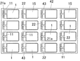
まず始めに、図6Aおよび図6Bに示すように、製造予定の固体電解コンデンサの底壁31を構成する底壁用基板41を準備する。なお発明の理解を容易にするため、本明細書においては、図5の紙面に向かって左側(左方)を「前側(前方)」とし、右側(右方)を「後側(後方)」とし、上下方向を「上下方向」として説明し、図6Aの紙面に向かって上下方向を「左右方向(両側方向)」として説明する。
First, as shown in FIGS. 6A and 6B, a
この底壁用基板41は、前後方向(縦方向)である長手方向(図6Aの左右方向)と、左右方向(横方向)である短手方向(図6Aの上下方向)とにそれぞれ4個ずつ計16個の領域(区画領域:図10の破線で区画した領域)に区分け可能に構成されており、各区画領域が、製造予定の固体電解コンデンサの底壁31を構成可能な底壁構成部位として構成されている。
The
この底壁用基板41の上面(内面)における各底壁構成部位(各区画領域)の前端部に内部陽極回路パターン21aをそれぞれ形成するとともに、各底壁構成部位の前端部を除く領域に内部陰極回路パターン25aをそれぞれ形成する。
An internal
さらに基板41の下面(外面)における各底壁構成部位の前端部に外部陽極回路パターン21bをそれぞれ形成するとともに、各底壁構成部位の後端部に外部陰極回路パターン25bをそれぞれ形成する。
Further, the external
また表裏間において対応し合う内部陽極回路パターン21aと、外部陽極回路パターン21bとは、内周面に導電層が形成されたスルーホール(図示省略)を介してそれぞれ導通させて、互いに電気的に接続する。さらに表裏間において対応し合う内部陰極回路パターン25aと、外部陰極回路パターン25bとは、同様なスルーホール(図示省略)を介して導通させる。
Also, the internal
スルーホールは、例えば、エポキシ樹脂等の樹脂によって、高さが基板41の厚みと同等になるように埋められている。各回路パターン21a,21b,25a,25bとしては、多くの場合、銅が使用され、スルーホールを含めて、回路パターン形成領域にメッキ処理が施されている。メッキとしては、ニッケル下地の錫メッキもしくは金フラッシュメッキが代表例として挙げられる。
The through hole is filled with a resin such as an epoxy resin so that the height is equal to the thickness of the
なお、スルーホールの閉塞部分に施されるメッキと、上記回路パターン21a,21b,25a,25bに施されるメッキとは、導電性の点から金属種を同一に調整するとともに、外観検査の観点から色合いも同様に調整しておくのが好ましい。
The plating applied to the closed portion of the through hole and the plating applied to the
本実施形態において基板41の厚さは1mm以下、好ましくは、0.1〜0.6mmのものが使用される。外部陽極回路パターン21bおよび外部陰極回路パターン25bの寸法は、略同一寸法にしておく。このようにしておくことにより、作製された箱型固体電解コンデンサが回路基板に実装されて使用される場合、従来のモールド封止型の固体電解コンデンサに使用される実装用の基板ランドパターン寸法に適合することができる。従って、本実施形態で製造された固体電解コンデンサを、従来の電子回路基板にそのまま適用することができる。
In this embodiment, the
なお図6Bに示すように、基板41の裏面側(外面側)において、縦方向に隣り合う底壁構成部位のうち、前方側の底壁構成部位に形成された外部陰極回路パターン25bと、後方側の底壁構成部位に形成された外部陽極回路パターン21bとは連続して形成されており、互いに電気的に接続されている。
6B, on the back surface side (outer surface side) of the
また底壁用基板41における各内部陽極回路パターン21aには、枕部材22をそれぞれ取り付ける。
Further, the
本実施形態において、枕部材22は、長さが内部陽極回路パターン21aの左右方向の長さが同寸法のものを使用しているが、それだけに限られず、本発明においては、収容されるコンデンサ素子1の陽極リード11に接続することができれば、枕部材22の長さや形状は特に限定されるものではない。例えば枕部材22として、内部陽極回路パターン21aよりも短いものを使用しても良いし、断面が丸形形状のものであっても、四角形状等の多角形状のものであっても、丸形や多角形を押し潰した扁平な形状のものであっても使用することができる。さらに一つの箱型ケース2内に2個以上の複数のコンデンサ素子1を収容するようなコンデンサを製造する場合、枕部材22としては、複数のコンデンサ素子1の陽極リード11をそれぞれ接続できるような寸法、形状に形成すれば良い。
In the present embodiment, the
枕部材22の材質としては、低抵抗な洋白のような銅合金を使用するのが望ましい。枕部材22と内部陽極回路パターン21aとの接続は、溶接や導電材で行うようにすれば良い。とりわけ、クリーム半田を使用する場合には、抵抗が低く、かつ溶接では困難な面状2次元の接続ができるので、クリーム半田を使用するのが好ましい。クリーム半田を使用する場合には、クリーム半田を内部陽極回路パターン21aの所定場所にディスペンサー等で投与し、枕部材22を載置した後に、枕部材22の上側から加熱してクリーム半田を融解後固化して電気的および機械的に接続するようにすれば良い。
As a material of the
図7Aおよび図7Bに示すように、枕部材22が取り付けられた底壁用基板41に、製造予定の固体電解コンデンサの周側壁32を構成するための周側壁用基板42を取り付ける。
As shown in FIGS. 7A and 7B, a peripheral
周側壁用基板42は、その縦横寸法が基板41の縦横寸法と同一に形成されている。この周側壁用基板42は、底壁用基板41における各底壁構成部位の内部陰陽極回路パターン21a,25aにそれぞれ対応して、略矩形状(略四角形状)の貫通孔43がそれぞれ形成されている。この貫通孔43は、その内周の角部が丸みを帯びていている。
The peripheral
なお後の説明から明らかになるが、周側壁用基板42における各貫通孔43の周縁部が、それぞれ固体電解コンデンサの周側壁32を構成可能な部位として構成されている。
As will become clear from the following description, the peripheral edge portion of each through
この周側壁用基板42は、例えばエポキシ樹脂等の熱硬化性樹脂製のものを使用するのが好ましい。貫通孔43の形成方法としては、熱硬化性樹脂の平板に対し、金型を用いた打ち抜き加工によって、貫通孔43を形成する方法や、ルーターを用いて切削加工することにより、貫通孔43を形成する方法等を好適に採用することができる。
The peripheral
この周側壁用基板42の各貫通孔43を、底壁用基板41の上面における各底壁構成部位の内部陽極回路パターン21aおよび内部陰極回路パターン25aに臨ませるようにして、周側壁用基板42を底壁用基板41上に取り付ける(図8A等参照)。なおこの状態においては、各底壁構成部位の各内部陰陽極回路パターン21a,25aは、各貫通孔43内にそれぞれ配置されている。
Each of the through
周側壁用基板42と底壁用基板41との接続方法は、エポキシ樹脂等の接着剤を使用し加圧加熱して行う方法を採用することができる。
As a method for connecting the peripheral
これにより、上端が開放された凹部を有する箱状のケース本体3に相当する部位が、縦横に4個ずつ連接されたケース本体連続部材が形成される。
As a result, a case body continuous member is formed in which four portions corresponding to the box-shaped
なお、このケース本体連続部材においては、後述するように、貫通孔43である凹部内にコンデンサ素子1がそれぞれ収容されるが、その際に、コンデンサ素子1の上端位置よりも、周側壁用基板42の上端位置が高くなるように寸法設定されている。
In this case body continuous member, as will be described later, each
箱封止による封止方法は、封止時に、樹脂モールド封止に比べコンデンサ素子への応力がかからない。そのため、箱封止は、もろい素材(例えばタングステン)を陽極等に使用したコンデンサ素子の封止にも好ましく適用できる。 The sealing method by box sealing does not apply stress to the capacitor element at the time of sealing as compared with resin mold sealing. Therefore, the box sealing can be preferably applied to the sealing of a capacitor element using a fragile material (for example, tungsten) as an anode.
本実施形態において使用される固体電解コンデンサ素子1は、以下のようにして製造される。
The solid
すなわち、弁作用金属および/または弁作用金属の導電性酸化物の粉に、弁作用金属からなる金属のリード線(陽極リード11)を植立させて成形後焼結し、かつ内部に多数の空隙を有する燒結体を陽極体として、該陽極体上に、弁作用金属の酸化物からなる誘電体層、さらに半導体層、導電体層を順次形成して作製するものである。 That is, a metal lead wire (anode lead 11) made of a valve action metal is planted in the valve action metal and / or a conductive oxide powder of the valve action metal, molded and sintered, and a large number of powders are formed inside. A sintered body having voids is used as an anode body, and a dielectric layer made of an oxide of a valve metal, a semiconductor layer, and a conductor layer are sequentially formed on the anode body.
弁作用金属、弁作用金属の導電性酸化物としては、タンタル、アルミ、チタン、ニオブ、酸化ニオブ、タングステンおよびこれらの合金や組成物を例示することができる。このうち、コンデンサの容量を大きくすることが可能なタングステンおよびタングステンからなる合金や組成物を使用するのが好ましい。本発明において、該合金には、非金属との反応物や固溶体を含み、タングステンの一部が合金化したものを含む。 Examples of the valve action metal and the conductive oxide of the valve action metal include tantalum, aluminum, titanium, niobium, niobium oxide, tungsten, and alloys and compositions thereof. Among these, it is preferable to use an alloy or a composition made of tungsten and tungsten capable of increasing the capacity of the capacitor. In the present invention, the alloy includes a reaction product with a nonmetal or a solid solution, and a part of tungsten alloyed.
陽極リード11としてのリード線は、植立させずに後から燒結体に溶接等で接続させるようにしても良い。陽極リード11としては、タンタルやニオブを好適に用いることができる。
The lead wire as the
また誘電体層は、通常、化成という電解液中で電圧印加する操作で陽極体細孔表面と外表面および陽極リード11の一部に形成される。誘電体層は、陽極体を構成する金属の酸化物からなり、陽極体に存在する他種元素や化成液の電解質の一部が入ることがある。
The dielectric layer is usually formed on the anode body pore surface and outer surface and part of the
焼結体やリード線に用いる弁作用金属等の材料には、コンデンサ特性を損なわない範囲で微量の不純物が含まれていても良い。 A material such as a valve action metal used for the sintered body or the lead wire may contain a small amount of impurities as long as the capacitor characteristics are not impaired.
誘電体層の表層に形成される半導体層は、公知のものが使用される。中でも導電性高分子からなる半導体層は、抵抗が低いので好ましい。陽極体外層に形成された半導体層の陽極リード11の植立面を除いた面上には導電層が形成されて、既述したように陰極部10となる。
As the semiconductor layer formed on the surface of the dielectric layer, a known layer is used. Among these, a semiconductor layer made of a conductive polymer is preferable because of its low resistance. A conductive layer is formed on the surface of the semiconductor layer formed on the outer layer of the anode body excluding the planted surface of the
さらに導電体層として、カーボン層、導電ペースト層、メッキ層の少なくとも1層が形成される。特に、カーボン層と銀ペースト層を順次積層した導電体層が好んで用いられる。 Further, at least one of a carbon layer, a conductive paste layer, and a plating layer is formed as the conductor layer. In particular, a conductor layer in which a carbon layer and a silver paste layer are sequentially laminated is preferably used.
この構成のコンデンサ素子1は、図8Aおよび図8Bに示すように、上記ケース本体連続部材の各凹部(貫通孔43)内にそれぞれ収納される。この場合、コンデンサ素子1の陽極リード11は、長さが長ければ所定寸法に切断した後、枕部材22の上に溶接または導電材によって電気的および機械的に接続する。さらにコンデンサ素子1の陰極部10は、内部陰極回路パターン25aに導電材で電気的および機械的に接続する。
As shown in FIGS. 8A and 8B, the
接着用の導電材としては、導電ペーストや半田を用いることができる。その中でもとりわけ、銀ペーストは、低抵抗であり、かつ使用時に高熱を必要としないので、銀ペーストを使用するのが好ましい。 As the conductive material for bonding, a conductive paste or solder can be used. Among them, silver paste is preferably used because it has low resistance and does not require high heat during use.
なお、ケース本体連続部材の各凹部内に、コンデンサ素子1を複数個収容する場合があるが、その場合は、複数のコンデンサ素子1を方向を揃えて横並びに並列に配置するようにすれば良い。
In some cases, a plurality of
次に図4および図5に示すように、各凹部(貫通孔43)内にコンデンサ素子1が収容されたケース本体連続部材の上端面に、上蓋用基板45を取り付ける。
Next, as shown in FIGS. 4 and 5, the
上蓋用基板45は、その縦横寸法が周側壁用基板42および底壁用基板41の縦横寸法と同一に形成されている。
The vertical and horizontal dimensions of the
上蓋用基板45は、周側壁用基板42の各貫通孔43およびその周縁部に対応する部分が、上蓋35を構成可能な上蓋構成部位として構成されている。
In the
上蓋用基板45の材質としては、エポキシ樹脂等の絶縁性樹脂が用いられる。厚みは、1mm以下、好ましくは0.1〜0.6mmのものが使用される。
As a material of the
また上蓋用基板45の上面における各上蓋構成部位毎に、コンデンサ素子1を識別する記号や番号等を印刷やレーザー加工によってそれぞれ印字しておくようにしても良い。
In addition, a symbol, a number, or the like for identifying the
そして既述したように、この上蓋用基板45によって、周側壁用基板42の上面全域が覆われるようにして、上蓋用基板45を周側壁用基板42の上端面に接着剤を用いて固定する。このとき、周側壁用基板42の上端面に塗布した接着剤によって、上蓋用基板45の各上蓋構成部位の外周縁部を固定する。さらに各コンデンサ素子1の上面である陰極部10の少なくとも一部を、上蓋用基板45の各上蓋構成部位に接着剤5によってそれぞれ固定することにより、コンデンサ素子1と上蓋基板45の上蓋構成部位との各間に接着剤5を充填して、各コンデンサ素子1の上面と上蓋用基板45の各上蓋構成部位とを接着剤5を介して接着固定しておく。
As described above, the
また上蓋用基板45を取り付ける前に、各凹部(各貫通孔43)のコンデンサ素子1の上方の空間内に、絶縁性で低熱伝導性のフィラーを充填しておき、外部からの熱伝達を遅くする手段を講じても良い。低熱伝導性のフィラーとしては、シリカ、ジルコニア等を例示することができる。
Before attaching the
こうして図4および図5に示すように、上蓋用基板45をケース本体連接部品に取り付けることによって、固体電解コンデンサを構成可能な部位(コンデンサ構成部位)が、縦横に4個ずつ接続されたコンデンサ連続部材4が形成される。
As shown in FIGS. 4 and 5, by attaching the
次に、上記コンデンサ連続部材を、各コンデンサ構成部位毎に分割する前に、コンデンサ構成部位が連なったままの状態で、各コンデンサ素子1に対しエージング処理を行うことが好ましい。
Next, it is preferable to perform an aging process on each
このエージング処理を行うに際して、コンデンサ連続部材を用いて図9に示すような電子回路を形成し、縦方向(前後方向)に配置される4個のコンデンサ素子1毎に直列に通電する。すなわち前後方向に隣り合うコンデンサ構成部位において、前側のコンデンサ構成部位の外部陰極回路パターン25bと後側コンデンサ構成部位の外部陽極回路パターン21bとを電気接続して、前後方向(縦方向)に並ぶ複数のコンデンサ素子1を直列に接続しておき、直列に配置される各列の最も上流側(前側)に配置されるコンデンサ素子1の陽極リード11に導通している外部陽極回路パターン21bに、定電流素子61をそれぞれ介して電源から電流を供給するとともに、各列の最も下流側(後側)に配置されるコンデンサ素子1の陰極部10に導通している外部陰極回路パターン25bから共通の導線を通じて上記電源に戻る回路を形成する。
When performing this aging process, an electronic circuit as shown in FIG. 9 is formed using a continuous capacitor member, and the four
定電流素子61としては、適当な電流値のものを使用することで、例えばいずれかのコンデンサ素子1がショート不良をおこし特定のコンデンサ素子1のみに大電流が流れて他のコンデンサ素子1に電流供給が滞ることを防ぐことができ、安定したエージング処理を行うことができる。定電流素子61の一例としては、定電流ダイオード(CRD)を挙げることができる。本実施形態では定電流素子61が電流制限手段を構成するものである。
As the constant
また、特定のコンデンサ素子1のみがショート不良を起こして、その電圧分が他のコンデンサ素子1に必要以上にかかってしまうのを防ぐために、各々のコンデンサ素子1に対し定電圧素子62を並列に配置した電圧制限回路を構成する。これにより、複数のコンデンサ素子1を直列接続してエージング処理できるとともに、処理中にいずれかのコンデンサ素子1に不具合が発生しても、エージング処理を継続することができる。電圧制限回路を構成する定電圧素子の一例としてツェナーダイオードを挙げることができる。本実施形態では、定電圧素子62が電圧制限手段を構成するものである。
In addition, in order to prevent only a
ここで、本実施形態のコンデンサ連続部材4においては、直列方向に隣り合うコンデンサ構成部位において、上流側(図5の左側)に配置されるコンデンサ構成部位の外部陰極回路パターン25bと、下流側(同図の右側)に配置されるコンデンサ構成部位の外部陽極回路パターン21bとは連続して形成されているため、前後方向に並ぶコンデンサ素子1は、当初より直列に電気接続されている。このため、直列方向に並ぶコンデンサ素子1間の配線接続を別途行う必要がなく、その分、エージング処理を簡単に行うことができる。
Here, in the capacitor
エージング処理における通電電圧は、コンデンサ素子1を作製したときの化成電圧以下に設定する。通電時の環境温度は、80〜150℃とし、通電時間は、数週間以内とする。このように通電処理(エージング処理)することにより、内部の固体電解コンデンサ素子1の安定化を図ることができる。
The energization voltage in the aging process is set to be equal to or lower than the formation voltage when the
エージング処理を行った後、コンデンサ連続部材4を、コンデンサ構成部位間の境界線(図10に示した破線)に沿って、基板41,45の表面に対し垂直に切断することによって、コンデンサ構成部位毎に切り出して、図1および図2に示す箱封止型のチップ状固体電解コンデンサを得る。切断の方法は、ルーター式切断、ダイサー式切断およびワイヤーソー工法などから選択することができる。
After performing the aging process, the
なお、作製する固体電解コンデンサは、種類毎に、サイズや形状が規定されているため、コンデンサ連続部材4の切断位置が、周側壁用基板42の隣り合う貫通孔43間における仕切壁の幅方向中央位置となるように、陰陽極回路パターン21a,21b,25a,25bの繰り返しピッチ寸法や、周側壁用基板42の仕切壁の幅寸法を設定しておくと、切断回数を最小限とすることができ、切断作業、ひいてはコンデンサ作製作業を容易に行うことができる。
In addition, since the size and shape of the solid electrolytic capacitor to be produced are regulated for each type, the cutting position of the capacitor
個々に分離された固体電解コンデンサは、必要に応じて、周側壁32の外面、底壁31および上蓋35の外周端面等の切断面を加工処理して、切断による毛羽立ち等の不具合があれば除去する。切断面の加工法としては、ルーター加工やブラスト処理を用いることができる。
Individually separated solid electrolytic capacitors are processed if necessary by cutting the outer surface of the
またブラスト処理を行う場合には、基板裏面の外部陰陽極回路パターン21b,25bのメッキがはげ落ちたり、上蓋35のマーキングが削り落ちてしまったりしないように、マスクや保護板を用意してから行うことが望ましい。さらに上蓋35のマーキングをレーザー加工で行っていた場合は、ブラスト材でのマーキング落ちはわずかであるので、固体電解コンデンサにマスク無しでブラスト処理し、ブラスト処理後に外部陰陽極回路パターン21b,25bに後メッキを行う方法を採用するのが好ましい。これによりマスクを使用する手間を省くことができる。
Also, when performing blasting, prepare a mask or protective plate so that the plating on the external negative and
以上のように、本実施形態の固体電解コンデンサの製造方法によれば、固体電解コンデンサを構成可能な多数のコンデンサ構成部位が連続して設けられたコンデンサ連続部材4を作製した後、そのコンデンサ連続部材4を各コンデンサ構成部位毎に分割して、固体電解コンデンサを得るものであるため、固体電解コンデンサを一度に多数製造することができ、生産効率を向上させることができる。
As described above, according to the method for manufacturing a solid electrolytic capacitor of the present embodiment, after the capacitor
また本実施形態の製法によって得られた箱封止型の固体電解コンデンサによれば、コンデンサ素子1の上面に対し、上蓋35を接着剤5を介して接着固定してるため、上蓋35のほぼ全域が、コンデンサ素子1およびケース本体3に安定状態に支持される。このため、この固体電解コンデンサを電子回路基板に実装した際に、上蓋35に対し高熱が作用したとしても、上蓋35が凹んだり、膨れ上がったりするような不具合を確実に防止することができる。
Further, according to the box-sealed solid electrolytic capacitor obtained by the manufacturing method of the present embodiment, the
さらに本実施形態においては、接着剤5に低熱伝導性のフィラーを充填しておき、熱伝導性を低下させるようにした場合、実装時にコンデンサ素子にかかる熱応力の影響をより一層抑えることができるため、コンデンサ素子1の漏れ電流が極端に増大するようなことがなく、漏れ電流特性の悪化を防止でき、コンデンサとして、より一層高い性能を得ることできる。
Furthermore, in this embodiment, when the adhesive 5 is filled with a low thermal conductivity filler to reduce the thermal conductivity, the influence of thermal stress applied to the capacitor element during mounting can be further suppressed. Therefore, the leakage current of the
なお、上記実施形態においては、箱型ケース2内に、コンデンサ素子1を1個ずつ収容する場合を例に挙げて説明したが、それだけに限られず、本発明において、1つの箱型ケース2内に複数個のコンデンサ素子1を収容するようにしても良い。例えば箱型ケース2(ケース本体3)内に、2個のコンデンサ素子をその陽極リードの引出方向を揃えるように並列配置に収容すれば良い。
In the above-described embodiment, the case where the
また上記実施形態においては、底壁用基板41に周側壁用基板42を接着固定した後、コンデンサ素子1を取り付けるようにしているが、それだけに限られず、本発明においては、底壁用基板41にコンデンサ素子1を取り付けた後、周側壁用基板42を底壁用基板41に対し接着固定するようにしても良い。
In the above embodiment, the
また上記実施形態においては、コンデンサ連続部材を形成するコンデンサ構成部位の数を、縦横に4個ずつ計16個に設定しているが、本発明においては、コンデンサ連続部材を形成するコンデンサ構成部位の数は限定されるものではない。さらに本発明においては、コンデンサ構成部位を、必ずしも、縦横共に複数設ける必要がなく、縦方向および横方向の少なくとも一方のコンデンサ構成部位を1個として、一列構造のコンデンサ連続部材を作製するようにしても良い。 Further, in the above embodiment, the number of capacitor constituent parts forming the capacitor continuous member is set to 16 in total, four vertically and horizontally, but in the present invention, the number of capacitor constituent parts forming the capacitor continuous member is The number is not limited. Furthermore, in the present invention, it is not always necessary to provide a plurality of capacitor components in both the vertical and horizontal directions, and at least one of the capacitor components in the vertical direction and the horizontal direction is used as one to produce a single row capacitor continuous member. Also good.
以下、本発明に関連した実施例について詳細に説明する。 Hereinafter, embodiments related to the present invention will be described in detail.
底板用基板41として、厚さが0.3mm、長さ(縦)寸法が146mm、幅(横)寸法が86mmの銅張りガラスエポキシ基板を準備した。
A copper-clad glass epoxy substrate having a thickness of 0.3 mm, a length (vertical) dimension of 146 mm, and a width (horizontal) dimension of 86 mm was prepared as the
図10Aに示すように、この底板用基板41を、縦方向のピッチT1を7.3mm、横方向のピッチY1を4.3mmで、縦横にそれぞれ20個ずつに分けて、計400の区画領域を得た。なお図10Aにおいては区画領域(底壁構成部位)の各間の境界線を破線で示している。
As shown in FIG. 10A, the
さらに図10Aに示すように、底壁用基板41の表面側(内面側)における各底壁構成部位内に、前端位置から0.5mm(T2参照)離間させ、かつ両端位置からそれぞれ0.4mm(Y2参照)離間させて、縦寸法T3が0.6mm、横寸法(幅寸法)Y3が3.5mmの内部陽極回路パターン21aを形成した。さらにその内部陽極回路パターン21aから後方に1.0mm(T4参照)離間させ、両端位置からそれぞれ0.4mm(Y2参照)離間させて、縦寸法T5が4.7mm、横寸法(幅寸法)Y3が3.5mmの内部陰極回路パターン25aを形成した。なお各底壁構成部位内における内部陽極回路パターン25aの後端位置からの離間寸法T6は0.5mmである。
Further, as shown in FIG. 10A, each bottom wall constituting portion on the front surface side (inner surface side) of the
また図10Bに示すように、底壁用基板41の裏面側(外面側)における各底壁構成部位内に、前端位置から間隔をおかずに、かつ両端位置からそれぞれ0.45mm(Y4参照)離間させて、縦寸法T7が1.3mm、横寸法Y5が3.4mmの外部陽極回路パターン21bを形成した。さらに後端位置から間隔をおかずに、かつ両端位置からそれぞれ0.45mm(Y4参照)離間させて、縦寸法T9が1.3mm、横寸法Y5が3.4mmの外部陰極回路パターン25bを形成した。なお各底壁構成部位内における外部陽極回路パターン21bと外部陰極回路パターン25bとの離間距離T8は4.7mmである。さらに縦方向に隣り合う底壁構成部位のうち、前側(図10Bの左側)に配置される底壁構成部位の外部陰極回路パターン25bと、後側(同図の右側)に配置される底壁構成部位の外部陽極回路パターン21bとは連接されて電気接続されている。
Also, as shown in FIG. 10B, within the bottom wall constituent parts on the back surface side (outer surface side) of the
また各底壁構成部位内において、表裏間で対応し合う陽極回路パターン21a,21b同士と、陰極回路パターン25a,25b同士とはそれぞれスルーホールによって電気的に導通させた。スルーホールは、直径0.5mmであり、孔内がエポキシ樹脂で埋めて、底壁用基板41と同じ厚さに揃えた。
Further, in each bottom wall constituent portion, the
さらにスルーホールの部分を含めて、各回路パターン21a,21b,25a,25bには、ニッケル下地の錫メッキを施した。
Further, each of the
次に、長さ3.0mm、直径0.45mmの洋白線によって構成された枕部材22を、各底壁構成部位内における各内部陽極回路パターン21a上に、同回路パターン21aの横方向(幅方向)に平行に接続した。接続位置は、同回路パターン21aの前端(図10Aの左端)から0.375mmの位置で、各内部陽極回路パターン21aの両側端(図10Aの上下両端)から0.25mmずつを間隔をおいた位置とした。接続方法は、千住金属工業株式会社製のクリーム半田SMX−H05を枕部材22としての洋白線の下に塗布し、その枕部材22の上から加熱して接続した。
Next, a
次いで、周側壁用基板42の材料として、厚さ1.2mmのガラスエポキシ基板を準備した。平面サイズは、長さ(縦寸法)146mm、幅(横寸法)86mmであり、上記の底壁用基板41と同様である。このガラスエポキシ基板に、縦方向(長さ方向)の前後両端から0.5mmの部分をそれぞれ残し、かつ横方向(幅方向)の両端位置から0.4mmの部分をそれぞれ残すようにして、上記の底壁用基板41の各底壁構成部位に対応する部分に、長さ(縦寸法)6.3mm、横(幅寸法)3.5mmの長方形状の貫通孔43を、縦方向に20個、横方向に20個、計400個、等間隔に並べて形成し、周側壁用基板42を作製した。
Next, a glass epoxy substrate having a thickness of 1.2 mm was prepared as a material for the peripheral
この周側壁用基板42において、縦方向に隣り合う貫通孔43,43間の仕切壁の厚みは、1.0mmであり、横方向に隣り合う貫通孔43,43間の仕切壁の厚みは、0.8mmである。
In this
なお、貫通孔43は、別途準備しておいた金型を使用して、周側壁用基板の貫通孔と同形状となるように打ち抜きで形成した。貫通孔43の加工断面の毛羽立ち等の不具合はルーター加工により除去した。
The through
こうして得られた周側壁用基板42の下端面を、パナソニック株式会社製の「プリプレグ1661−HL」からなる繊維状材を介して、上記底壁用基板41の表面側(内面側)に、エポキシ系接着剤を用い、185℃で加圧接合して接着した。これにより、上端が開放された箱部(ケース本体構成部位)が縦横に20個ずつ計400個整列したケース本体連続部材を得た(図8Aおよび図8B参照)。
The lower end surface of the
なおこのケース本体連続部材における各貫通孔43内には、底壁用基板41の表面に形成された内部回路パターン21a,25aがそれぞれ配置されている。
The
上記のケース本体連続部材の作製作業とは別に、コンデンサ素子1を準備した。
A
すなわち、三酸化タングステンを水素還元して得た体積平均粒径0.3μm(0.1〜8μm、比表面積6.3m2/g)のタングステン粉に体積平均粒径0.8μm(0.1〜8μmで5μm以上が7質量%)の市販の珪素粉を0.3質量%混合した粉を、高真空下1280℃で30分放置した。その後、室温に戻し塊状物を解砕して体積平均粒径52μm(180μm未満粉、比表面積2.2m2/g、かさ密度2.6g/cm3、タップ密度5.1g/cm3、CV16万/g)の造粒粉を作製した。この粉と直径0.29mmのタンタル線(陽極リード11)を植立させて成型した後に高真空下1330℃で20分焼結して、大きさが1.0mm×3.0mm×4.45mmの焼結体(粉質量118mg、比表面積1.1m2/g)を2000個作製した。この焼結体においては、1.0mm×3.0mmの面(前面)の中央に、内部に3.7mm埋設し、かつ外部に6.0mm引き出された前記タンタル線(陽極リード11)が植立されている。That is, a tungsten powder having a volume average particle size of 0.3 μm (0.1 to 8 μm, specific surface area of 6.3 m 2 / g) obtained by hydrogen reduction of tungsten trioxide was added to a volume average particle size of 0.8 μm (0.1 μm). A powder obtained by mixing 0.3% by mass of commercially available silicon powder of ˜8 μm and 5 μm or more being 7% by mass) was allowed to stand at 1280 ° C. for 30 minutes under high vacuum. Thereafter, the mass was returned to room temperature, and the mass was crushed to have a volume average particle size of 52 μm (powder less than 180 μm, specific surface area 2.2 m 2 / g, bulk density 2.6 g / cm 3 , tap density 5.1 g / cm 3 , CV16 10,000 / g) of granulated powder was prepared. This powder and a tantalum wire (anode lead 11) having a diameter of 0.29 mm were planted and molded, and then sintered at 1330 ° C. for 20 minutes under high vacuum, and the size was 1.0 mm × 3.0 mm × 4.45 mm. 2000 sintered bodies (powder mass 118 mg, specific surface area 1.1 m 2 / g) were produced. In this sintered body, the tantalum wire (anode lead 11) embedded 3.7 mm inside and drawn 6.0 mm outside is centered on the center (front surface) of 1.0 mm × 3.0 mm. Is standing.
次いで、この焼結体を陽極体として、3質量%の過硫酸カリウム水溶液中で45℃、10V、6時間化成した後に水洗し、次いでエタノール洗浄して速やかに190℃で30分放置後室温に戻して陽極体とリード線の一部に誘電体層を形成した。 Next, the sintered body was used as an anode body, formed in a 3% by mass potassium persulfate aqueous solution at 45 ° C., 10 V, 6 hours, then washed with water, then washed with ethanol, immediately left at 190 ° C. for 30 minutes, and then brought to room temperature. Returning, a dielectric layer was formed on the anode body and part of the lead wire.
さらに誘電体層上にエチレンジオキシチオフェンポリマーにアントラキノンスルホン酸をドープした導電性高分子の半導体層に、カーボン層、銀層を順次積層することにより、タングステン固体電解コンデンサ素子1を640個作製した。なお、焼結体の陽極リード11が植立された1.0mm×3.0mmの面(前面)及び陽極リード11にはカーボン層と銀層は形成していない。
Further, 640 tungsten solid
こうして作製した固体電解コンデンサ素子1から任意の400個を選択し、陽極リード11の先端から4.7mを切断除去した後、前述した400個のケース本体連続部材の各箱部(貫通孔43)内にそれぞれ収納した。このとき、コンデンサ素子1の燒結体寸法で3.0mm×4.45mmの面(下面)で構成される陰極部10を、内部陰極回路パターン25aに載置して、銀ペーストを用いて電気的かつ機械的に接続するとともに、コンデンサ素子1の陽極リード11を、枕部材22としての洋白線に直交するように載置し、抵抗溶接によって電気的かつ機械的に接続した。
Arbitrary 400 pieces are selected from the solid
引き続き、周側壁用基板42の上端面全域と、コンデンサ素子11の上面で構成される陰極部10とにエポキシ系接着剤5を塗布し、周側壁用基板42の上面に、別途用意した厚さ0.3mm、長さ(縦寸法)146mm、横(幅寸法)86mmのガラスエポキシ板からなる上蓋用基板45を接続し、硬化した。
Subsequently, the
これにより、縦横にぞれぞれ20個ずつ計400個の箱封止型の固体電解コンデンサを構成可能なコンデンサ構成部位が連続して設けられたコンデンサ連続部材4(図4および図5参照)を作製した。
Thereby, the capacitor | condenser
次にこのコンデンサ連続部材4における各コンデンサ素子1に対し、上記実施形態と同様にしてエージング処理を行った。
Next, an aging process was performed on each
すなわち、基板裏面の400個の外部陽極回路パターン21bと400個の外部陰極回路パターン25bとに、各々自在に着脱可能な配線冶具を設けた電源回路を接続し、直列配置された各列毎の複数のコンデンサ素子1に対し、電源から7Vの電圧を24時間105℃の環境中でそれぞれ印加し各固体電解コンデンサ素子1を安定化した。なお、電源から各外部陽極回路パターン21bに至る配線中に石塚電子株式会社製「品番E701」の定電流ダイオード(CRD)を配置して電流値を規制した。さらに電圧制御には、株式会社東芝セミコンダクター製のツェナーダイオード「品番DF2S6.8SC」からツェナー電圧が7Vのものを選別して用いた。
That is, a power supply circuit provided with wiring jigs that can be freely attached and detached is connected to 400 external
エージング処理を行った後、コンデンサ連続部材4を、周側壁用基板42の各仕切壁の中間部分を、上蓋用基板45の平面(上面)に対し垂直に切断することによって、個々に分離した箱封止型チップ状固体電解コンデンサを400個得た。この切断処理には、コマツNTC株式会社製「ワイヤーソーMWM442DM」を用いた。
After performing the aging process, the capacitor
こうして作製した固体電解コンデンサは、容量1500μF、定格電圧2.5Vであった。 The solid electrolytic capacitor thus produced had a capacity of 1500 μF and a rated voltage of 2.5V.
本願は、2013年6月6日付で出願された日本国特許出願の特願2013−119555号の優先権主張を伴うものであり、その開示内容は、そのまま本願の一部を構成するものである。 This application is accompanied by the priority claim of Japanese Patent Application No. 2013-119555 of the Japanese patent application filed on June 6, 2013, the disclosure content of which constitutes a part of the present application as it is. .
ここに用いられた用語及び表現は、説明のために用いられたものであって限定的に解釈するために用いられたものではなく、ここに示され且つ述べられた特徴事項の如何なる均等物をも排除するものではなく、この発明のクレームされた範囲内における各種変形をも許容するものであると認識されなければならない。 The terms and expressions used herein are for illustrative purposes and are not to be construed as limiting, but represent any equivalent of the features shown and described herein. It should be recognized that various modifications within the claimed scope of the present invention are permissible.
本発明は、多くの異なった形態で具現化され得るものであるが、この開示は本発明の原理の実施例を提供するものと見なされるべきであって、それら実施例は、本発明をここに記載しかつ/または図示した好ましい実施形態に限定することを意図するものではないという了解のもとで、多くの図示実施形態がここに記載されている。 While this invention may be embodied in many different forms, this disclosure is to be considered as providing examples of the principles of the invention, which examples are hereby incorporated by reference. Many illustrated embodiments are described herein with the understanding that they are not intended to be limited to the preferred embodiments described and / or illustrated.
本発明の図示実施形態を幾つかここに記載したが、本発明は、ここに記載した各種の好ましい実施形態に限定されるものではなく、この開示に基づいていわゆる当業者によって認識され得る、均等な要素、修正、削除、組み合わせ(例えば、各種実施形態に跨る特徴の組み合わせ)、改良及び/又は変更を有するありとあらゆる実施形態をも包含するものである。クレームの限定事項はそのクレームで用いられた用語に基づいて広く解釈されるべきであり、本明細書あるいは本願のプロセキューション中に記載された実施例に限定されるべきではなく、そのような実施例は非排他的であると解釈されるべきである。例えば、この開示において、「preferbly」という用語は非排他的なものであって、「好ましいがこれに限定されるものではない」ということを意味するものである。この開示および本願のプロセキューション中において、ミーンズ・プラス・ファンクションあるいはステップ・プラス・ファンクションの限定事項は、特定クレームの限定事項に関し、a)「means for」あるいは「step for」と明確に記載されており、かつb)それに対応する機能が明確に記載されており、かつc)その構成を裏付ける構成、材料あるいは行為が言及されていない、という条件の全てがその限定事項に存在する場合にのみ適用される。この開示および本願のプロセキューション中において、「present invention」または「invention」という用語は、この開示範囲内における1または複数の側面に言及するものとして使用されている場合がある。このpresent inventionまたはinventionという用語は、臨界を識別するものとして不適切に解釈されるべきではなく、全ての側面すなわち全ての実施形態に亘って適用するものとして不適切に解釈されるべきではなく(すなわち、本発明は多数の側面および実施形態を有していると理解されなければならない)、本願ないしはクレームの範囲を限定するように不適切に解釈されるべきではない。この開示および本願のプロセキューション中において、「embodiment」という用語は、任意の側面、特徴、プロセスあるいはステップ、それらの任意の組み合わせ、及び/又はそれらの任意の部分等を記載する場合にも用いられる。幾つかの実施例においては、各種実施形態は重複する特徴を含む場合がある。この開示および本願のプロセキューション中において、「e.g.,」、「NB」という略字を用いることがあり、それぞれ「たとえば」、「注意せよ」を意味するものである。 Although several illustrated embodiments of the present invention have been described herein, the present invention is not limited to the various preferred embodiments described herein, and is equivalent to what may be recognized by those skilled in the art based on this disclosure. Any and all embodiments having various elements, modifications, deletions, combinations (eg, combinations of features across the various embodiments), improvements and / or changes are encompassed. Claim limitations should be construed broadly based on the terms used in the claims, and should not be limited to the embodiments described herein or in the process of this application, as such The examples should be construed as non-exclusive. For example, in this disclosure, the term “preferably” is non-exclusive and means “preferably but not limited to”. In this disclosure and in the process of this application, means plus function or step plus function limitations are clearly stated as a) “means for” or “step for” with respect to the limitations of the specific claim. And b) the corresponding function is clearly described, and c) all the conditions that the configuration, material or action supporting the configuration are not mentioned are present in the limitation. Applied. In this disclosure and in the process of this application, the term “present invitation” or “invention” may be used to refer to one or more aspects within the scope of this disclosure. This term present invention or invention should not be construed inappropriately as identifying criticality, nor should it be construed as inappropriately applied across all aspects or all embodiments ( That is, it should be understood that the present invention has numerous aspects and embodiments) and should not be construed inappropriately to limit the scope of the present application or the claims. In this disclosure and in the process of this application, the term “embodiment” is also used to describe any aspect, feature, process or step, any combination thereof, and / or any part thereof. It is done. In some examples, various embodiments may include overlapping features. In this disclosure and in the process of the present application, the abbreviations “eg,” and “NB” may be used, meaning “for example” and “note”, respectively.
この発明の固体電解コンデンサの製造方法は、箱封止型の固体電解コンデンサを製造する際に利用可能である。 The method for producing a solid electrolytic capacitor of the present invention can be used when producing a box-sealed solid electrolytic capacitor.
1:コンデンサ素子
10:陰極部
11:陽極リード(陽極部)
2:箱型ケース
21a:内部陽極回路パターン
21b:外部陽極回路パターン
22:枕部材
25a:内部陰極回路パターン
25b:外部陰極回路パターン
31:底壁
32:周側壁
35:上蓋
4:コンデンサ連続部材
41:底壁用基板
42:周壁用部材
43:貫通孔
45:上蓋用基板
5:接着剤
61:定電流素子(電流制御手段)
62:定電圧ダイオード(電圧制御手段)1: Capacitor element 10: Cathode portion 11: Anode lead (anode portion)
2: Box-shaped
62: Constant voltage diode (voltage control means)
Claims (6)
前記底壁を構成可能な底壁構成部位が連続して複数設けられた底壁用基板を準備する工程と、
前記底壁用基板における各底壁構成部位の内面および外面に、内部陰陽極回路パターンおよび外部陰陽極回路パターンをそれぞれ形成するとともに、前記内部陰陽極回路パターンおよび前記外部陰陽極回路パターン間をそれぞれ電気的に接続する工程と、
前記複数の底壁構成部位に対応する配列で複数の貫通孔が設けられた周側壁用基板を準備する工程と、
前記底壁用基板における各底壁構成部位の内部陰陽極回路パターンが前記周側壁用基板の各貫通孔内にそれぞれ配置されるように、前記底壁用基板の内面に前記周側壁用基板を取り付ける工程と、
前記コンデンサ素子として、前端から前方に突出する陽極リードによって陽極部が構成され、かつ少なくとも下面に陰極部が設けられたものを準備する工程と、
前記底壁用基板における各底壁構成部位の内面に前記コンデンサ素子をそれぞれ固定するとともに、各コンデンサ素子の陰陽極部を各底壁構成部位の内部陰陽極回路パターンにそれぞれ電気的に接続する工程と、
前記周側壁用基板における各貫通孔の上端開口部を閉塞するように、前記周側壁用基板上に上蓋用基板を取り付けることにより、前記固体電解コンデンサを構成可能なコンデンサ構成部位が複数連続して設けられたコンデンサ連続部材を得る工程と、
前記コンデンサ連続部材を、各コンデンサ構成部位毎に切断して複数の固体電解コンデンサを得る工程と、
前記コンデンサ連続部材における各コンデンサ素子に対し、エージング処理を行う工程とを含み、
前記エージング処理は、前後方向に隣り合うコンデンサ構成部位において、前側のコンデンサ構成部位の外部陰極回路パターンと後側のコンデンサ構成部位の外部陽極回路パターンとを接続しておき、前後方向に並ぶ複数のコンデンサ構成部位のうち、前端のコンデンサ構成部位の外部陽極回路パターンに電源から電流を供給するとともに、後端のコンデンサ素子の外部陰極回路パターンから電源に電流を戻すことにより、前後方向に並ぶ複数のコンデンサ素子に直列で通電するものとし、
直列に配置される複数のコンデンサ素子に対し、電流制御用の電流制御手段を1つ設けるとともに、各コンデンサ素子毎に、電圧制御用の電圧制御手段をそれぞれ設けるようにしたことを特徴とする固体電解コンデンサの製造方法。 A box-type case in which a peripheral side wall is erected on the outer peripheral edge of the inner surface of the bottom wall, and an upper end opening of the peripheral side wall is closed by an upper lid; and a capacitor element housed in the box-type case A method for producing a solid electrolytic capacitor for producing a box-encapsulated solid electrolytic capacitor,
Preparing a bottom wall substrate in which a plurality of bottom wall components that can form the bottom wall are continuously provided; and
An internal negative electrode circuit pattern and an external negative electrode circuit pattern are respectively formed on the inner surface and the outer surface of each bottom wall constituting part of the bottom wall substrate, and between the internal negative electrode circuit pattern and the external negative electrode circuit pattern, respectively. Electrically connecting, and
Preparing a peripheral side wall substrate provided with a plurality of through holes in an arrangement corresponding to the plurality of bottom wall constituent parts;
The peripheral wall substrate is disposed on the inner surface of the bottom wall substrate so that an internal negative / anodized circuit pattern of each bottom wall constituting portion of the bottom wall substrate is disposed in each through hole of the peripheral wall substrate. Attaching process;
As the capacitor element, preparing an anode part constituted by an anode lead projecting forward from the front end, and having a cathode part provided at least on the lower surface;
The capacitor element is fixed to the inner surface of each bottom wall constituent portion of the bottom wall substrate, and the negative anode portion of each capacitor element is electrically connected to the internal negative anode circuit pattern of each bottom wall constituent portion. When,
By attaching an upper lid substrate on the peripheral side wall substrate so as to close an upper end opening of each through hole in the peripheral side wall substrate, a plurality of capacitor constituent parts capable of configuring the solid electrolytic capacitor are continuously provided. Obtaining the provided capacitor continuous member;
Cutting the capacitor continuous member for each capacitor component to obtain a plurality of solid electrolytic capacitors ;
Aging process for each capacitor element in the capacitor continuous member,
The aging treatment is performed by connecting the external cathode circuit pattern of the front capacitor constituent part and the external anode circuit pattern of the rear capacitor constituent part in the capacitor constituent parts adjacent in the front-rear direction, and arranging a plurality of lines in the front-rear direction. Among the capacitor constituent parts, a current is supplied from the power source to the external anode circuit pattern of the capacitor constituent part at the front end, and a current is returned to the power source from the external cathode circuit pattern of the capacitor element at the rear end, so The capacitor element is energized in series,
A solid state characterized in that one current control means for current control is provided for a plurality of capacitor elements arranged in series, and a voltage control means for voltage control is provided for each capacitor element. Manufacturing method of electrolytic capacitor.
底壁、周側壁および上蓋の外周端面が切断面によって構成されていることを特徴とする固体電解コンデンサ。 A solid electrolytic capacitor manufactured by the manufacturing method according to any one of claims 1 to 5 ,
A solid electrolytic capacitor characterized in that a bottom wall, a peripheral side wall, and an outer peripheral end surface of an upper lid are formed by a cut surface.
Priority Applications (1)
| Application Number | Priority Date | Filing Date | Title |
|---|---|---|---|
| JP2014551440A JP5671663B1 (en) | 2013-06-06 | 2014-06-05 | Solid electrolytic capacitor and manufacturing method thereof |
Applications Claiming Priority (4)
| Application Number | Priority Date | Filing Date | Title |
|---|---|---|---|
| JP2013119555 | 2013-06-06 | ||
| JP2013119555 | 2013-06-06 | ||
| JP2014551440A JP5671663B1 (en) | 2013-06-06 | 2014-06-05 | Solid electrolytic capacitor and manufacturing method thereof |
| PCT/JP2014/064923 WO2014196588A1 (en) | 2013-06-06 | 2014-06-05 | Solid electrolytic capacitor and method for fabricating same |
Publications (2)
| Publication Number | Publication Date |
|---|---|
| JP5671663B1 true JP5671663B1 (en) | 2015-02-18 |
| JPWO2014196588A1 JPWO2014196588A1 (en) | 2017-02-23 |
Family
ID=52008220
Family Applications (1)
| Application Number | Title | Priority Date | Filing Date |
|---|---|---|---|
| JP2014551440A Expired - Fee Related JP5671663B1 (en) | 2013-06-06 | 2014-06-05 | Solid electrolytic capacitor and manufacturing method thereof |
Country Status (4)
| Country | Link |
|---|---|
| US (1) | US9721732B2 (en) |
| JP (1) | JP5671663B1 (en) |
| CN (1) | CN105283935B (en) |
| WO (1) | WO2014196588A1 (en) |
Families Citing this family (6)
| Publication number | Priority date | Publication date | Assignee | Title |
|---|---|---|---|---|
| WO2017048701A1 (en) * | 2015-09-17 | 2017-03-23 | Kemet Electronic Corporation | Methods to reduce case height for capacitors |
| US10163577B2 (en) * | 2016-07-28 | 2018-12-25 | Pacesetter, Inc. | Aluminum electrolytic capacitor and assembly thereof |
| US11087931B2 (en) * | 2018-06-08 | 2021-08-10 | City University Of Hong Kong | Energy storing electrical device and a method of constructing an electrical device |
| CN109545560B (en) * | 2018-10-12 | 2021-05-14 | 福建国光新业科技有限公司 | Method for producing solid electrolytic capacitor |
| CN110010377B (en) * | 2019-04-12 | 2020-11-27 | 西安太乙电子有限公司 | Surface-mounted ceramic dielectric capacitor installation aging device and method |
| TWI836337B (en) * | 2021-02-09 | 2024-03-21 | 智威科技股份有限公司 | Electronic component packaging structure, manufacturing method thereof and semi-finished product assembly |
Citations (7)
| Publication number | Priority date | Publication date | Assignee | Title |
|---|---|---|---|---|
| JP2000003832A (en) * | 1998-06-16 | 2000-01-07 | Hitachi Aic Inc | Manufacture of solid electrolytic capacitor |
| JP2001052961A (en) * | 1999-06-01 | 2001-02-23 | Rohm Co Ltd | Structure of packaged solid electrolytic capacitor and manufacture thereof |
| JP2004349658A (en) * | 2002-07-26 | 2004-12-09 | Sanyo Electric Co Ltd | Electrolytic capacitor |
| JP2006014589A (en) * | 2004-06-21 | 2006-01-12 | Inventio Ag | Circuit structure for limiting overvoltage in energy storage module |
| JP2006278875A (en) * | 2005-03-30 | 2006-10-12 | Sanyo Electric Co Ltd | Solid electrolytic capacitor |
| JP2011071177A (en) * | 2009-09-24 | 2011-04-07 | Holy Stone Polytech Co Ltd | Aging method of solid electrolytic capacitor |
| JP2012222344A (en) * | 2011-04-07 | 2012-11-12 | Avx Corp | Multi-anode solid electrolytic capacitor assembly |
Family Cites Families (3)
| Publication number | Priority date | Publication date | Assignee | Title |
|---|---|---|---|---|
| JP2921416B2 (en) | 1994-11-25 | 1999-07-19 | 日本電気株式会社 | Solid electrolytic capacitor and method of manufacturing the same |
| TWI225656B (en) * | 2002-07-26 | 2004-12-21 | Sanyo Electric Co | Electrolytic capacitor and a fabrication method therefor |
| JP4879845B2 (en) | 2007-08-24 | 2012-02-22 | Necトーキン株式会社 | Surface mount capacitor and method of manufacturing the same |
-
2014
- 2014-06-05 JP JP2014551440A patent/JP5671663B1/en not_active Expired - Fee Related
- 2014-06-05 US US14/780,095 patent/US9721732B2/en not_active Expired - Fee Related
- 2014-06-05 CN CN201480006731.5A patent/CN105283935B/en not_active Expired - Fee Related
- 2014-06-05 WO PCT/JP2014/064923 patent/WO2014196588A1/en not_active Ceased
Patent Citations (7)
| Publication number | Priority date | Publication date | Assignee | Title |
|---|---|---|---|---|
| JP2000003832A (en) * | 1998-06-16 | 2000-01-07 | Hitachi Aic Inc | Manufacture of solid electrolytic capacitor |
| JP2001052961A (en) * | 1999-06-01 | 2001-02-23 | Rohm Co Ltd | Structure of packaged solid electrolytic capacitor and manufacture thereof |
| JP2004349658A (en) * | 2002-07-26 | 2004-12-09 | Sanyo Electric Co Ltd | Electrolytic capacitor |
| JP2006014589A (en) * | 2004-06-21 | 2006-01-12 | Inventio Ag | Circuit structure for limiting overvoltage in energy storage module |
| JP2006278875A (en) * | 2005-03-30 | 2006-10-12 | Sanyo Electric Co Ltd | Solid electrolytic capacitor |
| JP2011071177A (en) * | 2009-09-24 | 2011-04-07 | Holy Stone Polytech Co Ltd | Aging method of solid electrolytic capacitor |
| JP2012222344A (en) * | 2011-04-07 | 2012-11-12 | Avx Corp | Multi-anode solid electrolytic capacitor assembly |
Also Published As
| Publication number | Publication date |
|---|---|
| WO2014196588A1 (en) | 2014-12-11 |
| US9721732B2 (en) | 2017-08-01 |
| US20160049259A1 (en) | 2016-02-18 |
| CN105283935A (en) | 2016-01-27 |
| JPWO2014196588A1 (en) | 2017-02-23 |
| CN105283935B (en) | 2018-06-08 |
Similar Documents
| Publication | Publication Date | Title |
|---|---|---|
| JP5671663B1 (en) | Solid electrolytic capacitor and manufacturing method thereof | |
| JP5152946B2 (en) | Solid electrolytic capacitor and manufacturing method thereof | |
| TWI271761B (en) | Solid electrolytic capacitor and its manufacturing method | |
| JP5007677B2 (en) | Solid electrolytic capacitor and manufacturing method thereof | |
| KR102138890B1 (en) | Tantalum capacitor and method of preparing the same | |
| JP5671664B1 (en) | Solid electrolytic capacitor, anode lead connection method thereof, and manufacturing method of solid electrolytic capacitor | |
| JP5201671B2 (en) | Bottom electrode type solid electrolytic capacitor and manufacturing method thereof | |
| JP2006190965A (en) | Solid electrolytic capacitor with bottom-surface terminals, manufacturing method therefor, and lead frame for use therein | |
| JP4653682B2 (en) | Chip-shaped solid electrolytic capacitor | |
| JP2017092237A (en) | Solid electrolytic capacitor and manufacturing method thereof | |
| KR102052763B1 (en) | Tantalum capacitor and method of preparing the same | |
| JP5376134B2 (en) | Solid electrolytic capacitor | |
| JP2005158903A (en) | Solid electrolytic capacitor | |
| JP2009054681A (en) | Surface-mounted capacitor, and manufacturing method thereof | |
| JP2009182276A (en) | Solid-state electrolytic capacitor and method of manufacturing the same | |
| JP5035999B2 (en) | Solid electrolytic capacitor and manufacturing method thereof | |
| JP2007142161A (en) | Underside-electrode solid electrolytic capacitor | |
| JP2011176067A (en) | Solid-state electrolytic capacitor | |
| JP2009295645A (en) | Solid electrolytic capacitor | |
| JP2005101480A (en) | Electronic component equipped with lead frame | |
| JP5326032B1 (en) | Solid electrolytic capacitor | |
| JP5376135B2 (en) | Manufacturing method of solid electrolytic capacitor | |
| JP5258071B2 (en) | Solid electrolytic capacitor | |
| US9251954B2 (en) | Jig for manufacturing capacitor element and method for manufacturing capacitor element | |
| JP2008109007A (en) | Method of manufacturing bottom-surface electrode type solid-state electrolytic capacitor, and lead frame used for the same |
Legal Events
| Date | Code | Title | Description |
|---|---|---|---|
| TRDD | Decision of grant or rejection written | ||
| A975 | Report on accelerated examination |
Free format text: JAPANESE INTERMEDIATE CODE: A971005 Effective date: 20141128 |
|
| A01 | Written decision to grant a patent or to grant a registration (utility model) |
Free format text: JAPANESE INTERMEDIATE CODE: A01 Effective date: 20141202 |
|
| A61 | First payment of annual fees (during grant procedure) |
Free format text: JAPANESE INTERMEDIATE CODE: A61 Effective date: 20141219 |
|
| R150 | Certificate of patent or registration of utility model |
Ref document number: 5671663 Country of ref document: JP Free format text: JAPANESE INTERMEDIATE CODE: R150 |
|
| RD02 | Notification of acceptance of power of attorney |
Free format text: JAPANESE INTERMEDIATE CODE: R3D02 |
|
| S111 | Request for change of ownership or part of ownership |
Free format text: JAPANESE INTERMEDIATE CODE: R313111 |
|
| R350 | Written notification of registration of transfer |
Free format text: JAPANESE INTERMEDIATE CODE: R350 |
|
| S531 | Written request for registration of change of domicile |
Free format text: JAPANESE INTERMEDIATE CODE: R313531 |
|
| R350 | Written notification of registration of transfer |
Free format text: JAPANESE INTERMEDIATE CODE: R350 |
|
| LAPS | Cancellation because of no payment of annual fees |