JP5657775B2 - 薄いパッドにおける窓のモールディング - Google Patents
薄いパッドにおける窓のモールディング Download PDFInfo
- Publication number
- JP5657775B2 JP5657775B2 JP2013504907A JP2013504907A JP5657775B2 JP 5657775 B2 JP5657775 B2 JP 5657775B2 JP 2013504907 A JP2013504907 A JP 2013504907A JP 2013504907 A JP2013504907 A JP 2013504907A JP 5657775 B2 JP5657775 B2 JP 5657775B2
- Authority
- JP
- Japan
- Prior art keywords
- polishing
- layer
- window
- recess
- polishing layer
- Prior art date
- Legal status (The legal status is an assumption and is not a legal conclusion. Google has not performed a legal analysis and makes no representation as to the accuracy of the status listed.)
- Active
Links
- 238000000465 moulding Methods 0.000 title description 2
- 238000005498 polishing Methods 0.000 claims description 146
- 239000010410 layer Substances 0.000 claims description 73
- 239000012790 adhesive layer Substances 0.000 claims description 38
- 238000000034 method Methods 0.000 claims description 24
- 229920000642 polymer Polymers 0.000 claims description 20
- 239000007788 liquid Substances 0.000 claims description 14
- 238000004519 manufacturing process Methods 0.000 claims description 6
- 229910052751 metal Inorganic materials 0.000 claims description 6
- 239000002184 metal Substances 0.000 claims description 6
- 238000003825 pressing Methods 0.000 claims description 6
- 238000010438 heat treatment Methods 0.000 claims description 5
- 238000007789 sealing Methods 0.000 claims description 5
- 239000002356 single layer Substances 0.000 claims description 5
- 230000000149 penetrating effect Effects 0.000 claims 1
- 239000000758 substrate Substances 0.000 description 32
- 239000010408 film Substances 0.000 description 10
- 238000012544 monitoring process Methods 0.000 description 8
- 238000001228 spectrum Methods 0.000 description 8
- 230000003287 optical effect Effects 0.000 description 7
- KWYUFKZDYYNOTN-UHFFFAOYSA-M Potassium hydroxide Chemical compound [OH-].[K+] KWYUFKZDYYNOTN-UHFFFAOYSA-M 0.000 description 6
- 239000000463 material Substances 0.000 description 6
- 239000007787 solid Substances 0.000 description 6
- XEEYBQQBJWHFJM-UHFFFAOYSA-N Iron Chemical compound [Fe] XEEYBQQBJWHFJM-UHFFFAOYSA-N 0.000 description 4
- 239000002390 adhesive tape Substances 0.000 description 4
- -1 polyethylene terephthalate Polymers 0.000 description 4
- 229920000139 polyethylene terephthalate Polymers 0.000 description 4
- 239000005020 polyethylene terephthalate Substances 0.000 description 4
- 229920001343 polytetrafluoroethylene Polymers 0.000 description 4
- 239000004810 polytetrafluoroethylene Substances 0.000 description 4
- 230000008569 process Effects 0.000 description 4
- 239000002002 slurry Substances 0.000 description 4
- 239000000126 substance Substances 0.000 description 4
- 239000004820 Pressure-sensitive adhesive Substances 0.000 description 3
- 239000013307 optical fiber Substances 0.000 description 3
- 239000011148 porous material Substances 0.000 description 3
- 239000004065 semiconductor Substances 0.000 description 3
- 229920002799 BoPET Polymers 0.000 description 2
- LFQSCWFLJHTTHZ-UHFFFAOYSA-N Ethanol Chemical compound CCO LFQSCWFLJHTTHZ-UHFFFAOYSA-N 0.000 description 2
- VYPSYNLAJGMNEJ-UHFFFAOYSA-N Silicium dioxide Chemical compound O=[Si]=O VYPSYNLAJGMNEJ-UHFFFAOYSA-N 0.000 description 2
- 239000004809 Teflon Substances 0.000 description 2
- 229920006362 Teflon® Polymers 0.000 description 2
- 239000000853 adhesive Substances 0.000 description 2
- 230000001070 adhesive effect Effects 0.000 description 2
- 230000005540 biological transmission Effects 0.000 description 2
- 238000004049 embossing Methods 0.000 description 2
- 229910052742 iron Inorganic materials 0.000 description 2
- 239000000203 mixture Substances 0.000 description 2
- 239000002245 particle Substances 0.000 description 2
- 238000007517 polishing process Methods 0.000 description 2
- 229920002635 polyurethane Polymers 0.000 description 2
- 239000004814 polyurethane Substances 0.000 description 2
- 239000005041 Mylar™ Substances 0.000 description 1
- 229910000831 Steel Inorganic materials 0.000 description 1
- 239000006061 abrasive grain Substances 0.000 description 1
- 229910052782 aluminium Inorganic materials 0.000 description 1
- XAGFODPZIPBFFR-UHFFFAOYSA-N aluminium Chemical compound [Al] XAGFODPZIPBFFR-UHFFFAOYSA-N 0.000 description 1
- 230000008859 change Effects 0.000 description 1
- 238000004891 communication Methods 0.000 description 1
- 230000006835 compression Effects 0.000 description 1
- 238000007906 compression Methods 0.000 description 1
- 239000004020 conductor Substances 0.000 description 1
- 230000032798 delamination Effects 0.000 description 1
- 238000001514 detection method Methods 0.000 description 1
- 239000010432 diamond Substances 0.000 description 1
- 229910003460 diamond Inorganic materials 0.000 description 1
- 238000005553 drilling Methods 0.000 description 1
- 239000000835 fiber Substances 0.000 description 1
- 239000012530 fluid Substances 0.000 description 1
- 229910021485 fumed silica Inorganic materials 0.000 description 1
- 238000012625 in-situ measurement Methods 0.000 description 1
- 238000011065 in-situ storage Methods 0.000 description 1
- 238000009434 installation Methods 0.000 description 1
- 230000001788 irregular Effects 0.000 description 1
- 238000012886 linear function Methods 0.000 description 1
- 238000012986 modification Methods 0.000 description 1
- 230000004048 modification Effects 0.000 description 1
- 238000000206 photolithography Methods 0.000 description 1
- 239000004033 plastic Substances 0.000 description 1
- 229920003023 plastic Polymers 0.000 description 1
- 229920002959 polymer blend Polymers 0.000 description 1
- 239000010453 quartz Substances 0.000 description 1
- 238000002310 reflectometry Methods 0.000 description 1
- 238000005476 soldering Methods 0.000 description 1
- 239000010959 steel Substances 0.000 description 1
- 238000012360 testing method Methods 0.000 description 1
- 239000010409 thin film Substances 0.000 description 1
- 238000013519 translation Methods 0.000 description 1
- 235000012773 waffles Nutrition 0.000 description 1
Images


Classifications
-
- B—PERFORMING OPERATIONS; TRANSPORTING
- B24—GRINDING; POLISHING
- B24B—MACHINES, DEVICES, OR PROCESSES FOR GRINDING OR POLISHING; DRESSING OR CONDITIONING OF ABRADING SURFACES; FEEDING OF GRINDING, POLISHING, OR LAPPING AGENTS
- B24B37/00—Lapping machines or devices; Accessories
- B24B37/11—Lapping tools
- B24B37/20—Lapping pads for working plane surfaces
- B24B37/205—Lapping pads for working plane surfaces provided with a window for inspecting the surface of the work being lapped
-
- H—ELECTRICITY
- H01—ELECTRIC ELEMENTS
- H01L—SEMICONDUCTOR DEVICES NOT COVERED BY CLASS H10
- H01L21/00—Processes or apparatus adapted for the manufacture or treatment of semiconductor or solid state devices or of parts thereof
- H01L21/02—Manufacture or treatment of semiconductor devices or of parts thereof
- H01L21/04—Manufacture or treatment of semiconductor devices or of parts thereof the devices having potential barriers, e.g. a PN junction, depletion layer or carrier concentration layer
- H01L21/18—Manufacture or treatment of semiconductor devices or of parts thereof the devices having potential barriers, e.g. a PN junction, depletion layer or carrier concentration layer the devices having semiconductor bodies comprising elements of Group IV of the Periodic Table or AIIIBV compounds with or without impurities, e.g. doping materials
- H01L21/30—Treatment of semiconductor bodies using processes or apparatus not provided for in groups H01L21/20 - H01L21/26
- H01L21/302—Treatment of semiconductor bodies using processes or apparatus not provided for in groups H01L21/20 - H01L21/26 to change their surface-physical characteristics or shape, e.g. etching, polishing, cutting
- H01L21/304—Mechanical treatment, e.g. grinding, polishing, cutting
-
- B—PERFORMING OPERATIONS; TRANSPORTING
- B24—GRINDING; POLISHING
- B24B—MACHINES, DEVICES, OR PROCESSES FOR GRINDING OR POLISHING; DRESSING OR CONDITIONING OF ABRADING SURFACES; FEEDING OF GRINDING, POLISHING, OR LAPPING AGENTS
- B24B37/00—Lapping machines or devices; Accessories
- B24B37/11—Lapping tools
-
- B—PERFORMING OPERATIONS; TRANSPORTING
- B24—GRINDING; POLISHING
- B24D—TOOLS FOR GRINDING, BUFFING OR SHARPENING
- B24D11/00—Constructional features of flexible abrasive materials; Special features in the manufacture of such materials
-
- H—ELECTRICITY
- H01—ELECTRIC ELEMENTS
- H01L—SEMICONDUCTOR DEVICES NOT COVERED BY CLASS H10
- H01L21/00—Processes or apparatus adapted for the manufacture or treatment of semiconductor or solid state devices or of parts thereof
- H01L21/67—Apparatus specially adapted for handling semiconductor or electric solid state devices during manufacture or treatment thereof; Apparatus specially adapted for handling wafers during manufacture or treatment of semiconductor or electric solid state devices or components ; Apparatus not specifically provided for elsewhere
- H01L21/67005—Apparatus not specifically provided for elsewhere
- H01L21/67011—Apparatus for manufacture or treatment
- H01L21/67092—Apparatus for mechanical treatment
Landscapes
- Engineering & Computer Science (AREA)
- Mechanical Engineering (AREA)
- Physics & Mathematics (AREA)
- Condensed Matter Physics & Semiconductors (AREA)
- General Physics & Mathematics (AREA)
- Manufacturing & Machinery (AREA)
- Computer Hardware Design (AREA)
- Microelectronics & Electronic Packaging (AREA)
- Power Engineering (AREA)
- Mechanical Treatment Of Semiconductor (AREA)
- Finish Polishing, Edge Sharpening, And Grinding By Specific Grinding Devices (AREA)
Description
Claims (13)
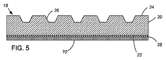
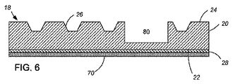
- 研磨パッドを作製する方法であって、
研磨層の一領域を圧縮し且つ研磨層に凹みを形成するために、前記領域の表面を押圧し且つ加熱するステップであって、前記凹みは、前記研磨層に垂直な方向に部分的に延びるが前記研磨層を完全には貫かず、前記凹みは、第1の横方向の寸法を有する、ステップと、
前記研磨層および接着層を貫通する孔を形成するステップであって、前記孔が、前記凹み内に配置されていて、前記凹みの第1の横方向の寸法より小さい第2の横方向の寸法を有し、前記凹みと孔との組み合わせによって前記研磨層および接着層を貫く開孔が提供されるステップと、
前記孔に広がるように前記研磨層の表面の反対側でシールフィルムを前記接着層に固着するステップと、
液体ポリマーを前記開孔の中に分配するステップと、
前記液体ポリマーを硬化して窓を形成するステップと
を含む方法。 - 前記凹みを形成する前に前記接着層をライナで覆い、前記ライナを剥がして前記接着層に前記シールフィルムを固着し、前記液体ポリマーが硬化した後に前記ライナで前記接着層を再度覆うステップをさらに含む、請求項1に記載の方法。
- 前記表面の上に突き出ている硬化ポリマーの一部分を除去するステップをさらに含む、請求項1に記載の方法。
- 前記研磨層は単一の層から成る、請求項1に記載の方法。
- 前記研磨層の表面を押圧し且つ加熱するステップは前記研磨層を加熱金属片で押し付けるステップを含む、請求項1に記載の方法。
- 前記孔を形成するステップは、前記研磨層の前記研磨表面側から前記研磨層および前記接着層に貫通孔を開けるステップを含む、請求項1に記載の方法。
- 前記窓は、前記凹みにある上部と前記孔にある下部とを含み、前記上部は前記窓の全側面上で前記下部を越えて横方向に突き出ている、請求項1に記載の方法。
- 前記上部の横方向の寸法は前記下部の横方向の寸法の2倍〜4倍大きい、請求項7に記載の方法。
- 前記研磨パッドの全体の厚さは1mm未満である、請求項1に記載の方法。
- 前記下部が前記上部の中心に配置される、請求項7に記載の方法。
- 前記窓は円形であり、前記上部と下部とは同心である、請求項10に記載の方法。
- 前記上部の直径は約6mmであり、前記下部の直径は約3mmである、請求項11に記載の方法。
- 前記研磨層の表面内に溝を形成するステップをさらに含む、請求項1に記載の方法。
Applications Claiming Priority (3)
| Application Number | Priority Date | Filing Date | Title |
|---|---|---|---|
| US12/762,175 | 2010-04-16 | ||
| US12/762,175 US8393940B2 (en) | 2010-04-16 | 2010-04-16 | Molding windows in thin pads |
| PCT/US2011/029468 WO2011129959A2 (en) | 2010-04-16 | 2011-03-22 | Molding windows in thin pads |
Publications (3)
| Publication Number | Publication Date |
|---|---|
| JP2013525124A JP2013525124A (ja) | 2013-06-20 |
| JP2013525124A5 JP2013525124A5 (ja) | 2014-05-08 |
| JP5657775B2 true JP5657775B2 (ja) | 2015-01-21 |
Family
ID=44788545
Family Applications (1)
| Application Number | Title | Priority Date | Filing Date |
|---|---|---|---|
| JP2013504907A Active JP5657775B2 (ja) | 2010-04-16 | 2011-03-22 | 薄いパッドにおける窓のモールディング |
Country Status (5)
| Country | Link |
|---|---|
| US (1) | US8393940B2 (ja) |
| JP (1) | JP5657775B2 (ja) |
| KR (1) | KR101761389B1 (ja) |
| TW (1) | TWI461255B (ja) |
| WO (1) | WO2011129959A2 (ja) |
Families Citing this family (20)
| Publication number | Priority date | Publication date | Assignee | Title |
|---|---|---|---|---|
| US8562389B2 (en) * | 2007-06-08 | 2013-10-22 | Applied Materials, Inc. | Thin polishing pad with window and molding process |
| WO2012068428A2 (en) * | 2010-11-18 | 2012-05-24 | Cabot Microelectronics Corporation | Polishing pad comprising transmissive region |
| US8535115B2 (en) * | 2011-01-28 | 2013-09-17 | Applied Materials, Inc. | Gathering spectra from multiple optical heads |
| JP5893479B2 (ja) * | 2011-04-21 | 2016-03-23 | 東洋ゴム工業株式会社 | 積層研磨パッド |
| US9597769B2 (en) * | 2012-06-04 | 2017-03-21 | Nexplanar Corporation | Polishing pad with polishing surface layer having an aperture or opening above a transparent foundation layer |
| ITTV20120147A1 (it) * | 2012-07-30 | 2014-01-31 | Hausbrandt Trieste 1892 Spa | Capsula per la preparazione di bevande |
| US8961266B2 (en) * | 2013-03-15 | 2015-02-24 | Applied Materials, Inc. | Polishing pad with secondary window seal |
| KR20160147917A (ko) * | 2014-05-02 | 2016-12-23 | 쓰리엠 이노베이티브 프로퍼티즈 컴파니 | 불연속된 구조화된 연마 용품 및 작업편의 연마 방법 |
| US9868185B2 (en) * | 2015-11-03 | 2018-01-16 | Cabot Microelectronics Corporation | Polishing pad with foundation layer and window attached thereto |
| US10213894B2 (en) | 2016-02-26 | 2019-02-26 | Applied Materials, Inc. | Method of placing window in thin polishing pad |
| WO2018005767A1 (en) * | 2016-06-29 | 2018-01-04 | Saint-Gobain Abrasives, Inc. | Abrasive tools and methods for forming same |
| TWI629297B (zh) * | 2016-07-05 | 2018-07-11 | 智勝科技股份有限公司 | 研磨層及其製造方法以及研磨方法 |
| US10259099B2 (en) * | 2016-08-04 | 2019-04-16 | Rohm And Haas Electronic Materials Cmp Holdings, Inc. | Tapering method for poromeric polishing pad |
| CN109641342A (zh) * | 2016-08-31 | 2019-04-16 | 应用材料公司 | 具有环形工作台或抛光垫的抛光系统 |
| KR101947877B1 (ko) * | 2016-11-24 | 2019-02-13 | 두산중공업 주식회사 | 병렬 복열 방식의 초임계 이산화탄소 발전 시스템 |
| KR101904322B1 (ko) * | 2017-01-23 | 2018-10-04 | 에스케이씨 주식회사 | 연마패드 및 이의 제조방법 |
| TWI650202B (zh) * | 2017-08-22 | 2019-02-11 | 智勝科技股份有限公司 | 研磨墊、研磨墊的製造方法及研磨方法 |
| US10569383B2 (en) | 2017-09-15 | 2020-02-25 | Rohm And Haas Electronic Materials Cmp Holdings, Inc. | Flanged optical endpoint detection windows and CMP polishing pads containing them |
| US11325221B2 (en) * | 2017-11-16 | 2022-05-10 | Rohm And Haas Electronic Materials Cmp Holdings, Inc. | Polishing pad with multipurpose composite window |
| JP7134005B2 (ja) * | 2018-07-26 | 2022-09-09 | 富士紡ホールディングス株式会社 | 研磨パッド |
Family Cites Families (18)
| Publication number | Priority date | Publication date | Assignee | Title |
|---|---|---|---|---|
| JPH08197434A (ja) * | 1995-01-23 | 1996-08-06 | Sony Corp | 研磨用パッド |
| JP3431115B2 (ja) * | 1995-03-28 | 2003-07-28 | アプライド マテリアルズ インコーポレイテッド | ケミカルメカニカルポリシングの操作をインシチュウでモニタするための装置及び方法 |
| US5893796A (en) * | 1995-03-28 | 1999-04-13 | Applied Materials, Inc. | Forming a transparent window in a polishing pad for a chemical mechanical polishing apparatus |
| US5738574A (en) | 1995-10-27 | 1998-04-14 | Applied Materials, Inc. | Continuous processing system for chemical mechanical polishing |
| US6994607B2 (en) * | 2001-12-28 | 2006-02-07 | Applied Materials, Inc. | Polishing pad with window |
| JP2003510826A (ja) * | 1999-09-29 | 2003-03-18 | ロデール ホールディングス インコーポレイテッド | 研磨パッド |
| US6685537B1 (en) | 2000-06-05 | 2004-02-03 | Speedfam-Ipec Corporation | Polishing pad window for a chemical mechanical polishing tool |
| KR100858392B1 (ko) | 2001-04-25 | 2008-09-11 | 제이에스알 가부시끼가이샤 | 반도체 웨이퍼용 연마 패드와, 이를 구비한 반도체웨이퍼용 연마 적층체와, 반도체 웨이퍼의 연마 방법 |
| JP2003273046A (ja) * | 2002-03-13 | 2003-09-26 | Nihon Micro Coating Co Ltd | 研磨装置及びテープ並びに方法 |
| US6875077B2 (en) * | 2002-03-18 | 2005-04-05 | Raytech Innovative Solutions, Inc. | Polishing pad for use in chemical/mechanical planarization of semiconductor wafers having a transparent window for end-point determination and method of making |
| JP2008044103A (ja) * | 2003-04-09 | 2008-02-28 | Jsr Corp | 研磨複層体および半導体ウエハの研磨方法 |
| JP2004343090A (ja) * | 2003-04-22 | 2004-12-02 | Jsr Corp | 研磨パッドおよび半導体ウェハの研磨方法 |
| KR20040093402A (ko) * | 2003-04-22 | 2004-11-05 | 제이에스알 가부시끼가이샤 | 연마 패드 및 반도체 웨이퍼의 연마 방법 |
| US6986705B2 (en) * | 2004-04-05 | 2006-01-17 | Rimpad Tech Ltd. | Polishing pad and method of making same |
| WO2005104199A1 (ja) * | 2004-04-23 | 2005-11-03 | Jsr Corporation | 半導体ウエハ用研磨パッド及びこれを備える半導体ウエハ用研磨複層体並びに半導体ウエハの研磨方法 |
| JP4904027B2 (ja) | 2005-08-10 | 2012-03-28 | ニッタ・ハース株式会社 | 研磨パッド |
| US7179151B1 (en) * | 2006-03-27 | 2007-02-20 | Freescale Semiconductor, Inc. | Polishing pad, a polishing apparatus, and a process for using the polishing pad |
| US8562389B2 (en) | 2007-06-08 | 2013-10-22 | Applied Materials, Inc. | Thin polishing pad with window and molding process |
-
2010
- 2010-04-16 US US12/762,175 patent/US8393940B2/en active Active
-
2011
- 2011-03-22 JP JP2013504907A patent/JP5657775B2/ja active Active
- 2011-03-22 KR KR1020127030038A patent/KR101761389B1/ko active IP Right Grant
- 2011-03-22 WO PCT/US2011/029468 patent/WO2011129959A2/en active Application Filing
- 2011-03-25 TW TW100110367A patent/TWI461255B/zh active
Also Published As
| Publication number | Publication date |
|---|---|
| WO2011129959A2 (en) | 2011-10-20 |
| KR101761389B1 (ko) | 2017-07-25 |
| TWI461255B (zh) | 2014-11-21 |
| JP2013525124A (ja) | 2013-06-20 |
| WO2011129959A3 (en) | 2012-04-19 |
| US20110256818A1 (en) | 2011-10-20 |
| TW201143969A (en) | 2011-12-16 |
| KR20130088744A (ko) | 2013-08-08 |
| US8393940B2 (en) | 2013-03-12 |
Similar Documents
| Publication | Publication Date | Title |
|---|---|---|
| JP5657775B2 (ja) | 薄いパッドにおける窓のモールディング | |
| JP5363470B2 (ja) | 窓付きの薄い研磨パッド及び成形プロセス | |
| KR101956848B1 (ko) | 폴리싱 패드 조립체 | |
| JP5277163B2 (ja) | 複数の部分を有する窓をもつ研磨パッド | |
| TWI780978B (zh) | 拋光墊及其製造方法 | |
| TWI587977B (zh) | 帶有次窗密封件的拋光墊及形成此拋光墊的方法 | |
| JP6794464B2 (ja) | 薄い研磨パッド内の窓 | |
| TW202417180A (zh) | 拋光墊及其製造方法 |
Legal Events
| Date | Code | Title | Description |
|---|---|---|---|
| A521 | Request for written amendment filed |
Free format text: JAPANESE INTERMEDIATE CODE: A523 Effective date: 20140320 |
|
| A621 | Written request for application examination |
Free format text: JAPANESE INTERMEDIATE CODE: A621 Effective date: 20140320 |
|
| A871 | Explanation of circumstances concerning accelerated examination |
Free format text: JAPANESE INTERMEDIATE CODE: A871 Effective date: 20140320 |
|
| A975 | Report on accelerated examination |
Free format text: JAPANESE INTERMEDIATE CODE: A971005 Effective date: 20140421 |
|
| A131 | Notification of reasons for refusal |
Free format text: JAPANESE INTERMEDIATE CODE: A131 Effective date: 20140430 |
|
| A601 | Written request for extension of time |
Free format text: JAPANESE INTERMEDIATE CODE: A601 Effective date: 20140725 |
|
| A602 | Written permission of extension of time |
Free format text: JAPANESE INTERMEDIATE CODE: A602 Effective date: 20140801 |
|
| A521 | Request for written amendment filed |
Free format text: JAPANESE INTERMEDIATE CODE: A523 Effective date: 20140829 |
|
| TRDD | Decision of grant or rejection written | ||
| A01 | Written decision to grant a patent or to grant a registration (utility model) |
Free format text: JAPANESE INTERMEDIATE CODE: A01 Effective date: 20141028 |
|
| A61 | First payment of annual fees (during grant procedure) |
Free format text: JAPANESE INTERMEDIATE CODE: A61 Effective date: 20141126 |
|
| R150 | Certificate of patent or registration of utility model |
Ref document number: 5657775 Country of ref document: JP Free format text: JAPANESE INTERMEDIATE CODE: R150 |
|
| R250 | Receipt of annual fees |
Free format text: JAPANESE INTERMEDIATE CODE: R250 |
|
| R250 | Receipt of annual fees |
Free format text: JAPANESE INTERMEDIATE CODE: R250 |
|
| R250 | Receipt of annual fees |
Free format text: JAPANESE INTERMEDIATE CODE: R250 |
|
| R250 | Receipt of annual fees |
Free format text: JAPANESE INTERMEDIATE CODE: R250 |
|
| R250 | Receipt of annual fees |
Free format text: JAPANESE INTERMEDIATE CODE: R250 |
|
| R250 | Receipt of annual fees |
Free format text: JAPANESE INTERMEDIATE CODE: R250 |
|
| R250 | Receipt of annual fees |
Free format text: JAPANESE INTERMEDIATE CODE: R250 |