JP5643301B2 - Plasma processing system and power distributor - Google Patents
Plasma processing system and power distributor Download PDFInfo
- Publication number
- JP5643301B2 JP5643301B2 JP2012515098A JP2012515098A JP5643301B2 JP 5643301 B2 JP5643301 B2 JP 5643301B2 JP 2012515098 A JP2012515098 A JP 2012515098A JP 2012515098 A JP2012515098 A JP 2012515098A JP 5643301 B2 JP5643301 B2 JP 5643301B2
- Authority
- JP
- Japan
- Prior art keywords
- coil
- current
- processing system
- plasma processing
- inductor
- Prior art date
- Legal status (The legal status is an assumption and is not a legal conclusion. Google has not performed a legal analysis and makes no representation as to the accuracy of the status listed.)
- Active
Links
- 238000012545 processing Methods 0.000 title claims description 127
- 239000003990 capacitor Substances 0.000 claims description 71
- 238000000034 method Methods 0.000 claims description 7
- 238000001816 cooling Methods 0.000 claims description 4
- 230000003247 decreasing effect Effects 0.000 claims 1
- 230000000694 effects Effects 0.000 description 7
- 238000004519 manufacturing process Methods 0.000 description 7
- 235000012431 wafers Nutrition 0.000 description 7
- 238000012423 maintenance Methods 0.000 description 5
- 238000013461 design Methods 0.000 description 4
- 238000010586 diagram Methods 0.000 description 4
- 230000035945 sensitivity Effects 0.000 description 3
- 238000009826 distribution Methods 0.000 description 2
- 238000006467 substitution reaction Methods 0.000 description 2
- 230000002411 adverse Effects 0.000 description 1
- 230000033228 biological regulation Effects 0.000 description 1
- 239000004020 conductor Substances 0.000 description 1
- 230000008021 deposition Effects 0.000 description 1
- 238000005530 etching Methods 0.000 description 1
- 230000017525 heat dissipation Effects 0.000 description 1
- 238000012806 monitoring device Methods 0.000 description 1
- 230000003287 optical effect Effects 0.000 description 1
- 239000004065 semiconductor Substances 0.000 description 1
- 229910052709 silver Inorganic materials 0.000 description 1
- 239000004332 silver Substances 0.000 description 1
- 238000003860 storage Methods 0.000 description 1
- 239000000758 substrate Substances 0.000 description 1
Images


Classifications
-
- H—ELECTRICITY
- H01—ELECTRIC ELEMENTS
- H01J—ELECTRIC DISCHARGE TUBES OR DISCHARGE LAMPS
- H01J37/00—Discharge tubes with provision for introducing objects or material to be exposed to the discharge, e.g. for the purpose of examination or processing thereof
- H01J37/32—Gas-filled discharge tubes
- H01J37/32009—Arrangements for generation of plasma specially adapted for examination or treatment of objects, e.g. plasma sources
- H01J37/32082—Radio frequency generated discharge
- H01J37/32174—Circuits specially adapted for controlling the RF discharge
-
- H—ELECTRICITY
- H01—ELECTRIC ELEMENTS
- H01J—ELECTRIC DISCHARGE TUBES OR DISCHARGE LAMPS
- H01J37/00—Discharge tubes with provision for introducing objects or material to be exposed to the discharge, e.g. for the purpose of examination or processing thereof
- H01J37/32—Gas-filled discharge tubes
- H01J37/32009—Arrangements for generation of plasma specially adapted for examination or treatment of objects, e.g. plasma sources
- H01J37/32082—Radio frequency generated discharge
- H01J37/321—Radio frequency generated discharge the radio frequency energy being inductively coupled to the plasma
- H01J37/3211—Antennas, e.g. particular shapes of coils
-
- H—ELECTRICITY
- H01—ELECTRIC ELEMENTS
- H01J—ELECTRIC DISCHARGE TUBES OR DISCHARGE LAMPS
- H01J37/00—Discharge tubes with provision for introducing objects or material to be exposed to the discharge, e.g. for the purpose of examination or processing thereof
- H01J37/32—Gas-filled discharge tubes
- H01J37/32009—Arrangements for generation of plasma specially adapted for examination or treatment of objects, e.g. plasma sources
- H01J37/32082—Radio frequency generated discharge
- H01J37/32137—Radio frequency generated discharge controlling of the discharge by modulation of energy
-
- H—ELECTRICITY
- H01—ELECTRIC ELEMENTS
- H01J—ELECTRIC DISCHARGE TUBES OR DISCHARGE LAMPS
- H01J37/00—Discharge tubes with provision for introducing objects or material to be exposed to the discharge, e.g. for the purpose of examination or processing thereof
- H01J37/32—Gas-filled discharge tubes
- H01J37/32009—Arrangements for generation of plasma specially adapted for examination or treatment of objects, e.g. plasma sources
- H01J37/32082—Radio frequency generated discharge
- H01J37/32174—Circuits specially adapted for controlling the RF discharge
- H01J37/32183—Matching circuits
-
- H—ELECTRICITY
- H01—ELECTRIC ELEMENTS
- H01J—ELECTRIC DISCHARGE TUBES OR DISCHARGE LAMPS
- H01J37/00—Discharge tubes with provision for introducing objects or material to be exposed to the discharge, e.g. for the purpose of examination or processing thereof
- H01J37/32—Gas-filled discharge tubes
- H01J37/32431—Constructional details of the reactor
- H01J37/32715—Workpiece holder
-
- H—ELECTRICITY
- H05—ELECTRIC TECHNIQUES NOT OTHERWISE PROVIDED FOR
- H05H—PLASMA TECHNIQUE; PRODUCTION OF ACCELERATED ELECTRICALLY-CHARGED PARTICLES OR OF NEUTRONS; PRODUCTION OR ACCELERATION OF NEUTRAL MOLECULAR OR ATOMIC BEAMS
- H05H1/00—Generating plasma; Handling plasma
- H05H1/24—Generating plasma
- H05H1/46—Generating plasma using applied electromagnetic fields, e.g. high frequency or microwave energy
- H05H1/4645—Radiofrequency discharges
- H05H1/4652—Radiofrequency discharges using inductive coupling means, e.g. coils
Description
本発明は、プラズマ処理システムに関し、特に、プラズマの均一性を制御するためにコイル電流比を調節できるプラズマ処理システムに関する。 The present invention relates to a plasma processing system, and more particularly to a plasma processing system capable of adjusting a coil current ratio in order to control plasma uniformity.
プラズマ処理システムは、ウエハ上にデバイスを加工するために様々な業界で利用される。例えば、それらの業界としては、半導体、磁気読み出し/書き込みおよび記憶、光学システム、ならびに、微小電気機械システム(MEMS)業界が挙げられる。プラズマ処理システムは、デバイスフィーチャをウエハ上に形成できるように、ウエハに対してエッチングおよび/または蒸着を実行するために、プラズマ処理チャンバ内でプラズマを生成および維持しうる。デバイスの加工において、特定の製品歩留まり要件および/または特定のフィーチャ仕様を満足するには、プラズマの均一性を制御することが重要でありうる。一般に、プラズマ均一性の制御は、図1の例を参照して述べるように、電流調節能力を有する電力分配器の利用を含みうる。 Plasma processing systems are used in various industries to process devices on wafers. For example, these industries include the semiconductor, magnetic read / write and storage, optical systems, and microelectromechanical systems (MEMS) industries. The plasma processing system may generate and maintain a plasma in the plasma processing chamber to perform etching and / or deposition on the wafer so that device features can be formed on the wafer. In device processing, it may be important to control plasma uniformity to meet specific product yield requirements and / or specific feature specifications. In general, control of plasma uniformity can include the use of a power divider with current regulation capability, as described with reference to the example of FIG.
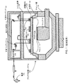
図1は、従来技術のプラズマ処理システム100の一例を示す概略断面図である。プラズマ処理システム100は、プラズマ処理チャンバを備えてよく、プラズマ処理チャンバは、プラズマ180によって示すようにプラズマを閉じ込めるために、チャンバ壁132、尖塔部(pinnacle)130、誘電体窓128などの構造要素を備えてよい。プラズマ処理チャンバ内部に、プラズマ処理システム100は、プラズマ処理中、ウエハ134によって示すようにウエハを支持するためのチャック136(静電チャックなど)を備えてよい。
FIG. 1 is a schematic cross-sectional view showing an example of a conventional
プラズマ処理システム100は、さらに、高周波(RF)電源170と、誘電体窓128上に配置され、RF電源170に電気接続された内側コイル126と、RF電源170に電気接続され、内側コイル126を取り囲む外側コイル124と、を備えてよい。内側コイル126および外側コイル124は、コイル筐体138の内部に配置されてよく、コイル筐体138は、チャンバ壁132に結合されてよい。RF電源170は、プラズマ180を生成および維持するために、内側コイル126および外側コイル124に通すRF電流を生成しうる。例えば、内側コイル126は、(内側コイル126付近の)プラズマ180の内側部分を主に維持するために第1のRF電流を流してよく、外側コイル124は、(外側コイル124付近の)プラズマ180の外側部分を主に維持するために第2のRF電流を流してよい。
The
プラズマ処理システム100は、さらに、内側コイル126および外側コイル124によって伝導されるRF電流を調節することによってプラズマ180の均一性を制御するために、電力分配器112を備えてよい。電力分配器112は、整合回路網102を介してRF電源170に電気接続されてよい。電力分配器112は、第1のRF電流のアンペア数を調節することによってプラズマ180の内側部分の密度を調節するために、RF電源170および内側コイル126の間に電気接続された可変コンデンサ116を備えてよい。電力分配器112は、第2のRF電流のアンペア数を調節することによってプラズマ180の外側部分の密度を調節するために、RF電源170および外側コイル124の間に電気接続された別の可変コンデンサ120を備えてよい。プラズマ180の異なる部分に対する別個の調節を可能にすることにより、電力分配器112は、プラズマの均一性の制御を容易にする。
The
しかしながら、電力分配器112は、いくつかの不利な点を有しうる。例えば、電力分配器112に2つの可変コンデンサ116および120が必要であるとすれば、電力分配器112の製造、維持管理、および、動作のコストは、かなり高くなりうる。現在、可変コンデンサ(可変真空コンデンサなど)には、1,000米ドルを超えるコストが掛かりうるため、電力分配器112の製造には、2,000米ドルを超えるコストが掛かりうる。さらに、可変コンデンサ116および120の各々は、かなりの維持管理および動作コストが掛かる機械部品を含みうる。また、可変コンデンサ116および120の各々は、静電容量調節を実行するように機械部品を作動させるためのステッピングモータを必要としうる。2つのステッピングモータも、電力分配器112の製造、維持管理、および、動作コストを増大させうる。結果として、電力分配器112は、プラズマ処理システム100の製造、維持管理、および、動作コストを実質的に増大させうる。
However, the power distributor 112 can have several disadvantages. For example, if the power distributor 112 requires two
2つの可変コンデンサおよび2つのステッピングモータは、実質的に多数の機械的可動部品を含みうる。実施的に多数の機械的可動部品は、プラズマ処理システム100の動作において重大な信頼性の問題を引き起こしうる。機械的可動部品のいずれかに不具合が起きると、プラズマ処理に悪影響を与え、望ましくない製品歩留まりにつながりうる。
The two variable capacitors and the two stepping motors can include a substantial number of mechanically movable parts. In practice, a large number of mechanically moving parts can cause significant reliability problems in the operation of the
さらに、既存の市販のコンデンサの限界を考えると、電力分配器112は、限られた有効電流比範囲しか提供できない。有効範囲外でプラズマ処理システム100を動作させると、不安定なプラズマ、アーク放電、整合回路網102による調整の失敗につながりうるため、製品歩留まり要件および/またはデバイスフィーチャ仕様を満たせない場合がある。
Furthermore, given the limitations of existing commercial capacitors, the power distributor 112 can only provide a limited effective current ratio range. Operating the
本発明の一実施形態は、少なくともウエハを処理するためにプラズマを生成するプラズマ処理システムに関する。プラズマ処理システムは、プラズマの少なくとも第1の部分を維持するための第1の電流を伝導するための第1のコイルを備えてよい。プラズマ処理システムは、さらに、プラズマの少なくとも第2の部分を維持するための第2の電流を伝導するための第2のコイルを備えてよい。プラズマ処理システムは、さらに、第1の電流および第2の電流を供給するための電源を備えてよい。プラズマ処理システムは、さらに、第1の電流のアンペア数および第2の電流のアンペア数の一方を調節するための並列回路を備えてよい。並列回路は、電源と第1のコイルおよび第2のコイルの少なくとも一方との間に電気接続されてよい。並列回路は、互いに並列に電気接続されたインダクタおよび可変コンデンサを備えてよい。 One embodiment of the invention relates to a plasma processing system for generating plasma to process at least a wafer. The plasma processing system may comprise a first coil for conducting a first current for maintaining at least a first portion of the plasma. The plasma processing system may further comprise a second coil for conducting a second current for maintaining at least a second portion of the plasma. The plasma processing system may further include a power source for supplying the first current and the second current. The plasma processing system may further comprise a parallel circuit for adjusting one of the first current amperage and the second current amperage. The parallel circuit may be electrically connected between the power source and at least one of the first coil and the second coil. The parallel circuit may include an inductor and a variable capacitor that are electrically connected in parallel with each other.
上述の発明の概要は、本明細書に開示された本発明の多くの実施形態の内の1つのみに関するものであり、特許請求の範囲に記載される本発明の範囲を限定する意図はない。添付の図面を参照しつつ行う本発明の詳細な説明において、本発明の上述の特徴およびその他の特徴を詳述する。 The above summary of the present invention is only relevant to one of the many embodiments of the present invention disclosed herein and is not intended to limit the scope of the present invention as recited in the claims. . The foregoing and other features of the invention are described in detail in the detailed description of the invention with reference to the accompanying drawings.
添付の図面では、限定ではなく例示を目的として本発明を図示する。なお、これらの添付図面においては、同様の構成要素には同様の符号が付されている。 The accompanying drawings illustrate the invention for purposes of illustration and not limitation. In the accompanying drawings, the same reference numerals are assigned to the same components.
以下では、添付図面に例示されたいくつかの実施形態を参照しつつ、本発明の詳細な説明を行う。以下の説明では、本発明の完全な理解を促すために、数多くの具体的な詳細事項が示されている。しかしながら、当業者にとって明らかなように、本発明は、これらの具体的な詳細事項の一部または全てがなくとも実施することが可能である。また、本発明が不必要に不明瞭となるのを避けるため、周知の処理工程および/または構造については、詳細な説明を省略した。 The present invention will be described in detail below with reference to some embodiments illustrated in the accompanying drawings. In the following description, numerous specific details are set forth in order to provide a thorough understanding of the present invention. However, it will be apparent to those skilled in the art that the present invention may be practiced without some or all of these specific details. In other instances, well known process steps and / or structures have not been described in detail in order to avoid unnecessarily obscuring the present invention.
本発明の1または複数の実施形態は、少なくとも基板を処理するためにプラズマを生成するプラズマ処理システムに関する。プラズマ処理システムは、プラズマの少なくとも第1の部分を維持するための第1の電流(例えば、RF電流)を伝導するための第1のコイルを備えてよい。プラズマ処理システムは、さらに、プラズマの少なくとも第2の部分を維持するための第2の電流(例えば、RF電流)を伝導するための第2のコイルを備えてよい。プラズマ処理システムは、さらに、第1の電流および第2の電流を供給するために第1のコイルおよび第2のコイルに電気接続された電源(例えば、RF電源)を備えてよい。プラズマ処理システムは、さらに、第1の電流と第2の電流との比を調節してプラズマの均一性を制御するために、第1の電流のアンペア数を調節するための電力分配器を備えてよい。 One or more embodiments of the invention relate to a plasma processing system that generates plasma to process at least a substrate. The plasma processing system may comprise a first coil for conducting a first current (eg, RF current) for maintaining at least a first portion of the plasma. The plasma processing system may further comprise a second coil for conducting a second current (eg, RF current) for maintaining at least a second portion of the plasma. The plasma processing system may further include a power source (eg, an RF power source) electrically connected to the first coil and the second coil to provide the first current and the second current. The plasma processing system further comprises a power divider for adjusting the amperage of the first current to adjust the ratio of the first current and the second current to control the uniformity of the plasma. It's okay.
1または複数の実施形態において、第1のコイルおよび第2のコイルは、プラズマの実質的に対称な分布を達成するために、実質的に同軸の配列に配置されてよい。1または複数の実施形態において、第1のコイルおよび第2のコイルは、特定のプラズマ分布要件を満たすために、実質的に偏心の配列に配置されてもよい。 In one or more embodiments, the first coil and the second coil may be arranged in a substantially coaxial arrangement to achieve a substantially symmetric distribution of plasma. In one or more embodiments, the first and second coils may be arranged in a substantially eccentric arrangement to meet specific plasma distribution requirements.
1または複数の実施形態において、第1のコイルは内側コイルであってよく、第2のコイルは、第1のコイルの直径よりも大きい直径を有する外側コイルであってよい。1または複数の実施形態において、第2のコイルの少なくとも一部は、第1のコイルの少なくとも一部を取り囲んでよい。 In one or more embodiments, the first coil may be an inner coil and the second coil may be an outer coil having a diameter that is greater than the diameter of the first coil. In one or more embodiments, at least a portion of the second coil may surround at least a portion of the first coil.
1または複数の実施形態において、第1のコイルは外側コイルであってよく、第2のコイルは、第1のコイルの直径よりも小さい直径を有する内側コイルであってよい。1または複数の実施形態において、第2のコイルの少なくとも一部は、第1のコイルの少なくとも一部によって取り囲まれてよい。 In one or more embodiments, the first coil may be an outer coil and the second coil may be an inner coil having a diameter that is smaller than the diameter of the first coil. In one or more embodiments, at least a portion of the second coil may be surrounded by at least a portion of the first coil.
1または複数の実施形態において、第1のコイルおよび第2のコイルは、同一平面上に配置されてよく、そうすれば、支持のためのハードウエアの設計を単純化することができ、コイルと窓のギャップ公差を一貫して制御することができる。さらに、同一平面上のコイル配置は、いくつかのプラズマ処理システムの設計にとって最適な構成でありえる。1または複数の実施形態において、特定のプラズマ処理システムの設計を考慮した場合に最適なコイル配置のために、第1のコイルが、第1の平面上に配置され、第2のコイルが、第1の平面とは異なる第2の平面上に配置されてもよい。 In one or more embodiments, the first coil and the second coil may be co-planar so that the hardware design for support can be simplified and the coil and The window gap tolerance can be controlled consistently. Furthermore, a coplanar coil arrangement may be the optimal configuration for the design of some plasma processing systems. In one or more embodiments, the first coil is disposed on the first plane and the second coil is the first coil for optimal coil placement when considering a particular plasma processing system design. You may arrange | position on the 2nd plane different from 1 plane.
電力分配器は、第1の電流のアンペア数を調節するために、電源と第1のコイルとの間のインピーダンスを変化させるための並列インダクタ−コンデンサ回路(すなわち、並列LC回路、または、タンク回路)を備えてよい。並列LC回路は、整合回路網と第1のコイルとの間、および/または、電源と第1のコイルとの間に電気接続されてよい。並列LC回路は、インダクタおよび可変コンデンサ(可変真空コンデンサまたは可変エアギャップコンデンサなど)を備えてよく、インダクタおよび可変コンデンサは、互いに並列に電気接続されてよい。 The power divider is a parallel inductor-capacitor circuit (ie, a parallel LC circuit or a tank circuit) for changing the impedance between the power source and the first coil to adjust the amperage of the first current. ) May be provided. The parallel LC circuit may be electrically connected between the matching network and the first coil and / or between the power source and the first coil. The parallel LC circuit may include an inductor and a variable capacitor (such as a variable vacuum capacitor or a variable air gap capacitor), and the inductor and the variable capacitor may be electrically connected to each other in parallel.
2つの可変コンデンサを必要とする上述の従来技術の構成例とは対照的に、本発明の実施形態では、2つのプラズマ維持コイルを備えるプラズマ処理システムにおいてプラズマの均一性を制御するのに、1つの可変コンデンサだけで足りうる。有利なことに、本発明の実施形態は、実質的に低いコストと実質的に高い信頼性を実現しうる。 In contrast to the prior art configuration example described above, which requires two variable capacitors, embodiments of the present invention provide 1 to control plasma uniformity in a plasma processing system with two plasma sustaining coils. Only one variable capacitor is enough. Advantageously, embodiments of the present invention may achieve substantially low cost and substantially high reliability.
さらに、共振効果(すなわち調和振動効果)により、並列LC回路は、整合回路網と第1のコイルと間のインピーダンスの値の範囲について、従来技術で用いられる可変コンデンサ(図1の例に示した可変コンデンサ116など)によって提供される範囲よりも実質的に広い範囲を提供しうる。結果として、本発明の実施形態は、より多い製品歩留まり要件および/またはより多いデバイスフィーチャ要件を満たすために実質的に大きい電流比の範囲を可能にしうる点で有利である。例えば、本発明の実施形態は、連続的に、負の値および正の値の間(例えば、約−0.5から約2.0までの範囲)での電流比の調節を可能にしうる。対照的に、従来技術の構成では、動作の中断、困難、または、不具合を引き起こすことなしに、正の電流比から負の電流比まで連続的に調節を行うことは実現しえない。 Furthermore, due to the resonance effect (ie harmonic vibration effect), the parallel LC circuit allows the variable capacitor (shown in the example of FIG. 1) used in the prior art for the range of impedance values between the matching network and the first coil A range that is substantially wider than that provided by variable capacitor 116, etc. may be provided. As a result, embodiments of the present invention are advantageous in that they can allow for a substantially large range of current ratios to meet more product yield requirements and / or more device feature requirements. For example, embodiments of the present invention may allow adjustment of the current ratio continuously between negative and positive values (eg, in the range of about −0.5 to about 2.0). In contrast, prior art configurations cannot achieve continuous adjustment from a positive current ratio to a negative current ratio without causing interruptions, difficulties, or failures of operation.
(高Q)並列LC回路の共振効果は、共振点周辺で制御性の問題または感度の問題を引き起こしうると一般に考えられている可能性があるため、並列LC回路の利用は、通例、プラズマ処理システムの設計および製造において避けられうる。しかしながら、インピーダンスは通例、電流の計算および/または調節時に分母に現れるため、共振点における非常に高いインピーダンスは、実際には、非常に小さい値の電流に対応しうる。その結果として、動作は、一般に考えられている制御性の問題も感度の問題も引き起こすことなく、正常な感度で(正の電流比による)通常モードから(負の電流比による)逆電流モードまで連続的に円滑でありうる。非自明な方法で、本発明の実施形態は、並列LC回路の共振効果を利用して、より広い電流比の範囲を提供し、プラズマ処理システムの制御性をさらに向上させることができる。 Since the resonance effect of a (high Q) parallel LC circuit may generally be considered to cause control problems or sensitivity problems around the resonance point, the use of parallel LC circuits is typically used for plasma processing. It can be avoided in the design and manufacture of the system. However, since impedance typically appears in the denominator during current calculation and / or adjustment, a very high impedance at the resonance point may actually correspond to a very small value of current. As a result, the operation does not cause any commonly considered controllability or sensitivity issues, but from normal mode (with positive current ratio) to reverse current mode (with negative current ratio) with normal sensitivity. Can be continuously smooth. In a non-obvious way, embodiments of the present invention can take advantage of the resonant effects of parallel LC circuits to provide a wider range of current ratios and further improve the controllability of the plasma processing system.
1または複数の実施形態において、電力分配器は、さらに、電源と第2のコイルとの間に電気接続されたさらなるインダクタを備えてよい。さらなるインダクタは、第2の電流のアンペア数を下げるためにインピーダンスを導入しうる。有利なことに、電流比の範囲は、さらに多くの製品歩留まり要件および/またはさらに多くのデバイスフィーチャ要件を満足するために、さらに拡大されうる。 In one or more embodiments, the power distributor may further comprise a further inductor electrically connected between the power source and the second coil. The further inductor may introduce impedance to reduce the amperage of the second current. Advantageously, the current ratio range can be further expanded to meet more product yield requirements and / or more device feature requirements.
本発明の特長および利点は、図面と以下の説明を参照すれば、よりよく理解できる。 The features and advantages of the present invention may be better understood with reference to the drawings and discussions that follow.
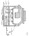
図2は、本発明の1または複数の実施形態に従って、電力分配器204を備えるプラズマ処理システム200を示す概略断面図である。プラズマ処理システム200は、図1の例で説明したプラズマ処理システム100の1または複数の構成要素と同様であっても異なっていてもよい1または複数の構成要素、例えば、プラズマ処理チャンバ、チャック、電源、コイル、コイル筐体、および/または、整合回路網などを備えてよい。特に、プラズマ処理システム200は、複数のコイルによって伝導される複数の電流間の比を調節することによってプラズマ均一性の制御を容易にするために、図1の例に示したプラズマ処理システム100の電力分配器112に鑑みて新規性および進歩性を有する電力分配器204を備えてよい。
FIG. 2 is a schematic cross-sectional view illustrating a
電力分配器204は、整合回路網206を介してRF電源270に電気接続されてよい。電力分配器204は、コイル216によって伝導される電流(例えば、RF電流)のアンペア数を調節するために、RF電源270とコイル216との間に電気接続された並列インダクタ−コンデンサ回路208(すなわち並列回路208)を備えてよい。コイル216の終端は、インピーダンス234であってよい。並列回路208は、互いに並列に電気接続されたインダクタ210および可変コンデンサ212を備えてよい。並列回路208は、タンク回路の共振効果が、整合回路網206とコイル216との間(および/または、RF電源270とコイル216との間)に広い範囲のインピーダンス値を導入できるように、タンク回路を形成しうる。したがって、電力分配器204は、コイル216によって伝導される電流のアンペア数と、コイル214として示される別のコイルによって伝導される電流のアンペア数との間の比について、広い範囲の比を実現できる。コイル214の終端は、インピーダンス234であってよい。1または複数の実施形態において、コイル214は、コイル216を取り囲んでよい。有利なことに、プラズマ処理システム200は、プラズマ処理システム100よりも多くの製品歩留まり要件および/またはデバイスフィーチャ要件を満たしうる。
The power distributor 204 may be electrically connected to the RF power source 270 via the
プラズマ処理システム100の電力分配器112が2つの可変コンデンサおよびそれらに関連する2つのステッピングモータを必要とするのに対し、電力分配器204は、1つの可変コンデンサ(すなわち、可変コンデンサ212)およびそれに関連する1つのステッピングモータだけでよい。有利なことに、電力分配器204に関連する製造、維持管理、および/または、動作のコストは、電力分配器112に関連するコストよりも実質的に低くなりうる。さらに、機械的可動部品が少ないため、電力分配器204は、電力分配器112よりも実質的に高い信頼性を有しうる。
While the power distributor 112 of the
1または複数の実施形態において、整合回路網206とコイル216との間に電気接続される代わりに、並列回路208は、例えば、異なるプラズマ均一性制御要件を満たすために、コイル214によって伝導される電流(例えば、RF電流)のアンペア数を調節するために整合回路網206とコイル214との間に電気接続されてもよい。
In one or more embodiments, instead of being electrically connected between the
コイル216によって伝導される電流とコイル214によって伝導される電流との間の比を調節するために、電力分配器204(またはプラズマ処理システム200)は、1つの並列回路すなわち1つの可変コンデンサしか必要としなくてよい。有利なことに、所望のプラズマ均一性制御を実現するに当たって、コストを最小化し、信頼性を最大化することができる。
In order to adjust the ratio between the current conducted by
プラズマ処理システム200は、さらに、RF電流比を所望の設定点に調節するために、可変コンデンサ212を駆動するための(1または複数の監視デバイスを備えてよい)制御ユニット244を備えてよい。
The
プラズマ処理システム200は、さらに、電力分配器204の最適な性能を保証するために、並列回路208を冷却するための冷却器242(例えば、冷却ファン)を備えてもよい。1または複数の実施形態において、インダクタ210は、電力損失の低い電力分配器204の最適な性能を保証するよう放熱を促進するために、銀などの高導電材料でめっきされてもよい。
The
図3は、本発明の1または複数の実施形態に従って電力分配器304の電気モデルを示す概略図である。電力分配器304は、図2の例に示したプラズマ処理システム200と同様のプラズマ処理システム内に実装されてよく、整合回路網306を通してRF電源370に電気接続されてよい。
FIG. 3 is a schematic diagram illustrating an electrical model of power distributor 304 in accordance with one or more embodiments of the present invention. The power distributor 304 may be implemented in a plasma processing system similar to the
電力分配器304は、コイル316によって伝導される電流(例えば、RF電流)のアンペア数を調節するために、RF電源370と(抵抗およびインダクタンスでモデル化された)コイル316との間に電気接続された並列インダクタ−コンデンサ回路308(すなわち並列回路308)を備えてよい。コイル316によって伝導される電流は、プラズマ処理システム内で生成されるプラズマの少なくとも一部を維持しうる。並列回路308は、互いに並列に電気接続されたインダクタ310および可変コンデンサ312を備えてよい。並列回路308は、RF電源370とコイル316との間の可能なインピーダンス値の範囲を拡大するために、共振効果を持つタンク回路を形成しうる。 The power divider 304 is electrically connected between the RF power source 370 and the coil 316 (modeled with resistance and inductance) to adjust the amperage of the current conducted by the coil 316 (eg, RF current). Parallel inductor-capacitor circuit 308 (ie, parallel circuit 308). The current conducted by the coil 316 may maintain at least a portion of the plasma generated within the plasma processing system. The parallel circuit 308 may include an inductor 310 and a variable capacitor 312 that are electrically connected in parallel to each other. The parallel circuit 308 may form a tank circuit with a resonant effect to expand the range of possible impedance values between the RF power source 370 and the coil 316.
電力分配器304は、さらに、RF電源370とコイル314との間に電気接続されたさらなるインダクタ338を備えてよく、インダクタ338および並列回路308は、互いに並列に電気接続される。インダクタ338は、コイル314によって伝導される電流のアンペア数を下げるためにインピーダンスを導入してよい(コイル314によって伝導される電流は、プラズマの少なくとも別の部分を維持しうる)。結果として、コイル314によって伝導される電流に対するコイル316によって伝導される電流の比の範囲は、プラズマ処理システムのプラズマ均一性制御能力をさらに向上させるために、さらに拡張されうる。有利なことに、さらに多くの製品歩留まり要件および/またはさらに多くのデバイスフィーチャ要件が満足されうる。 The power divider 304 may further comprise a further inductor 338 electrically connected between the RF power source 370 and the coil 314, where the inductor 338 and the parallel circuit 308 are electrically connected in parallel with each other. Inductor 338 may introduce impedance to reduce the amperage of current conducted by coil 314 (the current conducted by coil 314 may maintain at least another portion of the plasma). As a result, the range of the ratio of the current conducted by coil 316 to the current conducted by coil 314 can be further expanded to further improve the plasma uniformity control capability of the plasma processing system. Advantageously, more product yield requirements and / or more device feature requirements may be satisfied.
様々なプラズマ処理要件を満足するために、電力分配器304およびコイルの様々な接続構成が実装されてよい。1または複数の実施形態において、コイル316は、コイル314によって取り囲まれた内側コイルであってよく、コイル314は、外側コイルであってよい。1または複数の実施形態において、コイル316は、コイル314を取り囲む外側コイルであってよく、コイル314は、内側コイルであってよい。 Various connection configurations of power distributor 304 and coil may be implemented to meet various plasma processing requirements. In one or more embodiments, coil 316 may be an inner coil surrounded by coil 314, and coil 314 may be an outer coil. In one or more embodiments, the coil 316 may be an outer coil that surrounds the coil 314 and the coil 314 may be an inner coil.
図4は、本発明の1または複数の実施形態に従って電力分配器404の電気モデルを示す概略図である。電力分配器404は、図2の例に示したプラズマ処理システム200と同様のプラズマ処理システム内に実装されてよいが、繊細なプラズマ均一性制御を行うために、より多くのコイルを有する。例えば、コイルは、コイル452、コイル454、および、コイル456を含んでよく、各コイルは、抵抗およびインダクタンスとしてモデル化される。電力分配器404は、整合回路網406を介してRF電源470に電気接続されてよい。
FIG. 4 is a schematic diagram illustrating an electrical model of power distributor 404 in accordance with one or more embodiments of the present invention. The power distributor 404 may be implemented in a plasma processing system similar to the
電力分配器404は、コイル454によって伝導される電流(例えば、RF電流)のアンペア数を調節するために、RF電源470とコイル454との間に電気接続された並列インダクタ−コンデンサ回路408(すなわち並列回路408)を備えてよく、コイル454によって伝導される電流は、プラズマ処理システム内のプラズマの少なくとも第1の部分を維持しうる。電力分配器404は、さらに、コイル452によって伝導される電流(例えば、RF電流)のアンペア数を調節するために、RF電源470とコイル452との間に電気接続された並列インダクタ−コンデンサ回路414(すなわち並列回路414)を備えてよく、コイル452によって伝導される電流は、プラズマの少なくとも第2の部分を維持しうる。並列回路408および並列回路414の各々は、図2および図3の例を参照してそれぞれ上述した並列回路208および並列回路308の内の一方または両方と同様の特徴および利点を有しうる。 The power distributor 404 is a parallel inductor-capacitor circuit 408 (ie, electrically connected between the RF power source 470 and the coil 454 to adjust the amperage of the current conducted by the coil 454 (eg, RF current). A parallel circuit 408) may be provided, and the current conducted by the coil 454 may maintain at least a first portion of the plasma in the plasma processing system. The power distributor 404 further includes a parallel inductor-capacitor circuit 414 electrically connected between the RF power source 470 and the coil 452 to adjust the amperage of the current conducted by the coil 452 (eg, RF current). (Ie, a parallel circuit 414), the current conducted by the coil 452 may maintain at least a second portion of the plasma. Each of parallel circuit 408 and parallel circuit 414 may have similar features and advantages as one or both of parallel circuit 208 and parallel circuit 308 described above with reference to the examples of FIGS. 2 and 3, respectively.
電力分配器404は、さらに、RF電源470とコイル456との間に電気接続されたさらなるインダクタ438を備えてよく、インダクタ438および少なくとも並列回路414は、互いに並列に電気接続される。インダクタ438は、コイル456によって伝導される電流のアンペア数を下げるためにインピーダンスを導入してよく、コイル456によって伝導される電流は、プラズマの少なくとも第3の部分を維持しうる。結果として、コイル454によって伝導される電流とコイル456によって伝導される電流との間の差は、さらに拡大されて、コイル452によって伝導される電流とコイル456によって伝導される電流との間の差も、さらに拡大されうる。有利なことに、プラズマ処理システムのプラズマ均一性制御能力は、さらに多くの製品歩留まり要件および/またはさらに多くのデバイスフィーチャ要件を満足するよう、さらに向上されうる。 The power distributor 404 may further comprise a further inductor 438 electrically connected between the RF power source 470 and the coil 456, with the inductor 438 and at least the parallel circuit 414 being electrically connected in parallel with each other. Inductor 438 may introduce impedance to reduce the amperage of current conducted by coil 456, and the current conducted by coil 456 may maintain at least a third portion of the plasma. As a result, the difference between the current conducted by coil 454 and the current conducted by coil 456 is further magnified, and the difference between the current conducted by coil 452 and the current conducted by coil 456. Can be further expanded. Advantageously, the plasma uniformity control capability of the plasma processing system can be further improved to meet more product yield requirements and / or more device feature requirements.
様々なプラズマ処理要件を満足するために、電力分配器404およびコイルの様々な接続構成が実装されてよい。コイルは、様々な実施形態に従って、同一平面上または異なる平面上に配置されてよい。1または複数の実施形態において、コイルは、実質的に同軸の配列で配置されてよい。1または複数の実施形態において、コイル452はコイル454を取り囲んでよく、コイル454はコイル456を取り囲んでよい。1または複数の実施形態において、コイル456はコイル454を取り囲んでよく、コイル454はコイル452を取り囲んでよい。1または複数の実施形態において、コイル452はコイル456を取り囲んでよく、コイル456はコイル454を取り囲んでよい。 Various connection configurations of power distributor 404 and coils may be implemented to meet various plasma processing requirements. The coils may be arranged on the same plane or on different planes according to various embodiments. In one or more embodiments, the coils may be arranged in a substantially coaxial arrangement. In one or more embodiments, the coil 452 may surround the coil 454 and the coil 454 may surround the coil 456. In one or more embodiments, the coil 456 may surround the coil 454 and the coil 454 may surround the coil 452. In one or more embodiments, coil 452 may surround coil 456 and coil 456 may surround coil 454.
1または複数の実施形態において、プラズマ処理システムは、プラズマ均一性のさらに繊細な制御を容易にするために、プラズマの様々な部分を維持するための4つ以上のコイルを備えてよい(すなわち、コイル452、454、および、456に加えて1または複数のコイルを含んでよい)。例えば、プラズマ処理システムはN個のコイルを備えてよく、ここで、Nは4以上の整数を表す。電力分配器404は、N個のコイルの内の(N−1)個(例えば、コイル456を除いたコイル)によって伝導される電流のアンペア数を調節するための(N−1)個の並列インダクタ−コンデンサ回路を備えてよい。並列インダクタ−コンデンサ回路の各々は、RF電源470と(N−1)個のコイルの内の一つとの間に電気接続されてよい。並列インダクタ−コンデンサ回路は、図2および図3の例を参照してそれぞれ上述した並列回路208および並列回路308の内の一方または両方と同様の特徴および利点を有しうる。 In one or more embodiments, the plasma processing system may comprise four or more coils to maintain various portions of the plasma to facilitate more delicate control of plasma uniformity (ie, In addition to coils 452, 454, and 456, one or more coils may be included). For example, the plasma processing system may comprise N coils, where N represents an integer greater than or equal to 4. The power divider 404 has (N−1) parallels for adjusting the amperage of current conducted by (N−1) of the N coils (eg, the coil excluding the coil 456). An inductor-capacitor circuit may be provided. Each of the parallel inductor-capacitor circuits may be electrically connected between the RF power source 470 and one of the (N-1) coils. The parallel inductor-capacitor circuit may have features and advantages similar to one or both of the parallel circuit 208 and parallel circuit 308 described above with reference to the examples of FIGS. 2 and 3, respectively.
上記からわかるように、本発明の実施形態は、プラズマ処理システムにプラズマ均一性制御機構を実装する際に必要となる高価な可変コンデンサの数を低減することができる。有利なことに、プラズマ処理システムの製造、維持管理、および、動作コストが削減されうる。 As can be seen from the above, embodiments of the present invention can reduce the number of expensive variable capacitors required to implement a plasma uniformity control mechanism in a plasma processing system. Advantageously, the manufacturing, maintenance and operating costs of the plasma processing system can be reduced.
本発明の実施形態は、さらに、プラズマ処理システムの機械部品の数を効果的に削減しうる。有利なことに、プラズマ処理システムの信頼性が向上されうる。 Embodiments of the present invention can further effectively reduce the number of mechanical parts of the plasma processing system. Advantageously, the reliability of the plasma processing system can be improved.
本発明の実施形態は、さらに、並列LC回路の共振効果を利用して、プラズマ均一性を制御する際の電流比を大きくすることができる。有利なことに、より多い製品歩留まり要件および/またはより多いデバイスフィーチャ要件が満足されうる。 The embodiment of the present invention can further increase the current ratio when controlling the plasma uniformity by utilizing the resonance effect of the parallel LC circuit. Advantageously, more product yield requirements and / or more device feature requirements may be satisfied.
本発明の実施形態は、さらに、プラズマの異なる部分を個別に維持するために、より多くのコイルを実装することを容易にする。有利なことに、より高度なプラズマ処理システムを満足させるために、プラズマ均一性制御の精度を向上させることができる。 Embodiments of the present invention further facilitate mounting more coils to maintain different parts of the plasma separately. Advantageously, the accuracy of plasma uniformity control can be improved to satisfy a more advanced plasma processing system.
以上、いくつかの実施形態を参照しつつ本発明について説明したが、本発明の範囲内で、代替物、置換物、および、等価物が存在する。また、本発明の方法および装置を実施する他の態様が数多く存在することにも注意されたい。さらに、本発明の実施形態は、別の用途で利用されてもよい。要約書が、便宜上、提供されており、文字数の制限に従って、読み手の便宜のために記載されたもので、特許請求の範囲を限定するために用いるべきではない。したがって、以下に示す特許請求の範囲は、本発明の真の趣旨および範囲内に含まれる代替物、置換物、および、等価物の全てを網羅するものとして解釈される。
本発明は、たとえば、以下のような態様で実現することもできる。
適用例1
少なくともウエハを処理するためにプラズマを生成するプラズマ処理システムであって、
前記プラズマの少なくとも第1の部分を維持するための第1の電流を伝導する第1のコイルと、
前記プラズマの少なくとも第2の部分を維持するための第2の電流を伝導する第2のコイルと、
前記第1の電流および前記第2の電流を供給するための電源であって、前記第1のコイルおよび前記第2のコイルに電気接続されている電源と、
前記第1の電流のアンペア数および前記第2の電流のアンペア数の一方を調節するための第1の並列回路であって、前記電源と前記第1のコイルおよび前記第2のコイルの少なくとも一方との間に電気接続され、少なくとも第1のインダクタと第1の可変コンデンサとを備え、前記第1のインダクタおよび前記第1の可変コンデンサは、互いに並列に電気接続されている、第1の並列回路と、
を備える、プラズマ処理システム。
適用例2
適用例1のプラズマ処理システムであって、前記第1の電流の前記アンペア数および前記第2の電流の前記アンペア数の一方または両方を調節するための多くとも1つの可変コンデンサを備え、前記多くとも1つの可変コンデンサは、前記第1の可変コンデンサである、プラズマ処理システム。
適用例3
適用例1のプラズマ処理システムであって、前記第1の電流の前記アンペア数および前記第2の電流の前記アンペア数の一方または両方を調節するための多くとも1つの並列回路を備え、前記多くとも1つの並列回路は、前記第1の並列回路である、プラズマ処理システム。
適用例4
適用例1のプラズマ処理システムであって、
前記第1の並列回路は、前記第2の電流の前記アンペア数ではなく、前記第1の電流の前記アンペア数を調節するための並列回路であり、
前記第2のコイルは前記第1のコイルを取り囲んでいる、プラズマ処理システム。
適用例5
適用例4のプラズマ処理システムであって、さらに、前記第2の電流の前記アンペア数を下げるための第2のインダクタを備え、前記第2のインダクタは、前記電源と前記第2のコイルとの間に電気接続され、前記第2のインダクタおよび前記第1の並列回路は、互いに並列に電気接続されている、プラズマ処理システム。
適用例6
適用例1のプラズマ処理システムであって、
前記第1の並列回路は、前記第1の電流の前記アンペア数ではなく、前記第2の電流の前記アンペア数を調節するための並列回路であり、
前記第2のコイルは前記第1のコイルを取り囲んでいる、プラズマ処理システム。
適用例7
適用例6のプラズマ処理システムであって、さらに、前記第1の電流の前記アンペア数を下げるための第2のインダクタを備え、前記第2のインダクタは、前記電源と前記第1のコイルとの間に電気接続されている、プラズマ処理システム。
適用例8
適用例1のプラズマ処理システムであって、さらに、前記第1の並列回路を冷却するための冷却器を備える、プラズマ処理システム。
適用例9
適用例1のプラズマ処理システムであって、さらに、
前記プラズマの少なくとも第3の部分を維持するための第3の電流を伝導する第3のコイルであって、前記電源は前記第3の電流を供給するようにさらに構成されている、第3のコイルと、
前記第2の電流の前記アンペア数を調節するための第2の並列回路であって、前記電源と前記第2のコイルとの間に電気接続され、少なくとも第2のインダクタと第2の可変コンデンサとを備え、前記第2のインダクタおよび前記第2の可変コンデンサは、互いに並列に電気接続されている、第2の並列回路と、
を備え、
前記第1の並列回路は、前記第1の電流の前記アンペア数を調節するために前記電源と前記第1のコイルとの間に電気接続されている、プラズマ処理システム。
適用例10
適用例9のプラズマ処理システムであって、
前記第3のコイルは前記第2のコイルを取り囲んでおり、
前記第2のコイルは前記第1のコイルを取り囲んでいる、プラズマ処理システム。
適用例11
適用例9のプラズマ処理システムであって、さらに、前記第3の電流のアンペア数を下げるための第3のインダクタを備える、プラズマ処理システム。
適用例12
適用例11のプラズマ処理システムであって、
前記第3のコイルは前記第2のコイルを取り囲んでおり、
前記第2のコイルは前記第1のコイルを取り囲んでいる、プラズマ処理システム。
適用例13
適用例11のプラズマ処理システムであって、
前記第3のコイルは前記第1のコイルを取り囲んでおり、
前記第2のコイルは前記第3のコイルを取り囲んでいる、プラズマ処理システム。
適用例14
適用例11のプラズマ処理システムであって、
前記第1のコイルは前記第2のコイルを取り囲んでおり、
前記第2のコイルは前記第3のコイルを取り囲んでいる、プラズマ処理システム。
適用例15
適用例1のプラズマ処理システムであって、
前記プラズマの少なくとも複数の部分を維持するための複数の電流を伝導する複数のコイルであって、前記電源は前記複数の電流を供給するように構成され、前記複数のコイルは少なくとも前記第1のコイルおよび前記第2のコイルを含む、複数のコイルと、
前記複数の電流のアンペア数を調節するための複数の並列インダクタ−コンデンサ回路であって、前記並列インダクタ−コンデンサ回路の数は、前記コイルの数よりも1だけ少なく、少なくとも3である、プラズマ処理システム。
適用例16
適用例15のプラズマ処理システムであって、さらに、第3の電流のアンペア数を下げるための第2のインダクタを備え、前記第2のインダクタおよび前記第1のインダクタは互いに並列に電気接続され、前記第3の電流は第3のコイルによって伝導されるよう構成され、前記第2のインダクタは前記電源と前記第3のコイルとの間に電気接続され、前記電源と前記第3のコイルとの間には、前記並列インダクタ−コンデンサ回路は電気接続されない、プラズマ処理システム。
適用例17
プラズマ処理システムにおいて第2の電流のアンペア数に対する第1の電流のアンペア数の比を調節するための電力分配器であって、前記プラズマ処理システムは、プラズマの少なくとも第1の部分を維持するための前記第1の電流を伝導する第1のコイルと、前記プラズマの少なくとも第2の部分を維持するための前記第2の電流を伝導する第2のコイルと、前記第1の電流および前記第2の電流を供給するための電源とを備え、
前記電力分配器は、
前記電源と前記第1のコイルとの間に電気接続された第1のインダクタと、
前記電源と前記第1のコイルとの間に電気接続された第1の可変コンデンサと、
を備え、
前記第1のインダクタおよび前記第1の可変コンデンサは、並列に電気接続されて、第1の並列インダクタ−コンデンサ回路を形成する、電力分配器。
適用例18
適用例17の電力分配器であって、さらに、前記第2の電流の前記アンペア数を下げるための第2のインダクタを備え、前記第2のインダクタは、前記電源と前記第2のコイルとの間に電気接続され、前記第2のインダクタおよび前記第1のインダクタは、互いに並列に電気接続されている、電力分配器。
適用例19
適用例17の電力分配器であって、さらに、第2の並列インダクタ−コンデンサ回路を備え、前記第2の並列インダクタ−コンデンサ回路は、第3のコイルによって伝導される第3の電流のアンペア数を調節するために前記電源と前記第3のコイルとの間に電気接続され、第2のインダクタおよび第2の可変コンデンサを備え、前記第2のインダクタおよび前記第2の可変コンデンサは互いに並列に電気接続され、前記プラズマ処理システムはさらに前記第3のコイルを備える、電力分配器。
適用例20
適用例19の電力分配器であって、さらに、前記第2の電流の前記アンペア数を下げるための第3のインダクタを備え、前記第3のインダクタは、前記電源と前記第2のコイルとの間に電気接続され、前記第3のインダクタおよび前記第1のインダクタは、互いに並列に電気接続されている、電力分配器。
Although the present invention has been described above with reference to some embodiments, alternatives, substitutions, and equivalents exist within the scope of the present invention. It should also be noted that there are many other ways of implementing the method and apparatus of the present invention. Furthermore, embodiments of the present invention may be utilized in other applications. The abstract is provided for convenience and is provided for the convenience of the reader in accordance with the character limit and should not be used to limit the scope of the claims. Accordingly, the following claims are to be construed as covering all alternatives, substitutions, and equivalents included within the true spirit and scope of the present invention.
The present invention can also be realized in the following manner, for example.
Application example 1
A plasma processing system for generating plasma to process at least a wafer,
A first coil that conducts a first current for maintaining at least a first portion of the plasma;
A second coil conducting a second current for maintaining at least a second portion of the plasma;
A power source for supplying the first current and the second current, the power source electrically connected to the first coil and the second coil;
A first parallel circuit for adjusting one of the amperage of the first current and the amperage of the second current, wherein at least one of the power source, the first coil, and the second coil A first parallel circuit including at least a first inductor and a first variable capacitor, wherein the first inductor and the first variable capacitor are electrically connected in parallel to each other. Circuit,
A plasma processing system comprising:
Application example 2
The plasma processing system of application example 1, comprising at most one variable capacitor for adjusting one or both of the amperage of the first current and the amperage of the second current, In the plasma processing system, at least one variable capacitor is the first variable capacitor.
Application example 3
The plasma processing system of application example 1, comprising at most one parallel circuit for adjusting one or both of the amperage of the first current and the amperage of the second current, One parallel circuit is the plasma processing system, which is the first parallel circuit.
Application example 4
A plasma processing system of application example 1,
The first parallel circuit is a parallel circuit for adjusting the amperage of the first current, not the amperage of the second current,
The plasma processing system, wherein the second coil surrounds the first coil.
Application example 5
The plasma processing system according to application example 4 further includes a second inductor for reducing the amperage of the second current, and the second inductor includes a power supply and a second coil. A plasma processing system electrically connected in between, wherein the second inductor and the first parallel circuit are electrically connected in parallel with each other.
Application Example 6
A plasma processing system of application example 1,
The first parallel circuit is a parallel circuit for adjusting the amperage of the second current, not the amperage of the first current,
The plasma processing system, wherein the second coil surrounds the first coil.
Application example 7
The plasma processing system according to Application Example 6 further includes a second inductor for reducing the amperage of the first current, and the second inductor includes a power supply and a first coil. Plasma processing system with electrical connection between them.
Application example 8
The plasma processing system according to Application Example 1, further comprising a cooler for cooling the first parallel circuit.
Application example 9
The plasma processing system of application example 1, further comprising:
A third coil conducting a third current for maintaining at least a third portion of the plasma, wherein the power source is further configured to supply the third current; Coils,
A second parallel circuit for adjusting the amperage of the second current, electrically connected between the power source and the second coil, and at least a second inductor and a second variable capacitor; A second parallel circuit, wherein the second inductor and the second variable capacitor are electrically connected in parallel with each other;
With
The plasma processing system, wherein the first parallel circuit is electrically connected between the power source and the first coil to adjust the amperage of the first current.
Application Example 10
The plasma processing system of application example 9,
The third coil surrounds the second coil;
The plasma processing system, wherein the second coil surrounds the first coil.
Application Example 11
The plasma processing system according to application example 9, further comprising a third inductor for reducing the amperage of the third current.
Application Example 12
A plasma processing system according to application example 11,
The third coil surrounds the second coil;
The plasma processing system, wherein the second coil surrounds the first coil.
Application Example 13
A plasma processing system according to application example 11,
The third coil surrounds the first coil;
The plasma processing system, wherein the second coil surrounds the third coil.
Application Example 14
A plasma processing system according to application example 11,
The first coil surrounds the second coil;
The plasma processing system, wherein the second coil surrounds the third coil.
Application Example 15
A plasma processing system of application example 1,
A plurality of coils for conducting a plurality of currents for maintaining at least a plurality of portions of the plasma, wherein the power source is configured to supply the plurality of currents, the plurality of coils being at least the first A plurality of coils, including a coil and the second coil;
A plurality of parallel inductor-capacitor circuits for adjusting the amperage of the plurality of currents, wherein the number of parallel inductor-capacitor circuits is at least 3 less than the number of coils; system.
Application Example 16
The plasma processing system of application example 15 further includes a second inductor for reducing the amperage of the third current, and the second inductor and the first inductor are electrically connected in parallel to each other, The third current is configured to be conducted by a third coil, the second inductor is electrically connected between the power source and the third coil, and the power source and the third coil are connected to each other. In between, the parallel inductor-capacitor circuit is not electrically connected, the plasma processing system.
Application Example 17
A power divider for adjusting a ratio of a first current amperage to a second current amperage in a plasma processing system, wherein the plasma processing system maintains at least a first portion of a plasma. A first coil conducting the first current, a second coil conducting the second current for maintaining at least a second portion of the plasma, the first current and the first coil A power source for supplying two currents,
The power distributor is
A first inductor electrically connected between the power source and the first coil;
A first variable capacitor electrically connected between the power source and the first coil;
With
The power distributor, wherein the first inductor and the first variable capacitor are electrically connected in parallel to form a first parallel inductor-capacitor circuit.
Application Example 18
The power divider according to Application Example 17, further including a second inductor for reducing the amperage of the second current, wherein the second inductor includes a power supply and a second coil. A power distributor, electrically connected in between, wherein the second inductor and the first inductor are electrically connected in parallel with each other.
Application Example 19
The power divider according to Application Example 17, further including a second parallel inductor-capacitor circuit, wherein the second parallel inductor-capacitor circuit is an amperage of a third current conducted by a third coil. And a second inductor and a second variable capacitor, wherein the second inductor and the second variable capacitor are in parallel with each other. An electrical connection, wherein the plasma processing system further comprises the third coil.
Application Example 20
The power divider according to application example 19 further includes a third inductor for reducing the amperage of the second current, and the third inductor includes a power supply and a second coil. A power distributor electrically connected in between, wherein the third inductor and the first inductor are electrically connected in parallel with each other.
Claims (19)
前記プラズマの少なくとも第1の部分を維持するための第1の電流を伝導する第1のコイルと、
前記プラズマの少なくとも第2の部分を維持するための第2の電流を伝導する第2のコイルと、
前記第1の電流および前記第2の電流を供給するための電源であって、前記第1のコイルおよび前記第2のコイルに電気接続されている電源と、
前記第1の電流のアンペア数および前記第2の電流のアンペア数の一方を調節するための第1の並列回路であって、前記電源と前記第1のコイルおよび前記第2のコイルの少なくとも一方との間に電気接続され、少なくとも第1のインダクタと第1の可変コンデンサとを備え、前記第1のインダクタおよび前記第1の可変コンデンサは、互いに並列に電気接続されている、第1の並列回路と、
を備え、
前記プラズマ処理システムは、前記第1の電流の前記アンペア数および前記第2の電流の前記アンペア数の一方または両方を調節するための多くとも1つの可変コンデンサを備え、前記多くとも1つの可変コンデンサは、前記第1の可変コンデンサである、プラズマ処理システム。 A plasma processing system for generating plasma to process at least a wafer,
A first coil that conducts a first current for maintaining at least a first portion of the plasma;
A second coil conducting a second current for maintaining at least a second portion of the plasma;
A power source for supplying the first current and the second current, the power source electrically connected to the first coil and the second coil;
A first parallel circuit for adjusting one of the amperage of the first current and the amperage of the second current, wherein at least one of the power source, the first coil, and the second coil A first parallel circuit including at least a first inductor and a first variable capacitor, wherein the first inductor and the first variable capacitor are electrically connected in parallel to each other. Circuit,
Equipped with a,
The plasma processing system comprises at most one variable capacitor for adjusting one or both of the amperage of the first current and the amperage of the second current, the at least one variable capacitor Is a plasma processing system which is the first variable capacitor.
前記第1の並列回路は、前記第2の電流の前記アンペア数ではなく、前記第1の電流の前記アンペア数を調節するための並列回路であり、
前記第2のコイルは前記第1のコイルを取り囲んでいる、プラズマ処理システム。 The plasma processing system according to claim 1,
The first parallel circuit is a parallel circuit for adjusting the amperage of the first current, not the amperage of the second current,
The plasma processing system, wherein the second coil surrounds the first coil.
前記第1の並列回路は、前記第1の電流の前記アンペア数ではなく、前記第2の電流の前記アンペア数を調節するための並列回路であり、
前記第2のコイルは前記第1のコイルを取り囲んでいる、プラズマ処理システム。 The plasma processing system according to claim 1,
The first parallel circuit is a parallel circuit for adjusting the amperage of the second current, not the amperage of the first current,
The plasma processing system, wherein the second coil surrounds the first coil.
前記プラズマの少なくとも第3の部分を維持するための第3の電流を伝導する第3のコイルであって、前記電源は前記第3の電流を供給するようにさらに構成されている、第3のコイルと、
前記第2の電流の前記アンペア数を調節するための第2の並列回路であって、前記電源と前記第2のコイルとの間に電気接続され、少なくとも第2のインダクタと第2の可変コンデンサとを備え、前記第2のインダクタおよび前記第2の可変コンデンサは、互いに並列に電気接続されている、第2の並列回路と、
を備え、
前記第1の並列回路は、前記第1の電流の前記アンペア数を調節するために前記電源と前記第1のコイルとの間に電気接続されている、プラズマ処理システム。 The plasma processing system of claim 1, further comprising:
A third coil conducting a third current for maintaining at least a third portion of the plasma, wherein the power source is further configured to supply the third current; Coils,
A second parallel circuit for adjusting the amperage of the second current, electrically connected between the power source and the second coil, and at least a second inductor and a second variable capacitor; A second parallel circuit, wherein the second inductor and the second variable capacitor are electrically connected in parallel with each other;
With
The plasma processing system, wherein the first parallel circuit is electrically connected between the power source and the first coil to adjust the amperage of the first current.
前記第3のコイルは前記第2のコイルを取り囲んでおり、
前記第2のコイルは前記第1のコイルを取り囲んでいる、プラズマ処理システム。 The plasma processing system according to claim 8 ,
The third coil surrounds the second coil;
The plasma processing system, wherein the second coil surrounds the first coil.
前記第3のコイルは前記第2のコイルを取り囲んでおり、
前記第2のコイルは前記第1のコイルを取り囲んでいる、プラズマ処理システム。 The plasma processing system of claim 1 0,
The third coil surrounds the second coil;
The plasma processing system, wherein the second coil surrounds the first coil.
前記第3のコイルは前記第1のコイルを取り囲んでおり、
前記第2のコイルは前記第3のコイルを取り囲んでいる、プラズマ処理システム。 The plasma processing system of claim 1 0,
The third coil surrounds the first coil;
The plasma processing system, wherein the second coil surrounds the third coil.
前記第1のコイルは前記第2のコイルを取り囲んでおり、
前記第2のコイルは前記第3のコイルを取り囲んでいる、プラズマ処理システム。 The plasma processing system of claim 1 0,
The first coil surrounds the second coil;
The plasma processing system, wherein the second coil surrounds the third coil.
前記プラズマの少なくとも複数の部分を維持するための複数の電流を伝導する複数のコイルであって、前記電源は前記複数の電流を供給するように構成され、前記複数のコイルは少なくとも前記第1のコイルおよび前記第2のコイルを含む、複数のコイルと、
前記複数の電流のアンペア数を調節するための複数の並列インダクタ−コンデンサ回路であって、前記並列インダクタ−コンデンサ回路の数は、前記コイルの数よりも1だけ少なく、少なくとも3である、プラズマ処理システム。 The plasma processing system according to claim 1,
A plurality of coils for conducting a plurality of currents for maintaining at least a plurality of portions of the plasma, wherein the power source is configured to supply the plurality of currents, the plurality of coils being at least the first A plurality of coils, including a coil and the second coil;
A plurality of parallel inductor-capacitor circuits for adjusting the amperage of the plurality of currents, wherein the number of parallel inductor-capacitor circuits is at least 3 less than the number of coils; system.
前記電力分配器は、
前記電源と前記第1のコイルとの間に電気接続された第1のインダクタと、
前記電源と前記第1のコイルとの間に電気接続された第1の可変コンデンサと、
を備え、
前記第1のインダクタおよび前記第1の可変コンデンサは、並列に電気接続されて、第1の並列インダクタ−コンデンサ回路を形成し、
前記電力分配器は、前記第1の電流の前記アンペア数および前記第2の電流の前記アンペア数の一方または両方を調節するための多くとも1つの可変コンデンサを備え、前記多くとも1つの可変コンデンサは、前記第1の可変コンデンサである、電力分配器。 A power divider for adjusting a ratio of a first current amperage to a second current amperage in a plasma processing system, wherein the plasma processing system maintains at least a first portion of a plasma. A first coil conducting the first current, a second coil conducting the second current for maintaining at least a second portion of the plasma, the first current and the first coil A power source for supplying two currents,
The power distributor is
A first inductor electrically connected between the power source and the first coil;
A first variable capacitor electrically connected between the power source and the first coil;
With
Said first inductor and said first variable capacitor is in parallel is electrically connected, the first parallel inductor - form a capacitor circuit,
The power divider comprises at most one variable capacitor for adjusting one or both of the amperage of the first current and the amperage of the second current, the at least one variable capacitor Is a power distributor which is the first variable capacitor.
Applications Claiming Priority (3)
| Application Number | Priority Date | Filing Date | Title |
|---|---|---|---|
| US18671009P | 2009-06-12 | 2009-06-12 | |
| US61/186,710 | 2009-06-12 | ||
| PCT/US2010/037942 WO2010144555A2 (en) | 2009-06-12 | 2010-06-09 | Adjusting current ratios in inductively coupled plasma processing systems |
Publications (3)
| Publication Number | Publication Date |
|---|---|
| JP2012529750A JP2012529750A (en) | 2012-11-22 |
| JP2012529750A5 JP2012529750A5 (en) | 2013-07-25 |
| JP5643301B2 true JP5643301B2 (en) | 2014-12-17 |
Family
ID=43305377
Family Applications (1)
| Application Number | Title | Priority Date | Filing Date |
|---|---|---|---|
| JP2012515098A Active JP5643301B2 (en) | 2009-06-12 | 2010-06-09 | Plasma processing system and power distributor |
Country Status (7)
| Country | Link |
|---|---|
| US (1) | US9305750B2 (en) |
| JP (1) | JP5643301B2 (en) |
| KR (1) | KR101708075B1 (en) |
| CN (1) | CN102804930A (en) |
| SG (2) | SG10201402467SA (en) |
| TW (1) | TW201127224A (en) |
| WO (1) | WO2010144555A2 (en) |
Families Citing this family (30)
| Publication number | Priority date | Publication date | Assignee | Title |
|---|---|---|---|---|
| US8501631B2 (en) * | 2009-11-19 | 2013-08-06 | Lam Research Corporation | Plasma processing system control based on RF voltage |
| JPWO2011102083A1 (en) * | 2010-02-19 | 2013-06-17 | 株式会社アルバック | Plasma processing apparatus and plasma processing method |
| JP5781349B2 (en) | 2011-03-30 | 2015-09-24 | 東京エレクトロン株式会社 | Plasma processing equipment |
| US10056231B2 (en) * | 2011-04-28 | 2018-08-21 | Lam Research Corporation | TCCT match circuit for plasma etch chambers |
| US9320126B2 (en) | 2012-12-17 | 2016-04-19 | Lam Research Corporation | Determining a value of a variable on an RF transmission model |
| US9197196B2 (en) | 2012-02-22 | 2015-11-24 | Lam Research Corporation | State-based adjustment of power and frequency |
| US10128090B2 (en) | 2012-02-22 | 2018-11-13 | Lam Research Corporation | RF impedance model based fault detection |
| US10157729B2 (en) | 2012-02-22 | 2018-12-18 | Lam Research Corporation | Soft pulsing |
| US9462672B2 (en) | 2012-02-22 | 2016-10-04 | Lam Research Corporation | Adjustment of power and frequency based on three or more states |
| US9114666B2 (en) | 2012-02-22 | 2015-08-25 | Lam Research Corporation | Methods and apparatus for controlling plasma in a plasma processing system |
| US9842725B2 (en) | 2013-01-31 | 2017-12-12 | Lam Research Corporation | Using modeling to determine ion energy associated with a plasma system |
| CN103060778B (en) * | 2013-01-23 | 2015-03-11 | 深圳市劲拓自动化设备股份有限公司 | Flat plate type PECVD (Plasma Enhanced Chemical Vapor Deposition) device |
| KR20140122548A (en) * | 2013-04-10 | 2014-10-20 | 피에스케이 주식회사 | Apparatus and method for providing power, and apparatus for treating substrate using the same |
| KR102175081B1 (en) * | 2013-12-27 | 2020-11-06 | 세메스 주식회사 | Plasma generating device and apparatus for treating substrate comprising the same |
| US9594105B2 (en) | 2014-01-10 | 2017-03-14 | Lam Research Corporation | Cable power loss determination for virtual metrology |
| US10950421B2 (en) | 2014-04-21 | 2021-03-16 | Lam Research Corporation | Using modeling for identifying a location of a fault in an RF transmission system for a plasma system |
| CN104332379B (en) * | 2014-09-02 | 2017-12-19 | 清华大学 | Plasma discharge apparatus |
| US9515633B1 (en) * | 2016-01-11 | 2016-12-06 | Lam Research Corporation | Transformer coupled capacitive tuning circuit with fast impedance switching for plasma etch chambers |
| US9839109B1 (en) * | 2016-05-30 | 2017-12-05 | Applied Materials, Inc. | Dynamic control band for RF plasma current ratio control |
| US10553465B2 (en) * | 2016-07-25 | 2020-02-04 | Lam Research Corporation | Control of water bow in multiple stations |
| CN108271307B (en) * | 2016-12-30 | 2019-11-05 | 中微半导体设备(上海)股份有限公司 | Inductance coupling plasma processing device and plasma generating device |
| CN108882494B (en) * | 2017-05-08 | 2022-06-17 | 北京北方华创微电子装备有限公司 | Plasma device |
| CN111699542B (en) | 2017-11-29 | 2023-05-16 | 康姆艾德技术美国分公司 | Retuning for impedance matching network control |
| CN111192752B (en) * | 2018-11-14 | 2021-08-31 | 江苏鲁汶仪器有限公司 | Power distribution inductive coupling coil and plasma processing device with same |
| CN111199860A (en) * | 2018-11-20 | 2020-05-26 | 江苏鲁汶仪器有限公司 | Etching uniformity adjusting device and method |
| US11114279B2 (en) * | 2019-06-28 | 2021-09-07 | COMET Technologies USA, Inc. | Arc suppression device for plasma processing equipment |
| US11107661B2 (en) | 2019-07-09 | 2021-08-31 | COMET Technologies USA, Inc. | Hybrid matching network topology |
| US11342887B2 (en) * | 2019-12-18 | 2022-05-24 | Nxp Usa, Inc. | Wideband RF power splitters and amplifiers including wideband RF power splitters |
| KR102147877B1 (en) * | 2020-04-01 | 2020-08-25 | 주식회사 기가레인 | Plasma antena module |
| CN113496863B (en) * | 2020-04-01 | 2022-04-12 | 吉佳蓝科技股份有限公司 | Plasma antenna module |
Family Cites Families (15)
| Publication number | Priority date | Publication date | Assignee | Title |
|---|---|---|---|---|
| TW293983B (en) * | 1993-12-17 | 1996-12-21 | Tokyo Electron Co Ltd | |
| US5907221A (en) * | 1995-08-16 | 1999-05-25 | Applied Materials, Inc. | Inductively coupled plasma reactor with an inductive coil antenna having independent loops |
| US6054013A (en) | 1996-02-02 | 2000-04-25 | Applied Materials, Inc. | Parallel plate electrode plasma reactor having an inductive antenna and adjustable radial distribution of plasma ion density |
| KR100601749B1 (en) | 1997-11-10 | 2006-07-19 | 제온 코포레이션 | Binder containing vinyl alcohol polymer, slurry, electrode, and secondary battery with nonaqueous electrolyte |
| US6326597B1 (en) * | 1999-04-15 | 2001-12-04 | Applied Materials, Inc. | Temperature control system for process chamber |
| KR100338057B1 (en) * | 1999-08-26 | 2002-05-24 | 황 철 주 | Antenna device for generating inductively coupled plasma |
| US6507155B1 (en) | 2000-04-06 | 2003-01-14 | Applied Materials Inc. | Inductively coupled plasma source with controllable power deposition |
| JP2003100723A (en) | 2001-09-27 | 2003-04-04 | Tokyo Electron Ltd | Inductive coupled plasma processing apparatus |
| US6876155B2 (en) * | 2002-12-31 | 2005-04-05 | Lam Research Corporation | Plasma processor apparatus and method, and antenna |
| KR101144018B1 (en) * | 2004-05-28 | 2012-05-09 | 램 리써치 코포레이션 | Plasma processor with electrode responsive to multiple rf frequencies |
| KR100648336B1 (en) * | 2004-07-12 | 2006-11-23 | 어플라이드 머티어리얼스, 인코포레이티드 | Apparatus and methods for a fixed impedance transformation network for use in connection with a plasma chamber |
| JP4884901B2 (en) | 2006-09-21 | 2012-02-29 | 三菱重工業株式会社 | Thin film manufacturing apparatus and solar cell manufacturing method |
| KR100898165B1 (en) | 2006-11-24 | 2009-05-19 | 엘지전자 주식회사 | Apparatus and method for generation a plasma |
| KR20080102615A (en) * | 2007-05-21 | 2008-11-26 | 네스트 주식회사 | Method and apparatus for multi-mode plasma generation |
| JP5329167B2 (en) | 2007-11-21 | 2013-10-30 | 東京エレクトロン株式会社 | Inductively coupled plasma processing apparatus, inductively coupled plasma processing method, and storage medium |
-
2010
- 2010-03-19 US US12/728,112 patent/US9305750B2/en active Active
- 2010-06-09 JP JP2012515098A patent/JP5643301B2/en active Active
- 2010-06-09 WO PCT/US2010/037942 patent/WO2010144555A2/en active Application Filing
- 2010-06-09 KR KR1020117029647A patent/KR101708075B1/en active IP Right Grant
- 2010-06-09 SG SG10201402467SA patent/SG10201402467SA/en unknown
- 2010-06-09 CN CN2010800262057A patent/CN102804930A/en active Pending
- 2010-06-09 SG SG2011083961A patent/SG176069A1/en unknown
- 2010-06-11 TW TW99119079A patent/TW201127224A/en unknown
Also Published As
| Publication number | Publication date |
|---|---|
| US9305750B2 (en) | 2016-04-05 |
| US20100314048A1 (en) | 2010-12-16 |
| WO2010144555A3 (en) | 2011-02-24 |
| TW201127224A (en) | 2011-08-01 |
| KR101708075B1 (en) | 2017-02-17 |
| WO2010144555A2 (en) | 2010-12-16 |
| SG176069A1 (en) | 2011-12-29 |
| CN102804930A (en) | 2012-11-28 |
| KR20120028916A (en) | 2012-03-23 |
| JP2012529750A (en) | 2012-11-22 |
| SG10201402467SA (en) | 2014-09-26 |
Similar Documents
| Publication | Publication Date | Title |
|---|---|---|
| JP5643301B2 (en) | Plasma processing system and power distributor | |
| CN109104807B (en) | Plasma processing apparatus | |
| JP6374489B2 (en) | High speed vacuum variable capacitor | |
| US8742666B2 (en) | Radio frequency (RF) power filters and plasma processing systems including RF power filters | |
| US20150243486A1 (en) | Plasma processing apparatus | |
| KR20110058699A (en) | Plasma processing apparatus | |
| KR20200053622A (en) | RF filter for multi-frequency RF (radiofrequency) bias | |
| US6473289B1 (en) | Vacuum variable capacitor | |
| JP7117725B2 (en) | Inductor, device with inductor, and method for manufacturing inductor | |
| US10651813B2 (en) | Method for designing filter | |
| JP5595136B2 (en) | Inductively coupled plasma generator | |
| KR20130140571A (en) | Plasma processing apparatus, plasma producing apparatus, antenna structure, and plasma producing method | |
| JP2002124399A (en) | Plasma generation device | |
| EP3005386B1 (en) | Vacuum variable capacitor | |
| US11251021B2 (en) | Mode-switching plasma systems and methods of operating thereof | |
| WO2020247135A1 (en) | Variable inductor device |
Legal Events
| Date | Code | Title | Description |
|---|---|---|---|
| A521 | Request for written amendment filed |
Free format text: JAPANESE INTERMEDIATE CODE: A523 Effective date: 20130604 |
|
| A621 | Written request for application examination |
Free format text: JAPANESE INTERMEDIATE CODE: A621 Effective date: 20130604 |
|
| A977 | Report on retrieval |
Free format text: JAPANESE INTERMEDIATE CODE: A971007 Effective date: 20140318 |
|
| A131 | Notification of reasons for refusal |
Free format text: JAPANESE INTERMEDIATE CODE: A131 Effective date: 20140401 |
|
| A521 | Request for written amendment filed |
Free format text: JAPANESE INTERMEDIATE CODE: A523 Effective date: 20140630 |
|
| TRDD | Decision of grant or rejection written | ||
| A01 | Written decision to grant a patent or to grant a registration (utility model) |
Free format text: JAPANESE INTERMEDIATE CODE: A01 Effective date: 20141007 |
|
| A61 | First payment of annual fees (during grant procedure) |
Free format text: JAPANESE INTERMEDIATE CODE: A61 Effective date: 20141030 |
|
| R150 | Certificate of patent or registration of utility model |
Ref document number: 5643301 Country of ref document: JP Free format text: JAPANESE INTERMEDIATE CODE: R150 |
|
| R250 | Receipt of annual fees |
Free format text: JAPANESE INTERMEDIATE CODE: R250 |
|
| R250 | Receipt of annual fees |
Free format text: JAPANESE INTERMEDIATE CODE: R250 |
|
| R250 | Receipt of annual fees |
Free format text: JAPANESE INTERMEDIATE CODE: R250 |
|
| R250 | Receipt of annual fees |
Free format text: JAPANESE INTERMEDIATE CODE: R250 |
|
| R250 | Receipt of annual fees |
Free format text: JAPANESE INTERMEDIATE CODE: R250 |
|
| R250 | Receipt of annual fees |
Free format text: JAPANESE INTERMEDIATE CODE: R250 |
|
| R250 | Receipt of annual fees |
Free format text: JAPANESE INTERMEDIATE CODE: R250 |