JP5638357B2 - Copper alloy for electrical and electronic parts and method for producing the same - Google Patents
Copper alloy for electrical and electronic parts and method for producing the same Download PDFInfo
- Publication number
- JP5638357B2 JP5638357B2 JP2010257995A JP2010257995A JP5638357B2 JP 5638357 B2 JP5638357 B2 JP 5638357B2 JP 2010257995 A JP2010257995 A JP 2010257995A JP 2010257995 A JP2010257995 A JP 2010257995A JP 5638357 B2 JP5638357 B2 JP 5638357B2
- Authority
- JP
- Japan
- Prior art keywords
- less
- particles
- copper alloy
- hours
- electrical
- Prior art date
- Legal status (The legal status is an assumption and is not a legal conclusion. Google has not performed a legal analysis and makes no representation as to the accuracy of the status listed.)
- Active
Links
Images

Description
本発明は、電気・電子部品用銅合金およびその製造方法に係り、特にリードフレーム、端子、コネクタ等の電気・電子部品に好適な強度や導電性に優れる電気・電子部品用銅合金およびその製造方法に関するものである。 The present invention relates to a copper alloy for electric / electronic parts and a method for producing the same, and particularly to a copper alloy for electric / electronic parts having excellent strength and conductivity suitable for electric / electronic parts such as lead frames, terminals and connectors, and the production thereof. It is about the method.
電子機器に用いられる半導体製品は大容量、小型化、高機能化にともない、これに使用されるリードフレームも多ピン化、薄肉化が進み、一層の強度、導電性が要求されてきている。このような要求に対し、これらの特性を比較的良好に満足する材料としてCu−2.2重量%Fe−0.03重量%P−0.12重量%Znを標準化学組成とする銅合金(CDA Alloy 194)が挙げられる(例えば、特許文献1参照)。 As semiconductor products used in electronic devices have larger capacities, smaller sizes, and higher functions, lead frames used for these products have become increasingly multi-pin and thinner, and further strength and conductivity have been required. In response to such requirements, a copper alloy having a standard chemical composition of Cu-2.2 wt% Fe-0.03% wt P-0.12 wt% Zn as a material that satisfies these characteristics relatively well ( CDA Alloy 194) (for example, refer to Patent Document 1).
しかし、リードフレームの多ピン化、薄肉化に伴い、素材からリードフレームへの打ち抜き加工の際に生じる歪が大きくなってきている。その歪を除去するために焼鈍を必要とされる状況において、上記銅合金では耐熱性が不十分であり、リードフレームにおける歪取りのための焼鈍による強度低下が問題である。端子、コネクタなど他の電気・電子部品においても、電子機器の小型化によって素材の加工による歪蓄積が大きくなり、同様の問題がある。 However, with the increase in the number of pins and the thinning of the lead frame, the distortion that occurs during the punching process from the material to the lead frame is increasing. In a situation where annealing is required to remove the strain, the copper alloy has insufficient heat resistance, and there is a problem of strength reduction due to annealing for strain relief in the lead frame. Other electrical / electronic parts such as terminals and connectors also have the same problem due to the increased strain accumulation due to the processing of materials due to the downsizing of electronic equipment.
そこで、この銅合金の耐熱性を改善するために、例えば、40nm以下のFe粒子を、体積率0.2%以上で分散させてピン止め粒として作用させ、回復・再結晶を遅延させる手法(例えば、特許文献2参照)が提案されている。 Therefore, in order to improve the heat resistance of the copper alloy, for example, a method of delaying recovery / recrystallization by dispersing Fe particles of 40 nm or less at a volume ratio of 0.2% or more and acting as pinning grains ( For example, see Patent Document 2).
しかし、より耐熱性が要求される状況においては、特許文献2のピン止め効果による回復・再結晶の遅延だけでは、なお不十分である。 However, in a situation where more heat resistance is required, the recovery / recrystallization delay due to the pinning effect of Patent Document 2 is still insufficient.
そこで、本発明の目的は、高強度、高導電性を有すると共に、耐熱性に優れた電気・電子部品用銅合金およびその製造方法を提供することにある。 SUMMARY OF THE INVENTION An object of the present invention is to provide a copper alloy for electric / electronic parts having high strength and high conductivity and excellent heat resistance, and a method for producing the same.
本発明の第一の様態によれば、Feを2.0重量%以上2.6重量%以下、Pを0.01重量%以上0.2重量%以下、Znを0.01重量%以上1.0重量%以下含有し、残部がCuと不可避的不純物からなる電気・電子部品用銅合金において、
銅母相中に分散するFeを含有する粒子の中で、直径が50nmより大きい粒子の数密度N1と、直径が50nm以下である粒子の数密度N2との比N2/N1が5以上であり、
直径が20nm以上50nm以下の粒子における平均粒子間隔が50nm以上300nm以下である電気・電子部品用銅合金が提供される。
According to the first aspect of the present invention, Fe is 2.0 wt% or more and 2.6 wt% or less, P is 0.01 wt% or more and 0.2 wt% or less, Zn is 0.01 wt% or more and 1 wt% or less. In a copper alloy for electrical and electronic parts that contains 0.0% by weight or less and the balance is Cu and inevitable impurities,
Among the particles containing Fe dispersed in the copper matrix, the ratio N 2 / N 1 of the number density N 1 of particles having a diameter larger than 50 nm and the number density N 2 of particles having a diameter of 50 nm or less is 5 or more
Provided is a copper alloy for electric / electronic parts having an average particle spacing of 50 nm to 300 nm in particles having a diameter of 20 nm to 50 nm.
本発明の第二の様態によれば、Feを2.0重量%以上2.6重量%以下、Pを0.0
1重量%以上0.2重量%以下、Znを0.01重量%以上1重量%以下含有し、残部がCuと不可避的不純物からなる鋳塊を、圧延工程と熱処理工程とを組み合わせて所望の板厚まで加工する電気・電子部品用銅合金の製造方法において、
前記熱処理工程では、500℃以上550℃以下の温度で、30分以上6時間以下の時間で熱処理をし、
その後、更に400℃以上480℃以下の温度で、1時間以上8時間以下の時間で熱処理をする電気・電子部品用銅合金の製造方法が提供される。
According to the second aspect of the present invention, Fe is 2.0 wt% or more and 2.6 wt% or less, and P is 0.0 wt%.
An ingot containing 1% by weight or more and 0.2% by weight or less, Zn of 0.01% by weight or more and 1% by weight or less, with the balance being Cu and inevitable impurities, is combined with a rolling process and a heat treatment process to obtain a desired ingot. In the method of manufacturing a copper alloy for electrical and electronic parts that is processed to a plate thickness,
In the heat treatment step, heat treatment is performed at a temperature of 500 ° C. or more and 550 ° C. or less for a time of 30 minutes or more and 6 hours or less,
Then, the manufacturing method of the copper alloy for electrical / electronic components which heat-processes at the temperature of 400 to 480 degreeC further for 1 hour or more and 8 hours or less is provided.
本発明によれば、高強度、高導電性を有すると共に、耐熱性に優れた電気・電子部品用銅合金およびその製造方法を提供することができる。 ADVANTAGE OF THE INVENTION According to this invention, while having high intensity | strength and high electroconductivity, it can provide the copper alloy for electrical / electronic components excellent in heat resistance, and its manufacturing method.
以下に本発明の一実施の形態に係る電気・電子部品用銅合金およびその製造方法について述べる。 The copper alloy for electric / electronic parts and the manufacturing method thereof according to one embodiment of the present invention will be described below.
電気・電子部品用銅合金
本実施の形態の銅合金は、Cu−Fe−P合金(CDA Alloy 194)である。このCu−Fe−P合金において、優れた耐熱性とは、ある温度、時間で焼鈍した場合に低下する強度が小さいことを表している。素材的にみれば、焼鈍過程の強度低下は回復・再結晶といわれる現象に起因すると考えられる。ここで、回復も再結晶も銅母相の歪解消現象であり、加熱等で発生する現象である。回復と再結晶の違いは、前者が歪の原因である転位(ナノレベルの材料欠陥の1つ)自身が動いて再配列することで歪を小さくするのに対し、後者は銅母相の粒界が転位を吸収することで歪を小さくすることである。なお、再結晶は結晶粒界移動現象(駆動力が転位等による歪エネルギー)のため、銅母相の結晶粒は粗大になっていく。
Copper alloy for electric / electronic parts The copper alloy of the present embodiment is a Cu-Fe-P alloy (CDA Alloy 194). In this Cu—Fe—P alloy, excellent heat resistance means that the strength that decreases when annealed at a certain temperature and time is small. From the viewpoint of materials, it is considered that the strength reduction in the annealing process is caused by a phenomenon called recovery / recrystallization. Here, both recovery and recrystallization are phenomena of eliminating distortion of the copper matrix phase, and are phenomena that occur due to heating or the like. The difference between recovery and recrystallization is that the former is a dislocation (one of nano-level material defects) that causes the strain itself to move and rearrange itself, while the latter reduces the strain of the copper matrix. The field is to reduce the strain by absorbing dislocations. In addition, since recrystallization is a crystal grain boundary movement phenomenon (the driving force is strain energy due to dislocations or the like), the crystal grains of the copper matrix phase become coarse.
このように強度低下は回復・再結晶に起因するため、耐熱性を改善するためには回復・再結晶を遅延させればよいといえる。本ターゲットであるCu−Fe−P合金を透過電子顕微鏡で観察した結果、回復・再結晶の起点は50nmより大きい粒子に接した場所であり、またそのサイズは粗大で300nmより大きい。 Thus, since the strength reduction is caused by recovery / recrystallization, it can be said that the recovery / recrystallization may be delayed in order to improve the heat resistance. As a result of observing the target Cu—Fe—P alloy with a transmission electron microscope, the starting point of recovery / recrystallization is a place in contact with particles larger than 50 nm, and the size is coarse and larger than 300 nm.
このため、再結晶による強度低下については、銅母相中に分散する50nmより大きい粒子を極力少なくすることが重要となる。さらに、再結晶の起点とならない粒子の平均間隔を300nm以下にすることで、再結晶核が生成された場合でも、ピン止めによって再結晶の成長を抑制することも重要となる。ここで、ピン止めとは析出物などを銅母相中に分散させることで銅母相中の結晶粒界の移動を抑制できる効果であり、再結晶が発生してもその粒界移動を抑え、再結晶粒の粗大化抑制を期待できるものである。 For this reason, it is important to reduce the number of particles larger than 50 nm dispersed in the copper matrix as much as possible for the strength reduction due to recrystallization. Furthermore, it is also important to suppress the growth of recrystallization by pinning even when recrystallization nuclei are generated by setting the average interval of particles not serving as the starting point of recrystallization to 300 nm or less. Here, pinning is an effect that suppresses the movement of crystal grain boundaries in the copper matrix phase by dispersing precipitates in the copper matrix phase, and suppresses the grain boundary migration even if recrystallization occurs. It can be expected to suppress the coarsening of recrystallized grains.
また、回復による強度低下については、Fe析出物の整合性を維持することでその発生を抑制することが重要となる。Fe粒子は加工を加えると整合という状態から非整合という状態に変化する。また、非整合のFe粒子は転位を引きつける特性があると報告されている(整合粒子の場合転位との間に斥力が働く)。このことから、非整合のFe粒子はこれと銅母相の界面にて他の場所よりも転位が増加しやすいと考えられる。転位の増加は回復・再結晶の駆動力を大きくするので、加熱時に回復・再結晶を促進し、軟化しやすくなる起点になると考えられる。このため、Fe析出物の整合性を維持することが必要となる
。
In addition, it is important to suppress the occurrence of strength reduction due to recovery by maintaining the consistency of Fe precipitates. When the Fe particles are processed, the state changes from the aligned state to the non-aligned state. Further, it is reported that non-matched Fe particles have a property of attracting dislocations (in the case of matched particles, repulsive force acts between the dislocations). From this, it is considered that dislocations of non-matching Fe particles are likely to increase in dislocations at the interface between the non-matching Fe particles and the copper matrix phase than at other places. An increase in dislocations increases the driving force for recovery / recrystallization, and is considered to be a starting point that facilitates recovery / recrystallization during heating and becomes easy to soften. For this reason, it is necessary to maintain the consistency of the Fe precipitate.
本実施の形態の銅合金は、後述する第三冷間圧延による加工硬化(結晶微細化と転位強化)が合金強度を得る手段の一つであるため、回復・再結晶が発生してしまうと強度が低下する。回復・再結晶は上記のとおり加熱で発生する現象であるので、これが容易に発生すると、例えば顧客先のリードフレーム製造工程に含まれる歪取り焼鈍を加えることにより強度が低下してしまう。このリードフレーム製造工程での強度低下はリードフレームのピンなどの剛性不足などの不具合の原因となるので、これを防ぐ必要がある。 In the copper alloy of the present embodiment, work hardening (crystal refinement and dislocation strengthening) by third cold rolling, which will be described later, is one of means for obtaining alloy strength, so that recovery / recrystallization occurs. Strength decreases. Since recovery / recrystallization is a phenomenon that occurs by heating as described above, if this occurs easily, the strength decreases due to, for example, applying strain relief annealing included in the lead frame manufacturing process of the customer. This decrease in strength in the lead frame manufacturing process causes problems such as insufficient rigidity of the lead frame pins and the like, and it is necessary to prevent this.
この対策として、本実施の形態では、整合のFe析出物を分散させるという合金制御を行うことで、回復・再結晶を抑制し、ピン止め効果による回復・再結晶の遅延だけでは不十分であった加熱(耐熱試験)による強度低下を防ぎ、耐熱性を高めている。 As a countermeasure, in this embodiment, by controlling the alloy to disperse matched Fe precipitates, recovery / recrystallization is suppressed, and recovery / recrystallization delay due to the pinning effect is not sufficient. This prevents the strength from being lowered by heating (heat resistance test) and enhances heat resistance.
次に、このような耐熱性を高めている銅合金の成分および銅合金の金属組織について説明する。 Next, the components of the copper alloy and the metal structure of the copper alloy that improve the heat resistance will be described.
1.銅合金の成分
本実施の形態において、銅合金を構成する成分について添加の理由と限定理由を以下に説明する。
1. Components of copper alloy In the present embodiment, the reason for addition and the reason for limitation of the components constituting the copper alloy will be described below.
(1)Fe
本実施の形態におけるFeの含有量は、2.0重量%以上2.6重量%以下、好ましくは2.1重量%以上2.3重量%以下である。Feは銅母相中に固溶若しくは析出させることによって、強度と耐熱性を向上させるために含有させる。2.1重量%未満であると、第三の冷間圧延後の最終材において、Feの固溶量や析出量が不足して強度および耐熱性が低下する。固溶量や析出量不足による耐熱牲の低下は、固溶量の場合粘性抵抗の減少、析出の場合ピン止め効果の減少が主因であると考えられる(一般的に、再結晶抑制効果は、(ピン止め効果)>(粘性抵抗)と言われているので、耐熱性の確保はピン止め効果の方が大きいと考えられる。)。
一方、2.6重量%を越えるとFe固溶による導電率の低下が大きいと共に、鋳造時に粗大なFeの晶出物が生成し、これが製品に残存すると打ち抜き加工時の割れやめっき不良の原因になりうる。
(1) Fe
The Fe content in the present embodiment is 2.0 wt% or more and 2.6 wt% or less, preferably 2.1 wt% or more and 2.3 wt% or less. Fe is contained in order to improve strength and heat resistance by solid solution or precipitation in the copper matrix. If it is less than 2.1% by weight, in the final material after the third cold rolling, the solid solution amount and precipitation amount of Fe are insufficient, and the strength and heat resistance are lowered. The decrease in heat resistance due to insufficient amount of solid solution and precipitation amount is considered to be mainly due to a decrease in viscous resistance in the case of solid solution amount and a decrease in pinning effect in the case of precipitation (in general, the recrystallization suppression effect is (Pinning effect)> (Viscous resistance) It is said that the pinning effect is greater in securing heat resistance.)
On the other hand, when the content exceeds 2.6% by weight, the decrease in conductivity due to Fe solid solution is large, and coarse Fe crystallization is generated during casting. Can be.
(2)P
本実施の形態におけるPの含有量は0.01重量%以上0.2重量%以下、好ましくは0.01重量%以上0.1重量%以下である。Pは溶解鋳造中に溶湯に混入する酸素を脱酸する作用があるが、0.01重量%未満であるとその効果を得るには十分でない。0.1重量%を超えると脱酸効果に飽和傾向がみられるものの、Feと化合して析出物を形成し、この析出物も強度や耐熱性の向上に寄与する。一方、0.2%を越えると脱酸効果や強度への寄与も飽和状態となるばかりか、結晶粒界等に析出したPとFeの化合物が鋳造時の芯割れの原因となったり、熱間圧延時の粒界割れの原因となったりして悪影響が生じる。
(2) P
The P content in the present embodiment is 0.01% by weight or more and 0.2% by weight or less, preferably 0.01% by weight or more and 0.1% by weight or less. P has an action of deoxidizing oxygen mixed in the molten metal during melt casting, but if it is less than 0.01% by weight, it is not sufficient to obtain the effect. When the content exceeds 0.1% by weight, a saturation tendency is observed in the deoxidation effect, but it forms a precipitate by combining with Fe, and this precipitate also contributes to improvement in strength and heat resistance. On the other hand, if it exceeds 0.2%, the deoxidation effect and the contribution to the strength are not only saturated, but the P and Fe compound precipitated at the grain boundaries, etc. may cause core cracks during casting, It may cause adverse effects such as intergranular cracking during hot rolling.
(3)Zn
本実施の形態におけるZnの含有量は0.01重量%以上1.0重量%以下、好ましくは0.05重量%以上0.15重量%以下である。Znは半田濡れ性を向上させるとともに、脱酸、脱ガス作用やCuのマイグレーションの抑制作用があるが、0.01重量%未満であるとその効果を得るには十分でない。一方、1.0重量%を越えると導電率の低下をもたらす。
(3) Zn
In the present embodiment, the Zn content is 0.01 wt% or more and 1.0 wt% or less, preferably 0.05 wt% or more and 0.15 wt% or less. Zn improves solder wettability and has a deoxidizing and degassing action and a Cu migration suppressing action, but if it is less than 0.01% by weight, it is not sufficient to obtain the effect. On the other hand, if it exceeds 1.0% by weight, the conductivity is lowered.
(4)他の元素成分
本実施の形態における銅合金は、基本的にはCuを主成分とし、かつ特定量のFe、P、Znを含有するものである。しかし、不純物として、他の元素が混入することが避けられない場合があり、Mg、Al、Si、Ti、Cr、Mn、Co、Ni、Mn、Zr、およびSn等を含有することがある。しかし、0.1重量%未満であれば耐熱性等に悪影響を与えるものではなく、不可避的不純物として許容してよい範囲である。なお、上述した組成および下記に記載する金属組成が有機的に関連し合うことで、本実施の形態は形成される。
(4) Other element components The copper alloy in the present embodiment basically includes Cu as a main component and contains specific amounts of Fe, P, and Zn. However, it may be unavoidable that other elements are mixed in as impurities, and may contain Mg, Al, Si, Ti, Cr, Mn, Co, Ni, Mn, Zr, Sn, and the like. However, if it is less than 0.1% by weight, it does not adversely affect heat resistance and the like, and is a range that may be allowed as an inevitable impurity. The present embodiment is formed by organically relating the above-described composition and the metal composition described below.
2.銅合金の金属組織
本実施の形態における銅合金を構成する金属組織因子について制御理由と限定理由を以下に説明する。
2. Metal structure of copper alloy The reason for control and the reason for limitation of the metal structure factor constituting the copper alloy in the present embodiment will be described below.
(1)N2/N1比
本実施の形態において、銅母相中に分散するFeを含有する粒子の中で、直径が50nmより大きい粒子の数密度N1と直径が50nm以下である粒子の数密度N2との比N2/N1が5以上、好ましくは10未満である。N2/N1比が5より小さいと、耐熱性が低下する。これは、直径50nm以上の粒子に接した場所から再結晶を開始するためであり、このサイズ以上の粒子が多いと再結晶の促進、即ち、軟化を促進する原因となり、強度が低下する。Fe粒子の整合から非整合への変化は粗大な粒子から進み、第三の冷間加工の加工度85%では50nm程度のFe粒子が変化を始めると報告されている。なお、再結晶を開始する工程は、例えば、第三冷間圧延後(最終材形成後)に行われる加熱(例えばリードフレーム形成のためのプレス加工の後になされる歪取り焼鈍)の工程である。これは顧客先の工程である。実際には最終材を形成後これを模擬して耐熱試験を実施する。この際に回復・再結晶して強度が低下するとリードフレームのピンの剛性不足などの問題が生じる。
(1) In the N2 / N1 ratio present embodiment, among the particles containing Fe dispersed in Dohaha phase, the number of number density N 1 and the diameter is 50nm or less particles having a diameter of 50nm larger particles The ratio N 2 / N 1 with respect to the density N 2 is 5 or more, preferably less than 10. When the N 2 / N 1 ratio is smaller than 5, the heat resistance is lowered. This is because recrystallization is started from a position in contact with particles having a diameter of 50 nm or more. If there are many particles of this size or more, recrystallization is promoted, that is, softening is promoted, and the strength is lowered. It has been reported that the change from matching to non-matching of Fe particles proceeds from coarse particles, and the Fe particles of about 50 nm start to change at the third cold working degree of 85%. The step of starting recrystallization is, for example, a step of heating performed after the third cold rolling (after formation of the final material) (for example, strain relief annealing performed after press working for forming the lead frame). . This is a customer process. In practice, after the final material is formed, this is simulated to conduct a heat resistance test. At this time, if the strength decreases due to recovery and recrystallization, problems such as insufficient rigidity of the lead frame pins occur.
本実施の形態の第三冷間加工における加工度では非整合粒子へ変化させないためには直径が50nmよりも小さいFe粒子を析出分散させる必要がある。なお、Fe析出物は溶解工程や熱間圧延工程でも形成される。このサイズは数百ナノメートルからマイクロメートルサイズである。このサイズは最終材では非整合状態であり、回復・再結晶を促進してしまうが、これを回避することは困難である。この悪影響を抑えるため、本実施の形態においてN2/N1比を規定したものであり、この規定によりFe析出物の大多数を整合状態で分散させている。 In order to prevent the degree of processing in the third cold working of the present embodiment from changing to non-matching particles, it is necessary to precipitate and disperse Fe particles having a diameter smaller than 50 nm. Note that the Fe precipitate is also formed in the melting step and the hot rolling step. This size is from a few hundred nanometers to a micrometer size. This size is in an inconsistent state in the final material and promotes recovery and recrystallization, but it is difficult to avoid this. In order to suppress this adverse effect, the N 2 / N 1 ratio is defined in the present embodiment, and the majority of Fe precipitates are dispersed in a consistent state by this definition.
(2)平均粒子間隔
本実施の形態において、銅母相中に分散するFeを含有する直径20nm以上50nm以下の粒子における平均粒子間隔は50nm以上300nm以下、好ましくは50nm以上200nm以下である。平均粒子間隔が50nmより小さい場合、強度が低下する。これは平均粒子間隔を50nmより小さく制御する場合、分散させる粒子のサイズは10nmよりも小さく制御する必要がある。しかし、10nmより小さい粒子は転位にせん断されてしまい強度への寄与を期待できないと考えられるためである。一方、平均粒子間隔を300nm以上でFe粒子を分散させる場合、その間隔が広すぎるため、再結晶粒(銅母相の結晶粒径)が粗大になり、回復及び再結晶粒の成長を抑制する効果が低下し、熱処理による軟化を遅延させることができない。即ち耐熱性が低下する原因となる。
(2) Average particle spacing In the present embodiment, the average particle spacing of particles having a diameter of 20 nm to 50 nm containing Fe dispersed in the copper matrix is 50 nm to 300 nm, preferably 50 nm to 200 nm. When the average particle spacing is smaller than 50 nm, the strength decreases. In this case, when the average particle spacing is controlled to be smaller than 50 nm, it is necessary to control the size of dispersed particles to be smaller than 10 nm. However, it is considered that particles smaller than 10 nm are sheared by dislocations and cannot contribute to the strength. On the other hand, when the Fe particles are dispersed with an average particle interval of 300 nm or more, the interval is too wide, so that the recrystallized grains (the crystal grain size of the copper parent phase) become coarse, thereby suppressing recovery and growth of the recrystallized grains. The effect is reduced and softening by heat treatment cannot be delayed. That is, the heat resistance is reduced.
さらに説明する。上記のとおり非整合に変化したFe粒子周辺から回復・再結晶が進むと考えられる。再結晶が促進すると強度が低下するため、再結晶現象が生じても極力早い段階でその進行を止めることが重要になる。整合のFeを含有する直径20nm以上50nm以下の粒子(整合のFe粒子)には、この粒子を銅母相に分散させておくことで、ピ
ン止め効果を生じさせる役目を持たせられると考えられる。ピン止め効果は分散している粒子のサイズとその間隔で効力がかわり、粒子サイズが小さいほど、間隔が狭いほど効力が大きくなる。また、Fe粒子の銅母相に対する体積率(粒子のサイズと数密度から算出できる。また析出物の平均間隔もこれに依存する)の最大は添加したFe成分で決まるので、本実施の形態の合金成分の場合、50nm間隔に分散させるためには10nm以下という極めて微細なサイズで分散させる必要となる。ところが、直径が20nm以下のFe粒子は粒界にせん断・吸収され再固溶されるため、ピン止め効果が期待できなくなる(再結晶を抑制できず、強度低下の原因となる)と考えられる。尚、銅母相の結晶粒界に吸収されるFe析出物の厳密なサイズがわからないため、残存が確認できた最低サイズ20nmを本実施の形態では析出物径の下限としている。
Further explanation will be given. It is considered that recovery and recrystallization proceed from the periphery of the Fe particles that have changed inconsistently as described above. When recrystallization is promoted, the strength decreases, so it is important to stop the progress at the earliest possible stage even if the recrystallization phenomenon occurs. It is thought that particles having a diameter of 20 nm or more and 50 nm or less containing matched Fe (matched Fe particles) can have a role of causing a pinning effect by dispersing the particles in a copper matrix. . The pinning effect varies depending on the size of the dispersed particles and the distance between the dispersed particles. The smaller the particle size and the smaller the distance, the greater the effect. In addition, since the maximum volume ratio of Fe particles to the copper matrix phase (which can be calculated from the size and number density of particles. The average interval of precipitates also depends on this) is determined by the added Fe component. In the case of an alloy component, in order to disperse at an interval of 50 nm, it is necessary to disperse with an extremely fine size of 10 nm or less. However, since Fe particles having a diameter of 20 nm or less are sheared and absorbed at the grain boundaries and re-dissolved, the pinning effect cannot be expected (recrystallization cannot be suppressed, causing a decrease in strength). In addition, since the exact size of the Fe precipitate absorbed in the crystal grain boundary of the copper matrix is not known, the minimum size of 20 nm that can be confirmed is set as the lower limit of the precipitate diameter in the present embodiment.
(電気・電子部品用銅合金に係る実施の形態の効果)
本実施の形態によれば、N2/N1を5以上としたので、銅母相中に分散する50nmより大きい粒子を極力少なくすることができる。また、再結晶の起点とならない粒子の平均間隔を300nm以下にすることで、再結晶核が生成された場合でもピン止めによって再結晶の成長を抑制することができる。このように再結晶の成長を抑制することができるため耐熱性を向上できる。したがって、歪取り焼鈍による強度の低下が比較的少ない、即ち耐熱性に優れたリードフレーム等に用いられるCu−Fe系(CDA Alloy 194に規格される)素材を提供することができる。
(Effects of Embodiments Related to Copper Alloys for Electric / Electronic Parts)
According to the present embodiment, since N 2 / N 1 is 5 or more, particles larger than 50 nm dispersed in the copper matrix can be reduced as much as possible. In addition, by setting the average interval of particles that do not serve as the starting point of recrystallization to 300 nm or less, the growth of recrystallization can be suppressed by pinning even when recrystallization nuclei are generated. Since the growth of recrystallization can be suppressed in this way, the heat resistance can be improved. Therefore, it is possible to provide a Cu—Fe-based (standardized by CDA Alloy 194) material that is used for a lead frame or the like that has a relatively small decrease in strength due to strain relief annealing, that is, excellent in heat resistance.
(電気・電子部品用銅合金の製造方法)
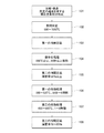
図1に本実施の形態に係る銅合金の製造工程フローの一例を示す。本実施の形態は、前述した銅合金組成を有する鋳塊を、圧延工程と熱処理工程とを組み合わせて所望の板厚まで加工する電気・電子部品用銅合金の製造方法において、前記熱処理工程では、次のように規定範囲内に設定された熱処理条件で熱処理をする。500℃以上550℃以下の温度で、30分以上6時間以下の時間で熱処理し、その後、更に400℃以上480℃以下の温度で、1時間以上10時間以下の熱処理をする。
(Manufacturing method of copper alloy for electric / electronic parts)
FIG. 1 shows an example of a manufacturing process flow of a copper alloy according to the present embodiment. The present embodiment is a method of manufacturing a copper alloy for electrical / electronic parts, in which the ingot having the above-described copper alloy composition is processed to a desired plate thickness by combining a rolling process and a heat treatment process. Heat treatment is performed under the heat treatment conditions set within the specified range as follows. Heat treatment is performed at a temperature of 500 ° C. or more and 550 ° C. or less for 30 minutes or more and 6 hours or less, and then, a heat treatment is further performed at a temperature of 400 ° C. or more and 480 ° C. or less for 1 hour or more and 10 hours or less.
以下、図1を用いて、銅合金の製造工程を工程ごとに詳述する。 Hereafter, the manufacturing process of a copper alloy is explained in full detail for every process using FIG.
(1)熱間圧延、第一の冷間圧延(ステップ102、103)
本実施の形態では前記銅合金を所定の温度によって熱間圧延する。熱間圧延は所定温度の炉にて800℃以上1050℃以下の温度に前記銅合金を保温した後、室温で圧延する。圧延の際中、若しくは圧延後常温に放置して室温まで冷却する。800℃未満であるとFeの析出量が多く、熱間圧延時に割れが起こりやすい。次に、第一の冷間圧延をする。第一の冷間圧延では加工熱が加わるが、外部からの加熱、冷却はなく、室温で圧延加工され、加工後は常温中にて保管される(後述する第二、第三の冷間圧延も同じ)。第一の冷間圧延に続く溶体化処理時において素材全体に均等に効率よく熱を伝えるためには、板厚を3mm以下になるように減面率を設定することが好ましい。
(1) Hot rolling, first cold rolling (
In the present embodiment, the copper alloy is hot-rolled at a predetermined temperature. In hot rolling, the copper alloy is kept at a temperature of 800 ° C. or higher and 1050 ° C. or lower in a furnace at a predetermined temperature, and then rolled at room temperature. Allow to cool to room temperature during rolling or after rolling. When the temperature is less than 800 ° C., the amount of Fe deposited is large, and cracking is likely to occur during hot rolling. Next, the first cold rolling is performed. In the first cold rolling, processing heat is applied, but there is no external heating and cooling, rolling is performed at room temperature, and after processing is stored at room temperature (second and third cold rolling described later) The same). In order to transmit heat uniformly and efficiently to the entire material during the solution treatment following the first cold rolling, it is preferable to set the area reduction rate so that the plate thickness is 3 mm or less.
(2)溶体化処理(ステップ104)
前記熱間圧延、冷間圧延後、900℃以上の温度で急激に加熱し30秒以上保持した後、直ちに500℃まで毎分100℃以上の冷却速度で冷却し、更に常温で室温まで自然冷却する。溶体化処理は熱間圧延時に析出した析出物を再固溶させるために行うものである。溶体化でFeを固溶(原子レベル(サブナノオーダー)の混合)状態から時効工程で析出(ナノオーダー)させる。しかし、数ナノオーダーのFe析出物は加工される(Cu母相の結晶粒界が通過する)と吸収されて再び固溶状態になる。これが再固溶状態である。固溶状態は析出状態よりも回復・再結晶抑制効果が小さく好ましくないと考えられる。この溶本化処理工程を省略すると目標とする強度および耐熱性が得られない。
(2) Solution treatment (step 104)
After the hot rolling and cold rolling, after rapidly heating at a temperature of 900 ° C. or higher and holding for 30 seconds or more, immediately cool to 500 ° C. at a cooling rate of 100 ° C. or more per minute, and further naturally cool to room temperature at room temperature. To do. The solution treatment is performed in order to re-dissolve the precipitate deposited during hot rolling. Fe is precipitated (nano-order) in the aging process from a solid solution (atomic level (sub-nano-order) mixed) state by solution treatment. However, several nano-order Fe precipitates are absorbed when processed (the crystal grain boundary of the Cu parent phase passes) and become a solid solution state again. This is a re-solution state. It is considered that the solid solution state is less preferable than the precipitated state because the effect of suppressing recovery and recrystallization is small. If this melt treatment step is omitted, the target strength and heat resistance cannot be obtained.
(3)第二の冷間圧延(ステップ105)
前記溶体化処理後、冷間圧延を行う。冷間圧延は減面率が50%以上となるように行うことが好ましい。これにより次に述べる時効での析出をスムーズにすることができる。
(3) Second cold rolling (step 105)
After the solution treatment, cold rolling is performed. It is preferable to perform the cold rolling so that the area reduction rate is 50% or more. Thereby, precipitation at the aging described below can be made smooth.
(4)第一の時効処理(ステップ106)
本実施の形態では時効を2回に分けて行う。1回の時効のみでは耐熱性が不十分となる。1回目の時効は500℃以上550℃以下の温度で、30分以上6時間以下の時間、好ましくは500℃以上530℃以下の温度で、2時間以上6時間以下の時間で熱処理を行う。熱処理後は徐々に冷却する。冷却は常温における冷却よりもゆっくりである(第二の時効も同じ)。時効温度は500℃未満ではFeを含有する粒子を十分に析出させることができず、目標とする強度および耐熱性を得られない。一方、550℃を越えるとコイル状に巻きつけている素材同士が粘着するという問題が生じる。また、時効時間が30分未満でも6時間を越えても、前記と同様の理由から目標とする耐熱性及び強度を得られない。
(4) First aging treatment (step 106)
In this embodiment, aging is performed in two steps. Heat resistance is insufficient with only one aging. The first aging is performed at a temperature of 500 ° C. to 550 ° C. for 30 minutes to 6 hours, preferably 500 ° C. to 530 ° C. for 2 hours to 6 hours. Cool gradually after heat treatment. Cooling is slower than cooling at room temperature (second aging is the same). If the aging temperature is less than 500 ° C., particles containing Fe cannot be sufficiently precipitated, and the target strength and heat resistance cannot be obtained. On the other hand, when the temperature exceeds 550 ° C., there arises a problem that the materials wound in the coil shape stick to each other. Further, even if the aging time is less than 30 minutes or exceeds 6 hours, the target heat resistance and strength cannot be obtained for the same reason as described above.
上述した素材同士の粘着とは、Feを速やかに析出させるために温度を高くし過ぎると、コイル状に巻かれた素材同士が意図せず拡散接合することである。ここでは、素材同士が粘着しないように条件を設定している点が重要である。素材同士の粘着は素材をコイル状に巻いて熱処理をする工程において問題となる点であり、この間題は高温になるほど顕著になる。そのため、粘着が生じない範囲内の時効温度から耐熱性を維持するために必要な第一の形態の銅合金を得られる条件としている。 The adhesion between the materials described above means that the materials wound in a coil shape are diffusion-bonded unintentionally when the temperature is too high in order to rapidly precipitate Fe. Here, it is important that the conditions are set so that the materials do not stick to each other. Adhesion between materials is a problem in a process of winding a material in a coil shape and performing a heat treatment, and this problem becomes more prominent as the temperature becomes higher. Therefore, it is set as the conditions which can obtain the copper alloy of the 1st form required in order to maintain heat resistance from the aging temperature in the range which does not produce adhesion.
(5)第二の時効処理(ステップ107)
2回目の時効を400℃以上480℃以下の温度で、1時間以上8時間以下の時間、好ましくは400℃以上450℃以下の温度で、2時間以上6時間以下の時間で熱処理を行う。400℃よりも低い温度では析出に長時間を要し、480℃より高い温度では目標とする耐熱性が得られない。なお、第一の時効と第二の時効は連続して行うので、温度履歴は第一の時効温度まで昇温、第一の時効温度で保持、第二の時効温度まで降温、第二の時効温度で保持、常温まで冷却としている。
(5) Second aging process (step 107)
The second aging is performed at a temperature of 400 ° C. to 480 ° C. for 1 hour to 8 hours, preferably at a temperature of 400 ° C. to 450 ° C. for 2 hours to 6 hours. Precipitation takes a long time at temperatures lower than 400 ° C., and target heat resistance cannot be obtained at temperatures higher than 480 ° C. Since the first aging and the second aging are performed continuously, the temperature history is raised to the first aging temperature, held at the first aging temperature, lowered to the second aging temperature, and the second aging. Hold at temperature and cool to room temperature.
(6)第三の冷間圧延(ステップ108)
前記時効後、仕上圧延を加工度70%以上85%以下で冷間にて行う。これにより目標の強度を得ることができる。なお、更にこの後に、伸びの向上や歪除去のために低温焼鈍を行っても良い。
(6) Third cold rolling (step 108)
After the aging, finish rolling is performed cold at a working degree of 70% to 85%. Thereby, the target intensity can be obtained. Further, after this, low-temperature annealing may be performed to improve elongation and remove strain.
(電気・電子部品用銅合金の製造方法の実施の形態に係る効果)
第一の実施の形態の鋳塊を、圧延工程と熱処理工程とを組み合わせて所望の板厚まで加工する電気・電子部品用銅合金の製造方法において、前記熱処理工程では、500℃以上550℃以下の温度で、30分以上6時間以下の時間で熱処理をし、その後、更に400℃以上480℃以下の温度で、1時間以上8時間以下の時間で熱処理をすることにより、銅母相中に分散するFeを含有する粒子の中で、直径が50nmより大きい粒子の数密度N1と、直径が50nm以下である粒子の数密度N2との比N2/N1が5以上であり、直径が20nm以上50nm以下の粒子における平均粒子間隔が50nm以上300nm以下である銅合金を実現できる。特に、時効温度を550℃以下としたので、素材をコイル状に巻いて熱処理をする工程において問題となる素材同士の粘着を生じないようにすることができる。したがって、素材同士の粘着を生じることなく、耐熱性に優れた電気・電子部品用銅合金を製造できる。
(Effects of Embodiment of Manufacturing Method of Copper Alloy for Electric / Electronic Parts)
In the method of manufacturing a copper alloy for electric / electronic parts, which is a combination of a rolling process and a heat treatment process, and the ingot of the first embodiment is processed to a desired plate thickness, Heat treatment at a temperature of 30 minutes to 6 hours and then heat treatment at a temperature of 400 ° C. to 480 ° C. for a time of 1 hour to 8 hours. Among the particles containing Fe to be dispersed, the ratio N 2 / N 1 of the number density N 1 of particles having a diameter larger than 50 nm and the number density N 2 of particles having a diameter of 50 nm or less is 5 or more, A copper alloy having an average particle interval of 50 nm to 300 nm in particles having a diameter of 20 nm to 50 nm can be realized. In particular, since the aging temperature is set to 550 ° C. or lower, it is possible to prevent the materials from sticking to each other which becomes a problem in the process of winding the materials in a coil shape and performing the heat treatment. Therefore, it is possible to produce a copper alloy for electric / electronic parts having excellent heat resistance without causing adhesion between materials.
なお、時効処理回数は2回に限定されるものではなく3回以上行ってもよい。その場合、各事項条件は回数に合わせて適切に設定される。 Note that the number of aging treatments is not limited to two, but may be three or more. In that case, each item condition is appropriately set according to the number of times.
以下、本発明を実施例に基づいてさらに詳しく説明するが、本発明はこれらに限定されるものではない。 EXAMPLES Hereinafter, although this invention is demonstrated in more detail based on an Example, this invention is not limited to these.
(実施例1)
重量%にして2.2%のFe、0.03%のP、0.0l%のZnを含有し、残部がCuと不可避不純物からなる銅合金を高周波誘導型坩堝で溶解後、銅製鋳型で半連続鋳造し、横断面200mm×450mm、長さ4000mmの直方体の鋳塊を作製した。
Example 1
A copper alloy containing 2.2% Fe, 0.03% P, and 0.01% Zn, with the balance being Cu and inevitable impurities, is melted in a high-frequency induction crucible, and then a copper mold. Semi-continuous casting was performed to produce a rectangular ingot having a cross section of 200 mm × 450 mm and a length of 4000 mm.
この鋳塊の表面をそれぞれ5mm面削し、950℃で2時間保持後熱間圧延を行い、板厚12mmとした。更に表面および裏面をそれぞれ1mm面削した後、第一冷間圧延により板厚2.5mmとした。 The surface of each ingot was chamfered by 5 mm, held at 950 ° C. for 2 hours, and then hot-rolled to a plate thickness of 12 mm. Further, the front surface and the back surface were each cut by 1 mm, and then the plate thickness was adjusted to 2.5 mm by first cold rolling.
次に、材料の最高温度が最大925℃になるように制御しながら、連続焼鈍炉の加熱帯中に材料を走行させた。加熱帯に続いて、冷却帯および水冷プールを通過させて急冷させて溶体化処理とした。 Next, the material was run through the heating zone of the continuous annealing furnace while controlling the maximum temperature of the material to be 925 ° C. at the maximum. Subsequent to the heating zone, the solution was quenched by passing through a cooling zone and a water-cooled pool.
更に表面及び裏面を研磨した後、第二冷間圧延により板厚0.7mmとした。 Furthermore, after grind | polishing the surface and the back surface, it was set as plate | board thickness 0.7mm by the 2nd cold rolling.
次に電気炉を用いて窒素ガス雰囲気中で550℃の温度で4時間焼鈍し、冷却速度5℃/分で450℃まで降温した。450℃まで到達後2時間焼鈍し、冷却速度毎分5℃/分の冷却速度で室温に下げた。 Next, annealing was performed for 4 hours at a temperature of 550 ° C. in a nitrogen gas atmosphere using an electric furnace, and the temperature was lowered to 450 ° C. at a cooling rate of 5 ° C./min. After reaching 450 ° C., annealing was performed for 2 hours, and the temperature was lowered to room temperature at a cooling rate of 5 ° C./min.
次に、第三冷間圧延により板厚0.25mmとした。 Next, the plate thickness was set to 0.25 mm by third cold rolling.
このときのFeを含有する粒子および特性を評価した。
Fe粒子を含有する粒子の析出物のサイズ分布、体積率はX線小角散乱法を用いて評価した。X線小角散乱法による測定結果の解析には球状のFe粒子を散乱体モデルとして評価した。なお、散乱体モデルをFeの球状粒子と仮定したのは、透過電子顕微鏡を用いて分散相を、2次元で観察した結果、大多数はFeを多量に含有する円状粒子であったためである。すなわち、断面の方向によらず、円状であったため、3次元では、球状粒子であると考えられるためである。
At this time, Fe-containing particles and properties were evaluated.
The size distribution and volume ratio of precipitates of particles containing Fe particles were evaluated using the X-ray small angle scattering method. For analysis of the measurement results by the X-ray small angle scattering method, spherical Fe particles were evaluated as a scatterer model. The reason why the scatterer model is assumed to be a spherical particle of Fe is that, as a result of observing the dispersed phase in two dimensions using a transmission electron microscope, the majority were circular particles containing a large amount of Fe. . That is, because it is circular regardless of the direction of the cross section, it is considered to be a spherical particle in three dimensions.
平均粒子間隔は、小角散乱法による粒子の解析結果を用いて、図2に示す平均粒子間隔の算出モデルを参照しつつ、以下のように導出した。f、dはX線小角散乱法にて測定・解析したFeを含有する直径20nm以上50nm以下の粒子1における(母相に対する)体積率および粒子直径の最大値である。
体積率fは、
f={(4/3)・π・(d/2)3}/x3 ・・・(1)
xは、
x=l+d ・・・(2)
式(1)及び式(2)より、平均粒子間隔lを求めると次のようになる。
l={(π/6f)1/3−1}・d ・・・(3)
The average particle interval was derived as follows using the analysis result of the particles by the small angle scattering method and referring to the calculation model of the average particle interval shown in FIG. f and d are the volume ratio (relative to the parent phase) and the maximum value of the particle diameter in the particle 1 containing 20 to 50 nm in diameter containing and measured and analyzed by the X-ray small angle scattering method.
The volume ratio f is
f = {(4/3) · π · (d / 2) 3 } / x 3 (1)
x is
x = l + d (2)
From the equations (1) and (2), the average particle spacing l is obtained as follows.
l = {(π / 6f) 1/3 −1} · d (3)
引張強さは引張強さ、0.2%耐力、伸びはJIS Z2241に準拠した引張試験で測定し、導電率はシグマテスタ(渦電流を利用したIACS%測定器)を用いて評価した。また、耐熱性の評価として、熱処理前後のビッカース硬さを以下の方法で評価した。すなわち、仕上圧延後のビッカース硬さとリードフレームに加工した後に処理される歪除去の熱処理を模擬した450℃×5分の熱処理後のビッカース硬さの差(変化)で評価した
。20Hv以下が許容される範囲である。
Tensile strength was measured by tensile strength, 0.2% proof stress, and elongation was measured by a tensile test in accordance with JIS Z2241, and conductivity was evaluated using a sigma tester (IACS% measuring instrument using eddy current). Further, as an evaluation of heat resistance, Vickers hardness before and after heat treatment was evaluated by the following method. That is, the difference (change) between the Vickers hardness after the finish rolling and the Vickers hardness after the heat treatment of 450 ° C. × 5 minutes simulating the heat treatment for removing the strain processed after processing into the lead frame was evaluated. 20Hv or less is an allowable range.
評価結果を表1に示す。表1は、本発明の実施例及び比較例における時効条件、N2/NI比、平均粒子間隔、引張強さ、導電率、熱処理前後のビッカー硬さの変化を示したものある。

(実施例2〜3〉
実施例2〜3は表1に示した時効処理条件を除いて実施例1と同様に製造した。時効処理条件を規定範囲内に設定した実施例2〜3では、実施例1と同様に良好な特性が得られた。
(Examples 2-3)
Examples 2 to 3 were produced in the same manner as Example 1 except for the aging treatment conditions shown in Table 1. In Examples 2 to 3 in which the aging treatment conditions were set within the specified range, good characteristics were obtained as in Example 1.
(比較例1〜4)
比較例1〜4も表1に示した時効処理条件を除いて実施例1と同様に製造した。第一の時効時間を8時間と規定範囲外に設定した比較例1、第一の時効温度を480℃、第一の時効時間を10時間と2つの条件をともに規定範囲外に設定した比較例2、及び第二の時効温度を380℃、第二の時効時間を10時間と2つの条件をともに規定範囲外に設定した比較例3では、N2/N1比または/および平均粒子間隔が規定範囲からはずれ、熱処理後のビッカース硬さの低下が規定範囲を超えた。また、第一の時効温度を600℃と規定範囲外に設定した比較例4では、N2/N1比、平均粒子間隔、引張強さ、導電率、熱処理前後のビッカース硬さの変化はいずれも良好な特性が得られたものの、コイル状に巻かれた素材同士に粘着が生じていた。
(Comparative Examples 1-4)
Comparative Examples 1 to 4 were also produced in the same manner as Example 1 except for the aging treatment conditions shown in Table 1. Comparative Example 1 in which the first aging time was set to 8 hours outside the specified range, Comparative Example in which the first aging temperature was set to 480 ° C., the first aging time was set to 10 hours, and both conditions were set outside the specified range. 2 and the second aging temperature was 380 ° C., the second aging time was 10 hours, and both of the two conditions were set outside the specified range, the N 2 / N 1 ratio or / and the average particle spacing were Deviating from the specified range, the decrease in Vickers hardness after heat treatment exceeded the specified range. Further, in Comparative Example 4 in which the first aging temperature was set to 600 ° C. and out of the specified range, N 2 / N 1 ratio, average particle spacing, tensile strength, conductivity, and changes in Vickers hardness before and after heat treatment Although good characteristics were obtained, adhesion was generated between the materials wound in a coil shape.
1 Feを含有する粒子 1 Fe-containing particles
Claims (4)
銅母相中に分散するFeを含有する粒子の中で、直径が50nmより大きい粒子の数密度N1と、直径が50nm以下である粒子の数密度N2との比N2/N1が5以上8以下であり、
X線小角散乱法にて測定・解析したFeを含有する直径20nm以上50nm以下の粒子における、母相に対する体積率fおよび粒子直径の最大値dを用いて式(3)で求められる、直径が20nm以上50nm以下の粒子における平均粒子間隔lが50nm以上300nm以下である電気・電子部品用銅合金。
l=[{π/(6f)} 1/3 −1]・d 式(3) Fe containing 2.0 wt% or more and 2.6 wt% or less, P containing 0.01 wt% or more and 0.2 wt% or less, Zn containing 0.01 wt% or more and 1.0 wt% or less, with the balance being Cu In copper alloys for electrical and electronic parts consisting of inevitable impurities
Among the particles containing Fe dispersed in the copper matrix, the ratio N 2 / N 1 of the number density N 1 of particles having a diameter larger than 50 nm and the number density N 2 of particles having a diameter of 50 nm or less is 5 or more and 8 or less ,
The diameter determined by the equation (3) using the volume fraction f with respect to the parent phase and the maximum value d of the particle diameter in particles containing 20 to 50 nm in diameter and containing Fe measured and analyzed by the X-ray small angle scattering method is A copper alloy for electrical / electronic parts, wherein an average particle spacing l of particles of 20 nm to 50 nm is 50 nm to 300 nm.
l = [{π / (6f)} 1/3 −1] · d Formula (3)
前記第二の時効処理では、400℃以上450℃以下の温度で、2時間以上6時間以下の時間で熱処理をする請求項3に記載の電気・電子部品用銅合金の製造方法。 In the first aging treatment, heat treatment is performed at a temperature of 500 ° C. or more and 530 ° C. or less for 2 hours or more and 6 hours or less,
The method for producing a copper alloy for electrical / electronic parts according to claim 3, wherein in the second aging treatment, heat treatment is performed at a temperature of 400 ° C or higher and 450 ° C or lower for a time of 2 hours or longer and 6 hours or shorter.
Priority Applications (1)
| Application Number | Priority Date | Filing Date | Title |
|---|---|---|---|
| JP2010257995A JP5638357B2 (en) | 2010-11-18 | 2010-11-18 | Copper alloy for electrical and electronic parts and method for producing the same |
Applications Claiming Priority (1)
| Application Number | Priority Date | Filing Date | Title |
|---|---|---|---|
| JP2010257995A JP5638357B2 (en) | 2010-11-18 | 2010-11-18 | Copper alloy for electrical and electronic parts and method for producing the same |
Publications (2)
| Publication Number | Publication Date |
|---|---|
| JP2012107297A JP2012107297A (en) | 2012-06-07 |
| JP5638357B2 true JP5638357B2 (en) | 2014-12-10 |
Family
ID=46493202
Family Applications (1)
| Application Number | Title | Priority Date | Filing Date |
|---|---|---|---|
| JP2010257995A Active JP5638357B2 (en) | 2010-11-18 | 2010-11-18 | Copper alloy for electrical and electronic parts and method for producing the same |
Country Status (1)
| Country | Link |
|---|---|
| JP (1) | JP5638357B2 (en) |
Families Citing this family (3)
| Publication number | Priority date | Publication date | Assignee | Title |
|---|---|---|---|---|
| WO2013002272A1 (en) * | 2011-06-30 | 2013-01-03 | 大電株式会社 | Flexible conductive material, and cable using same |
| JP6210887B2 (en) * | 2014-01-18 | 2017-10-11 | 株式会社神戸製鋼所 | Fe-P copper alloy sheet with excellent strength, heat resistance and bending workability |
| CN113088750B (en) * | 2021-03-19 | 2022-03-25 | 宁波金田铜业(集团)股份有限公司 | Copper-iron alloy wire and preparation method thereof |
Family Cites Families (6)
| Publication number | Priority date | Publication date | Assignee | Title |
|---|---|---|---|---|
| JPH1180862A (en) * | 1997-09-09 | 1999-03-26 | Kobe Steel Ltd | Copper-iron alloy material for lead frame, excellent in heat resistance |
| JP3763234B2 (en) * | 1999-08-05 | 2006-04-05 | 日立電線株式会社 | Method for producing high-strength, high-conductivity, high-heat-resistant copper-based alloy |
| JP3896793B2 (en) * | 2001-02-16 | 2007-03-22 | 日立電線株式会社 | Manufacturing method of high strength and high conductivity copper alloy material |
| JP3798260B2 (en) * | 2001-05-17 | 2006-07-19 | 株式会社神戸製鋼所 | Copper alloy for electric and electronic parts and electric and electronic parts |
| JP3766051B2 (en) * | 2002-09-03 | 2006-04-12 | 株式会社神戸製鋼所 | Copper alloy having excellent heat resistance and method for producing the same |
| JP5570109B2 (en) * | 2008-10-15 | 2014-08-13 | 三菱伸銅株式会社 | Copper alloy and lead frame material for electronic equipment |
-
2010
- 2010-11-18 JP JP2010257995A patent/JP5638357B2/en active Active
Also Published As
| Publication number | Publication date |
|---|---|
| JP2012107297A (en) | 2012-06-07 |
Similar Documents
| Publication | Publication Date | Title |
|---|---|---|
| JP5312920B2 (en) | Copper alloy plate or strip for electronic materials | |
| JP4677505B1 (en) | Cu-Ni-Si-Co-based copper alloy for electronic materials and method for producing the same | |
| JP5647703B2 (en) | High-strength Cu-Ni-Co-Si-based copper alloy sheet, its manufacturing method, and current-carrying parts | |
| JP5441876B2 (en) | Cu-Ni-Si-Co-based copper alloy for electronic materials and method for producing the same | |
| TWI422692B (en) | Cu-Co-Si based copper alloy for electronic materials and method for producing the same | |
| JP5140045B2 (en) | Cu-Ni-Si alloy plate or strip for electronic materials | |
| TWI429768B (en) | Cu-Co-Si based copper alloy for electronic materials and method for producing the same | |
| JP2008248333A (en) | Cu-Ni-Si-Co-BASED COPPER ALLOY FOR ELECTRONIC MATERIAL, AND MANUFACTURING METHOD THEREFOR | |
| JP5451674B2 (en) | Cu-Si-Co based copper alloy for electronic materials and method for producing the same | |
| JP6222885B2 (en) | Cu-Ni-Si-Co based copper alloy for electronic materials | |
| JP5555154B2 (en) | Copper alloy for electrical and electronic parts and method for producing the same | |
| JP5638357B2 (en) | Copper alloy for electrical and electronic parts and method for producing the same | |
| JP6730784B2 (en) | Cu-Ni-Co-Si alloy for electronic parts | |
| JP6821290B2 (en) | Cu-Ni-Co-Si alloy for electronic components | |
| JP5988794B2 (en) | Copper alloy sheet and manufacturing method thereof | |
| JP5524901B2 (en) | Cu-Ni-Si-Co based copper alloy for electronic materials | |
| US10358697B2 (en) | Cu—Co—Ni—Si alloy for electronic components | |
| JP2011246740A (en) | Cu-Co-Si BASED ALLOY SHEET OR STRIP FOR ELECTRONIC MATERIAL | |
| JP2012229467A (en) | Cu-Ni-Si BASED COPPER ALLOY FOR ELECTRONIC MATERIAL | |
| JP2011046970A (en) | Copper alloy material and method for producing the same | |
| JP2016211053A (en) | Copper alloy excellent in heat resistance | |
| JP6246174B2 (en) | Cu-Co-Ni-Si alloy for electronic parts | |
| JP2018204115A (en) | Copper alloy having excellent heat resistance | |
| JP6830135B2 (en) | Cu-Ni-Co-Si alloy for electronic components | |
| JPWO2018235458A1 (en) | Copper alloy ultrafine wire for spring and method for producing the same |
Legal Events
| Date | Code | Title | Description |
|---|---|---|---|
| A621 | Written request for application examination |
Free format text: JAPANESE INTERMEDIATE CODE: A621 Effective date: 20130125 |
|
| A711 | Notification of change in applicant |
Free format text: JAPANESE INTERMEDIATE CODE: A712 Effective date: 20130628 |
|
| RD04 | Notification of resignation of power of attorney |
Free format text: JAPANESE INTERMEDIATE CODE: A7424 Effective date: 20131016 |
|
| A131 | Notification of reasons for refusal |
Free format text: JAPANESE INTERMEDIATE CODE: A131 Effective date: 20140311 |
|
| A521 | Written amendment |
Free format text: JAPANESE INTERMEDIATE CODE: A523 Effective date: 20140502 |
|
| A131 | Notification of reasons for refusal |
Free format text: JAPANESE INTERMEDIATE CODE: A131 Effective date: 20140610 |
|
| A521 | Written amendment |
Free format text: JAPANESE INTERMEDIATE CODE: A523 Effective date: 20140620 |
|
| TRDD | Decision of grant or rejection written | ||
| A01 | Written decision to grant a patent or to grant a registration (utility model) |
Free format text: JAPANESE INTERMEDIATE CODE: A01 Effective date: 20141007 |
|
| A61 | First payment of annual fees (during grant procedure) |
Free format text: JAPANESE INTERMEDIATE CODE: A61 Effective date: 20141022 |
|
| R150 | Certificate of patent or registration of utility model |
Ref document number: 5638357 Country of ref document: JP Free format text: JAPANESE INTERMEDIATE CODE: R150 |