JP5631497B1 - Semiconductor junction protecting glass composition, semiconductor device manufacturing method, and semiconductor device - Google Patents
Semiconductor junction protecting glass composition, semiconductor device manufacturing method, and semiconductor device Download PDFInfo
- Publication number
- JP5631497B1 JP5631497B1 JP2013530477A JP2013530477A JP5631497B1 JP 5631497 B1 JP5631497 B1 JP 5631497B1 JP 2013530477 A JP2013530477 A JP 2013530477A JP 2013530477 A JP2013530477 A JP 2013530477A JP 5631497 B1 JP5631497 B1 JP 5631497B1
- Authority
- JP
- Japan
- Prior art keywords
- semiconductor
- glass
- junction
- glass composition
- protecting
- Prior art date
- Legal status (The legal status is an assumption and is not a legal conclusion. Google has not performed a legal analysis and makes no representation as to the accuracy of the status listed.)
- Active
Links
- 239000004065 semiconductor Substances 0.000 title claims abstract description 618
- 239000011521 glass Substances 0.000 title claims abstract description 439
- 239000000203 mixture Substances 0.000 title claims abstract description 242
- 238000004519 manufacturing process Methods 0.000 title claims abstract description 113
- 239000002994 raw material Substances 0.000 claims abstract description 29
- 229910000287 alkaline earth metal oxide Inorganic materials 0.000 claims abstract description 25
- 229910052785 arsenic Inorganic materials 0.000 claims abstract description 17
- 229910052787 antimony Inorganic materials 0.000 claims abstract description 15
- 239000000945 filler Substances 0.000 claims abstract description 15
- 229910052745 lead Inorganic materials 0.000 claims abstract description 15
- 229910052744 lithium Inorganic materials 0.000 claims abstract description 15
- 239000000155 melt Substances 0.000 claims abstract description 15
- 229910052700 potassium Inorganic materials 0.000 claims abstract description 14
- 229910052708 sodium Inorganic materials 0.000 claims abstract description 14
- 238000002844 melting Methods 0.000 claims abstract description 13
- 230000008018 melting Effects 0.000 claims abstract description 13
- 239000010419 fine particle Substances 0.000 claims abstract description 11
- 229910004298 SiO 2 Inorganic materials 0.000 claims description 35
- 229910018072 Al 2 O 3 Inorganic materials 0.000 claims description 33
- 238000011084 recovery Methods 0.000 claims description 23
- 229910000480 nickel oxide Inorganic materials 0.000 claims description 19
- GNRSAWUEBMWBQH-UHFFFAOYSA-N oxonickel Chemical compound [Ni]=O GNRSAWUEBMWBQH-UHFFFAOYSA-N 0.000 claims description 19
- -1 B 2 O 3 Inorganic materials 0.000 claims description 18
- 230000009477 glass transition Effects 0.000 claims description 9
- 229910052784 alkaline earth metal Inorganic materials 0.000 claims description 8
- 150000001342 alkaline earth metals Chemical class 0.000 claims description 8
- 238000010304 firing Methods 0.000 abstract description 33
- 239000000463 material Substances 0.000 abstract description 31
- XLOMVQKBTHCTTD-UHFFFAOYSA-N zinc oxide Inorganic materials [Zn]=O XLOMVQKBTHCTTD-UHFFFAOYSA-N 0.000 abstract description 29
- BPQQTUXANYXVAA-UHFFFAOYSA-N Orthosilicate Chemical compound [O-][Si]([O-])([O-])[O-] BPQQTUXANYXVAA-UHFFFAOYSA-N 0.000 abstract description 15
- VYPSYNLAJGMNEJ-UHFFFAOYSA-N Silicium dioxide Chemical compound O=[Si]=O VYPSYNLAJGMNEJ-UHFFFAOYSA-N 0.000 abstract description 6
- 229910011255 B2O3 Inorganic materials 0.000 abstract 1
- PNEYBMLMFCGWSK-UHFFFAOYSA-N aluminium oxide Inorganic materials [O-2].[O-2].[O-2].[Al+3].[Al+3] PNEYBMLMFCGWSK-UHFFFAOYSA-N 0.000 abstract 1
- QVQLCTNNEUAWMS-UHFFFAOYSA-N barium oxide Inorganic materials [Ba]=O QVQLCTNNEUAWMS-UHFFFAOYSA-N 0.000 abstract 1
- 229910052681 coesite Inorganic materials 0.000 abstract 1
- 229910052593 corundum Inorganic materials 0.000 abstract 1
- 229910052906 cristobalite Inorganic materials 0.000 abstract 1
- 239000000377 silicon dioxide Substances 0.000 abstract 1
- 235000012239 silicon dioxide Nutrition 0.000 abstract 1
- 229910052682 stishovite Inorganic materials 0.000 abstract 1
- 229910052905 tridymite Inorganic materials 0.000 abstract 1
- 229910001845 yogo sapphire Inorganic materials 0.000 abstract 1
- 239000000758 substrate Substances 0.000 description 123
- 238000000034 method Methods 0.000 description 81
- 238000011156 evaluation Methods 0.000 description 69
- 229910001385 heavy metal Inorganic materials 0.000 description 34
- 230000015572 biosynthetic process Effects 0.000 description 33
- 238000009792 diffusion process Methods 0.000 description 33
- 230000001681 protective effect Effects 0.000 description 25
- PXHVJJICTQNCMI-UHFFFAOYSA-N nickel Substances [Ni] PXHVJJICTQNCMI-UHFFFAOYSA-N 0.000 description 24
- 230000008569 process Effects 0.000 description 24
- 239000012535 impurity Substances 0.000 description 20
- 238000007747 plating Methods 0.000 description 17
- BASFCYQUMIYNBI-UHFFFAOYSA-N platinum Substances [Pt] BASFCYQUMIYNBI-UHFFFAOYSA-N 0.000 description 16
- 238000005520 cutting process Methods 0.000 description 14
- HBMJWWWQQXIZIP-UHFFFAOYSA-N silicon carbide Chemical group [Si+]#[C-] HBMJWWWQQXIZIP-UHFFFAOYSA-N 0.000 description 12
- 229910010271 silicon carbide Inorganic materials 0.000 description 12
- 230000006798 recombination Effects 0.000 description 11
- XUIMIQQOPSSXEZ-UHFFFAOYSA-N Silicon Chemical compound [Si] XUIMIQQOPSSXEZ-UHFFFAOYSA-N 0.000 description 10
- 238000002161 passivation Methods 0.000 description 10
- 229910052710 silicon Inorganic materials 0.000 description 10
- 239000010703 silicon Substances 0.000 description 10
- 230000000052 comparative effect Effects 0.000 description 9
- 239000000126 substance Substances 0.000 description 9
- 238000001962 electrophoresis Methods 0.000 description 8
- 238000005530 etching Methods 0.000 description 8
- 238000005215 recombination Methods 0.000 description 8
- 230000004888 barrier function Effects 0.000 description 7
- 238000010586 diagram Methods 0.000 description 7
- 229910052782 aluminium Inorganic materials 0.000 description 6
- 238000007796 conventional method Methods 0.000 description 6
- 238000002425 crystallisation Methods 0.000 description 6
- 230000008025 crystallization Effects 0.000 description 6
- 230000000694 effects Effects 0.000 description 6
- 229910052751 metal Inorganic materials 0.000 description 6
- 239000002184 metal Substances 0.000 description 6
- 239000002245 particle Substances 0.000 description 6
- 238000002360 preparation method Methods 0.000 description 6
- 239000002585 base Substances 0.000 description 5
- 238000005304 joining Methods 0.000 description 5
- 230000003647 oxidation Effects 0.000 description 5
- 238000007254 oxidation reaction Methods 0.000 description 5
- 238000004017 vitrification Methods 0.000 description 5
- IJGRMHOSHXDMSA-UHFFFAOYSA-N Atomic nitrogen Chemical compound N#N IJGRMHOSHXDMSA-UHFFFAOYSA-N 0.000 description 4
- MCMNRKCIXSYSNV-UHFFFAOYSA-N Zirconium dioxide Chemical compound O=[Zr]=O MCMNRKCIXSYSNV-UHFFFAOYSA-N 0.000 description 4
- 238000000137 annealing Methods 0.000 description 4
- 239000011230 binding agent Substances 0.000 description 4
- 239000000969 carrier Substances 0.000 description 4
- 238000002156 mixing Methods 0.000 description 4
- 229910052697 platinum Inorganic materials 0.000 description 4
- 229910052814 silicon oxide Inorganic materials 0.000 description 4
- 238000004544 sputter deposition Methods 0.000 description 4
- QZPSXPBJTPJTSZ-UHFFFAOYSA-N aqua regia Chemical compound Cl.O[N+]([O-])=O QZPSXPBJTPJTSZ-UHFFFAOYSA-N 0.000 description 3
- 238000007606 doctor blade method Methods 0.000 description 3
- 238000009413 insulation Methods 0.000 description 3
- 229910052759 nickel Inorganic materials 0.000 description 3
- 238000001259 photo etching Methods 0.000 description 3
- 238000007650 screen-printing Methods 0.000 description 3
- 238000004528 spin coating Methods 0.000 description 3
- 238000003756 stirring Methods 0.000 description 3
- 238000007740 vapor deposition Methods 0.000 description 3
- 239000012808 vapor phase Substances 0.000 description 3
- RTAQQCXQSZGOHL-UHFFFAOYSA-N Titanium Chemical compound [Ti] RTAQQCXQSZGOHL-UHFFFAOYSA-N 0.000 description 2
- 230000004913 activation Effects 0.000 description 2
- QVGXLLKOCUKJST-UHFFFAOYSA-N atomic oxygen Chemical compound [O] QVGXLLKOCUKJST-UHFFFAOYSA-N 0.000 description 2
- 229910052796 boron Inorganic materials 0.000 description 2
- 230000000875 corresponding effect Effects 0.000 description 2
- 230000007613 environmental effect Effects 0.000 description 2
- AMWRITDGCCNYAT-UHFFFAOYSA-L hydroxy(oxo)manganese;manganese Chemical compound [Mn].O[Mn]=O.O[Mn]=O AMWRITDGCCNYAT-UHFFFAOYSA-L 0.000 description 2
- 229910052757 nitrogen Inorganic materials 0.000 description 2
- 239000001301 oxygen Substances 0.000 description 2
- 229910052760 oxygen Inorganic materials 0.000 description 2
- 229910052698 phosphorus Inorganic materials 0.000 description 2
- 239000010936 titanium Substances 0.000 description 2
- 229910052719 titanium Inorganic materials 0.000 description 2
- QPLDLSVMHZLSFG-UHFFFAOYSA-N Copper oxide Chemical compound [Cu]=O QPLDLSVMHZLSFG-UHFFFAOYSA-N 0.000 description 1
- 239000005751 Copper oxide Substances 0.000 description 1
- MYMOFIZGZYHOMD-UHFFFAOYSA-N Dioxygen Chemical compound O=O MYMOFIZGZYHOMD-UHFFFAOYSA-N 0.000 description 1
- BQCADISMDOOEFD-UHFFFAOYSA-N Silver Chemical compound [Ag] BQCADISMDOOEFD-UHFFFAOYSA-N 0.000 description 1
- 239000003513 alkali Substances 0.000 description 1
- XAGFODPZIPBFFR-UHFFFAOYSA-N aluminium Chemical compound [Al] XAGFODPZIPBFFR-UHFFFAOYSA-N 0.000 description 1
- 239000002518 antifoaming agent Substances 0.000 description 1
- 239000012298 atmosphere Substances 0.000 description 1
- 229910052797 bismuth Inorganic materials 0.000 description 1
- 238000004140 cleaning Methods 0.000 description 1
- 238000000576 coating method Methods 0.000 description 1
- 229910000431 copper oxide Inorganic materials 0.000 description 1
- 239000013078 crystal Substances 0.000 description 1
- 230000002542 deteriorative effect Effects 0.000 description 1
- 229910001882 dioxygen Inorganic materials 0.000 description 1
- 238000002474 experimental method Methods 0.000 description 1
- 239000006260 foam Substances 0.000 description 1
- 230000005484 gravity Effects 0.000 description 1
- 238000010438 heat treatment Methods 0.000 description 1
- 238000002513 implantation Methods 0.000 description 1
- 238000005468 ion implantation Methods 0.000 description 1
- 238000012986 modification Methods 0.000 description 1
- 230000004048 modification Effects 0.000 description 1
- 150000004767 nitrides Chemical class 0.000 description 1
- RVTZCBVAJQQJTK-UHFFFAOYSA-N oxygen(2-);zirconium(4+) Chemical compound [O-2].[O-2].[Zr+4] RVTZCBVAJQQJTK-UHFFFAOYSA-N 0.000 description 1
- 229910052709 silver Inorganic materials 0.000 description 1
- 239000004332 silver Substances 0.000 description 1
- 238000003892 spreading Methods 0.000 description 1
- 230000007480 spreading Effects 0.000 description 1
- 231100000331 toxic Toxicity 0.000 description 1
- 230000002588 toxic effect Effects 0.000 description 1
- 230000007704 transition Effects 0.000 description 1
- 229910001928 zirconium oxide Inorganic materials 0.000 description 1
Images


Classifications
-
- H—ELECTRICITY
- H01—ELECTRIC ELEMENTS
- H01L—SEMICONDUCTOR DEVICES NOT COVERED BY CLASS H10
- H01L21/00—Processes or apparatus adapted for the manufacture or treatment of semiconductor or solid state devices or of parts thereof
- H01L21/02—Manufacture or treatment of semiconductor devices or of parts thereof
- H01L21/02104—Forming layers
- H01L21/02107—Forming insulating materials on a substrate
- H01L21/02109—Forming insulating materials on a substrate characterised by the type of layer, e.g. type of material, porous/non-porous, pre-cursors, mixtures or laminates
- H01L21/02112—Forming insulating materials on a substrate characterised by the type of layer, e.g. type of material, porous/non-porous, pre-cursors, mixtures or laminates characterised by the material of the layer
- H01L21/02123—Forming insulating materials on a substrate characterised by the type of layer, e.g. type of material, porous/non-porous, pre-cursors, mixtures or laminates characterised by the material of the layer the material containing silicon
- H01L21/02142—Forming insulating materials on a substrate characterised by the type of layer, e.g. type of material, porous/non-porous, pre-cursors, mixtures or laminates characterised by the material of the layer the material containing silicon the material containing silicon and at least one metal element, e.g. metal silicate based insulators or metal silicon oxynitrides
-
- H—ELECTRICITY
- H01—ELECTRIC ELEMENTS
- H01L—SEMICONDUCTOR DEVICES NOT COVERED BY CLASS H10
- H01L23/00—Details of semiconductor or other solid state devices
- H01L23/28—Encapsulations, e.g. encapsulating layers, coatings, e.g. for protection
- H01L23/29—Encapsulations, e.g. encapsulating layers, coatings, e.g. for protection characterised by the material, e.g. carbon
- H01L23/291—Oxides or nitrides or carbides, e.g. ceramics, glass
-
- C—CHEMISTRY; METALLURGY
- C03—GLASS; MINERAL OR SLAG WOOL
- C03C—CHEMICAL COMPOSITION OF GLASSES, GLAZES OR VITREOUS ENAMELS; SURFACE TREATMENT OF GLASS; SURFACE TREATMENT OF FIBRES OR FILAMENTS MADE FROM GLASS, MINERALS OR SLAGS; JOINING GLASS TO GLASS OR OTHER MATERIALS
- C03C3/00—Glass compositions
- C03C3/04—Glass compositions containing silica
- C03C3/062—Glass compositions containing silica with less than 40% silica by weight
- C03C3/064—Glass compositions containing silica with less than 40% silica by weight containing boron
- C03C3/066—Glass compositions containing silica with less than 40% silica by weight containing boron containing zinc
-
- C—CHEMISTRY; METALLURGY
- C03—GLASS; MINERAL OR SLAG WOOL
- C03C—CHEMICAL COMPOSITION OF GLASSES, GLAZES OR VITREOUS ENAMELS; SURFACE TREATMENT OF GLASS; SURFACE TREATMENT OF FIBRES OR FILAMENTS MADE FROM GLASS, MINERALS OR SLAGS; JOINING GLASS TO GLASS OR OTHER MATERIALS
- C03C8/00—Enamels; Glazes; Fusion seal compositions being frit compositions having non-frit additions
- C03C8/02—Frit compositions, i.e. in a powdered or comminuted form
- C03C8/04—Frit compositions, i.e. in a powdered or comminuted form containing zinc
-
- C—CHEMISTRY; METALLURGY
- C03—GLASS; MINERAL OR SLAG WOOL
- C03C—CHEMICAL COMPOSITION OF GLASSES, GLAZES OR VITREOUS ENAMELS; SURFACE TREATMENT OF GLASS; SURFACE TREATMENT OF FIBRES OR FILAMENTS MADE FROM GLASS, MINERALS OR SLAGS; JOINING GLASS TO GLASS OR OTHER MATERIALS
- C03C8/00—Enamels; Glazes; Fusion seal compositions being frit compositions having non-frit additions
- C03C8/24—Fusion seal compositions being frit compositions having non-frit additions, i.e. for use as seals between dissimilar materials, e.g. glass and metal; Glass solders
-
- H—ELECTRICITY
- H01—ELECTRIC ELEMENTS
- H01L—SEMICONDUCTOR DEVICES NOT COVERED BY CLASS H10
- H01L21/00—Processes or apparatus adapted for the manufacture or treatment of semiconductor or solid state devices or of parts thereof
- H01L21/02—Manufacture or treatment of semiconductor devices or of parts thereof
- H01L21/02104—Forming layers
- H01L21/02107—Forming insulating materials on a substrate
- H01L21/02109—Forming insulating materials on a substrate characterised by the type of layer, e.g. type of material, porous/non-porous, pre-cursors, mixtures or laminates
- H01L21/02112—Forming insulating materials on a substrate characterised by the type of layer, e.g. type of material, porous/non-porous, pre-cursors, mixtures or laminates characterised by the material of the layer
- H01L21/02123—Forming insulating materials on a substrate characterised by the type of layer, e.g. type of material, porous/non-porous, pre-cursors, mixtures or laminates characterised by the material of the layer the material containing silicon
- H01L21/02142—Forming insulating materials on a substrate characterised by the type of layer, e.g. type of material, porous/non-porous, pre-cursors, mixtures or laminates characterised by the material of the layer the material containing silicon the material containing silicon and at least one metal element, e.g. metal silicate based insulators or metal silicon oxynitrides
- H01L21/02161—Forming insulating materials on a substrate characterised by the type of layer, e.g. type of material, porous/non-porous, pre-cursors, mixtures or laminates characterised by the material of the layer the material containing silicon the material containing silicon and at least one metal element, e.g. metal silicate based insulators or metal silicon oxynitrides the material containing more than one metal element
-
- H—ELECTRICITY
- H01—ELECTRIC ELEMENTS
- H01L—SEMICONDUCTOR DEVICES NOT COVERED BY CLASS H10
- H01L23/00—Details of semiconductor or other solid state devices
- H01L23/28—Encapsulations, e.g. encapsulating layers, coatings, e.g. for protection
- H01L23/31—Encapsulations, e.g. encapsulating layers, coatings, e.g. for protection characterised by the arrangement or shape
- H01L23/3157—Partial encapsulation or coating
- H01L23/3171—Partial encapsulation or coating the coating being directly applied to the semiconductor body, e.g. passivation layer
-
- H—ELECTRICITY
- H01—ELECTRIC ELEMENTS
- H01L—SEMICONDUCTOR DEVICES NOT COVERED BY CLASS H10
- H01L23/00—Details of semiconductor or other solid state devices
- H01L23/28—Encapsulations, e.g. encapsulating layers, coatings, e.g. for protection
- H01L23/31—Encapsulations, e.g. encapsulating layers, coatings, e.g. for protection characterised by the arrangement or shape
- H01L23/3157—Partial encapsulation or coating
- H01L23/3178—Coating or filling in grooves made in the semiconductor body
-
- H—ELECTRICITY
- H01—ELECTRIC ELEMENTS
- H01L—SEMICONDUCTOR DEVICES NOT COVERED BY CLASS H10
- H01L29/00—Semiconductor devices adapted for rectifying, amplifying, oscillating or switching, or capacitors or resistors with at least one potential-jump barrier or surface barrier, e.g. PN junction depletion layer or carrier concentration layer; Details of semiconductor bodies or of electrodes thereof ; Multistep manufacturing processes therefor
- H01L29/02—Semiconductor bodies ; Multistep manufacturing processes therefor
- H01L29/06—Semiconductor bodies ; Multistep manufacturing processes therefor characterised by their shape; characterised by the shapes, relative sizes, or dispositions of the semiconductor regions ; characterised by the concentration or distribution of impurities within semiconductor regions
- H01L29/08—Semiconductor bodies ; Multistep manufacturing processes therefor characterised by their shape; characterised by the shapes, relative sizes, or dispositions of the semiconductor regions ; characterised by the concentration or distribution of impurities within semiconductor regions with semiconductor regions connected to an electrode carrying current to be rectified, amplified or switched and such electrode being part of a semiconductor device which comprises three or more electrodes
- H01L29/083—Anode or cathode regions of thyristors or gated bipolar-mode devices
- H01L29/0839—Cathode regions of thyristors
-
- H—ELECTRICITY
- H01—ELECTRIC ELEMENTS
- H01L—SEMICONDUCTOR DEVICES NOT COVERED BY CLASS H10
- H01L29/00—Semiconductor devices adapted for rectifying, amplifying, oscillating or switching, or capacitors or resistors with at least one potential-jump barrier or surface barrier, e.g. PN junction depletion layer or carrier concentration layer; Details of semiconductor bodies or of electrodes thereof ; Multistep manufacturing processes therefor
- H01L29/02—Semiconductor bodies ; Multistep manufacturing processes therefor
- H01L29/12—Semiconductor bodies ; Multistep manufacturing processes therefor characterised by the materials of which they are formed
- H01L29/16—Semiconductor bodies ; Multistep manufacturing processes therefor characterised by the materials of which they are formed including, apart from doping materials or other impurities, only elements of Group IV of the Periodic System
- H01L29/1608—Silicon carbide
-
- H—ELECTRICITY
- H01—ELECTRIC ELEMENTS
- H01L—SEMICONDUCTOR DEVICES NOT COVERED BY CLASS H10
- H01L29/00—Semiconductor devices adapted for rectifying, amplifying, oscillating or switching, or capacitors or resistors with at least one potential-jump barrier or surface barrier, e.g. PN junction depletion layer or carrier concentration layer; Details of semiconductor bodies or of electrodes thereof ; Multistep manufacturing processes therefor
- H01L29/02—Semiconductor bodies ; Multistep manufacturing processes therefor
- H01L29/12—Semiconductor bodies ; Multistep manufacturing processes therefor characterised by the materials of which they are formed
- H01L29/20—Semiconductor bodies ; Multistep manufacturing processes therefor characterised by the materials of which they are formed including, apart from doping materials or other impurities, only AIIIBV compounds
- H01L29/2003—Nitride compounds
-
- H—ELECTRICITY
- H01—ELECTRIC ELEMENTS
- H01L—SEMICONDUCTOR DEVICES NOT COVERED BY CLASS H10
- H01L29/00—Semiconductor devices adapted for rectifying, amplifying, oscillating or switching, or capacitors or resistors with at least one potential-jump barrier or surface barrier, e.g. PN junction depletion layer or carrier concentration layer; Details of semiconductor bodies or of electrodes thereof ; Multistep manufacturing processes therefor
- H01L29/66—Types of semiconductor device ; Multistep manufacturing processes therefor
- H01L29/66007—Multistep manufacturing processes
- H01L29/66053—Multistep manufacturing processes of devices having a semiconductor body comprising crystalline silicon carbide
- H01L29/6606—Multistep manufacturing processes of devices having a semiconductor body comprising crystalline silicon carbide the devices being controllable only by variation of the electric current supplied or the electric potential applied, to one or more of the electrodes carrying the current to be rectified, amplified, oscillated or switched, e.g. two-terminal devices
-
- H—ELECTRICITY
- H01—ELECTRIC ELEMENTS
- H01L—SEMICONDUCTOR DEVICES NOT COVERED BY CLASS H10
- H01L29/00—Semiconductor devices adapted for rectifying, amplifying, oscillating or switching, or capacitors or resistors with at least one potential-jump barrier or surface barrier, e.g. PN junction depletion layer or carrier concentration layer; Details of semiconductor bodies or of electrodes thereof ; Multistep manufacturing processes therefor
- H01L29/66—Types of semiconductor device ; Multistep manufacturing processes therefor
- H01L29/66007—Multistep manufacturing processes
- H01L29/66075—Multistep manufacturing processes of devices having semiconductor bodies comprising group 14 or group 13/15 materials
- H01L29/66083—Multistep manufacturing processes of devices having semiconductor bodies comprising group 14 or group 13/15 materials the devices being controllable only by variation of the electric current supplied or the electric potential applied, to one or more of the electrodes carrying the current to be rectified, amplified, oscillated or switched, e.g. two-terminal devices
- H01L29/6609—Diodes
- H01L29/66136—PN junction diodes
-
- H—ELECTRICITY
- H01—ELECTRIC ELEMENTS
- H01L—SEMICONDUCTOR DEVICES NOT COVERED BY CLASS H10
- H01L29/00—Semiconductor devices adapted for rectifying, amplifying, oscillating or switching, or capacitors or resistors with at least one potential-jump barrier or surface barrier, e.g. PN junction depletion layer or carrier concentration layer; Details of semiconductor bodies or of electrodes thereof ; Multistep manufacturing processes therefor
- H01L29/66—Types of semiconductor device ; Multistep manufacturing processes therefor
- H01L29/66007—Multistep manufacturing processes
- H01L29/66075—Multistep manufacturing processes of devices having semiconductor bodies comprising group 14 or group 13/15 materials
- H01L29/66227—Multistep manufacturing processes of devices having semiconductor bodies comprising group 14 or group 13/15 materials the devices being controllable only by the electric current supplied or the electric potential applied, to an electrode which does not carry the current to be rectified, amplified or switched, e.g. three-terminal devices
- H01L29/66363—Thyristors
- H01L29/66401—Thyristors with an active layer made of a group 13/15 material
-
- H—ELECTRICITY
- H01—ELECTRIC ELEMENTS
- H01L—SEMICONDUCTOR DEVICES NOT COVERED BY CLASS H10
- H01L29/00—Semiconductor devices adapted for rectifying, amplifying, oscillating or switching, or capacitors or resistors with at least one potential-jump barrier or surface barrier, e.g. PN junction depletion layer or carrier concentration layer; Details of semiconductor bodies or of electrodes thereof ; Multistep manufacturing processes therefor
- H01L29/66—Types of semiconductor device ; Multistep manufacturing processes therefor
- H01L29/86—Types of semiconductor device ; Multistep manufacturing processes therefor controllable only by variation of the electric current supplied, or only the electric potential applied, to one or more of the electrodes carrying the current to be rectified, amplified, oscillated or switched
- H01L29/861—Diodes
- H01L29/8613—Mesa PN junction diodes
-
- H—ELECTRICITY
- H01—ELECTRIC ELEMENTS
- H01L—SEMICONDUCTOR DEVICES NOT COVERED BY CLASS H10
- H01L21/00—Processes or apparatus adapted for the manufacture or treatment of semiconductor or solid state devices or of parts thereof
- H01L21/70—Manufacture or treatment of devices consisting of a plurality of solid state components formed in or on a common substrate or of parts thereof; Manufacture of integrated circuit devices or of parts thereof
- H01L21/77—Manufacture or treatment of devices consisting of a plurality of solid state components or integrated circuits formed in, or on, a common substrate
- H01L21/78—Manufacture or treatment of devices consisting of a plurality of solid state components or integrated circuits formed in, or on, a common substrate with subsequent division of the substrate into plural individual devices
-
- H—ELECTRICITY
- H01—ELECTRIC ELEMENTS
- H01L—SEMICONDUCTOR DEVICES NOT COVERED BY CLASS H10
- H01L2924/00—Indexing scheme for arrangements or methods for connecting or disconnecting semiconductor or solid-state bodies as covered by H01L24/00
- H01L2924/0001—Technical content checked by a classifier
- H01L2924/0002—Not covered by any one of groups H01L24/00, H01L24/00 and H01L2224/00
Abstract
本発明の半導体接合保護用ガラス組成物は、pn接合を保護するガラス層を形成するための半導体接合保護用ガラス組成物であって、少なくともZnOと、SiO2と、B2O3と、Al2O3と、BaO、CaO及びMgOのうち少なくとも2つのアルカリ土類金属の酸化物とを所定の含有量で含有し、かつ、Pbと、Asと、Sbと、Liと、Naと、Kとを実質的に含有しないガラス原料を溶融させて得られる融液から作製されたガラス微粒子からなり、かつ、フィラーを含まない半導体接合保護用ガラス組成物である。本発明によれば、鉛を含まないガラス材料を用いて、高信頼性の半導体装置を製造することが可能となる。また、従来の「珪酸鉛を主成分としたガラス材料」を用いた場合よりも半導体接合保護用ガラス組成物からなる層を焼成する際の焼成温度を低くすることが可能となり、スイッチング特性に優れた半導体装置を製造することが可能となる。The glass composition for protecting a semiconductor junction of the present invention is a glass composition for protecting a semiconductor junction for forming a glass layer that protects a pn junction, and includes at least ZnO, SiO2, B2O3, Al2O3, BaO, Contains at least two alkaline earth metal oxides of CaO and MgO at a predetermined content, and substantially does not contain Pb, As, Sb, Li, Na, and K A glass composition for protecting a semiconductor junction, which is made of glass fine particles prepared from a melt obtained by melting a glass raw material and does not contain a filler. According to the present invention, a highly reliable semiconductor device can be manufactured using a glass material that does not contain lead. In addition, it is possible to lower the firing temperature when firing a layer composed of a glass composition for protecting a semiconductor junction, compared to the case of using a conventional “glass material mainly composed of lead silicate”, and has excellent switching characteristics. It is possible to manufacture a semiconductor device.
Description
本発明は、半導体接合保護用ガラス組成物、半導体装置の製造方法及び半導体装置に関する。 The present invention relates to a glass composition for protecting a semiconductor junction, a method for manufacturing a semiconductor device, and a semiconductor device.
メサ型の半導体装置を製造する過程でpn接合露出部を覆うようにパッシベーション用のガラス層を形成する半導体装置の製造方法が知られている(例えば、特許文献1参照。)。この半導体装置の製造方法を用いて、スイッチング特性に優れた半導体装置(ファーストリカバリーダイオード)を製造しようとした場合、以下に示すような製造方法となる。以下、このような製造方法を従来の半導体装置の製造方法ということにする。 2. Description of the Related Art A method for manufacturing a semiconductor device is known in which a passivation glass layer is formed so as to cover a pn junction exposed portion in the process of manufacturing a mesa type semiconductor device (see, for example, Patent Document 1). When an attempt is made to manufacture a semiconductor device (fast recovery diode) excellent in switching characteristics by using this semiconductor device manufacturing method, the manufacturing method is as follows. Hereinafter, such a manufacturing method is referred to as a conventional semiconductor device manufacturing method.
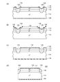
図16及び図17は、そのような従来の半導体装置の製造方法を説明するために示す図である。図16(a)〜図16(d)及び図17(a)〜図17(d)は各工程図である。
従来の半導体装置の製造方法は、図16及び図17に示すように、「半導体基体形成工程」、「溝形成工程」、「重金属拡散工程」、「ガラス層形成工程」、「ガラス保護膜形成工程」、「酸化膜除去工程」、「電極形成工程」及び「半導体基体切断工程」をこの順序で含む。以下、従来の半導体装置の製造方法を工程順に説明する。なお、この明細書において、溝を形成する側の主面のことを第1主面といい、その反対側の主面を第2主面ということとする。16 and 17 are views for explaining such a conventional method of manufacturing a semiconductor device. 16A to 16D and FIGS. 17A to 17D are process diagrams.
As shown in FIGS. 16 and 17, the conventional semiconductor device manufacturing method includes a “semiconductor substrate forming step”, a “groove forming step”, a “heavy metal diffusion step”, a “glass layer forming step”, and a “glass protective film forming”. Process, "oxide film removal process,""electrode formation process" and "semiconductor substrate cutting process" are included in this order. Hereinafter, a conventional method for manufacturing a semiconductor device will be described in the order of steps. In this specification, the main surface on the side where grooves are formed is referred to as a first main surface, and the main surface on the opposite side is referred to as a second main surface.
(a)半導体基体形成工程
まず、n−型半導体層(n−型シリコン基板)910の第2主面側の表面からのn型不純物の拡散によりn+型半導体層914を形成し、第1主面側の表面からのp型不純物の拡散によりp+型半導体層912を形成して主面に平行なpn接合が形成された半導体基体を形成する。なお、n+型半導体層(n+型シリコン基板)にn−型半導体層(n−型エピタキシャル層)を形成した後、当該n−型半導体層(n−型エピタキシャル層)の表面からのp型不純物の拡散によりp+型半導体層を形成して主面に平行なpn接合が形成された半導体基体を形成してもよい。その後、熱酸化によりp+型半導体層912及びn+型半導体層914の表面に酸化膜916,918を形成する(図16(a)参照。)。(A) Semiconductor Substrate Formation Step First, an n + -
(b)溝形成工程
次に、フォトエッチング法によって、酸化膜916の所定部位に所定の開口部を形成する。酸化膜のエッチング後、引き続いて半導体基体のエッチングを行い、半導体基体の第1主面側の表面からpn接合を超える深さの溝(この場合、n−型半導体層910とn+型半導体層914との境界面をも超える深さの溝)920を形成する(図16(b)参照。)。このとき、溝の内面にpn接合露出部Aが形成される。(B) Groove Formation Step Next, a predetermined opening is formed at a predetermined portion of the
(c)重金属拡散工程
次に、半導体基体の第2主面側の表面から酸化膜918を除去した後、当該半導体基体の第2主面側の表面に、重金属(例えばPt)をスパッタ法により形成したり、重金属(例えばPt)を溶液にしてスピンオンする等の方法により塗布したりして、半導体基体の第2主面側の表面に、重金属拡散源となる層922を形成する。その後、所定の温度で重金属を熱拡散させて半導体基体の内部にキャリアの再結合中心を形成する(図16(c)参照。)。なお、重金属拡散工程は、上記した溝形成工程の前に実施してもよい。(C) Heavy metal diffusion step Next, after removing the
(d)ガラス層形成工程
次に、重金属拡散源となる層922を除去した後、溝920の表面に、電気泳動法により溝920の内面及びその近傍の半導体基体表面に半導体接合保護用ガラス組成物からなる層を形成するとともに、当該半導体接合保護用ガラス組成物からなる層を焼成することにより、パッシベーション用のガラス層926を形成する(図16(d)参照。)。このとき、半導体基体の第2主面側に酸化膜924が形成される。(D) Glass layer forming step Next, after removing the
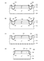
(e)ガラス保護膜形成工程
次に、ガラス層926の表面を覆うようにガラス保護膜(例えばピッチ系ワックス類からなるガラス保護膜)928を形成する(図17(a)参照。)。(E) Glass Protective Film Formation Step Next, a glass protective film (for example, a glass protective film made of pitch wax) 928 is formed so as to cover the surface of the glass layer 926 (see FIG. 17A).
(f)酸化膜除去工程
次に、ガラス保護膜928をマスクとして酸化膜916のエッチングを行い、電極形成領域930における酸化膜916及び半導体基体の第2主面側の表面に形成されていた酸化膜924を除去する(図17(b)参照。)。
(F) Oxide Film Removal Step Next, the
(g)電極形成工程
次に、半導体基体にNiめっきを行い、半導体基体の第1主面側の表面における電極形成領域930にアノード電極932を形成するとともに、半導体基体の第2主面側の表面にカソード電極934を形成する(図17(c)参照。)。なお、Niめっきに代えて蒸着、スパッタ等の気相法によりアノード電極及びカソード電極を形成してもよい。(G) Electrode formation step Next, Ni plating is performed on the semiconductor substrate to form an
(h)半導体基体切断工程
次に、ダイシング等により、ガラス層926の中央部において半導体基体を切断して半導体基体をチップ化して、メサ型半導体装置(pnダイオード)900を作製する(図17(d)参照。)。(H) Semiconductor Substrate Cutting Step Next, the mesa semiconductor device (pn diode) 900 is fabricated by cutting the semiconductor substrate at the center of the
以上説明したように、従来の半導体装置の製造方法は、主面に平行なpn接合が形成された半導体基体の第1主面側の表面からpn接合を超える溝920を形成する工程(図16(a)及び図16(b)参照。)と、溝920の内部にpn接合露出部を覆うようにパッシベーション用のガラス層926を形成する工程(図16(d)参照。)とを含む。このため、従来の半導体装置の製造方法によれば、溝920の内部にパッシベーション用のガラス層926を形成した後半導体基体を切断することにより、高信頼性のメサ型半導体装置を製造することができる。
As described above, in the conventional method for manufacturing a semiconductor device, the step of forming a
また、従来の半導体装置の製造方法は、半導体基体の第2主面側の表面から重金属を熱拡散させて半導体基体の内部にキャリアの再結合中心を形成する工程(図16(c)参照。)を含む。このため、従来の半導体装置の製造方法によれば、逆回復時間trrが短くスイッチング特性に優れた半導体装置を製造することができる。 Further, in the conventional method for manufacturing a semiconductor device, a heavy metal is thermally diffused from the surface on the second main surface side of the semiconductor substrate to form a carrier recombination center in the semiconductor substrate (see FIG. 16C). )including. For this reason, according to the conventional method for manufacturing a semiconductor device, a semiconductor device having a short reverse recovery time trr and excellent switching characteristics can be manufactured.
ところで、パッシベーション用のガラス層に用いるガラス材料としては、(a)適正な温度で焼成できること、(b)工程で使用する薬品に耐えること、(c)優れた絶縁性を有すること、及び(d)半導体装置の特性を悪くしないことという条件を満たす必要があることから、従来より「珪酸鉛を主成分としたガラス材料」が広く用いられている。 By the way, as a glass material used for the glass layer for passivation, (a) it can be baked at an appropriate temperature, (b) can withstand chemicals used in the process, (c) has excellent insulating properties, and (d ) Since it is necessary to satisfy the condition of not deteriorating the characteristics of the semiconductor device, “a glass material mainly composed of lead silicate” has been widely used.
しかしながら、「珪酸鉛を主成分としたガラス材料」には環境負荷の大きい鉛が含まれており、近未来にはそのような「珪酸鉛を主成分としたガラス材料」の使用が禁止されていくことになると考えられる。 However, “glass material based on lead silicate” contains lead with a large environmental impact, and in the near future, the use of such “glass material based on lead silicate” is prohibited. It is thought that it will go.
なお、このような事情は、メサ型の半導体装置を製造する半導体装置の製造方法の場合だけに存在するのではなく、プレーナ型の半導体装置を製造する半導体装置の製造方法をはじめpn接合露出部を覆うようにパッシベーション用のガラス層を形成して高信頼性の半導体装置を製造する半導体装置の製造方法全般に存在する。 Such a situation does not exist only in the case of a semiconductor device manufacturing method for manufacturing a mesa type semiconductor device, but also a pn junction exposed portion including a semiconductor device manufacturing method for manufacturing a planar type semiconductor device. In general, there are semiconductor device manufacturing methods for manufacturing a highly reliable semiconductor device by forming a passivation glass layer so as to cover the substrate.
そこで、本発明は、上記した事情に鑑みてなされたもので、鉛を含まないガラス材料を用いて、従来の「珪酸鉛を主成分としたガラス材料」を用いた場合と同様に高信頼性の半導体装置を製造することを可能とする、半導体接合保護用ガラス組成物、半導体装置の製造方法及び半導体装置を提供することを目的とする。 Therefore, the present invention has been made in view of the above circumstances, and uses a glass material that does not contain lead, and has high reliability as in the case of using a conventional “glass material mainly composed of lead silicate”. An object of the present invention is to provide a glass composition for protecting a semiconductor junction, a method for manufacturing a semiconductor device, and a semiconductor device, which make it possible to manufacture the semiconductor device.
[1]本発明の半導体接合保護用ガラス組成物は、pn接合が露出するpn接合露出部を有する半導体素子におけるpn接合を保護するガラス層を形成するための半導体接合保護用ガラス組成物であって、少なくともZnOと、SiO2と、B2O3と、Al2O3と、BaO、CaO及びMgOのうち少なくとも2つのアルカリ土類金属の酸化物とを以下の含有量で含有し、かつ、Pbと、Asと、Sbと、Liと、Naと、Kとを実質的に含有しないガラス原料を溶融させて得られる融液から作製されたガラス微粒子からなり、かつ、フィラーを含まないことを特徴とする。
−−−−−−−−−−−−−−−−−−−−−−−−−−−−−−−
ZnO:30mol%〜60mol%
SiO2:5mol%〜45mol%
B2O3:5mol%〜30mol%
Al2O3:5mol%〜13mol%
アルカリ土類金属の酸化物:1mol%〜10mol%
−−−−−−−−−−−−−−−−−−−−−−−−−−−−−−−[1] The glass composition for protecting a semiconductor junction according to the present invention is a glass composition for protecting a semiconductor junction for forming a glass layer for protecting a pn junction in a semiconductor element having a pn junction exposed portion where the pn junction is exposed. And at least ZnO, SiO 2 , B 2 O 3 , Al 2 O 3 and at least two alkaline earth metal oxides of BaO, CaO and MgO in the following content, and Made of glass fine particles made from a melt obtained by melting glass raw materials substantially free of Pb, As, Sb, Li, Na, and K, and does not contain a filler It is characterized by.
------------------------------
ZnO: 30 mol% to 60 mol%
SiO 2: 5mol% ~45mol%
B 2 O 3: 5mol% ~30mol %
Al 2 O 3: 5mol% ~13mol %
Alkaline earth metal oxides: 1 mol% to 10 mol%
------------------------------
[2]本発明の半導体接合保護用ガラス組成物においては、前記ガラス原料がBiを実質的に含有しないことが好ましい。 [2] In the glass composition for protecting a semiconductor junction according to the present invention, it is preferable that the glass raw material does not substantially contain Bi.
[3]本発明の半導体接合保護用ガラス組成物においては、前記ガラス原料がPを実質的に含有しないことが好ましい。 [3] In the glass composition for protecting a semiconductor junction according to the present invention, it is preferable that the glass raw material does not substantially contain P.
[4]本発明の半導体接合保護用ガラス組成物においては、前記ガラス原料がニッケル酸化物をさらに含有することを好ましい。 [4] In the glass composition for protecting a semiconductor junction according to the present invention, it is preferable that the glass raw material further contains a nickel oxide.
[5]本発明の半導体接合保護用ガラス組成物においては、前記ガラス原料がZrO2をさらに含有することが好ましい。[5] In the glass composition for protecting a semiconductor junction according to the present invention, it is preferable that the glass raw material further contains ZrO 2 .
[6]本発明の半導体接合保護用ガラス組成物においては、前記ガラス層が、絶縁層を介して前記pn接合露出部を覆うように形成されてなるガラス層であることが好ましい。 [6] In the glass composition for protecting a semiconductor junction according to the present invention, the glass layer is preferably a glass layer formed so as to cover the pn junction exposed portion via an insulating layer.
[7]本発明の半導体接合保護用ガラス組成物においては、ガラス転移温度Tgが540℃〜680℃の範囲内にあることが好ましい。 [7] In the glass composition for protecting a semiconductor junction of the present invention, the glass transition temperature Tg is preferably in the range of 540 ° C to 680 ° C.
[8]本発明の半導体接合保護用ガラス組成物においては。50℃〜500℃の温度範囲における平均線膨張率が4.5×10⁻⁶〜5.8×10⁻⁶の範囲内にあることが好ましい。[8] In the glass composition for protecting a semiconductor junction of the present invention. It is preferable that the average linear expansion coefficient in the temperature range of 50 ° C. to 500 ° C. is in the range of 4.5 × 10 −6 to 5.8 × 10 −6 .
[9]本発明の半導体接合保護用ガラス組成物においては、ZnOの含有量が40mol%〜56mol%の範囲内にあり、SiO2の含有量が8mol%〜20mol%の範囲内にあり、B2O3の含有量が20mol%〜30mol%の範囲内にあり、Al2O3の含有量が6mol%〜10mol%の範囲内にあり、アルカリ土類金属の酸化物の含有量が2mol%〜5mol%の範囲内にあることが好ましい。[9] In the glass composition for protecting a semiconductor junction of the present invention are within the content of ZnO is 40mol% ~56mol%, the content of SiO 2 is within the range of 8
[10]本発明の半導体接合保護用ガラス組成物においては、前記半導体素子がSi製の半導体素子であることが好ましい。 [10] In the glass composition for protecting a semiconductor junction according to the present invention, the semiconductor element is preferably a Si semiconductor element.
[11]本発明の半導体接合保護用ガラス組成物においては、前記半導体素子がファーストリカバリダイオードであることが好ましい。 [11] In the glass composition for protecting a semiconductor junction according to the present invention, the semiconductor element is preferably a first recovery diode.
[12]本発明の半導体接合保護用ガラス組成物においては、前記半導体素子がSiC製の半導体素子であることが好ましい。 [12] In the glass composition for protecting a semiconductor junction according to the present invention, the semiconductor element is preferably a SiC semiconductor element.
[13]本発明の半導体接合保護用ガラス組成物においては、前記半導体素子がGaN製の半導体素子であることが好ましい。 [13] In the glass composition for protecting a semiconductor junction according to the present invention, the semiconductor element is preferably a GaN semiconductor element.
[14]本発明の半導体装置の製造方法は、pn接合が露出するpn接合露出部を有する半導体素子を準備する第1工程と、前記pn接合露出部を覆うようにガラス層を形成する第2工程とをこの順序で含む半導体装置の製造方法であって、前記第2工程においては、少なくともZnOと、SiO2と、B2O3と、Al2O3と、BaO、CaO及びMgOのうち少なくとも2つのアルカリ土類金属の酸化物とを以下の含有量で含有し、かつ、Pbと、Asと、Sbと、Liと、Naと、Kとを実質的に含有しないガラス原料を溶融させて得られる融液から作製されたガラス微粒子からなり、かつ、フィラーを含まない半導体接合保護用ガラス組成物を用いて前記ガラス層を形成することを特徴とする。
−−−−−−−−−−−−−−−−−−−−−−−−−−−−−−−
ZnO:30mol%〜60mol%
SiO2:5mol%〜45mol%
B2O3:5mol%〜30mol%
Al2O3:5mol%〜13mol%
アルカリ土類金属の酸化物:1mol%〜10mol%
−−−−−−−−−−−−−−−−−−−−−−−−−−−−−−−[14] A method for manufacturing a semiconductor device according to the present invention includes a first step of preparing a semiconductor element having a pn junction exposed portion where a pn junction is exposed, and a second step of forming a glass layer so as to cover the pn junction exposed portion. and a step method for manufacturing a semiconductor device comprising in this order, wherein in the second step, at least ZnO, and SiO 2, and
------------------------------
ZnO: 30 mol% to 60 mol%
SiO 2: 5mol% ~45mol%
B 2 O 3: 5mol% ~30mol %
Al 2 O 3: 5mol% ~13mol %
Alkaline earth metal oxides: 1 mol% to 10 mol%
------------------------------
[15]本発明の半導体装置の製造方法においては、前記第2工程は、前記pn接合露出部上に絶縁膜を形成する工程と、前記絶縁膜を介して前記pn接合露出部を覆うように前記ガラス層を形成する工程とを含むことが好ましい。 [15] In the method of manufacturing a semiconductor device according to the present invention, the second step includes a step of forming an insulating film on the pn junction exposed portion, and the pn junction exposed portion is covered via the insulating film. And forming the glass layer.
[16]本発明の半導体装置は、pn接合が露出するpn接合露出部を有する半導体素子と、前記pn接合露出部を覆うように形成されたガラス層とを備える半導体装置であって、前記ガラス層は、少なくともZnOと、SiO2と、B2O3と、Al2O3と、BaO、CaO及びMgOのうち少なくとも2つのアルカリ土類金属の酸化物とを以下の含有量で含有し、かつ、Pbと、Asと、Sbと、Liと、Naと、Kとを実質的に含有しないガラス原料を溶融させて得られる融液から作製されたガラス微粒子からなり、かつ、フィラーを含まない半導体接合保護用ガラス組成物を用いて形成されたものであることを特徴とする。
−−−−−−−−−−−−−−−−−−−−−−−−−−−−−−−
ZnO:30mol%〜60mol%
SiO2:5mol%〜45mol%
B2O3:5mol%〜30mol%
Al2O3:5mol%〜13mol%
アルカリ土類金属の酸化物:1mol%〜10mol%
−−−−−−−−−−−−−−−−−−−−−−−−−−−−−−−[16] A semiconductor device of the present invention is a semiconductor device comprising a semiconductor element having a pn junction exposed portion where a pn junction is exposed, and a glass layer formed so as to cover the pn junction exposed portion, wherein the glass The layer contains at least ZnO, SiO 2 , B 2 O 3 , Al 2 O 3 , and an oxide of at least two alkaline earth metals of BaO, CaO, and MgO in the following contents: And it consists of the glass fine particle produced from the melt obtained by melting the glass raw material which does not contain Pb, As, Sb, Li, Na, and K substantially, and does not contain a filler. It is formed using the glass composition for semiconductor junction protection, It is characterized by the above-mentioned.
------------------------------
ZnO: 30 mol% to 60 mol%
SiO 2: 5mol% ~45mol%
B 2 O 3: 5mol% ~30mol %
Al 2 O 3: 5mol% ~13mol %
Alkaline earth metal oxides: 1 mol% to 10 mol%
------------------------------
[17]本発明の半導体装置においては、前記ガラス層は、絶縁層を介して前記pn接合露出部を覆うように形成されてなることが好ましい。 [17] In the semiconductor device of the present invention, it is preferable that the glass layer is formed so as to cover the pn junction exposed portion via an insulating layer.
本発明の半導体接合保護用ガラス組成物、半導体装置の製造方法及び半導体装置によれば、後述する実施例からも分かるように、鉛を含まないガラス材料を用いて、従来の「珪酸鉛を主成分としたガラス材料」を用いた場合と同様に高信頼性の半導体装置を製造することが可能となる。 According to the glass composition for protecting a semiconductor junction, the method for manufacturing a semiconductor device, and the semiconductor device of the present invention, as can be seen from the examples described later, a glass material that does not contain lead is used. It becomes possible to manufacture a highly reliable semiconductor device as in the case of using “glass material as a component”.
また、本発明の半導体接合保護用ガラス組成物、半導体装置の製造方法及び半導体装置によれば、少なくともZnOと、SiO2と、B2O3と、Al2O3と、BaO、CaO及びMgOのうち少なくとも2つのアルカリ土類金属の酸化物とを上記の含有量で含有し、かつ、Pbと、Asと、Sbと、Liと、Naと、Kとを実質的に含有しないガラス原料を溶融させて得られる融液から作製されたガラス微粒子からなる半導体接合保護用ガラス組成物からなる層を焼成することによりガラス層を形成するようにしたことから、半導体接合保護用ガラス組成物のガラス転移温度Tgが540℃〜680℃と低く、後述する実施例からも明らかなように、従来の「珪酸鉛を主成分としたガラス材料」よりも半導体接合保護用ガラス組成物からなる層を焼成する際の焼成温度を低くすることが可能となる(例えば600℃〜760℃)。Further, the glass composition for protecting a semiconductor junction of the present invention, according to the method of manufacturing a semiconductor device, and at least ZnO, and SiO 2, and
その結果、本発明の半導体接合保護用ガラス組成物、半導体装置の製造方法及び半導体装置によれば、半導体素子の製造過程(半導体接合保護用ガラス組成物を焼成する工程)中にキャリアの再結合中心がアニールされて減少するためにスイッチング特性が悪化し易い半導体装置(例えば逆回復時間trrが長くなり易いファーストリカバリーダイオード)を製造する場合であっても、半導体素子の製造過程(半導体接合保護用ガラス組成物を焼成する工程)中にスイッチング特性が悪化し難くなり、スイッチング特性の優れた半導体装置を製造することが可能となる。 As a result, according to the glass composition for protecting a semiconductor junction, the method for manufacturing a semiconductor device, and the semiconductor device of the present invention, recombination of carriers during the process of manufacturing a semiconductor element (step of firing the glass composition for protecting a semiconductor junction). Even when manufacturing a semiconductor device (for example, a fast recovery diode in which the reverse recovery time trr tends to be long) whose switching characteristics are likely to deteriorate because the center is annealed and reduced, the semiconductor element manufacturing process (for semiconductor junction protection) During the step of firing the glass composition, the switching characteristics are unlikely to deteriorate, and a semiconductor device having excellent switching characteristics can be produced.
また、上記の結果、本発明の半導体接合保護用ガラス組成物、半導体装置の製造方法及び半導体装置によれば、半導体素子の製造過程(半導体接合保護用ガラス組成物を焼成する工程)中にガラス層が結晶化し難くなり、逆方向リーク電流IRの低い半導体装置を製造することが可能となる。この場合、半導体基体とガラス層との間に下地酸化膜を設けなくとも逆方向リーク電流IRの低い半導体装置を安定して製造することが可能となる(後述する実施形態4及び実施例2〜6参照。)。
Moreover, according to said result, according to the glass composition for semiconductor junction protection of this invention, the manufacturing method of a semiconductor device, and a semiconductor device, it is glass during the manufacturing process (process of baking the glass composition for semiconductor junction protection) of a semiconductor element. The layer becomes difficult to crystallize, and a semiconductor device having a low reverse leakage current IR can be manufactured. In this case, it is possible to stably manufacture a semiconductor device having a low reverse leakage current IR without providing a base oxide film between the semiconductor substrate and the glass layer (
ところで、半導体接合保護用ガラス組成物として、フィラーを含む半導体接合保護用ガラス組成物を用いた場合には、pn接合を覆うように半導体接合保護用ガラス組成物からなる層を形成する際に当該半導体接合保護用ガラス組成物からなる層を均一に形成することが困難となる場合がある。すなわち、電気泳動法により半導体接合保護用ガラス組成物からなる層を形成する場合には、電気泳動の不均一により半導体接合保護用ガラス組成物からなる層を均一に形成することが困難となり、スピンコート法、スクリーン印刷法、ドクターブレード法により半導体接合保護用ガラス組成物からなる層を形成する場合には、粒径や比重などの違いにより半導体接合保護用ガラス組成物からなる層を均一に形成することが困難となる場合がある。 By the way, when the glass composition for semiconductor junction protection containing a filler is used as the glass composition for semiconductor junction protection, when the layer made of the glass composition for semiconductor junction protection is formed so as to cover the pn junction, It may be difficult to uniformly form a layer made of a glass composition for protecting a semiconductor junction. That is, when a layer made of a glass composition for protecting a semiconductor junction is formed by electrophoresis, it becomes difficult to uniformly form a layer made of the glass composition for protecting a semiconductor junction due to non-uniform electrophoresis. coating method, a screen printing method, in the case of forming a layer made of glass composition for protecting a semiconductor junction by a doctor blade method, a layer made of a semi-conductor junction protective glass composition by differences in particle size and specific gravity uniformly It may be difficult to form.
これに対して、本発明の半導体接合保護用ガラス組成物、半導体装置の製造方法及び半導体装置によれば、半導体接合保護用ガラス組成物として、フィラーを含まない半導体接合保護用ガラス組成物からなる層を用いたことから、pn接合を覆うように半導体接合保護用ガラス組成物からなる層を形成する際に当該半導体接合保護用ガラス組成物からなる層を均一に形成することが可能となる。 On the other hand, according to the glass composition for semiconductor junction protection, the method for manufacturing a semiconductor device, and the semiconductor device of the present invention, the glass composition for semiconductor junction protection comprises a glass composition for semiconductor junction protection that does not contain a filler. Since the layer is used, when the layer made of the glass composition for protecting a semiconductor junction is formed so as to cover the pn junction, the layer made of the glass composition for protecting a semiconductor junction can be formed uniformly.
なお、本発明の半導体接合保護用ガラス組成物、半導体装置の製造方法及び半導体装置において、少なくともある特定成分(ZnO、SiO2等)を含有するとは、当該ある特定成分のみを含有する場合のほか、当該ある特定成分に加えて、ガラス組成物に通常含有可能な成分をさらに含有する場合も含む。In addition, in the glass composition for semiconductor junction protection of the present invention, the method for manufacturing a semiconductor device, and the semiconductor device, it contains at least a specific component (ZnO, SiO 2, etc.) in addition to the case where only the specific component is included. In addition to the specific component, the case where the glass composition further contains a component that can usually be contained is also included.
また、本発明の半導体接合保護用ガラス組成物、半導体装置の製造方法及び半導体装置において、ある特定元素(Pb、As等)を実質的に含有しないとは、当該ある特定元素を成分として含有しないという意味であり、ガラスを構成する各成分のガラス原料中に不純物として上記ある特定元素が混入したガラス組成物を排除するものではない。 Further, in the glass composition for protecting a semiconductor junction, the method for manufacturing a semiconductor device, and the semiconductor device of the present invention, the fact that a certain element (Pb, As, etc.) is not substantially contained does not contain the certain element as a component. This does not exclude a glass composition in which the above-mentioned specific element is mixed as an impurity in the glass raw material of each component constituting the glass.
また、本発明の半導体接合保護用ガラス組成物、半導体装置の製造方法及び半導体装置において、ある特定元素(Pb、As等)を含有しないとは、当該ある特定元素の酸化物、当該ある特定元素の窒化物等を含有しないことをいう。 Further, in the glass composition for protecting a semiconductor junction of the present invention, the method for manufacturing a semiconductor device, and the semiconductor device, it does not contain a specific element (Pb, As, etc.) means that the oxide of the specific element, the specific element This means that it contains no nitride or the like.
ここで、Pbを実質的に含有しないこととしたのは、本発明の目的が「鉛を含まないガラス材料を用いて、従来の「珪酸鉛を主成分としたガラス材料」を用いた場合と同様に高信頼性の半導体装置を製造することを可能とする」ことにあるからである。 Here, Pb is not substantially contained because the purpose of the present invention is to use a conventional “glass material containing lead silicate as a main component using a glass material not containing lead”. Similarly, it is possible to manufacture a highly reliable semiconductor device ”.
また、Asと、Sbとを実質的に含有しないこととしたのは、これらの成分は毒性を有するため、これらの成分の使用を制限する動きが広がりつつあるからである。 The reason why As and Sb are not substantially contained is because these components are toxic, and movements to limit the use of these components are spreading.
また、Liと、Naと、Kとを実質的に含有しないこととしたのは、これらの成分を含有する場合には平均線膨張率や焼成温度の点では有利なのではあるが、絶縁性が低下する場合があるからである。 In addition, the fact that Li, Na, and K are not substantially contained is advantageous in terms of average linear expansion coefficient and firing temperature when these components are contained, This is because it may decrease.
以下、本発明の半導体接合保護用ガラス組成物、半導体装置の製造方法及び半導体装置について、図に示す実施の形態に基づいて説明する。 Hereinafter, a glass composition for protecting a semiconductor junction, a method for manufacturing a semiconductor device, and a semiconductor device of the present invention will be described based on the embodiments shown in the drawings.
[実施形態1]
実施形態1は、半導体接合保護用ガラス組成物に係る実施形態である。特に、後述する実施例3〜6に係る半導体接合保護用ガラス組成物を含む実施形態である。[Embodiment 1]
実施形態1に係る半導体接合保護用ガラス組成物は、pn接合が露出するpn接合露出部を有する半導体素子におけるpn接合を保護するガラス層を形成するための半導体接合保護用ガラス組成物であって、少なくともZnOと、SiO2と、B2O3と、Al2O3と、BaO、CaO及びMgOのうち少なくとも2つのアルカリ土類金属の酸化物と、ZrO2と、ニッケル酸化物とを以下の含有量で含有し、かつ、Pbと、Asと、Sbと、Liと、Naと、Kとを実質的に含有しないガラス原料を溶融させて得られる融液から作製されたガラス微粒子からなり、かつ、フィラーを含まないものである。
−−−−−−−−−−−−−−−−−−−−−−−−−−−−−−−
ZnO:30mol%〜60mol%
SiO2:5mol%〜45mol%
B2O3:5mol%〜30mol%
Al2O3:5mol%〜13mol%
アルカリ土類金属の酸化物:1mol%〜10mol%
ZrO2:0.1mol%〜3.0mol%
ニッケル酸化物:0.01mol%〜2.0mol%
−−−−−−−−−−−−−−−−−−−−−−−−−−−−−−−The glass composition for semiconductor junction protection which concerns on
------------------------------
ZnO: 30 mol% to 60 mol%
SiO 2: 5mol% ~45mol%
B 2 O 3: 5mol% ~30mol %
Al 2 O 3: 5mol% ~13mol %
Alkaline earth metal oxides: 1 mol% to 10 mol%
ZrO2: 0.1 mol% to 3.0 mol%
Nickel oxide: 0.01 mol% to 2.0 mol%
------------------------------
実施形態1に係る半導体接合保護用ガラス組成物においては、ガラス原料は、アルカリ土類金属の酸化物として、BaO、CaO及びMgOのうちすべてを含有するものであってもよいし、BaO、CaO及びMgOのうち2つ(例えばBaO及びCaO)を含有するものであってもよい。
In the glass composition for protecting a semiconductor junction according to
実施形態1に係る半導体接合保護用ガラス組成物においては、ガラス原料がBi及びPを実質的に含有しないものであることが好ましい。
In the glass composition for protecting a semiconductor junction according to
実施形態1に係る半導体接合保護用ガラス組成物は、ガラス転移温度Tgが540℃〜680℃の範囲内にある。また、実施形態1に係る半導体接合保護用ガラス組成物は、50℃〜500℃の温度範囲における平均線膨張率が4.5×10⁻⁶〜5.8×10⁻⁶の範囲内にある。The glass composition for semiconductor junction protection according to
実施形態1に係る半導体接合保護用ガラス組成物によれば、後述する実施例からも明らかなように、鉛を含まないガラス材料を用いて、従来の「珪酸鉛を主成分としたガラス材料」を用いた場合と同様に高信頼性の半導体装置を製造することが可能となる。 According to the glass composition for protecting a semiconductor junction according to the first embodiment, as is clear from examples described later, a conventional “glass material mainly composed of lead silicate” using a glass material not containing lead. It becomes possible to manufacture a highly reliable semiconductor device in the same manner as in the case of using.
また、実施形態1に係る半導体接合保護用ガラス組成物によれば、少なくともZnOと、SiO2と、B2O3と、Al2O3と、BaO、CaO及びMgOのうち少なくとも2つのアルカリ土類金属の酸化物とを上記の含有量で含有し、かつ、Pbと、Asと、Sbと、Liと、Naと、Kとを実質的に含有しないガラス原料を溶融させて得られる融液から作製されたガラス微粒子からなる半導体接合保護用ガラス組成物であることから、ガラス転移温度Tgが540℃〜680℃と低く、後述する実施例からも明らかなように、従来の「珪酸鉛を主成分としたガラス材料」よりも半導体接合保護用ガラス組成物からなる層を焼成する際の焼成温度を低くすることが可能となる(例えば600℃〜760℃)。Further, according to the glass composition for protecting a semiconductor junction according to the first embodiment, at least ZnO, and SiO 2, and
その結果、実施形態1に係る半導体接合保護用ガラス組成物によれば、半導体素子の製造過程(半導体接合保護用ガラス組成物を焼成する工程)中にキャリアの再結合中心がアニールされて減少するためにスイッチング特性が悪化し易い半導体装置(例えば逆回復時間trrが長くなり易いファーストリカバリーダイオード)を製造する場合であっても、半導体素子の製造過程(半導体接合保護用ガラス組成物を焼成する工程)中にスイッチング特性が悪化し難くなり、スイッチング特性の優れた半導体装置を製造することが可能となる。 As a result, according to the glass composition for protecting a semiconductor junction according to the first embodiment, the recombination centers of carriers are reduced by annealing during the manufacturing process of the semiconductor element (the step of firing the glass composition for protecting a semiconductor junction). Therefore, even when a semiconductor device whose switching characteristics are likely to deteriorate (for example, a fast recovery diode whose reverse recovery time trr tends to be long) is manufactured, a semiconductor element manufacturing process (a step of baking a glass composition for protecting a semiconductor junction) ), The switching characteristics are hardly deteriorated, and a semiconductor device having excellent switching characteristics can be manufactured.
また、上記の結果、実施形態1に係る半導体接合保護用ガラス組成物によれば、半導体素子の製造過程(半導体接合保護用ガラス組成物を焼成する工程)中にガラス層が結晶化し難くなり、逆方向リーク電流IRの低い半導体装置を製造することが可能となる。従って、半導体基体とガラス層との間に下地酸化膜を設けなくとも逆方向リーク電流IRの低い半導体装置を安定して製造することが可能となる(後述する実施形態4及び実施例3〜6参照。)。
As a result, according to the glass composition for protecting a semiconductor junction according to the first embodiment, the glass layer is hardly crystallized during the manufacturing process of the semiconductor element (step of firing the glass composition for protecting the semiconductor junction). A semiconductor device with a low reverse leakage current IR can be manufactured. Therefore, it is possible to stably manufacture a semiconductor device having a low reverse leakage current IR without providing a base oxide film between the semiconductor substrate and the glass layer (
また、実施形態1に係る半導体接合保護用ガラス組成物によれば、半導体接合保護用ガラス組成物として、フィラーを含まない半導体接合保護用ガラス組成物からなる層を用いたことから、pn接合を覆うように半導体接合保護用ガラス組成物からなる層を形成する際に当該半導体接合保護用ガラス組成物からなる層を均一に形成することが可能となる。
Moreover, according to the glass composition for semiconductor junction protection which concerns on
なお、実施形態1に係る半導体接合保護用ガラス組成物のなかでも、後述する実施例3、4及び6の半導体接合保護用ガラス組成物を含む半導体接合保護用ガラス組成物、すなわち、ZnOの含有量が40mol%〜56mol%の範囲内にあり、SiO2の含有量が8mol%〜20mol%の範囲内にあり、B2O3の含有量が20mol%〜30mol%の範囲内にあり、Al2O3の含有量が6mol%〜10mol%の範囲内にあり、アルカリ土類金属の酸化物の含有量が2mol%〜5mol%の範囲内にある半導体接合保護用ガラス組成物によれば、ガラス転移温度Tgが540℃〜620℃とより一層低くなり、後述する実施例からも明らかなように、従来の「珪酸鉛を主成分としたガラス材料」よりも半導体接合保護用ガラス組成物からなる層を焼成する際の焼成温度をより一層低くすることが可能となる(例えば600℃〜730℃)。In addition, among the glass compositions for semiconductor junction protection which concern on
また、実施形態1に係る半導体接合保護用ガラス組成物によれば、50℃〜500℃の温度範囲における平均線膨張率を半導体材料(Si、SiC、GaN)の線膨張率(Si:3.7×10⁻⁶、SiC:4.4×10⁻⁶、GaN:5.6×10⁻⁶)に近い値(例えば4.8×10⁻⁶〜5.8×10⁻⁶)にすることができる。このため、工程中におけるウェーハの反りが小さくなることから、薄型ウェーハを使用して順方向特性に優れた半導体装置を製造することが可能となり、また、ガラス層の厚さを厚くして逆方向特性に優れた半導体装置を製造することが可能となる。Moreover, according to the glass composition for semiconductor junction protection which concerns on
ここで、ZnOの含有量を30mol%〜60mol%の範囲内としたのは、ZnOの含有量が30mol%未満である場合には、焼成温度が高くなる傾向にあるからであり、ZnOの含有量が60mol%を超える場合には、耐薬品性が低下したり、絶縁性が低下したりする場合があり、さらには、ガラス化の過程で結晶化し易くなる傾向にあるからである。 Here, the reason why the ZnO content is in the range of 30 mol% to 60 mol% is that when the ZnO content is less than 30 mol%, the firing temperature tends to increase. When the amount exceeds 60 mol%, chemical resistance may be lowered or insulation may be lowered, and further, crystallization tends to be easily caused during vitrification.
また、SiO2の含有量を5mol%〜45mol%の範囲内としたのは、SiO2の含有量が5mol%未満である場合には、耐薬品性が低下したり、絶縁性が低下したりする場合があるからであり、SiO2の含有量が45mol%を超える場合には、焼成温度が高くなる傾向にあるからである。In addition, the content of SiO 2 is set in the range of 5 mol% to 45 mol% because when the content of SiO 2 is less than 5 mol%, the chemical resistance is lowered or the insulation is lowered. This is because the firing temperature tends to increase when the SiO 2 content exceeds 45 mol%.
また、B2O3の含有量を5mol%〜30mol%の範囲内としたのは、B2O3の含有量が5mol%未満である場合には、焼成温度が高くなる傾向があるからであり、B2O3の含有量が30mol%を超える場合には、平均線膨張率が高くなる傾向にあるからである。The reason why the content of B 2 O 3 is in the range of 5 mol% to 30 mol% is that the firing temperature tends to increase when the content of B 2 O 3 is less than 5 mol%. This is because when the content of B 2 O 3 exceeds 30 mol%, the average linear expansion coefficient tends to increase.
また、Al2O3の含有量を5mol%〜13mol%の範囲内としたのは、Al2O3の含有量が5mol%未満である場合には、ガラス化の過程で結晶化し易くなる傾向にあるからであり、Al2O3の含有量が13mol%を超える場合には、絶縁性が低下する傾向にあるからである。In addition, the content of Al 2 O 3 is set within the range of 5 mol% to 13 mol% because when the content of Al 2 O 3 is less than 5 mol%, crystallization tends to occur during vitrification. This is because when the content of Al 2 O 3 exceeds 13 mol%, the insulating property tends to decrease.
また、アルカリ土類金属の酸化物の含有量を1mol%〜10mol%の範囲内としたのは、アルカリ土類金属の酸化物の含有量が1mol%未満である場合には、焼成温度が高くなる傾向にあるからであり、アルカリ土類金属の酸化物の含有量が10mol%を超える場合には、耐薬品性が低下したり、絶縁性が低下したりする場合があるからである。 In addition, the content of the alkaline earth metal oxide is in the range of 1 mol% to 10 mol% because the firing temperature is high when the content of the alkaline earth metal oxide is less than 1 mol%. This is because when the content of the alkaline earth metal oxide exceeds 10 mol%, the chemical resistance may be lowered or the insulation may be lowered.
なお、ここで、アルカリ土類金属酸化物として、少なくとも2つのアルカリ土類金属酸化物を含有させたのは、混合アルカリ効果(異なる原子半径を有する原子を複数含有することによりガラス化し易くなる効果)により焼成温度を低くできるからである。 Note that, here, at least two alkaline earth metal oxides were included as alkaline earth metal oxides because of the mixed alkali effect (the effect of facilitating vitrification by containing a plurality of atoms having different atomic radii). This is because the firing temperature can be lowered.
なお、ZrO2の含有量を0.1mol%〜3.0mol%の範囲内としたのは、ZrO2の含有量が0.1mol%未満である場合には、耐薬品性が低下したり、絶縁性が低下したりする場合があるからであり、ZrO2の含有量が3.0mol%を超える場合には、ガラスの溶融温度が高くなるからである。In addition, the content of ZrO 2 was set within the range of 0.1 mol% to 3.0 mol%, when the content of ZrO 2 is less than 0.1 mol%, the chemical resistance is reduced, This is because the insulating property may decrease, and when the ZrO 2 content exceeds 3.0 mol%, the melting temperature of the glass increases.
また、ニッケル酸化物の含有量を0.01mol%〜2.0mol%の範囲内としたのは、ニッケル酸化物の含有量が0.01mol%未満である場合には、「半導体接合保護用ガラス組成物からなる層」を焼成する過程で半導体基板との境界面から発生することのある泡の発生を抑制することが困難となる場合があるからであり、ニッケル酸化物の含有量が2.0mol%を超える場合には、ガラス化の過程で結晶化し易くなる傾向にあるからである。 Further, the content of nickel oxide is set within the range of 0.01 mol% to 2.0 mol% when the content of nickel oxide is less than 0.01 mol%, “glass for protecting semiconductor junctions”. This is because it may be difficult to suppress the generation of bubbles that may be generated from the interface with the semiconductor substrate in the process of firing the “layer composed of the composition”. This is because when it exceeds 0 mol%, crystallization tends to occur easily in the process of vitrification.
実施形態1に係る半導体接合保護用ガラス組成物は、以下のようにして製造することができる。すなわち、上記した組成比(モル比)になるようにガラス原料(ZnO、SiO2、H3BO3、Al2O3、BaCO3、CaCO3、MgO、ZrO2及びNiOを調合し、混合機でよく攪拌した後、その混合したガラス原料を白金ルツボに入れ、電気炉中で所定温度(例えば1250℃〜1350℃)・所定時間溶融させる。その後、融液を水冷ロールに流し出して薄片状のガラスフレークを得る。その後、このガラスフレークをボールミル等で所定の平均粒径となるまで粉砕して、粉末状のガラス組成物を得る。The glass composition for protecting a semiconductor junction according to
実施形態1に係る半導体接合保護用ガラス組成物は、Si製の半導体素子、SiC製の半導体素子又はGaN製の半導体素子のいずれの半導体素子にも好適に用いることができる。
The glass composition for protecting a semiconductor junction according to
実施形態1に係る半導体接合保護用ガラス組成物は、特に、半導体素子の製造過程(半導体接合保護用ガラス組成物を焼成する工程)中にキャリアの再結合中心がアニールされて減少するためにスイッチング特性が悪化し易い半導体装置(例えば逆回復時間trrが長くなり易いファーストリカバリーダイオード)に好適に用いることができる。
The glass composition for protecting a semiconductor junction according to
また、実施形態1に係る半導体接合保護用ガラス組成物は、50℃〜500℃の温度範囲における平均線膨張率が4.5×10⁻⁶〜5.8×10⁻⁶の範囲内にあることから、平均線膨張率の比較的高いSiC製の半導体素子(SiCの線膨張率:4.4×10⁻⁶)又はGaN製の半導体素子(GaNの線膨張率:5.6×10⁻⁶)にも好適に用いることができる。Further, the glass composition for protecting a semiconductor junction according to the
[実施形態2]
実施形態2は、半導体接合保護用ガラス組成物に係る実施形態である。特に、後述する実施例1に係る半導体接合保護用ガラス組成物を含む実施形態である。[Embodiment 2]
実施形態2に係る半導体接合保護用ガラス組成物は、基本的には実施形態1に係る半導体接合保護用ガラス組成物と同様の成分を含有するが、ニッケル酸化物を含有しない点で実施形態1に係る半導体接合保護用ガラス組成物とは異なる。すなわち、実施形態2に係る半導体接合保護用ガラス組成物は、基本的には実施形態1に係る半導体接合保護用ガラス組成物と同様の成分を含有するが、少なくともZnOと、SiO2と、B2O3と、Al2O3と、BaO、CaO及びMgOのうち少なくとも2つのアルカリ土類金属の酸化物と、ZrO2とを含有し、かつ、Pbと、Asと、Sbと、Liと、Naと、Kとを実質的に含有しないガラス原料を溶融させて得られる融液から作製されたガラス微粒子からなり、かつ、フィラーを含まないものである。The glass composition for protecting a semiconductor junction according to
実施形態2に係る半導体接合保護用ガラス組成物においては、ZnOの含有量、SiO2の含有量、B2O3の含有量、Al2O3の含有量、アルカリ土類金属の酸化物の含有量及びZrO2の含有量は、実施形態1に係る半導体接合保護用ガラス組成物の場合と同じである。
また、実施形態2に係る半導体接合保護用ガラス組成物は、実施形態1に係る半導体接合保護用ガラス組成物の場合とほぼ同様に、ガラス転移温度Tgが540℃〜680℃の範囲内にあり、50℃〜500℃の温度範囲における平均線膨張率が4.5×10⁻⁶〜5.8×10⁻⁶の範囲内にある。In the glass composition for protecting a semiconductor junction according to
Further, the glass composition for protecting a semiconductor junction according to
このように実施形態2に係る半導体接合保護用ガラス組成物は、ニッケル酸化物を含有しない点で、実施形態1に係る半導体接合保護用ガラス組成物と異なるが、鉛を含まないガラス材料を用いて、従来の「珪酸鉛を主成分としたガラス材料」を用いた場合と同様に高信頼性の半導体装置を製造することが可能となる。
Thus, although the glass composition for semiconductor junction protection which concerns on
また、実施形態2に係る半導体接合保護用ガラス組成物は、ZnOの含有量、SiO2の含有量、B2O3の含有量、Al2O3の含有量、アルカリ土類金属の酸化物の含有量及びZrO2の含有量が、実施形態1に係る半導体接合保護用ガラス組成物の場合と同じであることから、実施形態1に係る半導体接合保護用ガラス組成物の場合と同様に、ガラス転移温度Tgが540℃〜680℃と低く、後述する実施例からも明らかなように、従来の「珪酸鉛を主成分としたガラス材料」よりも半導体接合保護用ガラス組成物からなる層を焼成する際の焼成温度を低くすることが可能となる(例えば600℃〜760℃)。In addition, the glass composition for protecting a semiconductor junction according to the second embodiment includes a ZnO content, a SiO 2 content, a B 2 O 3 content, an Al 2 O 3 content, and an alkaline earth metal oxide. Since the content of ZrO 2 and the content of ZrO 2 are the same as in the case of the glass composition for protecting a semiconductor junction according to
その結果、実施形態2に係る半導体接合保護用ガラス組成物によれば、実施形態1に係る半導体接合保護用ガラス組成物の場合と同様に、半導体素子の製造過程(半導体接合保護用ガラス組成物を焼成する工程)中にキャリアの再結合中心がアニールされて減少するためにスイッチング特性が悪化し易い半導体装置(例えば逆回復時間trrが長くなり易いファーストリカバリーダイオード)を製造する場合であっても、半導体素子の製造過程(半導体接合保護用ガラス組成物を焼成する工程)中にスイッチング特性が悪化し難くなり、スイッチング特性の優れた半導体装置を製造することが可能となる。 As a result, according to the glass composition for protecting a semiconductor junction according to the second embodiment, as in the case of the glass composition for protecting a semiconductor junction according to the first embodiment, the manufacturing process of the semiconductor element (the glass composition for protecting the semiconductor junction). Even when a semiconductor device (for example, a fast recovery diode in which the reverse recovery time trr is likely to be long) is manufactured because the recombination center of the carrier is annealed and reduced during the step of baking the carrier). The switching characteristics are unlikely to deteriorate during the manufacturing process of the semiconductor element (the step of firing the glass composition for protecting a semiconductor junction), and a semiconductor device having excellent switching characteristics can be manufactured.
また、その結果、実施形態2に係る半導体接合保護用ガラス組成物によれば、実施形態1に係る半導体接合保護用ガラス組成物の場合と同様に、半導体素子の製造過程(半導体接合保護用ガラス組成物を焼成する工程)中にガラス層が結晶化し難くなり、逆方向リーク電流IRの低い半導体装置を製造することが可能となる(後述する実施形態4及び5参照。)。 As a result, according to the glass composition for protecting a semiconductor junction according to the second embodiment, as in the case of the glass composition for protecting a semiconductor junction according to the first embodiment, the manufacturing process of the semiconductor element (glass for protecting the semiconductor junction) During the step of firing the composition, the glass layer is difficult to crystallize, and a semiconductor device having a low reverse leakage current IR can be manufactured (see Embodiments 4 and 5 described later).
また、実施形態2に係る半導体接合保護用ガラス組成物によれば、半導体接合保護用ガラス組成物として、フィラーを含まない半導体接合保護用ガラス組成物からなる層を用いたことから、pn接合を覆うように半導体接合保護用ガラス組成物からなる層を形成する際に当該半導体接合保護用ガラス組成物からなる層を均一に形成することが可能となる。
Moreover, according to the glass composition for semiconductor junction protection which concerns on
なお、実施形態2に係る半導体接合保護用ガラス組成物は、ニッケル酸化物を含有しない点以外の点においては実施形態1に係る半導体接合保護用ガラス組成物と同様の構成を有するため、実施形態1に係る半導体接合保護用ガラス組成物が有する効果のうち該当する効果を有する。
The glass composition for protecting a semiconductor junction according to
なお、ZnOの含有量、SiO2の含有量、B2O3の含有量、Al2O3の含有量、アルカリ土類金属の酸化物の含有量及びZrO2の含有量を上記した範囲内にしたのは、実施形態1に係る半導体接合保護用ガラス組成物の場合と同様の理由による。The ZnO content, the SiO 2 content, the B 2 O 3 content, the Al 2 O 3 content, the alkaline earth metal oxide content, and the ZrO 2 content are within the above ranges. This is because of the same reason as in the case of the glass composition for protecting a semiconductor junction according to
また、ニッケル酸化物を含有しないこととしたのは、ニッケル酸化物を含有しない場合であっても、「半導体接合保護用ガラス組成物からなる層」を焼成する過程でシリコン基板との境界面から発生することがある泡の発生を抑制することができる場合があるからである。 In addition, even when nickel oxide is not included, the nickel oxide is not included from the boundary surface with the silicon substrate in the process of firing the “layer composed of the glass composition for protecting a semiconductor junction”. It is because generation | occurrence | production of the foam which may generate | occur | produce may be suppressed.
実施形態2に係る半導体接合保護用ガラス組成物は、以下のようにして製造することができる。すなわち、上記した組成比(モル比)になるようにガラス原料(ZnO、SiO2、H3BO3、Al2O3、BaCO3、CaCO3、MgO及びZrO2)を調合し、混合機でよく攪拌した後、その混合したガラス原料を白金ルツボに入れ、電気炉中で所定温度(例えば1250℃〜1350℃)・所定時間溶融させる。その後、融液を水冷ロールに流し出して薄片状のガラスフレークを得る。その後、このガラスフレークをボールミル等で所定の平均粒径となるまで粉砕して、粉末状のガラス組成物を得る。The glass composition for protecting a semiconductor junction according to
実施形態2に係る半導体接合保護用ガラス組成物は、実施形態1に係る半導体接合保護用ガラス組成物の場合と同様に、Si製の半導体素子、SiC製の半導体素子又はGaN製の半導体素子のいずれの半導体素子にも好適に用いることができる。 As in the case of the glass composition for protecting a semiconductor junction according to the first embodiment, the glass composition for protecting a semiconductor junction according to the second embodiment is a semiconductor element made of Si, a semiconductor element made of SiC, or a semiconductor element made of GaN. It can be suitably used for any semiconductor element.
[実施形態3]
実施形態3は、半導体接合保護用ガラス組成物に係る実施形態である。[Embodiment 3]
Embodiment 3 is an embodiment according to a glass composition for protecting a semiconductor junction.
実施形態3に係る半導体接合保護用ガラス組成物は、基本的には実施形態1に係る半導体接合保護用ガラス組成物と同様の成分を含有するが、ZrO2を含有しない点で実施形態1に係る半導体接合保護用ガラス組成物とは異なる。すなわち、実施形態3に係る半導体接合保護用ガラス組成物は、少なくともZnOと、SiO2と、B2O3と、Al2O3と、BaO、CaO及びMgOのうち少なくとも2つのアルカリ土類金属の酸化物と、ニッケル酸化物とを含有し、かつ、Pbと、Asと、Sbと、Liと、Naと、Kとを実質的に含有しないガラス原料を溶融させて得られる融液から作製されたガラス微粒子からなり、かつ、フィラーを含まないものである。
The glass composition for protecting a semiconductor junction according to Embodiment 3 basically contains the same components as the glass composition for protecting a semiconductor junction according to
実施形態3に係る半導体接合保護用ガラス組成物においては、ZnOの含有量、SiO2の含有量、B2O3の含有量、Al2O3の含有量、アルカリ土類金属の酸化物の含有量及びニッケル酸化物の含有量は、実施形態1に係る半導体接合保護用ガラス組成物の場合と同じである。In the glass composition for protecting a semiconductor junction according to Embodiment 3, the ZnO content, the SiO 2 content, the B 2 O 3 content, the Al 2 O 3 content, the alkaline earth metal oxide The content and the nickel oxide content are the same as those in the glass composition for protecting a semiconductor junction according to the first embodiment.
また、実施形態3に係る半導体接合保護用ガラス組成物は、実施形態1に係る半導体接合保護用ガラス組成物の場合とほぼ同様に、ガラス転移温度Tgが540℃〜680℃の範囲内にあり、50℃〜500℃の温度範囲における平均線膨張率が4.5×10⁻⁶〜5.8×10⁻⁶の範囲内にある。In addition, the glass composition for semiconductor junction protection according to Embodiment 3 has a glass transition temperature Tg in the range of 540 ° C. to 680 ° C., as in the case of the glass composition for semiconductor junction protection according to
このように実施形態3に係る半導体接合保護用ガラス組成物は、ZrO2を含有しない点で、実施形態1に係る半導体接合保護用ガラス組成物と異なるが、鉛を含まないガラス材料を用いて、従来の「珪酸鉛を主成分としたガラス材料」を用いた場合と同様に高信頼性の半導体装置を製造することが可能となる。The glass composition for protecting a semiconductor junction according to the thus embodiment 3 in that it does not contain ZrO 2, differs from the glass composition for protecting a semiconductor junction according to
また、実施形態3に係る半導体接合保護用ガラス組成物は、ZnOの含有量、SiO2の含有量、B2O3の含有量、Al2O3の含有量、アルカリ土類金属の酸化物の含有量及びニッケル酸化物の含有量が、実施形態1に係る半導体接合保護用ガラス組成物の場合と同じであることから、実施形態1に係る半導体接合保護用ガラス組成物の場合と同様に、ガラス転移温度Tgが540℃〜680℃と低く、後述する実施例からも明らかなように、従来の「珪酸鉛を主成分としたガラス材料」よりも半導体接合保護用ガラス組成物からなる層を焼成する際の焼成温度を低くすることが可能となる(例えば600℃〜760℃)。In addition, the glass composition for protecting a semiconductor junction according to the third embodiment includes a ZnO content, a SiO 2 content, a B 2 O 3 content, an Al 2 O 3 content, and an alkaline earth metal oxide. Since the content of nickel and the content of nickel oxide are the same as in the case of the glass composition for protecting a semiconductor junction according to
その結果、実施形態3に係る半導体接合保護用ガラス組成物によれば、実施形態1に係る半導体接合保護用ガラス組成物の場合と同様に、半導体素子の製造過程(半導体接合保護用ガラス組成物を焼成する工程)中にキャリアの再結合中心がアニールされて減少するためにスイッチング特性が悪化し易い半導体装置(例えば逆回復時間trrが長くなり易いファーストリカバリーダイオード)を製造する場合であっても、半導体素子の製造過程(半導体接合保護用ガラス組成物を焼成する工程)中にスイッチング特性が悪化し難くなり、スイッチング特性の優れた半導体装置を製造することが可能となる。
As a result, according to the glass composition for protecting a semiconductor junction according to Embodiment 3, as in the case of the glass composition for protecting a semiconductor junction according to
また、上記の場合、実施形態3に係る半導体接合保護用ガラス組成物によれば、実施形態1に係る半導体接合保護用ガラス組成物の場合と同様に、半導体素子の製造過程(半導体接合保護用ガラス組成物を焼成する工程)中にガラス層が結晶化し難くなり、逆方向リーク電流IRの低い半導体装置を製造することが可能となる。この場合、半導体基体とガラス層との間に下地酸化膜を設けなくとも逆方向リーク電流IRの低い半導体装置を安定して製造することが可能となる(後述する実施形態4及び実施例2参照。)。
In the above case, according to the glass composition for protecting a semiconductor junction according to the third embodiment, as in the case of the glass composition for protecting a semiconductor junction according to the first embodiment, the manufacturing process of the semiconductor element (for protecting the semiconductor junction) During the step of firing the glass composition, the glass layer becomes difficult to crystallize, and a semiconductor device having a low reverse leakage current IR can be manufactured. In this case, a semiconductor device having a low reverse leakage current IR can be stably manufactured without providing a base oxide film between the semiconductor substrate and the glass layer (see
また、実施形態3に係る半導体接合保護用ガラス組成物によれば、半導体接合保護用ガラス組成物として、フィラーを含まない半導体接合保護用ガラス組成物からなる層を用いたことから、pn接合を覆うように半導体接合保護用ガラス組成物からなる層を形成する際に当該半導体接合保護用ガラス組成物からなる層を均一に形成することが可能となる。 Moreover, according to the glass composition for semiconductor junction protection which concerns on Embodiment 3, since the layer which consists of a glass composition for semiconductor junction protection which does not contain a filler was used as a glass composition for semiconductor junction protection, pn junction was carried out. When the layer made of the glass composition for protecting a semiconductor junction is formed so as to cover the layer, the layer made of the glass composition for protecting a semiconductor junction can be formed uniformly.
なお、実施形態3に係る半導体接合保護用ガラス組成物は、ZrO2を含有しない点以外の点においては実施形態1に係る半導体接合保護用ガラス組成物と同様の構成を有するため、実施形態1に係る半導体接合保護用ガラス組成物が有する効果のうち該当する効果を有する。Since the glass composition for protecting a semiconductor junction according to Embodiment 3 has the same configuration as the glass composition for protecting a semiconductor junction according to
なお、ZnOの含有量、SiO2の含有量、B2O3の含有量、Al2O3の含有量、アルカリ土類金属の酸化物の含有量及びニッケル酸化物の含有量を上記した範囲内にしたのは、実施形態1に係る半導体接合保護用ガラス組成物の場合と同様の理由による。In addition, the above-described ranges of ZnO content, SiO 2 content, B 2 O 3 content, Al 2 O 3 content, alkaline earth metal oxide content, and nickel oxide content The reason for this is the same reason as in the case of the glass composition for protecting a semiconductor junction according to
また、ZrO2を含有しないこととしたのは、ZrO2を含有しない場合であっても、十分に優れた耐薬品性を示す場合があるからである。The reason why ZrO 2 is not contained is that, even when ZrO 2 is not contained, sufficiently excellent chemical resistance may be exhibited.
実施形態3に係る半導体接合保護用ガラス組成物は、以下のようにして製造することができる。すなわち、上記した組成比(モル比)になるようにガラス原料(ZnO、SiO2、H3BO3、Al2O3、BaCO3、CaCO3、MgO及びNiO)を調合し、混合機でよく攪拌した後、その混合したガラス原料を白金ルツボに入れ、電気炉中で所定温度(例えば1250℃〜1350℃)・所定時間溶融させる。その後、融液を水冷ロールに流し出して薄片状のガラスフレークを得る。その後、このガラスフレークをボールミル等で所定の平均粒径となるまで粉砕して、粉末状のガラス組成物を得る。The glass composition for protecting a semiconductor junction according to Embodiment 3 can be manufactured as follows. That is, glass raw materials (ZnO, SiO 2 , H 3 BO 3 , Al 2 O 3 , BaCO 3 , CaCO 3 , MgO and NiO) are prepared so as to have the above composition ratio (molar ratio), and a mixer may be used. After stirring, the mixed glass material is put into a platinum crucible and melted in an electric furnace at a predetermined temperature (for example, 1250 ° C. to 1350 ° C.) for a predetermined time. Thereafter, the melt is poured into a water-cooled roll to obtain flaky glass flakes. Thereafter, the glass flakes are pulverized with a ball mill or the like until a predetermined average particle diameter is obtained to obtain a powdery glass composition.
実施形態3に係る半導体接合保護用ガラス組成物は、実施形態1に係る半導体接合保護用ガラス組成物の場合と同様に、Si製の半導体素子、SiC製の半導体素子又はGaN製の半導体素子のいずれの半導体素子にも好適に用いることができる。
As in the case of the glass composition for protecting a semiconductor junction according to
[実施形態4]
実施形態4は、半導体装置の製造方法に係る実施形態である。[Embodiment 4]
The fourth embodiment is an embodiment according to a method for manufacturing a semiconductor device.
実施形態4に係る半導体装置の製造方法は、pn接合が露出するpn接合露出部を有する半導体素子を準備する第1工程と、pn接合露出部を覆うようにガラス層を形成する第2工程とをこの順序で含む半導体装置の製造方法である。そして、当該第2工程においては、実施形態1に係る半導体接合保護用ガラス組成物を用いてガラス層を形成する。第1工程は、主面に平行なpn接合を備える半導体基体を準備する工程と、半導体基体の第1主面側の表面からpn接合を超える深さの溝を形成することにより、溝の内部にpn接合露出部を形成する工程とを含み、第2工程は、溝の内部におけるpn接合露出部を直接覆うようにガラス層を形成する工程を含む。
The method for manufacturing a semiconductor device according to the fourth embodiment includes a first step of preparing a semiconductor element having a pn junction exposed portion where a pn junction is exposed, and a second step of forming a glass layer so as to cover the pn junction exposed portion. In this order. And in the said 2nd process, a glass layer is formed using the glass composition for semiconductor joining protection which concerns on
図1及び図2は、実施形態4に係る半導体装置の製造方法を説明するために示す図である。図1(a)〜図1(d)及び図2(a)〜図2(d)は各工程図である。
実施形態4に係る半導体装置の製造方法は、図1及び図2に示すように、「半導体基体形成工程」、「溝形成工程」、「重金属拡散工程」、「ガラス層形成工程」、「ガラス保護膜形成工程」、「酸化膜除去工程」、「電極形成工程」及び「半導体基体切断工程」をこの順序で含む。以下、実施形態4に係る半導体装置の製造方法を工程順に説明する。
1 and 2 are views for explaining a method of manufacturing a semiconductor device according to the fourth embodiment. FIG. 1A to FIG. 1D and FIG. 2A to FIG. 2D are process diagrams.
As shown in FIGS. 1 and 2, the method for manufacturing a semiconductor device according to the fourth embodiment includes a “semiconductor substrate forming step”, a “groove forming step”, a “heavy metal diffusion step”, a “glass layer forming step”, and “glass”. The protective film forming step, the oxide film removing step, the electrode forming step, and the semiconductor substrate cutting step are included in this order. Hereinafter, the method for manufacturing the semiconductor device according to the fourth embodiment will be described in the order of steps.
(a)半導体基体形成工程
まず、n−型半導体層(n−型シリコン基板)110の第2主面側の表面からのn型不純物の拡散によりn+型半導体層114を形成し、第1主面側の表面からのp型不純物の拡散によりp+型半導体層112を形成して主面に平行なpn接合が形成された半導体基体を形成する。なお、n+型半導体層(n+型シリコン基板)にn−型半導体層(n−型エピタキシャル層)を形成した後、当該n−型半導体層(n−型エピタキシャル層)の表面からのp型不純物の拡散によりp+型半導体層を形成して主面に平行なpn接合が形成された半導体基体を形成してもよい。その後、熱酸化によりp+型半導体層112及びn+型半導体層114の表面に酸化膜116,118を形成する(図1(a)参照。)。(A) Semiconductor Substrate Formation Step First, an n +
(b)溝形成工程
次に、フォトエッチング法によって、酸化膜116の所定部位に所定の開口部を形成する。酸化膜のエッチング後、引き続いて半導体基体のエッチングを行い、半導体基体の第1主面側の表面からpn接合を超える深さの溝(この場合、n−型半導体層110とn+型半導体層114との境界面を超える深さの溝)120を形成する(図1(b)参照。)。このとき、溝の内面にpn接合露出部Aが形成される。(B) Groove Formation Step Next, a predetermined opening is formed at a predetermined portion of the
(c)重金属拡散工程
次に、半導体基体の第2主面側の表面から酸化膜118を除去した後、当該半導体基体の第2主面側の表面に、重金属(例えばPt)をスパッタ法により形成したり、重金属(例えばPt)を溶液にしてスピンオンする等の方法により塗布したりして、半導体基体の第2主面側の表面に、重金属拡散源となる層122を形成する。その後、所定の温度で重金属を熱拡散させて半導体基体の内部にキャリアの再結合中心を形成する(図1(c)参照。)。なお、重金属拡散工程は、上記した溝形成工程の前に実施してもよい。(C) Heavy metal diffusion step Next, after removing the
(d)ガラス層形成工程
次に、重金属拡散源となる層122を除去した後、溝120の表面に、電気泳動法により溝120の内面及びその近傍の半導体基体表面に半導体接合保護用ガラス組成物からなる層を形成するとともに、当該半導体接合保護用ガラス組成物からなる層を焼成することにより、パッシベーション用のガラス層126を形成する(図1(d)参照。)。従って、溝120の内部におけるpn接合露出部Aはガラス層126により直接覆われた状態となる。なお、半導体接合保護用ガラス組成物からなる層を焼成する際には、半導体基体の第2主面側に酸化膜124が形成される。(D) Glass layer forming step Next, after removing the
(e)ガラス保護膜形成工程
次に、ガラス層126の表面を覆うようにガラス保護膜(例えばピッチ系ワックス類からなるガラス保護膜)128を形成する(図2(a)参照。)。これにより、後述する電極形成工程において、ガラス層126がNiめっき液に接触しなくなる。(E) Glass protective film formation process Next, the glass protective film (For example, glass protective film consisting of pitch type wax) 128 is formed so that the surface of the
(f)酸化膜除去工程
次に、ガラス保護膜128をマスクとして酸化膜116のエッチングを行い、電極形成領域130における酸化膜116及び半導体基板の第2主面側の表面に形成されていた酸化膜124を除去する(図2(b)参照。)。(F) Oxide Film Removal Step Next, the
(g)電極形成工程
次に、半導体基体にNiめっきを行い、半導体基体の第1主面側の表面における電極形成領域130にアノード電極132を形成するとともに、半導体基体の第2主面側の表面にカソード電極134を形成する(図2(c)参照。)。なお、Niめっきに代えて蒸着、スパッタ等の気相法によりアノード電極及びカソード電極を形成してもよい。(G) Electrode formation step Next, Ni plating is performed on the semiconductor substrate to form the
(h)半導体基体切断工程
次に、ダイシング等により、ガラス層126の中央部において半導体基体を切断して半導体基体をチップ化して、メサ型半導体装置(pnダイオード)100を作製する(図2(d)参照。)。(H) Semiconductor Substrate Cutting Process Next, the mesa semiconductor device (pn diode) 100 is fabricated by cutting the semiconductor substrate at the center of the
以上のようにして、高信頼性のメサ型半導体装置であって、かつ、スイッチング特性に優れ、逆方向リーク電流IRの低い半導体装置(実施形態4に係る半導体装置)100を製造することができる。 As described above, a semiconductor device (semiconductor device according to the fourth embodiment) 100 that is a highly reliable mesa semiconductor device, excellent in switching characteristics, and low in reverse leakage current IR can be manufactured. .
[実施形態5]
実施形態5は、半導体装置の製造方法に係る実施形態である。[Embodiment 5]
The fifth embodiment relates to a method for manufacturing a semiconductor device.
実施形態5に係る半導体装置の製造方法は、実施形態4に係る半導体装置の製造方法と同様に、pn接合が露出するpn接合露出部を有する半導体素子を準備する第1工程と、pn接合露出部を覆うようにガラス層を形成する第2工程とをこの順序で含む半導体装置の製造方法である。そして、当該第2工程においては、実施形態4に係る半導体装置の製造方法の場合とは異なり、絶縁層を介してpn接合露出部を覆うようにガラス層を形成することとしている。
The semiconductor device manufacturing method according to the fifth embodiment is similar to the semiconductor device manufacturing method according to the fourth embodiment. The first step is to prepare a semiconductor element having a pn junction exposed portion where the pn junction is exposed, and the pn junction exposure. And a second step of forming a glass layer so as to cover the part in this order. And in the said 2nd process, unlike the case of the manufacturing method of the semiconductor device which concerns on
図3及び図4は、実施形態5に係る半導体装置の製造方法を説明するために示す図である。図3(a)〜図3(d)及び図4(a)〜図4(d)は各工程図である。
実施形態5に係る半導体装置の製造方法は、図3及び図4に示すように、「半導体基体形成工程」、「溝形成工程」、「絶縁層形成工程」、「重金属拡散工程」、「ガラス層形成工程」、「ガラス保護膜形成工程」、「酸化膜除去工程」、「電極形成工程」及び「半導体基体切断工程」をこの順序で含む。以下、実施形態5に係る半導体装置の製造方法を工程順に説明する。
3 and 4 are views for explaining the method for manufacturing the semiconductor device according to the fifth embodiment. 3 (a) to 3 (d) and FIGS. 4 (a) to 4 (d) are process diagrams.
As shown in FIGS. 3 and 4, the semiconductor device manufacturing method according to the fifth embodiment includes a “semiconductor substrate forming step”, “groove forming step”, “insulating layer forming step”, “heavy metal diffusion step”, “glass”. The layer forming step, the glass protective film forming step, the oxide film removing step, the electrode forming step, and the semiconductor substrate cutting step are included in this order. The semiconductor device manufacturing method according to the fifth embodiment will be described below in the order of steps.
(a)半導体基体形成工程
まず、n−型半導体層(n−型シリコン基板)110の第2主面側の表面からのn型不純物の拡散によりn+型半導体層114を形成し、第1主面側の表面からのp型不純物の拡散によりp+型半導体層112を形成して主面に平行なpn接合が形成された半導体基体を形成する。なお、n+型半導体層(n+型シリコン基板)にn−型半導体層(n−型エピタキシャル層)を形成した後、当該n−型半導体層(n−型エピタキシャル層)の表面からのp型不純物の拡散によりp+型半導体層を形成して主面に平行なpn接合が形成された半導体基体を形成してもよい。その後、熱酸化によりp+型半導体層112及びn+型半導体層114の表面に酸化膜116,118を形成する。(A) Semiconductor Substrate Formation Step First, an n +
(b)溝形成工程
次に、フォトエッチング法によって、酸化膜116の所定部位に所定の開口部を形成する。酸化膜のエッチング後、引き続いて半導体基体のエッチングを行い、半導体基体の第1主面側の表面からpn接合を超える深さの溝(この場合、n−型半導体層110とn+型半導体層114との境界面を超える深さの溝)120を形成する(図3(a)参照。)。このとき、溝の内面にpn接合露出部Aが形成される。(B) Groove Formation Step Next, a predetermined opening is formed at a predetermined portion of the
(c)絶縁層形成工程
次に、ドライ酸素(DryO2)を用いた熱酸化法によって、溝120の内面にシリコン酸化膜からなる絶縁層136を形成する(図3(b)参照。)。絶縁層の厚さは、5nmから60nmの範囲内(例えば20nm)とする。絶縁層の形成は、半導体基板を拡散炉に入れた後、酸素ガスを流しながら900℃の温度で10分処理することにより行う。絶縁層136の厚さが5nm未満であると逆方向電流低減の効果が得られなくなる場合がある。一方、絶縁層136の厚さが60nmを超えると次のガラス層形成工程で電気泳動法によりガラス組成物からなる層を形成することができなくなる場合がある。(C) Insulating Layer Formation Step Next, an insulating
(d)重金属拡散工程
次に、半導体基体の第2主面側の表面から酸化膜118を除去した後、当該半導体基体の第2主面側の表面に、重金属(例えばPt)をスパッタ法により形成したり、重金属(例えばPt)を溶液にしてスピンオンする等の方法により塗布したりして、半導体基体の第2主面側の表面に、重金属拡散源となる層122を形成する。その後、所定の温度で重金属を熱拡散させて半導体基体の内部にキャリアの再結合中心を形成する(図3(c)参照。)。なお、重金属拡散工程は、上記した絶縁層形成工程又は溝形成工程の前に実施してもよい。(D) Heavy metal diffusion step Next, after removing the
(e)ガラス層形成工程
次に、重金属拡散源となる層122を除去した後、溝120の表面に、電気泳動法により溝120の内面及びその近傍の半導体基体表面に半導体接合保護用ガラス組成物からなる層を形成するとともに、当該半導体接合保護用ガラス組成物からなる層を焼成することにより、パッシベーション用のガラス層126を形成する(図3(d)参照。)。従って、溝120の内部におけるpn接合露出部Aは絶縁層136を介してガラス層126により覆われた状態となる。なお、半導体接合保護用ガラス組成物からなる層を焼成する際には、半導体基体の第2主面側に酸化膜124が形成される。(E) Glass layer forming step Next, after removing the
(f)ガラス保護膜形成工程
次に、ガラス層126の表面を覆うようにガラス保護膜(例えばピッチ系ワックス類からなるガラス保護膜)128を形成する(図4(a)参照。)。これにより、後述する電極形成工程において、ガラス層126がNiめっき液に接触しなくなる。(F) Glass Protective Film Forming Step Next, a glass protective film (for example, a glass protective film made of pitch wax) 128 is formed so as to cover the surface of the glass layer 126 (see FIG. 4A). As a result, the
(g)酸化膜除去工程
次に、ガラス保護膜128をマスクとして酸化膜116のエッチングを行い、電極形成領域130における酸化膜116及び半導体基板の第2主面側の表面に形成されていた酸化膜124を除去する(図4(b)参照。)。(G) Oxide Film Removal Step Next, the
(h)電極形成工程
次に、半導体基体にNiめっきを行い、半導体基体の第1主面側の表面における電極形成領域130にアノード電極132を形成するとともに、半導体基体の第2主面側の表面にカソード電極134を形成する(図4(c)参照。)。なお、Niめっきに代えて蒸着、スパッタ等の気相法によりアノード電極及びカソード電極を形成してもよい。(H) Electrode forming step Next, Ni plating is performed on the semiconductor substrate to form the
(i)半導体基体切断工程
次に、ダイシング等により、ガラス層126の中央部において半導体基体を切断して半導体基体をチップ化して、メサ型半導体装置(pnダイオード)102を作製する(図4(d)参照。)。(I) Semiconductor Substrate Cutting Step Next, the mesa type semiconductor device (pn diode) 102 is manufactured by cutting the semiconductor substrate at the center of the
以上のようにして、高信頼性のメサ型半導体装置であって、かつ、スイッチング特性に優れ、逆方向リーク電流IRの低い半導体装置(実施形態5に係る半導体装置)102を製造することができる。 As described above, a semiconductor device (semiconductor device according to the fifth embodiment) 102 that is a highly reliable mesa semiconductor device and has excellent switching characteristics and low reverse leakage current IR can be manufactured. .
[実施形態6]
実施形態6は、半導体装置の製造方法に係る実施形態である。[Embodiment 6]
実施形態6に係る半導体装置の製造方法は、実施形態4に係る半導体装置の製造方法と同様に、pn接合が露出するpn接合露出部を有する半導体素子を準備する第1工程と、pn接合露出部を覆うようにガラス層を形成する第2工程とをこの順序で含む半導体装置の製造方法である。そして、当該第2工程においては、実施形態1に係る半導体接合保護用ガラス組成物を用いてガラス層を形成する。但し、実施形態4に係る半導体装置の製造方法の場合とは異なり、第1工程は、半導体基体の表面にpn接合露出部を形成する工程を含み、第2工程は、半導体基体の表面におけるpn接合露出部を覆うようにガラス層を形成する工程とを含む。
The semiconductor device manufacturing method according to the sixth embodiment is similar to the semiconductor device manufacturing method according to the fourth embodiment. The first step is to prepare a semiconductor element having a pn junction exposed portion where the pn junction is exposed, and the pn junction exposure. And a second step of forming a glass layer so as to cover the part in this order. And in the said 2nd process, a glass layer is formed using the glass composition for semiconductor joining protection which concerns on
図5及び図6は、実施形態6に係る半導体装置の製造方法を説明するために示す図である。図5(a)〜図5(d)及び図6(a)〜図6(c)は各工程図である。
実施形態6に係る半導体装置の製造方法は、図5及び図6に示すように、「半導体基体準備工程」、「p+型半導体層形成工程」、「n+型半導体層形成工程」、「重金属拡散工程」、「ガラス層形成工程」、「ガラス層エッチング工程」、「電極形成工程」及び「半導体基体切断工程」をこの順序で実施する。以下、実施形態6に係る半導体装置の製造方法を工程順に説明する。5 and 6 are views for explaining the method for manufacturing the semiconductor device according to the sixth embodiment. 5A to 5D and FIGS. 6A to 6C are process diagrams.
As shown in FIGS. 5 and 6, the semiconductor device manufacturing method according to the sixth embodiment includes a “semiconductor substrate preparation step”, a “p + -type semiconductor layer formation step”, an “n + -type semiconductor layer formation step”, “ The “heavy metal diffusion step”, “glass layer forming step”, “glass layer etching step”, “electrode forming step”, and “semiconductor substrate cutting step” are performed in this order. The semiconductor device manufacturing method according to the sixth embodiment will be described below in the order of steps.
(a)半導体基体準備工程
まず、n+型半導体層(n+型シリコン基板)210上にn−型半導体層(n−型エピタキシャル層)212が積層された半導体基体を準備する(図5(a)参照。)。(A) Semiconductor Base Preparation Step First, a semiconductor base in which an n − type semiconductor layer (n − type epitaxial layer) 212 is laminated on an n + type semiconductor layer (n + type silicon substrate) 210 is prepared (FIG. 5 ( See a).).
(b)p+型半導体層形成工程
次に、マスクM1を形成した後、当該マスクM1を介してn−型半導体層212の表面における所定領域にイオン注入法によりp型不純物(例えばボロンイオン)を導入する。その後、熱拡散することにより、p+型半導体層214を形成する(図5(b)参照。)。(B) Step of forming p + type semiconductor layer Next, after forming the mask M1, a p-type impurity (for example, boron ions) is implanted into a predetermined region on the surface of the n −
(c)n+型半導体層形成工程
次に、マスクM1を除去するとともにマスクM2を形成した後、当該マスクM2を介してn−型半導体層212の表面における所定領域にイオン注入法によりn型不純物(例えばヒ素イオン)を導入する。その後、熱拡散することにより、n+型半導体層216を形成する(図5(c)参照。)。(C) n + -type semiconductor layer forming step Next, after removing the mask M1 and forming the mask M2, the n -
(d)重金属拡散工程
次に、マスクM2を除去した後、当該半導体基体の第2主面側の表面に、重金属(例えばPt)をスパッタ法により形成したり、重金属(例えばPt)を溶液にしてスピンオンする等の方法により塗布したりして、半導体基体の第2主面側の表面に、重金属拡散源となる層218を形成する。その後、所定の温度で重金属を熱拡散させて半導体基体の内部にキャリアの再結合中心を形成する(図5(d)参照。)。(D) Heavy metal diffusion step Next, after removing the mask M2, heavy metal (for example, Pt) is formed on the second main surface side surface of the semiconductor substrate by sputtering, or heavy metal (for example, Pt) is made into a solution. Then, a
(e)ガラス層形成工程
次に、重金属拡散源となる層218を除去した後、n−型半導体層212の表面に、実施形態1に係る半導体接合保護用ガラス組成物と有機バインダを混合して得られるペースト用いてスピンコート法により半導体接合保護用ガラス組成物からなる層を形成し、その後、当該半導体接合保護用ガラス組成物からなる層を焼成することにより、パッシベーション用のガラス層220を形成する(図6(a)参照。)。(E) Glass Layer Formation Step Next, after removing the
(f)ガラス層エッチング工程
次に、ガラス層220の表面における所定領域にマスクM3を形成した後、ガラス層のエッチングを行う(図6(b)参照。)。これにより、n−型半導体層212の表面における所定領域にガラス層220が形成されることとなる。(F) Glass Layer Etching Step Next, after forming a mask M3 in a predetermined region on the surface of the
(g)電極形成工程
次に、マスクM3を除去した後、半導体基体の表面におけるガラス層220で囲まれた領域にアノード電極222を形成するとともに、半導体基体の裏面にカソード電極224を形成する(図6(c)参照。)。(G) Electrode Formation Step Next, after removing the mask M3, an
(h)半導体基体切断工程
次に、ダイシング等により、半導体基体を切断して半導体基体をチップ化して、半導体装置(プレーナ型のpnダイオード)200を製造する(図示せず。)。(H) Semiconductor Substrate Cutting Step Next, the semiconductor substrate is cut into chips by dicing or the like to produce a semiconductor device (planar pn diode) 200 (not shown).
以上のようにして、高信頼性のプレーナ型半導体装置(実施形態6に係る半導体装置)200を製造することができる。 As described above, a highly reliable planar semiconductor device (semiconductor device according to Embodiment 6) 200 can be manufactured.
[実施形態7]
実施形態7は、半導体装置の製造方法に係る実施形態である。[Embodiment 7]
Embodiment 7 is an embodiment according to a method for manufacturing a semiconductor device.
実施形態7に係る半導体装置の製造方法は、実施形態6に係る半導体装置の製造方法と同様に、pn接合が露出するpn接合露出部を有する半導体素子を準備する第1工程と、pn接合露出部を覆うようにガラス層を形成する第2工程とをこの順序で含む半導体装置の製造方法である。そして、当該第2工程においては、実施形態1に係る半導体接合保護用ガラス組成物を用いてガラス層を形成する。但し、実施形態6に係る半導体装置の製造方法の場合とは異なり、半導体基体として、Si製の半導体基体の代わりにSiC製の半導体基体を用いる。
The semiconductor device manufacturing method according to the seventh embodiment is similar to the semiconductor device manufacturing method according to the sixth embodiment, in which a first step of preparing a semiconductor element having a pn junction exposed portion where a pn junction is exposed, and a pn junction exposure. And a second step of forming a glass layer so as to cover the part in this order. And in the said 2nd process, a glass layer is formed using the glass composition for semiconductor joining protection which concerns on
図7〜10は、実施形態7に係る半導体装置の製造方法を説明するために示す図である。図7(a)〜図7(c)、図8(a)〜図8(c)、図9(a)〜図9(c)及び図10(a)〜図10(c)は各工程図である。
実施形態7に係る半導体装置の製造方法は、図7〜図10に示すように、「半導体基体準備工程」、「ガードリング層形成工程」、「不純物活性化工程」、「裏面Niオーミック層形成工程」、「ガラス層形成工程」、「ガラス層エッチング工程」、「バリアメタル層及びアノード電極層形成工程」、「カソード電極層形成工程」及び「半導体基体切断工程」をこの順序で実施する。以下、実施形態7に係る半導体装置の製造方法を工程順に説明する。7 to 10 are views for explaining the method of manufacturing the semiconductor device according to the seventh embodiment. 7A to FIG. 7C, FIG. 8A to FIG. 8C, FIG. 9A to FIG. 9C, and FIG. 10A to FIG. FIG.
As shown in FIGS. 7 to 10, the method of manufacturing a semiconductor device according to the seventh embodiment includes a “semiconductor substrate preparation step”, a “guard ring layer formation step”, an “impurity activation step”, and a “back Ni ohmic layer formation”. The “step”, “glass layer forming step”, “glass layer etching step”, “barrier metal layer and anode electrode layer forming step”, “cathode electrode layer forming step”, and “semiconductor substrate cutting step” are performed in this order. The semiconductor device manufacturing method according to the seventh embodiment will be described below in the order of steps.
(a)半導体基体準備工程
n+型半導体層(n+型の炭化珪素単結晶基板)312(厚さ:400μm、不純物(窒素)濃度:1×1019cm−3)と、n+型半導体層312の上面に形成された炭化硅素からなるn−型半導体層(n−型のエピタキシャル層/ドリフト層)314(厚さ:5μm、不純物(窒素)濃度:5×1015cm−3)を備える半導体基体310を準備する(図7(a)参照。)。(A) Semiconductor substrate preparation step n + type semiconductor layer (n + type silicon carbide single crystal substrate) 312 (thickness: 400 μm, impurity (nitrogen) concentration: 1 × 10 19 cm −3 ), and n + type semiconductor An n − type semiconductor layer (n − type epitaxial layer / drift layer) 314 (thickness: 5 μm, impurity (nitrogen) concentration: 5 × 10 15 cm −3 ) made of silicon carbide formed on the upper surface of the
(b)ガードリング層形成工程
次に、半導体基体310の表面を清浄化した後、n−型半導体層314の表面に、ガードリング層316に対応する部分に開口を有する酸化硅素マスクM4を形成する。その後、当該酸化硅素マスクM4を介して、n−型半導体層314の所定部位にp型不純物としてのアルミニウムイオンを打ち込んでp型不純物導入層315(深さ:0.7μm、p型不純物濃度:1×1017cm−3)を形成する(図7(b)参照。)。アルミニウムイオンの打ち込みは、n−型半導体層314の表面に異なるエネルギー(30kev、60kev、・・・、700kev。)でもってアルミニウムイオンを多段に打ち込むことにより行う。なお、ガードリング層形成工程においては、マスクM4の開口に薄い酸化硅素膜などが存在する条件下でアルミニウムイオンの打ち込みを行ってもよい。(B) Guard Ring Layer Formation Step Next, after cleaning the surface of the
(c)不純物活性化焼鈍工程
次に、マスクM4を除去した後、半導体基体310の表面(第1主面)及び裏面(第2主面)に保護レジスト層M5を形成した後(図7(c)参照。)、半導体基体310を1600℃以上の温度に加熱することによりp型不純物の活性化を行い、その後、この工程で表面の荒れた半導体基体310の表面及び裏面(図8(a)参照。)を酸素雰囲気の下1000℃以上の温度で犠牲酸化して犠牲酸化膜318を形成する(図8(b)参照。)。(C) Impurity Activation Annealing Step Next, after removing the mask M4, a protective resist layer M5 is formed on the front surface (first main surface) and the back surface (second main surface) of the semiconductor substrate 310 (FIG. 7 ( c)), p-type impurities are activated by heating the
(d)裏面Niオーミック層形成工程
次に、半導体基体310の裏面の犠牲酸化膜318を除去した後、半導体基体310の裏面にニッケル層(厚さ:50nm)を形成し、その後、半導体基体310を950℃の温度でアニールすることにより、半導体基体310の裏面にNiオーミック層320を形成する(図8(c)参照)。(D) Backside Ni Ohmic Layer Formation Step Next, after removing the
(e)ガラス層形成工程
次に、半導体基体310の表面の犠牲酸化膜318を除去した後(図9(a)参照。)、半導体基体310の表面に、実施形態1に係る半導体接合保護用ガラス組成物と有機バインダを混合して得られるペースト用いてスピンコート法により半導体接合保護用ガラス組成物からなる層を形成し、その後、当該半導体接合保護用ガラス組成物からなる層を焼成することにより、パッシベーション用のガラス層322を形成する(図9(b)参照。)。(E) Glass Layer Formation Step Next, after removing the
(f)ガラス層エッチング工程
次に、ガラス層322の表面にマスクM6を形成した後、ガラス層322のエッチングを行う(図9(c)参照。)。これにより、半導体基体310の表面における所定領域にガラス層322が形成されることとなる(図10(a)参照。)。(F) Glass Layer Etching Step Next, after the mask M6 is formed on the surface of the
(g)バリアメタル層及びアノード電極層形成工程
その後、半導体基体310の表面に、バリアメタルとしてのチタン層(100nm)及び表面電極としてのアルミニウム層(2000nm)を順次蒸着により形成した後、エッチングを行って、バリアメタル層324及びアノード電極層326を形成する(図10(b)参照)。)。(G) Barrier Metal Layer and Anode Electrode Layer Formation Step Subsequently, a titanium layer (100 nm) as a barrier metal and an aluminum layer (2000 nm) as a surface electrode are sequentially formed on the surface of the
(h)カソード電極層形成工程
その後、半導体基体310の裏面にチタン層、ニッケル層及び銀層が積層された積層膜からなるカソード電極層328を形成する。(H) Cathode Electrode Layer Formation Step Thereafter, a
(i)半導体基体切断工程
その後、ダイシング等により、半導体基体を切断して半導体基体をチップ化して、半導体装置(プレーナ型のショットキーバリアダイオード)300を製造する(図10(c)参照。)。(I) Semiconductor Substrate Cutting Step Thereafter, the semiconductor substrate is cut into chips by dicing or the like to manufacture a semiconductor device (planar Schottky barrier diode) 300 (see FIG. 10C). .
以上のようにして、高信頼性のプレーナ型半導体装置(実施形態7に係る半導体装置)300を製造することができる。 As described above, a highly reliable planar semiconductor device (semiconductor device according to Embodiment 7) 300 can be manufactured.
[実施例]
1.試料の調整
図11は、実施例の条件及び結果を示す図表である。実施例1〜6及び比較例1〜2に示す組成比(図11参照。)になるようにガラス原料を調合し、混合機でよく攪拌した後、その混合したガラス原料を白金ルツボに入れ、電気炉中で所定温度(実施例1〜6:1250℃〜1350℃、比較例1及び2:1500℃〜1550℃)・2時間溶融させた。その後、融液を水冷ロールに流し出して薄片状のガラスフレークを得た。このガラスフレークをボールミルで平均粒径が5μmとなるまで粉砕して、粉末状のガラス組成物を得た。[Example]
1. Preparation of Sample FIG. 11 is a chart showing the conditions and results of the examples. After preparing a glass raw material so that it may become a composition ratio (refer FIG. 11) shown in Examples 1-6 and Comparative Examples 1-2, after stirring well with a mixer, the mixed glass raw material is put into a platinum crucible, It was melted in an electric furnace at a predetermined temperature (Examples 1 to 6: 1250 ° C. to 1350 ° C., Comparative Examples 1 and 2: 1500 ° C. to 1550 ° C.) for 2 hours. Thereafter, the melt was poured into a water-cooled roll to obtain flaky glass flakes. The glass flakes were pulverized with a ball mill until the average particle size became 5 μm to obtain a powdery glass composition.
なお、実施例において使用したガラス原料は、ZnO、SiO2、H3BO3、Al2O3、BaCO3、CaCO3、MgO、ZrO2、NiO及びPbOである。The glass material used in the examples, ZnO, SiO 2, H 3 BO 3, Al 2 O 3, BaCO 3, CaCO 3, MgO, a
2.評価
上記方法により得た各ガラス組成物を用いて以下の評価項目により評価した。2. Evaluation Each glass composition obtained by the above method was used for evaluation according to the following evaluation items.
(1)評価項目1(環境負荷)
本発明の目的が「鉛を含まないガラス材料を用いて、従来の『珪酸鉛を主成分としたガラス材料』を用いた場合と同様に、高信頼性の半導体装置を製造することを可能とする」ことにあるため、鉛成分を含まない場合に「○」の評価を与え、鉛成分を含む場合に「×」の評価を与えた。(1) Evaluation item 1 (environmental impact)
The object of the present invention is to make it possible to manufacture a highly reliable semiconductor device as in the case of using a conventional “glass material containing lead silicate as a main component using a glass material not containing lead”. "Yes" was given when the lead component was not included, and "X" was given when the lead component was included.
(2)評価項目2(焼成温度)
焼成温度が高すぎると逆回復時間trrが長くなるとともに逆方向リーク電流IRが大きくなる傾向にあるため、焼成温度が760℃以下である場合に「○」の評価を与え、焼成温度が760℃〜1100℃の範囲内にある場合に「△」の評価を与え、焼成温度が1100℃を超える場合に「×」の評価を与えた。
(2) Evaluation item 2 (firing temperature)
If the firing temperature is too high, the reverse recovery time trr tends to increase and the reverse leakage current IR tends to increase. When it was in the range of ˜1100 ° C. , an evaluation of “Δ” was given, and when the firing temperature exceeded 1100 ° C., an evaluation of “x” was given.
(3)評価項目3(耐薬品性)
ガラス組成物が王水及びめっき液の両方に対して難溶性を示す場合に「○」の評価を与え、王水及びめっき液の少なくとも一方に対して微溶性を示す場合に「△」の評価を与え、王水及びめっき液の少なくとも一方に対して溶解性を示す場合に「×」の評価を与えた。(3) Evaluation item 3 (chemical resistance)
When the glass composition shows poor solubility in both aqua regia and plating solution, it is evaluated as “◯”, and when it is slightly soluble in at least one of aqua regia and plating solution, “△” is evaluated. Was given an evaluation of “x” when it was soluble in at least one of aqua regia and plating solution.
なお、実施例1〜6に係る半導体接合保護用ガラス組成物の場合、高濃度のZnOを含有することからNiめっき液に若干溶解するために「△」の評価を与えたが、この場合であっても、ガラス層の表面を覆うようにガラス保護膜を形成した状態でNiめっきを行うことにすればNiめっき液と接触しなくなるため大きな問題にはならない。 In addition, in the case of the glass composition for semiconductor junction protection which concerns on Examples 1-6, since it contained high concentration ZnO, since it melt | dissolved in Ni plating solution a little, "△" evaluation was given, but in this case Even if it exists, if Ni plating is performed in a state where a glass protective film is formed so as to cover the surface of the glass layer, it does not come into contact with the Ni plating solution, so that it does not cause a big problem.
(4)評価項目4(結晶化の有無)
実施形態4に係る半導体装置の製造方法と同様の方法によって半導体装置(pnダイオード)を作製した。その結果、ガラス組成物からなる層をガラス化する過程で、結晶化することなくガラス化できた場合に「○」の評価を与え、結晶化によりガラス化できなかった場合に「×」の評価を与えた。(4) Evaluation item 4 (presence / absence of crystallization)
A semiconductor device (pn diode) was manufactured by the same method as the method for manufacturing a semiconductor device according to the fourth embodiment. As a result, in the process of vitrifying a layer composed of a glass composition, an evaluation of “○” is given if it can be vitrified without crystallization, and an evaluation of “x” if it cannot be vitrified by crystallization. Gave.
(5)評価項目5(泡発生の有無)
実施形態4に係る半導体装置の製造方法と同様の方法によって半導体装置(pnダイオード)を作製し、ガラス化の過程でガラス層126の内部(特に、シリコン基板との境界面近傍)に泡が発生しているかどうかを観察した(予備評価)。また、10mm角のシリコン基板上に実施例1〜6及び比較例1〜2に係る半導体接合保護用ガラス組成物を塗布して半導体接合保護用ガラス組成物からなる層を形成するとともに当該半導体接合保護用ガラス組成物からなる層を焼成することによりガラス層を形成し、ガラス層の内部(特に、半導体基体との境界面近傍)に泡が発生しているかどうかを観察した(本評価)。(5) Evaluation item 5 (whether or not bubbles are generated)
A semiconductor device (pn diode) is manufactured by a method similar to the method for manufacturing the semiconductor device according to the fourth embodiment, and bubbles are generated inside the glass layer 126 (particularly, near the interface with the silicon substrate) during the vitrification process. Was observed (preliminary evaluation). Moreover, while applying the glass composition for semiconductor junction protection which concerns on Examples 1-6 and Comparative Examples 1-2 on a 10 mm square silicon substrate, the layer which consists of a glass composition for semiconductor junction protection is formed, and the said semiconductor junction A layer made of the protective glass composition was fired to form a glass layer, and it was observed whether bubbles were generated inside the glass layer (particularly, in the vicinity of the interface with the semiconductor substrate) (this evaluation).
図12は、予備評価においてガラス層126の内部に発生する泡bを説明するために示す図である。図12(a)は泡bが発生しなかった場合の半導体装置の断面図であり、図12(b)は泡bが発生した場合の半導体装置の断面図である。図13は、本評価においてガラス層126の内部に発生する泡bを説明するために示す写真である。図13(a)は泡が発生しなかった場合における半導体基体とガラス層との境界面を拡大して示す写真であり、図13(b)は泡が発生した場合における半導体基体とガラス層との境界面を拡大して示す写真である。実験の結果、予備評価の結果と本発明の評価結果には良好な対応関係があることがわかった。また、本評価において、ガラス層の内部に直径50μm以上の泡が1個も発生しなかった場合に「○」の評価を与え、ガラス層の内部に直径50μm以上の泡が1個〜20個発生した場合に「△」の評価を与え、ガラス層の内部に直径50μm以上の泡が21個以上発生した場合に「×」の評価を与えた。
FIG. 12 is a diagram for explaining the bubbles b generated in the
なお、実施例1に係る半導体接合保護用ガラス組成物の場合、ニッケル酸化物を含有しないことから若干の泡が発生したため、「△」の評価を与えたが、ニッケル酸化物を含有しない場合であっても、実施形態5に係る半導体装置の製造方法(すなわち、pn接合面上に絶縁層を介してガラス層を形成する半導体装置の製造方法)と同様の方法によって半導体装置を作製した場合には、泡は発生しない。 In addition, in the case of the glass composition for protecting a semiconductor junction according to Example 1, since some bubbles were generated because it did not contain nickel oxide, an evaluation of “Δ” was given, but it did not contain nickel oxide. Even when the semiconductor device is manufactured by a method similar to the method for manufacturing a semiconductor device according to the fifth embodiment (that is, a method for manufacturing a semiconductor device in which a glass layer is formed on the pn junction surface via an insulating layer). No bubbles are generated.
(6)評価項目6(逆方向リーク電流)
実施形態4に係る半導体装置の製造方法と同様の方法によって半導体装置(pnダイオード)を作製し、作製した半導体装置の逆方向特性を測定した。図14は、実施例3に係る半導体接合保護用ガラス組成物を用いて作製した半導体装置における逆方向リーク電流を示す図である。その結果、逆方向電圧VRを200V印加したとき、逆方向リーク電流が1μA以下の場合に「○」の評価を与え、1μAを超える場合に「×」の評価を与えた。(6) Evaluation item 6 (reverse leakage current)
A semiconductor device (pn diode) was manufactured by the same method as the method for manufacturing a semiconductor device according to
(7)評価項目7(逆回復時間trr)
実施例4に係る半導体接合保護用ガラス組成物及び比較例1に係る半導体接合保護用ガラス組成物を用い、実施形態4に係る半導体装置の製造方法と同様の方法によって半導体装置(pnダイオード)を作製し、逆回復時間trrを測定した。ガラス層の焼成条件は、実施例4に係る半導体接合保護用ガラス組成物を用いた場合720℃15分とし、比較例1に係る半導体接合保護用ガラス組成物を用いた場合870℃15分とした。(7) Evaluation item 7 (reverse recovery time trr)
Using the glass composition for protecting a semiconductor junction according to Example 4 and the glass composition for protecting a semiconductor junction according to Comparative Example 1, a semiconductor device (pn diode) was manufactured by the same method as the method for manufacturing a semiconductor device according to
図15は、逆回復時間trrの測定方法を説明するために示す図である。逆回復時間の測定は、図15に示すように、順方向電流を100mA流したオン状態からスイッチオフ(逆電圧VR=50V)したときに逆方向電流が最大100mA流れる条件で半導体装置に駆動電圧を与えることにより行った。その結果、図15に示すように、スイッチオフ後順方向電流IFが0mAにまで落ちた「とき」から、逆方向電流IRが最大値の10%にまで減衰した「とき」までの時間(90%回復時間)を測定することにより行った。
FIG. 15 is a diagram for explaining a method of measuring the reverse recovery time trr. As shown in FIG. 15 , the reverse recovery time is measured by driving voltage to the semiconductor device under the condition that the reverse current flows up to 100 mA when the switch is turned off (reverse voltage VR = 50 V) from the ON state where the forward
その結果、比較例1に係る半導体接合保護用ガラス組成物を用いた場合の逆回復時間trrが43.6nsであるのに対して、実施例4に係る半導体接合保護用ガラス組成物を用いた場合の逆回復時間trrは39.6nsと10%程度速くなっていることが分かった。この結果から、実施例4に係る半導体接合保護用ガラス組成物に「○」の評価を与え、比較例1に係る半導体接合保護用ガラス組成物に「△」の評価を与えた。このことは、実施例4に係る半導体接合保護用ガラス組成物は焼成温度を低くできるため、半導体
接合保護用ガラス組成物からなる層を焼成する際にキャリアの再結合中心がアニールにより減少し難いことを意味する。
As a result, the reverse recovery time trr when using the glass composition for protecting a semiconductor junction according to Comparative Example 1 was 43.6 ns, whereas the glass composition for protecting a semiconductor junction according to Example 4 was used. It was found that the reverse recovery time trr in this case was 39.6 ns, which was about 10% faster. From this result, the evaluation of “◯” was given to the glass composition for protecting a semiconductor junction according to Example 4, and the evaluation of “Δ” was given to the glass composition for protecting a semiconductor junction according to Comparative Example 1. This is because, since the glass composition for protecting a semiconductor junction according to Example 4 can lower the firing temperature, the recombination centers of carriers are hardly reduced by annealing when the layer made of the glass composition for protecting a semiconductor junction is fired. Means that.
(8)総合評価
(8−1)総合評価1
上記した評価項目1〜7についての各評価がすべて「○」の場合に「○」の評価を与え、各評価のうち1つでも「△」がある場合に「△」の評価を与え、各評価のうち1つでも「×」がある場合に「×」の評価を与えた。(8) Comprehensive evaluation (8-1)
When each of the
(8−2)総合評価2
評価項目3(耐薬品性)については、ガラス層の表面を覆うようにガラス保護膜を形成した状態でNiめっきを行うことにすればNiめっき液と接触しなくなるため大きな問題にはならないことから、これを考慮して、実施例2〜6に係る半導体接合保護用ガラス組成物は、すべての評価項目で問題なしとして「○」の評価を与えた。(8-2)
With respect to evaluation item 3 (chemical resistance), if Ni plating is performed in a state where a glass protective film is formed so as to cover the surface of the glass layer, it does not come into contact with the Ni plating solution, so that it does not cause a big problem. In consideration of this, the glass composition for protecting a semiconductor junction according to Examples 2 to 6 gave “◯” as a problem for all evaluation items.
(8−3)総合評価3
上記の総合評価2の場合と同様に、評価項目3(耐薬品性)については、ガラス層の表面を覆うようにガラス保護膜を形成した状態でNiめっきを行うことにすればNiめっき液と接触しなくなるため大きな問題にはならないことから、また、評価項目6(泡の発生)についても、実施形態5に係る半導体装置と同様の方法によって半導体装置を作製した場合には、泡は発生しないことから、これを考慮して、実施例1〜6に係る半導体接合保護用ガラス組成物は、すべての評価項目で問題なしとして「○」の評価を与えた。(8-3) Overall evaluation 3
As in the case of the above
3.評価結果
図11からも分かるように、比較例1に係るガラス組成物は、評価項目2及び7で「△」の評価が得られ、総合評価1〜3のいずれの場合も「△」であった。また、比較例2に係るガラス組成物は、評価項目1で「×」の評価が得られ、評価項目2で「△」の評価が得られ、総合評価も「×」であった。3. Evaluation Results As can be seen from FIG. 11, the glass composition according to Comparative Example 1 was evaluated as “Δ” in the
これに対して、実施例2〜6に係る半導体接合保護用ガラス組成物は、評価項目3の項目で「△」の評価が得られたが(従って、総合評価1は「△」であったが)、評価項目3以外の項目では「○」の評価が得られた。このことから、実施例2〜6に係る半導体接合保護用ガラス組成物は、酸化膜をエッチングする際にガラス保護膜を使用する条件の下で半導体装置を製造すれば、問題なく半導体装置を製造することが可能であることが分かった(従って、総合評価2は「○」であった。)。
In contrast, the glass composition for protecting a semiconductor junction according to Examples 2-6, although the evaluation of "△" in the item of the evaluation item 3 was obtained (hence, the
また、実施例1に係る半導体接合保護用ガラス組成物は、評価項目3及び5の項目で「△」の評価が得られたが(従って、総合評価1は「△」であったが)、評価項目3及び5以外の項目では「○」の評価が得られた。このことから、実施例1に係る半導体接合保護用ガラス組成物は、酸化膜をエッチングする際にガラス保護膜を使用し、かつ、pn接合面上に絶縁層を介してガラス層を形成する条件の下で半導体装置を製造すれば、問題なく半導体装置を製造することが可能であることが分かった(従って、総合評価3は「○
」であった。)。
Further, the glass composition for protecting a semiconductor junction according to the first embodiment, although evaluation of the "△" in the item of the evaluation items 3 and 5 were obtained (hence, the
"Met. ).
以上、本発明の半導体接合保護用ガラス組成物、半導体装置の製造方法及び半導体装置を上記の実施形態に基づいて説明したが、本発明はこれに限定されるものではなく、その要旨を逸脱しない範囲において実施することが可能であり、例えば次のような変形も可能である。 As mentioned above, although the glass composition for semiconductor junction protection of this invention, the manufacturing method of the semiconductor device, and the semiconductor device were demonstrated based on said embodiment, this invention is not limited to this and does not deviate from the summary. For example, the following modifications are possible.
(1)上記の実施形態4〜6においては、Si製の半導体基体を用いた半導体装置の製造方法に本発明を適用した例を説明し、上記の実施形態7においては、SiC製の半導体基体を用いた半導体装置の製造方法に本発明を適用した例を説明したが、本発明はこれに限定されるものではない。GaN製の半導体基体を用いた半導体装置の製造方法に本発明を適用することもできる。 (1) In the above fourth to sixth embodiments, an example in which the present invention is applied to a method for manufacturing a semiconductor device using a Si semiconductor substrate will be described. In the seventh embodiment, a SiC semiconductor substrate is described. Although an example in which the present invention is applied to a method of manufacturing a semiconductor device using the above has been described, the present invention is not limited to this. The present invention can also be applied to a method of manufacturing a semiconductor device using a GaN semiconductor substrate.
(2)上記の実施形態1及び3においては、脱泡剤としてニッケル酸化物を用いたが、本発明はこれに限定されるものではない。ニッケル酸化物に代えて、例えば、銅酸化物、マンガン酸化物又はジルコニウム酸化物を用いてもよい。
(2) In
(3)本発明は「Pbと、Asと、Sbと、Liと、Naと、Kとを実質的に含有しない半導体接合保護用ガラス組成物」に関するものであるが、本発明には、「Pbと、Pと、Asと、Sbと、Liと、Naと、Kとを実質的に含有しない半導体接合保護用ガラス組成物」も含まれる。 (3) The present invention relates to “a glass composition for protecting a semiconductor junction which substantially does not contain Pb, As, Sb, Li, Na, and K”. A glass composition for protecting a semiconductor junction which does not substantially contain Pb, P, As, Sb, Li, Na, and K ”is also included.
(4)上記実施形態4及び5においては、ガラス層形成工程において、電気泳動法により半導体接合保護用ガラス組成物からなる層を形成したが、本発明はこれに限定されるものではない。スピンコート法、スクリーン印刷法又はドクターブレード法により半導体接合保護用ガラス組成物からなる層を形成してもよい。この場合、半導体接合保護用ガラス組成物として、実施形態1に係る半導体接合保護用ガラス組成物と有機バインダとを混合して得られるペーストを用いて半導体接合保護用ガラス組成物からなる層を形成する。
(4) In
(5)上記実施形態6及び7においては、ガラス層形成工程において、スピンコート法により半導体接合保護用ガラス組成物からなる層を形成したが、本発明はこれに限定されるものではない。スクリーン印刷法又はドクターブレード法により半導体接合保護用ガラス組成物からなる層を形成してもよい。また、電気泳動法により半導体接合保護用ガラス組成物からなる層を形成してもよい。後者の場合、半導体接合保護用ガラス組成物として、実施形態1に係る半導体接合保護用ガラス組成物を有機バインダと混合することなく用いて半導体接合保護用ガラス組成物からなる層を形成する。
(5) In
(6)上記の各実施形態においては、ダイオード(メサ型のpnダイオード、プレーナ型のpnダイオード、プレーナ型のショットキーバリアダイオード)を例にとって本発明を説明したが、本発明はこれに限定されるものではない。pn接合が露出する半導体装置全般(例えば、サイリスター、パワーMOSFET、IGBT等。)に本発明を適用することもできる。 (6) In each of the above embodiments, the present invention has been described by taking a diode (mesa type pn diode, planar type pn diode, planar type Schottky barrier diode) as an example. However, the present invention is not limited to this. It is not something. The present invention can also be applied to all semiconductor devices (for example, thyristors, power MOSFETs, IGBTs, etc.) in which the pn junction is exposed.
100,102,200,300,900…半導体装置、110,910…n−型半導体層、112,912…p+型半導体層、114,914…n+型半導体層、116,118,124,916,918,924…酸化膜、120,920…溝、122,922…重金属拡散源となる膜、126,926…ガラス層、128,928…ガラス保護膜、130,930…電極形成領域、132,932…アノード電極、134,934…カソード電極、136…絶縁層、210…n+型半導体層、212…n−型半導体層、214…p+型半導体層、216…n+型半導体領域、218…重金属拡散源となる膜、220…ガラス層、222…アノード電極層、224…カソード電極層、310…半導体基体、312…n+型半導体層、314…n−型半導体層、316…ガードリング層、318…犠牲酸化膜、320…Niオーミック層、322…ガラス層、324…バリアメタル層、326…アノード電極層、328…カソード電極層、M1,M2,M3,M4,M6…マスク、M5…保護レジスト
100, 102, 200, 300, 900 ... semiconductor device, 110, 910 ... n-type semiconductor layer, 112, 912 ... p + type semiconductor layer, 114, 914 ... n + type semiconductor layer, 116, 118, 124, 916, 918 , 924 ... oxide film, 120,920 ... groove, 122,922 ... heavy metal diffusion source and a film, 126,926 ... glass layer, 128,928 ... glass protective film, 130,930 ... electrode formation region, 132,932 ... Anode electrode, 134, 934 ... cathode electrode, 136 ... insulating layer, 210 ... n + type semiconductor layer, 212 ... n- type semiconductor layer, 214 ... p + type semiconductor layer, 216 ... n + type semiconductor region, 218 ... heavy
Claims (17)
少なくともZnOと、SiO2と、B2O3と、Al2O3と、BaO、CaO及びMgOのうち少なくとも2つのアルカリ土類金属の酸化物とを以下の含有量で含有し、かつ、Pbと、Asと、Sbと、Liと、Naと、Kとを実質的に含有しないガラス原料を溶融させて得られる融液から作製されたガラス微粒子からなり、かつ、フィラーを含まないことを特徴とする半導体接合保護用ガラス組成物。
−−−−−−−−−−−−−−−−−−−−−−−−−−−−−−−
ZnO:30mol%〜60mol%
SiO2:5mol%〜45mol%
B2O3:5mol%〜30mol%
Al2O3:5mol%〜13mol%
アルカリ土類金属の酸化物:1mol%〜10mol%
−−−−−−−−−−−−−−−−−−−−−−−−−−−−−−−A glass composition for protecting a semiconductor junction for forming a glass layer for protecting a pn junction in a semiconductor element having a pn junction exposed portion where the pn junction is exposed,
Containing at least ZnO, SiO 2 , B 2 O 3 , Al 2 O 3 , and an oxide of at least two alkaline earth metals of BaO, CaO and MgO in the following contents, and Pb And glass fine particles made from a melt obtained by melting a glass raw material substantially free of As, Sb, Li, Na, and K, and does not contain a filler. A glass composition for protecting a semiconductor junction.
------------------------------
ZnO: 30 mol% to 60 mol%
SiO 2: 5mol% ~45mol%
B 2 O 3: 5mol% ~30mol %
Al 2 O 3: 5mol% ~13mol %
Alkaline earth metal oxides: 1 mol% to 10 mol%
------------------------------
前記pn接合露出部を覆うようにガラス層を形成する第2工程とをこの順序で含む半導体装置の製造方法であって、
前記第2工程においては、少なくともZnOと、SiO2と、B2O3と、Al2O3と、BaO、CaO及びMgOのうち少なくとも2つのアルカリ土類金属の酸化物とを以下の含有量で含有し、かつ、Pbと、Asと、Sbと、Liと、Naと、Kとを実質的に含有しないガラス原料を溶融させて得られる融液から作製されたガラス微粒子からなり、かつ、フィラーを含まない半導体接合保護用ガラス組成物を用いて前記ガラス層を形成することを特徴とする半導体装置の製造方法。
−−−−−−−−−−−−−−−−−−−−−−−−−−−−−−−
ZnO:30mol%〜60mol%
SiO2:5mol%〜45mol%
B2O3:5mol%〜30mol%
Al2O3:5mol%〜13mol%
アルカリ土類金属の酸化物:1mol%〜10mol%
−−−−−−−−−−−−−−−−−−−−−−−−−−−−−−−a first step of preparing a semiconductor element having a pn junction exposed portion where a pn junction is exposed;
And a second step of forming a glass layer so as to cover the exposed portion of the pn junction in this order,
In the second step, at least ZnO, SiO 2 , B 2 O 3 , Al 2 O 3 , and an oxide of at least two alkaline earth metals among BaO, CaO and MgO have the following contents: And glass fine particles made from a melt obtained by melting a glass raw material containing substantially no Pb, As, Sb, Li, Na, and K, and A method for producing a semiconductor device, wherein the glass layer is formed using a glass composition for protecting a semiconductor junction that does not contain a filler.
------------------------------
ZnO: 30 mol% to 60 mol%
SiO 2: 5mol% ~45mol%
B 2 O 3: 5mol% ~30mol %
Al 2 O 3: 5mol% ~13mol %
Alkaline earth metal oxides: 1 mol% to 10 mol%
------------------------------
前記pn接合露出部を覆うように形成されたガラス層とを備える半導体装置であって、
前記ガラス層は、少なくともZnOと、SiO2と、B2O3と、Al2O3と、BaO、CaO及びMgOのうち少なくとも2つのアルカリ土類金属の酸化物とを以下の含有量で含有し、かつ、Pbと、Asと、Sbと、Liと、Naと、Kとを実質的に含有しないガラス原料を溶融させて得られる融液から作製されたガラス微粒子からなり、かつ、フィラーを含まない半導体接合保護用ガラス組成物を用いて形成されたものであることを特徴とする半導体装置。
−−−−−−−−−−−−−−−−−−−−−−−−−−−−−−−
ZnO:30mol%〜60mol%
SiO2:5mol%〜45mol%
B2O3:5mol%〜30mol%
Al2O3:5mol%〜13mol%
アルカリ土類金属の酸化物:1mol%〜10mol%
−−−−−−−−−−−−−−−−−−−−−−−−−−−−−−−a semiconductor element having a pn junction exposed portion where the pn junction is exposed;
A semiconductor device comprising a glass layer formed to cover the pn junction exposed portion,
The glass layer contains at least ZnO, SiO 2 , B 2 O 3 , Al 2 O 3 , and an oxide of at least two alkaline earth metals among BaO, CaO, and MgO in the following content. And glass fine particles made from a melt obtained by melting a glass raw material that does not substantially contain Pb, As, Sb, Li, Na, and K, and a filler. A semiconductor device formed by using a glass composition for protecting a semiconductor junction which is not included.
------------------------------
ZnO: 30 mol% to 60 mol%
SiO 2: 5mol% ~45mol%
B 2 O 3: 5mol% ~30mol %
Al 2 O 3: 5mol% ~13mol %
Alkaline earth metal oxides: 1 mol% to 10 mol%
------------------------------
Applications Claiming Priority (1)
| Application Number | Priority Date | Filing Date | Title |
|---|---|---|---|
| PCT/JP2013/059761 WO2014155739A1 (en) | 2013-03-29 | 2013-03-29 | Glass composition for semiconductor junction protection, method for manufacturing semiconductor device, and semiconductor device |
Publications (2)
| Publication Number | Publication Date |
|---|---|
| JP5631497B1 true JP5631497B1 (en) | 2014-11-26 |
| JPWO2014155739A1 JPWO2014155739A1 (en) | 2017-02-16 |
Family
ID=51622783
Family Applications (1)
| Application Number | Title | Priority Date | Filing Date |
|---|---|---|---|
| JP2013530477A Active JP5631497B1 (en) | 2013-03-29 | 2013-03-29 | Semiconductor junction protecting glass composition, semiconductor device manufacturing method, and semiconductor device |
Country Status (6)
| Country | Link |
|---|---|
| US (1) | US9236318B1 (en) |
| EP (1) | EP2983197B1 (en) |
| JP (1) | JP5631497B1 (en) |
| CN (1) | CN104254907B (en) |
| TW (1) | TWI496754B (en) |
| WO (1) | WO2014155739A1 (en) |
Families Citing this family (9)
| Publication number | Priority date | Publication date | Assignee | Title |
|---|---|---|---|---|
| JP6588028B2 (en) * | 2014-10-31 | 2019-10-09 | 新電元工業株式会社 | Semiconductor device manufacturing method and resist glass |
| JP6029771B2 (en) * | 2014-11-13 | 2016-11-24 | 新電元工業株式会社 | Semiconductor device manufacturing method and glass film forming apparatus |
| JP6852961B2 (en) * | 2015-06-01 | 2021-03-31 | 日本電気硝子株式会社 | Glass for coating semiconductor devices |
| EP3113219B1 (en) * | 2015-06-30 | 2020-03-11 | SEMIKRON Elektronik GmbH & Co. KG | Semiconductor device and manufacturing method thereof |
| CN106449384A (en) * | 2016-10-25 | 2017-02-22 | 安徽富芯微电子有限公司 | P type layer open pipe Al diffusion silicon element and preparation method thereof |
| US11915988B2 (en) | 2018-04-27 | 2024-02-27 | Mitsubishi Electric Corporation | Semiconductor device and power converter |
| JP7218531B2 (en) * | 2018-10-04 | 2023-02-07 | 日本電気硝子株式会社 | Semiconductor device coating glass and semiconductor coating material using the same |
| DE102020106946A1 (en) * | 2020-03-13 | 2021-09-16 | Schott Ag | Glass for passivating semiconductor components |
| CN113113324B (en) * | 2021-04-07 | 2024-02-06 | 捷捷半导体有限公司 | Passivation layer manufacturing method |
Citations (5)
| Publication number | Priority date | Publication date | Assignee | Title |
|---|---|---|---|---|
| JPS54119513A (en) * | 1978-03-10 | 1979-09-17 | Asahi Glass Co Ltd | Glass for coating semiconductor |
| JPH03126639A (en) * | 1989-10-06 | 1991-05-29 | Nippon Electric Glass Co Ltd | Glass composition for coating |
| JP2008162881A (en) * | 2006-12-27 | 2008-07-17 | Schott Ag | Method for producing electronic component passivated by lead free glass |
| JP2012051761A (en) * | 2010-09-01 | 2012-03-15 | Nippon Electric Glass Co Ltd | Glass for semiconductor coating |
| WO2012160962A1 (en) * | 2011-05-23 | 2012-11-29 | 新電元工業株式会社 | Semiconductor device production method and semiconductor device |
Family Cites Families (15)
| Publication number | Priority date | Publication date | Assignee | Title |
|---|---|---|---|---|
| JPS5117028B1 (en) | 1970-06-15 | 1976-05-29 | ||
| JPS5117027B1 (en) * | 1970-06-15 | 1976-05-29 | ||
| JPS5645055A (en) | 1979-09-21 | 1981-04-24 | Toshiba Corp | Semiconductor device |
| JPS58190836A (en) | 1982-04-30 | 1983-11-07 | Toshiba Corp | Manufacture of glass composition for covering semiconductor |
| US6171987B1 (en) * | 1997-12-29 | 2001-01-09 | Ben-Gurion University Of The Negev | Cadmium-free and lead-free glass compositions, thick film formulations containing them and uses thereof |
| JP4022113B2 (en) | 2002-08-28 | 2007-12-12 | 新電元工業株式会社 | Semiconductor device manufacturing method and semiconductor device |
| JP5117027B2 (en) | 2006-10-06 | 2013-01-09 | 古河電気工業株式会社 | Insulated wire |
| JP5117028B2 (en) | 2006-10-11 | 2013-01-09 | 古河電気工業株式会社 | Surface emitting laser element and surface emitting laser element array |
| WO2011093177A1 (en) | 2010-01-28 | 2011-08-04 | 日本電気硝子株式会社 | Glass for semiconductor coating and material for semiconductor coating using the same |
| WO2012160632A1 (en) * | 2011-05-23 | 2012-11-29 | 新電元工業株式会社 | Glass composition for semiconductor junction protection, method for manufacturing semiconductor device, and semiconductor device |
| JP4993399B1 (en) * | 2011-05-23 | 2012-08-08 | 新電元工業株式会社 | Semiconductor junction protecting glass composition, semiconductor device manufacturing method, and semiconductor device |
| CN102781861B (en) * | 2011-05-26 | 2016-07-06 | 新电元工业株式会社 | Semiconductor bond protection Glass composition, semiconductor device and manufacture method thereof |
| JP6064298B2 (en) | 2011-08-25 | 2017-01-25 | 日本電気硝子株式会社 | Glass for semiconductor element coating |
| CN103748667B (en) * | 2011-08-29 | 2016-09-14 | 新电元工业株式会社 | Semiconductor bond protection glass composite, the manufacture method of semiconductor device and semiconductor device |
| CN103890919B (en) * | 2012-05-08 | 2016-07-06 | 新电元工业株式会社 | Semiconductor bond protection glass composite, the manufacture method of semiconductor device and semiconductor device |
-
2013
- 2013-03-29 WO PCT/JP2013/059761 patent/WO2014155739A1/en active Application Filing
- 2013-03-29 US US14/233,108 patent/US9236318B1/en active Active
- 2013-03-29 CN CN201380002107.3A patent/CN104254907B/en active Active
- 2013-03-29 EP EP13844589.5A patent/EP2983197B1/en active Active
- 2013-03-29 JP JP2013530477A patent/JP5631497B1/en active Active
- 2013-08-27 TW TW102130709A patent/TWI496754B/en active
Patent Citations (5)
| Publication number | Priority date | Publication date | Assignee | Title |
|---|---|---|---|---|
| JPS54119513A (en) * | 1978-03-10 | 1979-09-17 | Asahi Glass Co Ltd | Glass for coating semiconductor |
| JPH03126639A (en) * | 1989-10-06 | 1991-05-29 | Nippon Electric Glass Co Ltd | Glass composition for coating |
| JP2008162881A (en) * | 2006-12-27 | 2008-07-17 | Schott Ag | Method for producing electronic component passivated by lead free glass |
| JP2012051761A (en) * | 2010-09-01 | 2012-03-15 | Nippon Electric Glass Co Ltd | Glass for semiconductor coating |
| WO2012160962A1 (en) * | 2011-05-23 | 2012-11-29 | 新電元工業株式会社 | Semiconductor device production method and semiconductor device |
Also Published As
| Publication number | Publication date |
|---|---|
| CN104254907A (en) | 2014-12-31 |
| CN104254907B (en) | 2016-07-06 |
| TW201437173A (en) | 2014-10-01 |
| WO2014155739A1 (en) | 2014-10-02 |
| US20160002093A1 (en) | 2016-01-07 |
| EP2983197B1 (en) | 2018-01-31 |
| EP2983197A4 (en) | 2016-10-05 |
| US9236318B1 (en) | 2016-01-12 |
| EP2983197A1 (en) | 2016-02-10 |
| JPWO2014155739A1 (en) | 2017-02-16 |
| TWI496754B (en) | 2015-08-21 |
Similar Documents
| Publication | Publication Date | Title |
|---|---|---|
| JP5631497B1 (en) | Semiconductor junction protecting glass composition, semiconductor device manufacturing method, and semiconductor device | |
| JP5827398B2 (en) | Method for manufacturing glass composition for protecting semiconductor junction, method for manufacturing semiconductor device, and semiconductor device | |
| JP5340511B1 (en) | Semiconductor device manufacturing method and semiconductor device | |
| US9941112B2 (en) | Method of manufacturing semiconductor device and semiconductor device | |
| US9006113B2 (en) | Glass composition for protecting semiconductor junction, method of manufacturing semiconductor device and semiconductor device | |
| JP6588028B2 (en) | Semiconductor device manufacturing method and resist glass | |
| US9099483B2 (en) | Glass composition for protecting semiconductor junction, method of manufacturing semiconductor device and semiconductor device | |
| WO2013168623A1 (en) | Glass composition for semiconductor junction protection, method for producing semiconductor device, and semiconductor device | |
| WO2012160961A1 (en) | Semiconductor device production method and semiconductor device | |
| JP5833112B2 (en) | Method for producing glass composition | |
| JP5655140B2 (en) | Semiconductor device manufacturing method and semiconductor device | |
| JP4993399B1 (en) | Semiconductor junction protecting glass composition, semiconductor device manufacturing method, and semiconductor device | |
| JP5655139B2 (en) | Semiconductor device manufacturing method and semiconductor device | |
| JP5848821B2 (en) | Semiconductor junction protecting glass composition, semiconductor device manufacturing method, semiconductor device, and semiconductor junction protecting glass composition manufacturing method | |
| JPWO2012160632A1 (en) | Semiconductor junction protecting glass composition, semiconductor device manufacturing method, and semiconductor device | |
| JPWO2013168521A1 (en) | Resin-sealed semiconductor device and manufacturing method thereof |
Legal Events
| Date | Code | Title | Description |
|---|---|---|---|
| TRDD | Decision of grant or rejection written | ||
| A01 | Written decision to grant a patent or to grant a registration (utility model) |
Free format text: JAPANESE INTERMEDIATE CODE: A01 Effective date: 20140924 |
|
| A61 | First payment of annual fees (during grant procedure) |
Free format text: JAPANESE INTERMEDIATE CODE: A61 Effective date: 20141007 |
|
| R150 | Certificate of patent or registration of utility model |
Ref document number: 5631497 Country of ref document: JP Free format text: JAPANESE INTERMEDIATE CODE: R150 |