JP5615122B2 - Electronic component device and manufacturing method thereof - Google Patents
Electronic component device and manufacturing method thereof Download PDFInfo
- Publication number
- JP5615122B2 JP5615122B2 JP2010229309A JP2010229309A JP5615122B2 JP 5615122 B2 JP5615122 B2 JP 5615122B2 JP 2010229309 A JP2010229309 A JP 2010229309A JP 2010229309 A JP2010229309 A JP 2010229309A JP 5615122 B2 JP5615122 B2 JP 5615122B2
- Authority
- JP
- Japan
- Prior art keywords
- electrode
- layer
- electronic component
- mems element
- substrate
- Prior art date
- Legal status (The legal status is an assumption and is not a legal conclusion. Google has not performed a legal analysis and makes no representation as to the accuracy of the status listed.)
- Active
Links
- 238000004519 manufacturing process Methods 0.000 title claims description 22
- 239000000758 substrate Substances 0.000 claims description 83
- 239000010931 gold Substances 0.000 claims description 41
- 229910052751 metal Inorganic materials 0.000 claims description 32
- 239000002184 metal Substances 0.000 claims description 32
- 229910000846 In alloy Inorganic materials 0.000 claims description 18
- 229910001020 Au alloy Inorganic materials 0.000 claims description 17
- 238000000034 method Methods 0.000 claims description 16
- 239000007769 metal material Substances 0.000 claims description 13
- 229910045601 alloy Inorganic materials 0.000 claims description 12
- 239000000956 alloy Substances 0.000 claims description 12
- 238000009713 electroplating Methods 0.000 claims description 10
- 230000002093 peripheral effect Effects 0.000 claims description 10
- 230000001133 acceleration Effects 0.000 claims description 7
- PCHJSUWPFVWCPO-UHFFFAOYSA-N gold Chemical group [Au] PCHJSUWPFVWCPO-UHFFFAOYSA-N 0.000 claims description 5
- 238000010030 laminating Methods 0.000 claims description 3
- 230000000149 penetrating effect Effects 0.000 claims description 3
- 229910052710 silicon Inorganic materials 0.000 description 129
- 239000010703 silicon Substances 0.000 description 129
- XUIMIQQOPSSXEZ-UHFFFAOYSA-N Silicon Chemical compound [Si] XUIMIQQOPSSXEZ-UHFFFAOYSA-N 0.000 description 128
- 238000007747 plating Methods 0.000 description 27
- 239000011521 glass Substances 0.000 description 25
- 239000000853 adhesive Substances 0.000 description 15
- 230000001070 adhesive effect Effects 0.000 description 15
- 239000010949 copper Substances 0.000 description 14
- PXHVJJICTQNCMI-UHFFFAOYSA-N Nickel Chemical compound [Ni] PXHVJJICTQNCMI-UHFFFAOYSA-N 0.000 description 10
- 230000004048 modification Effects 0.000 description 10
- 238000012986 modification Methods 0.000 description 10
- 239000004065 semiconductor Substances 0.000 description 8
- RYGMFSIKBFXOCR-UHFFFAOYSA-N Copper Chemical compound [Cu] RYGMFSIKBFXOCR-UHFFFAOYSA-N 0.000 description 4
- 230000015572 biosynthetic process Effects 0.000 description 3
- 229910052802 copper Inorganic materials 0.000 description 3
- 238000005530 etching Methods 0.000 description 3
- 229910052737 gold Inorganic materials 0.000 description 3
- 238000002844 melting Methods 0.000 description 3
- 230000008018 melting Effects 0.000 description 3
- 150000002739 metals Chemical class 0.000 description 3
- NJPPVKZQTLUDBO-UHFFFAOYSA-N novaluron Chemical compound C1=C(Cl)C(OC(F)(F)C(OC(F)(F)F)F)=CC=C1NC(=O)NC(=O)C1=C(F)C=CC=C1F NJPPVKZQTLUDBO-UHFFFAOYSA-N 0.000 description 3
- 230000001681 protective effect Effects 0.000 description 3
- 229910000679 solder Inorganic materials 0.000 description 3
- VYPSYNLAJGMNEJ-UHFFFAOYSA-N Silicium dioxide Chemical compound O=[Si]=O VYPSYNLAJGMNEJ-UHFFFAOYSA-N 0.000 description 2
- 230000007423 decrease Effects 0.000 description 2
- 238000001312 dry etching Methods 0.000 description 2
- 238000000206 photolithography Methods 0.000 description 2
- 229910052814 silicon oxide Inorganic materials 0.000 description 2
- 238000004544 sputter deposition Methods 0.000 description 2
- 239000010936 titanium Substances 0.000 description 2
- 229910052581 Si3N4 Inorganic materials 0.000 description 1
- RTAQQCXQSZGOHL-UHFFFAOYSA-N Titanium Chemical compound [Ti] RTAQQCXQSZGOHL-UHFFFAOYSA-N 0.000 description 1
- 230000001464 adherent effect Effects 0.000 description 1
- 238000005229 chemical vapour deposition Methods 0.000 description 1
- 239000011889 copper foil Substances 0.000 description 1
- 238000001514 detection method Methods 0.000 description 1
- 230000000694 effects Effects 0.000 description 1
- 238000007772 electroless plating Methods 0.000 description 1
- 238000005516 engineering process Methods 0.000 description 1
- 229910052738 indium Inorganic materials 0.000 description 1
- APFVFJFRJDLVQX-UHFFFAOYSA-N indium atom Chemical compound [In] APFVFJFRJDLVQX-UHFFFAOYSA-N 0.000 description 1
- 238000001459 lithography Methods 0.000 description 1
- 239000006060 molten glass Substances 0.000 description 1
- 229910052759 nickel Inorganic materials 0.000 description 1
- 238000005498 polishing Methods 0.000 description 1
- HQVNEWCFYHHQES-UHFFFAOYSA-N silicon nitride Chemical compound N12[Si]34N5[Si]62N3[Si]51N64 HQVNEWCFYHHQES-UHFFFAOYSA-N 0.000 description 1
- 230000035882 stress Effects 0.000 description 1
- 230000008646 thermal stress Effects 0.000 description 1
- 229910052719 titanium Inorganic materials 0.000 description 1
Images


Classifications
-
- H—ELECTRICITY
- H01—ELECTRIC ELEMENTS
- H01L—SEMICONDUCTOR DEVICES NOT COVERED BY CLASS H10
- H01L23/00—Details of semiconductor or other solid state devices
- H01L23/02—Containers; Seals
- H01L23/10—Containers; Seals characterised by the material or arrangement of seals between parts, e.g. between cap and base of the container or between leads and walls of the container
-
- B—PERFORMING OPERATIONS; TRANSPORTING
- B81—MICROSTRUCTURAL TECHNOLOGY
- B81B—MICROSTRUCTURAL DEVICES OR SYSTEMS, e.g. MICROMECHANICAL DEVICES
- B81B7/00—Microstructural systems; Auxiliary parts of microstructural devices or systems
- B81B7/0032—Packages or encapsulation
- B81B7/0045—Packages or encapsulation for reducing stress inside of the package structure
- B81B7/0048—Packages or encapsulation for reducing stress inside of the package structure between the MEMS die and the substrate
-
- H—ELECTRICITY
- H01—ELECTRIC ELEMENTS
- H01L—SEMICONDUCTOR DEVICES NOT COVERED BY CLASS H10
- H01L21/00—Processes or apparatus adapted for the manufacture or treatment of semiconductor or solid state devices or of parts thereof
- H01L21/02—Manufacture or treatment of semiconductor devices or of parts thereof
- H01L21/04—Manufacture or treatment of semiconductor devices or of parts thereof the devices having potential barriers, e.g. a PN junction, depletion layer or carrier concentration layer
- H01L21/50—Assembly of semiconductor devices using processes or apparatus not provided for in a single one of the subgroups H01L21/06 - H01L21/326, e.g. sealing of a cap to a base of a container
-
- H—ELECTRICITY
- H01—ELECTRIC ELEMENTS
- H01L—SEMICONDUCTOR DEVICES NOT COVERED BY CLASS H10
- H01L21/00—Processes or apparatus adapted for the manufacture or treatment of semiconductor or solid state devices or of parts thereof
- H01L21/67—Apparatus specially adapted for handling semiconductor or electric solid state devices during manufacture or treatment thereof; Apparatus specially adapted for handling wafers during manufacture or treatment of semiconductor or electric solid state devices or components ; Apparatus not specifically provided for elsewhere
- H01L21/683—Apparatus specially adapted for handling semiconductor or electric solid state devices during manufacture or treatment thereof; Apparatus specially adapted for handling wafers during manufacture or treatment of semiconductor or electric solid state devices or components ; Apparatus not specifically provided for elsewhere for supporting or gripping
- H01L21/6835—Apparatus specially adapted for handling semiconductor or electric solid state devices during manufacture or treatment thereof; Apparatus specially adapted for handling wafers during manufacture or treatment of semiconductor or electric solid state devices or components ; Apparatus not specifically provided for elsewhere for supporting or gripping using temporarily an auxiliary support
-
- H—ELECTRICITY
- H01—ELECTRIC ELEMENTS
- H01L—SEMICONDUCTOR DEVICES NOT COVERED BY CLASS H10
- H01L23/00—Details of semiconductor or other solid state devices
- H01L23/02—Containers; Seals
- H01L23/04—Containers; Seals characterised by the shape of the container or parts, e.g. caps, walls
- H01L23/053—Containers; Seals characterised by the shape of the container or parts, e.g. caps, walls the container being a hollow construction and having an insulating or insulated base as a mounting for the semiconductor body
- H01L23/055—Containers; Seals characterised by the shape of the container or parts, e.g. caps, walls the container being a hollow construction and having an insulating or insulated base as a mounting for the semiconductor body the leads having a passage through the base
-
- H—ELECTRICITY
- H01—ELECTRIC ELEMENTS
- H01L—SEMICONDUCTOR DEVICES NOT COVERED BY CLASS H10
- H01L24/00—Arrangements for connecting or disconnecting semiconductor or solid-state bodies; Methods or apparatus related thereto
- H01L24/80—Methods for connecting semiconductor or other solid state bodies using means for bonding being attached to, or being formed on, the surface to be connected
- H01L24/81—Methods for connecting semiconductor or other solid state bodies using means for bonding being attached to, or being formed on, the surface to be connected using a bump connector
-
- B—PERFORMING OPERATIONS; TRANSPORTING
- B81—MICROSTRUCTURAL TECHNOLOGY
- B81C—PROCESSES OR APPARATUS SPECIALLY ADAPTED FOR THE MANUFACTURE OR TREATMENT OF MICROSTRUCTURAL DEVICES OR SYSTEMS
- B81C2203/00—Forming microstructural systems
- B81C2203/01—Packaging MEMS
- B81C2203/0172—Seals
- B81C2203/019—Seals characterised by the material or arrangement of seals between parts
-
- H—ELECTRICITY
- H01—ELECTRIC ELEMENTS
- H01L—SEMICONDUCTOR DEVICES NOT COVERED BY CLASS H10
- H01L2221/00—Processes or apparatus adapted for the manufacture or treatment of semiconductor or solid state devices or of parts thereof covered by H01L21/00
- H01L2221/67—Apparatus for handling semiconductor or electric solid state devices during manufacture or treatment thereof; Apparatus for handling wafers during manufacture or treatment of semiconductor or electric solid state devices or components; Apparatus not specifically provided for elsewhere
- H01L2221/683—Apparatus for handling semiconductor or electric solid state devices during manufacture or treatment thereof; Apparatus for handling wafers during manufacture or treatment of semiconductor or electric solid state devices or components; Apparatus not specifically provided for elsewhere for supporting or gripping
- H01L2221/68304—Apparatus for handling semiconductor or electric solid state devices during manufacture or treatment thereof; Apparatus for handling wafers during manufacture or treatment of semiconductor or electric solid state devices or components; Apparatus not specifically provided for elsewhere for supporting or gripping using temporarily an auxiliary support
- H01L2221/68372—Apparatus for handling semiconductor or electric solid state devices during manufacture or treatment thereof; Apparatus for handling wafers during manufacture or treatment of semiconductor or electric solid state devices or components; Apparatus not specifically provided for elsewhere for supporting or gripping using temporarily an auxiliary support used to support a device or wafer when forming electrical connections thereto
-
- H—ELECTRICITY
- H01—ELECTRIC ELEMENTS
- H01L—SEMICONDUCTOR DEVICES NOT COVERED BY CLASS H10
- H01L2224/00—Indexing scheme for arrangements for connecting or disconnecting semiconductor or solid-state bodies and methods related thereto as covered by H01L24/00
- H01L2224/01—Means for bonding being attached to, or being formed on, the surface to be connected, e.g. chip-to-package, die-attach, "first-level" interconnects; Manufacturing methods related thereto
- H01L2224/02—Bonding areas; Manufacturing methods related thereto
- H01L2224/04—Structure, shape, material or disposition of the bonding areas prior to the connecting process
- H01L2224/0401—Bonding areas specifically adapted for bump connectors, e.g. under bump metallisation [UBM]
-
- H—ELECTRICITY
- H01—ELECTRIC ELEMENTS
- H01L—SEMICONDUCTOR DEVICES NOT COVERED BY CLASS H10
- H01L2224/00—Indexing scheme for arrangements for connecting or disconnecting semiconductor or solid-state bodies and methods related thereto as covered by H01L24/00
- H01L2224/01—Means for bonding being attached to, or being formed on, the surface to be connected, e.g. chip-to-package, die-attach, "first-level" interconnects; Manufacturing methods related thereto
- H01L2224/02—Bonding areas; Manufacturing methods related thereto
- H01L2224/04—Structure, shape, material or disposition of the bonding areas prior to the connecting process
- H01L2224/05—Structure, shape, material or disposition of the bonding areas prior to the connecting process of an individual bonding area
- H01L2224/0554—External layer
- H01L2224/05599—Material
- H01L2224/056—Material with a principal constituent of the material being a metal or a metalloid, e.g. boron [B], silicon [Si], germanium [Ge], arsenic [As], antimony [Sb], tellurium [Te] and polonium [Po], and alloys thereof
- H01L2224/05638—Material with a principal constituent of the material being a metal or a metalloid, e.g. boron [B], silicon [Si], germanium [Ge], arsenic [As], antimony [Sb], tellurium [Te] and polonium [Po], and alloys thereof the principal constituent melting at a temperature of greater than or equal to 950°C and less than 1550°C
- H01L2224/05644—Gold [Au] as principal constituent
-
- H—ELECTRICITY
- H01—ELECTRIC ELEMENTS
- H01L—SEMICONDUCTOR DEVICES NOT COVERED BY CLASS H10
- H01L2224/00—Indexing scheme for arrangements for connecting or disconnecting semiconductor or solid-state bodies and methods related thereto as covered by H01L24/00
- H01L2224/01—Means for bonding being attached to, or being formed on, the surface to be connected, e.g. chip-to-package, die-attach, "first-level" interconnects; Manufacturing methods related thereto
- H01L2224/10—Bump connectors; Manufacturing methods related thereto
- H01L2224/12—Structure, shape, material or disposition of the bump connectors prior to the connecting process
- H01L2224/13—Structure, shape, material or disposition of the bump connectors prior to the connecting process of an individual bump connector
- H01L2224/13001—Core members of the bump connector
- H01L2224/13099—Material
- H01L2224/131—Material with a principal constituent of the material being a metal or a metalloid, e.g. boron [B], silicon [Si], germanium [Ge], arsenic [As], antimony [Sb], tellurium [Te] and polonium [Po], and alloys thereof
- H01L2224/13101—Material with a principal constituent of the material being a metal or a metalloid, e.g. boron [B], silicon [Si], germanium [Ge], arsenic [As], antimony [Sb], tellurium [Te] and polonium [Po], and alloys thereof the principal constituent melting at a temperature of less than 400°C
- H01L2224/13109—Indium [In] as principal constituent
-
- H—ELECTRICITY
- H01—ELECTRIC ELEMENTS
- H01L—SEMICONDUCTOR DEVICES NOT COVERED BY CLASS H10
- H01L2224/00—Indexing scheme for arrangements for connecting or disconnecting semiconductor or solid-state bodies and methods related thereto as covered by H01L24/00
- H01L2224/80—Methods for connecting semiconductor or other solid state bodies using means for bonding being attached to, or being formed on, the surface to be connected
- H01L2224/81—Methods for connecting semiconductor or other solid state bodies using means for bonding being attached to, or being formed on, the surface to be connected using a bump connector
- H01L2224/8119—Arrangement of the bump connectors prior to mounting
- H01L2224/81191—Arrangement of the bump connectors prior to mounting wherein the bump connectors are disposed only on the semiconductor or solid-state body
-
- H—ELECTRICITY
- H01—ELECTRIC ELEMENTS
- H01L—SEMICONDUCTOR DEVICES NOT COVERED BY CLASS H10
- H01L2224/00—Indexing scheme for arrangements for connecting or disconnecting semiconductor or solid-state bodies and methods related thereto as covered by H01L24/00
- H01L2224/80—Methods for connecting semiconductor or other solid state bodies using means for bonding being attached to, or being formed on, the surface to be connected
- H01L2224/81—Methods for connecting semiconductor or other solid state bodies using means for bonding being attached to, or being formed on, the surface to be connected using a bump connector
- H01L2224/8119—Arrangement of the bump connectors prior to mounting
- H01L2224/81192—Arrangement of the bump connectors prior to mounting wherein the bump connectors are disposed only on another item or body to be connected to the semiconductor or solid-state body
-
- H—ELECTRICITY
- H01—ELECTRIC ELEMENTS
- H01L—SEMICONDUCTOR DEVICES NOT COVERED BY CLASS H10
- H01L2224/00—Indexing scheme for arrangements for connecting or disconnecting semiconductor or solid-state bodies and methods related thereto as covered by H01L24/00
- H01L2224/80—Methods for connecting semiconductor or other solid state bodies using means for bonding being attached to, or being formed on, the surface to be connected
- H01L2224/81—Methods for connecting semiconductor or other solid state bodies using means for bonding being attached to, or being formed on, the surface to be connected using a bump connector
- H01L2224/812—Applying energy for connecting
- H01L2224/81201—Compression bonding
- H01L2224/81203—Thermocompression bonding, e.g. diffusion bonding, pressure joining, thermocompression welding or solid-state welding
-
- H—ELECTRICITY
- H01—ELECTRIC ELEMENTS
- H01L—SEMICONDUCTOR DEVICES NOT COVERED BY CLASS H10
- H01L2224/00—Indexing scheme for arrangements for connecting or disconnecting semiconductor or solid-state bodies and methods related thereto as covered by H01L24/00
- H01L2224/80—Methods for connecting semiconductor or other solid state bodies using means for bonding being attached to, or being formed on, the surface to be connected
- H01L2224/81—Methods for connecting semiconductor or other solid state bodies using means for bonding being attached to, or being formed on, the surface to be connected using a bump connector
- H01L2224/8138—Bonding interfaces outside the semiconductor or solid-state body
- H01L2224/81399—Material
- H01L2224/814—Material with a principal constituent of the material being a metal or a metalloid, e.g. boron [B], silicon [Si], germanium [Ge], arsenic [As], antimony [Sb], tellurium [Te] and polonium [Po], and alloys thereof
- H01L2224/81401—Material with a principal constituent of the material being a metal or a metalloid, e.g. boron [B], silicon [Si], germanium [Ge], arsenic [As], antimony [Sb], tellurium [Te] and polonium [Po], and alloys thereof the principal constituent melting at a temperature of less than 400°C
- H01L2224/81409—Indium [In] as principal constituent
-
- H—ELECTRICITY
- H01—ELECTRIC ELEMENTS
- H01L—SEMICONDUCTOR DEVICES NOT COVERED BY CLASS H10
- H01L2224/00—Indexing scheme for arrangements for connecting or disconnecting semiconductor or solid-state bodies and methods related thereto as covered by H01L24/00
- H01L2224/80—Methods for connecting semiconductor or other solid state bodies using means for bonding being attached to, or being formed on, the surface to be connected
- H01L2224/81—Methods for connecting semiconductor or other solid state bodies using means for bonding being attached to, or being formed on, the surface to be connected using a bump connector
- H01L2224/8138—Bonding interfaces outside the semiconductor or solid-state body
- H01L2224/81399—Material
- H01L2224/814—Material with a principal constituent of the material being a metal or a metalloid, e.g. boron [B], silicon [Si], germanium [Ge], arsenic [As], antimony [Sb], tellurium [Te] and polonium [Po], and alloys thereof
- H01L2224/81438—Material with a principal constituent of the material being a metal or a metalloid, e.g. boron [B], silicon [Si], germanium [Ge], arsenic [As], antimony [Sb], tellurium [Te] and polonium [Po], and alloys thereof the principal constituent melting at a temperature of greater than or equal to 950°C and less than 1550°C
- H01L2224/81444—Gold [Au] as principal constituent
-
- H—ELECTRICITY
- H01—ELECTRIC ELEMENTS
- H01L—SEMICONDUCTOR DEVICES NOT COVERED BY CLASS H10
- H01L2224/00—Indexing scheme for arrangements for connecting or disconnecting semiconductor or solid-state bodies and methods related thereto as covered by H01L24/00
- H01L2224/80—Methods for connecting semiconductor or other solid state bodies using means for bonding being attached to, or being formed on, the surface to be connected
- H01L2224/81—Methods for connecting semiconductor or other solid state bodies using means for bonding being attached to, or being formed on, the surface to be connected using a bump connector
- H01L2224/818—Bonding techniques
- H01L2224/81801—Soldering or alloying
- H01L2224/81815—Reflow soldering
-
- H—ELECTRICITY
- H01—ELECTRIC ELEMENTS
- H01L—SEMICONDUCTOR DEVICES NOT COVERED BY CLASS H10
- H01L23/00—Details of semiconductor or other solid state devices
- H01L23/12—Mountings, e.g. non-detachable insulating substrates
- H01L23/13—Mountings, e.g. non-detachable insulating substrates characterised by the shape
-
- H—ELECTRICITY
- H01—ELECTRIC ELEMENTS
- H01L—SEMICONDUCTOR DEVICES NOT COVERED BY CLASS H10
- H01L24/00—Arrangements for connecting or disconnecting semiconductor or solid-state bodies; Methods or apparatus related thereto
- H01L24/01—Means for bonding being attached to, or being formed on, the surface to be connected, e.g. chip-to-package, die-attach, "first-level" interconnects; Manufacturing methods related thereto
- H01L24/10—Bump connectors ; Manufacturing methods related thereto
- H01L24/12—Structure, shape, material or disposition of the bump connectors prior to the connecting process
- H01L24/13—Structure, shape, material or disposition of the bump connectors prior to the connecting process of an individual bump connector
-
- H—ELECTRICITY
- H01—ELECTRIC ELEMENTS
- H01L—SEMICONDUCTOR DEVICES NOT COVERED BY CLASS H10
- H01L24/00—Arrangements for connecting or disconnecting semiconductor or solid-state bodies; Methods or apparatus related thereto
- H01L24/01—Means for bonding being attached to, or being formed on, the surface to be connected, e.g. chip-to-package, die-attach, "first-level" interconnects; Manufacturing methods related thereto
- H01L24/10—Bump connectors ; Manufacturing methods related thereto
- H01L24/15—Structure, shape, material or disposition of the bump connectors after the connecting process
- H01L24/16—Structure, shape, material or disposition of the bump connectors after the connecting process of an individual bump connector
-
- H—ELECTRICITY
- H01—ELECTRIC ELEMENTS
- H01L—SEMICONDUCTOR DEVICES NOT COVERED BY CLASS H10
- H01L2924/00—Indexing scheme for arrangements or methods for connecting or disconnecting semiconductor or solid-state bodies as covered by H01L24/00
- H01L2924/01—Chemical elements
- H01L2924/01005—Boron [B]
-
- H—ELECTRICITY
- H01—ELECTRIC ELEMENTS
- H01L—SEMICONDUCTOR DEVICES NOT COVERED BY CLASS H10
- H01L2924/00—Indexing scheme for arrangements or methods for connecting or disconnecting semiconductor or solid-state bodies as covered by H01L24/00
- H01L2924/01—Chemical elements
- H01L2924/01006—Carbon [C]
-
- H—ELECTRICITY
- H01—ELECTRIC ELEMENTS
- H01L—SEMICONDUCTOR DEVICES NOT COVERED BY CLASS H10
- H01L2924/00—Indexing scheme for arrangements or methods for connecting or disconnecting semiconductor or solid-state bodies as covered by H01L24/00
- H01L2924/01—Chemical elements
- H01L2924/01023—Vanadium [V]
-
- H—ELECTRICITY
- H01—ELECTRIC ELEMENTS
- H01L—SEMICONDUCTOR DEVICES NOT COVERED BY CLASS H10
- H01L2924/00—Indexing scheme for arrangements or methods for connecting or disconnecting semiconductor or solid-state bodies as covered by H01L24/00
- H01L2924/01—Chemical elements
- H01L2924/01029—Copper [Cu]
-
- H—ELECTRICITY
- H01—ELECTRIC ELEMENTS
- H01L—SEMICONDUCTOR DEVICES NOT COVERED BY CLASS H10
- H01L2924/00—Indexing scheme for arrangements or methods for connecting or disconnecting semiconductor or solid-state bodies as covered by H01L24/00
- H01L2924/01—Chemical elements
- H01L2924/01033—Arsenic [As]
-
- H—ELECTRICITY
- H01—ELECTRIC ELEMENTS
- H01L—SEMICONDUCTOR DEVICES NOT COVERED BY CLASS H10
- H01L2924/00—Indexing scheme for arrangements or methods for connecting or disconnecting semiconductor or solid-state bodies as covered by H01L24/00
- H01L2924/01—Chemical elements
- H01L2924/01049—Indium [In]
-
- H—ELECTRICITY
- H01—ELECTRIC ELEMENTS
- H01L—SEMICONDUCTOR DEVICES NOT COVERED BY CLASS H10
- H01L2924/00—Indexing scheme for arrangements or methods for connecting or disconnecting semiconductor or solid-state bodies as covered by H01L24/00
- H01L2924/01—Chemical elements
- H01L2924/01057—Lanthanum [La]
-
- H—ELECTRICITY
- H01—ELECTRIC ELEMENTS
- H01L—SEMICONDUCTOR DEVICES NOT COVERED BY CLASS H10
- H01L2924/00—Indexing scheme for arrangements or methods for connecting or disconnecting semiconductor or solid-state bodies as covered by H01L24/00
- H01L2924/01—Chemical elements
- H01L2924/01079—Gold [Au]
-
- H—ELECTRICITY
- H01—ELECTRIC ELEMENTS
- H01L—SEMICONDUCTOR DEVICES NOT COVERED BY CLASS H10
- H01L2924/00—Indexing scheme for arrangements or methods for connecting or disconnecting semiconductor or solid-state bodies as covered by H01L24/00
- H01L2924/01—Chemical elements
- H01L2924/01082—Lead [Pb]
-
- H—ELECTRICITY
- H01—ELECTRIC ELEMENTS
- H01L—SEMICONDUCTOR DEVICES NOT COVERED BY CLASS H10
- H01L2924/00—Indexing scheme for arrangements or methods for connecting or disconnecting semiconductor or solid-state bodies as covered by H01L24/00
- H01L2924/013—Alloys
- H01L2924/014—Solder alloys
-
- H—ELECTRICITY
- H01—ELECTRIC ELEMENTS
- H01L—SEMICONDUCTOR DEVICES NOT COVERED BY CLASS H10
- H01L2924/00—Indexing scheme for arrangements or methods for connecting or disconnecting semiconductor or solid-state bodies as covered by H01L24/00
- H01L2924/10—Details of semiconductor or other solid state devices to be connected
- H01L2924/146—Mixed devices
- H01L2924/1461—MEMS
-
- H—ELECTRICITY
- H01—ELECTRIC ELEMENTS
- H01L—SEMICONDUCTOR DEVICES NOT COVERED BY CLASS H10
- H01L2924/00—Indexing scheme for arrangements or methods for connecting or disconnecting semiconductor or solid-state bodies as covered by H01L24/00
- H01L2924/15—Details of package parts other than the semiconductor or other solid state devices to be connected
- H01L2924/151—Die mounting substrate
- H01L2924/156—Material
- H01L2924/15786—Material with a principal constituent of the material being a non metallic, non metalloid inorganic material
- H01L2924/15788—Glasses, e.g. amorphous oxides, nitrides or fluorides
-
- H—ELECTRICITY
- H01—ELECTRIC ELEMENTS
- H01L—SEMICONDUCTOR DEVICES NOT COVERED BY CLASS H10
- H01L2924/00—Indexing scheme for arrangements or methods for connecting or disconnecting semiconductor or solid-state bodies as covered by H01L24/00
- H01L2924/30—Technical effects
- H01L2924/35—Mechanical effects
- H01L2924/351—Thermal stress
Landscapes
- Engineering & Computer Science (AREA)
- Microelectronics & Electronic Packaging (AREA)
- Computer Hardware Design (AREA)
- Power Engineering (AREA)
- Physics & Mathematics (AREA)
- Condensed Matter Physics & Semiconductors (AREA)
- General Physics & Mathematics (AREA)
- Manufacturing & Machinery (AREA)
- Structures For Mounting Electric Components On Printed Circuit Boards (AREA)
- Wire Bonding (AREA)
- Micromachines (AREA)
Description
本発明は、電子部品装置及びその製造方法に関する。 The present invention relates to an electronic component device and a manufacturing method thereof.
従来、半導体製造技術やレーザ加工技術などの微細加工技術を応用して、微小な電気要素と機械要素を一つの基板上に組み込んだMEMS(Micro Electro Mechanical Systems)素子がある。MEMS素子としては、加速度センサ、圧力センサ、又はジャイロスコープなどがある。 2. Description of the Related Art Conventionally, there is a MEMS (Micro Electro Mechanical Systems) element in which minute electric elements and mechanical elements are incorporated on one substrate by applying a fine processing technique such as a semiconductor manufacturing technique or a laser processing technique. Examples of the MEMS element include an acceleration sensor, a pressure sensor, and a gyroscope.
そのようなMEMS素子は配線基板の上に実装され、その上にキャップが設けられてMEMS素子がパッケージ内に真空状態で気密封止される。 Such a MEMS element is mounted on a wiring board, and a cap is provided thereon, so that the MEMS element is hermetically sealed in a package in a vacuum state.
MEMS素子は可動部を有するので、可動部がフリーな状態になるように、可動部を配線基板から離して実装する必要がある。MEMS素子を接着剤で実装する場合、MEMSの水平度が十分に得られず、また接着剤の成分が揮発することで真空気密性が十分ではない。 Since the MEMS element has a movable part, it is necessary to mount the movable part away from the wiring board so that the movable part is free. When a MEMS element is mounted with an adhesive, the level of MEMS cannot be sufficiently obtained, and the components of the adhesive are volatilized, so that the vacuum tightness is not sufficient.
電子部品を配線基板から離した状態で実装する電子部品装置及びその製造方法において、信頼性を向上させることを目的とする。 An object of the present invention is to improve reliability in an electronic component device and a manufacturing method thereof in which the electronic component is mounted in a state of being separated from a wiring board.
以下の開示の一観点によれば、基板と、前記基板の上に立設する金属材料からなる電解めっきで形成された柱状の電極ポストと、周縁部に可動部を備え、中央部に複数の接続電極を備えたMEMS素子であって、前記MEMS素子の可動部が前記基板から離れた状態で、前記MEMS素子の複数の接続電極が、対応する複数の前記電極ポストの先端に接合された前記MEMS素子とを有し、前記電極ポストの高さは、前記MEMS素子の接続電極の厚みより高く設定され、かつ、前記MEMS素子の接続電極と前記電極ポストとは、前記電極ポストの金属材料と異なる金属を含む合金層によって接合されている電子部品装置が提供される。 According to one aspect of the following disclosure, a substrate, a columnar electrode post formed by electrolytic plating made of a metal material standing on the substrate , a movable portion at a peripheral portion, and a plurality of central portions are provided. A MEMS element comprising a connection electrode, wherein the plurality of connection electrodes of the MEMS element are joined to the tips of the corresponding electrode posts in a state where the movable part of the MEMS element is separated from the substrate. A height of the electrode post is set higher than a thickness of the connection electrode of the MEMS element, and the connection electrode of the MEMS element and the electrode post are made of a metal material of the electrode post An electronic component device is provided that is joined by an alloy layer containing different metals.
また、その開示の他の観点によれば、基板の上に、金属材料からなる電解めっきで形成される柱状の電極ポストと、該電極ポストの先端に設けられて、前記金属材料と異なる金属からなる接合用金属層とを有する電極構造を形成する工程と、周縁部に可動部を備え、中央部に複数の接続電極を備えたMEMS素子を用意し、前記MEMS素子の複数の接続電極を、対応する複数の前記電極構造に接続する工程とを有し、前記電極ポストの高さは、前記MEMS素子の接続電極の厚みより高く設定され、かつ、前記MEMS素子の可動部が前記基板から離れた状態で、前記MEMS素子の接続電極が、前記接合用金属層と前記接続電極との合金層によって前記電極ポストの先端に接合される電子部品装置の製造方法が提供される。 According to another aspect of the disclosure, a columnar electrode post formed by electrolytic plating made of a metal material on a substrate, and a metal different from the metal material provided at the tip of the electrode post. A step of forming an electrode structure having a bonding metal layer, and a MEMS element including a movable part at a peripheral part and a plurality of connection electrodes at a central part, and a plurality of connection electrodes of the MEMS element , Connecting to the corresponding plurality of electrode structures, the height of the electrode post is set higher than the thickness of the connection electrode of the MEMS element , and the movable part of the MEMS element is separated from the substrate In this state, a method for manufacturing an electronic component device is provided in which the connection electrode of the MEMS element is bonded to the tip of the electrode post by the alloy layer of the bonding metal layer and the connection electrode.
以下の開示によれば、電子部品の接続電極を基板上に立設する電極ポストに電極ポストと異なる金属を含む合金層によって接合するので、MEMSを水平度が高い状態で実装することができる。 According to the following disclosure, since the connection electrode of the electronic component is joined to the electrode post standing on the substrate by the alloy layer containing a metal different from the electrode post, the MEMS can be mounted in a high level state.
また、基板上にキャップを設けて電子部品をキャビティ内に気密封止する場合、接着剤を使用しないので、十分な真空状態で電子部品が気密封止される。 In addition, when an electronic component is hermetically sealed in the cavity by providing a cap on the substrate, since no adhesive is used, the electronic component is hermetically sealed in a sufficient vacuum state.
また、電子部品を電極ポストにフリップチップ接合するので、MEMS素子をワイヤで接続する場合よりパッケージの薄型化及び小型化を図ることができる。 Further, since the electronic component is flip-chip bonded to the electrode post, the package can be made thinner and smaller than when the MEMS element is connected by a wire.
以下、実施形態について、添付の図面を参照して説明する。 Hereinafter, embodiments will be described with reference to the accompanying drawings.
本実施形態の説明の前に、基礎となる関連技術(予備的事項)について説明する。 Prior to the description of the present embodiment, a basic related technology (preliminary matter) will be described.
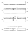
図1に示すように、関連技術の電子部品装置100では、下側に配置されたシリコン基板200の中央部にキャビティCが設けられており、シリコン基板200の周縁にリング状の枠部Fが立設している。
As shown in FIG. 1, in the related-art
シリコン基板200のキャビティCの底部側には、上面から下面まで貫通するスルーホールTHが設けられている。シリコン基板200の両面及びスルーホールTHの内面には絶縁層220が形成され、スルーホールTH内には貫通電極240が充填されている。さらに、シリコン基板200の下面には貫通電極240に接続される配線層300が形成されている。
On the bottom side of the cavity C of the
シリコン基板200のキャビティCの底面中央部には第1接着剤400によって台座500が固定されている。さらに、台座500の上にはMEMS素子600(加速度センサ)の接続電極620が上側を向いた状態で第2接着剤420によってMEMS素子600の背面が固定されている。
A
台座500及び第1、第2接着剤400,420の厚みによって、MEMS素子600の可動部600aがシリコン基板200から離れて配置されている。これによって、MEMS素子600はその可動部600aがフリーな状態となってシリコン基板200に実装されている。
Depending on the thickness of the
MEMS素子600の接続電極620は、ワイヤ620によってシリコン基板200に設けられた貫通電極240の上面に電気的に接続されている。
The
さらに、シリコン基板200の枠部Fにはキャップ700が接合されており、MEMS素子600がキャビティC内に真空状態で気密封止されている。
Further, a
高性能なMEMS素子600の性能を十分に引き出すためには、MEMS素子600が水平度の高い状態で配置されること、及び十分な真空状態で気密封止される必要がある。
In order to sufficiently bring out the performance of the high-
関連技術では、第1接着剤400で固定された台座500の上に第2接着剤420でMEMS素子600を固定するため、第1、第2接着剤400,420のばらつきなどによってMEMS素子600が傾いて配置されやすく、十分な水平度が得られない場合が多い。
In the related art, since the
また、真空雰囲気でMEMS素子600をキャップ700で気密封止する際に、第1、第2接着剤400、420からその成分が揮発するため、キャビティC内で十分な真空度が得られない問題がある。
In addition, when the
以下に説明する実施形態では、上記した不具合を解消することができる。 In the embodiment described below, the above-described problems can be solved.
(第1の実施の形態)
図2〜図8は第1実施形態の電子部品装置の製造方法を示す断面図、図9は同じく電子部品装置を示す断面図である。第1実施形態の電子部品装置の製造方法では、図2(a)に示すように、まず、配線基板を得るための第1シリコンウェハ10を用意する。第1シリコンウェハ10の厚みは600〜700μm程度である。
(First embodiment)
2-8 is sectional drawing which shows the manufacturing method of the electronic component apparatus of 1st Embodiment, FIG. 9 is sectional drawing which similarly shows an electronic component apparatus. In the method of manufacturing the electronic component device according to the first embodiment, as shown in FIG. 2A, first, a first silicon wafer 10 for obtaining a wiring board is prepared. The thickness of the
次いで、図2(b)に示すように、スルーホールが配置される位置に開口部11aが設けられたレジスト11をフォトリソグラフィによって第1シリコンウェハ10の上に形成する。
Next, as shown in FIG. 2B, a
続いて、図2(c)に示すように、レジスト11をマスクにしてその開口部11aを通して異方性ドライエッチング(RIEなど)により第1シリコンウェハ10の上面から厚みの途中までエッチングして穴部10aを形成する。その後に、レジスト11が除去される。
Subsequently, as shown in FIG. 2C, etching is performed from the upper surface of the first silicon wafer 10 to the middle of the thickness by anisotropic dry etching (RIE or the like) through the opening 11a using the
さらに、図2(d)に示すように、第1シリコンウェハ10をその背面側からBG(バックグラインダー)によって研削することにより穴部10aを露出させる。これにより、第1シリコンウェハ10の穴部10aが第1シリコンウェハ10の厚み方向に貫通するスルーホールTHとなる。
Further, as shown in FIG. 2 (d), the
このようにして、厚みが200〜400μmに薄型化された第1シリコンウェハ10にスルーホールTHが設けられた状態となる。スルーホールTHは水平方向の断面が例えば円形状で形成される。
In this way, the through hole TH is provided in the
第1シリコンウェハ10には複数の素子搭載領域Aが画定されており、各素子搭載領域Aに複数のスルーホールTHがそれぞれ配置される。図2(d)には第1シリコンウェハ10内の一つの素子搭載領域Aが示されている。
A plurality of element mounting areas A are defined in the
次いで、図3(a)に示すように、第1シリコンウェハ10を熱酸化することにより、第1シリコンウェハ10の両面及びスルーホールTHの内面にシリコン酸化層からなる絶縁層12を形成する。あるいは、CVD法により第1シリコンウェハ10の全面にシリコン酸化層やシリコン窒化層を形成して絶縁層12としてもよい。
Next, as shown in FIG. 3A, the
さらに、図3(b)に示すように、銅箔などの導電部材15の上に図3(a)の第1シリコンウェハ10を配置する。そして、図3(c)に示すように、導電部材15をめっき給電経路に利用する電解めっきにより第1シリコンウェハ10のスルーホール10aの下部から上部にかけて銅などの金属めっきを施すことにより、貫通電極16を形成する。このとき、貫通電極16は、第1シリコンウェハ10上の絶縁層12から上側に突出して形成される。
Further, as shown in FIG. 3B, the
その後に、図3(d)に示すように、導電部材15が第1シリコンウェハ10から除去される。さらに、第1シリコンウェハ10の上面から突出する貫通電極16を研磨によって除去して第1シリコンウェハ10の上面側を平坦化する。貫通電極16の上面と絶縁層12の上面とが同一面になって平坦化される。
Thereafter, the
次いで、図4(a)に示すように、第1シリコンウェハ10の両面側にスパッタ法によりチタン(Ti)層/銅(Cu)層を順に形成するなどして厚みが0.1μm程度のシード層20aをそれぞれ得る。
Next, as shown in FIG. 4A, a seed having a thickness of about 0.1 μm is formed by sequentially forming a titanium (Ti) layer / copper (Cu) layer on both sides of the
続いて、図4(b)に示すように、第1シリコンウェハ10の下面側のシード層20aの上(図4(b)では下)に、配線層が配置される部分に開口部18aが設けられためっきレジスト18をフォトリソグラフィによって形成する。
Subsequently, as shown in FIG. 4B, an
さらに、第1シリコンウェハ10の上面全体を保護シート(不図示)で保護した状態で、下側のシード層20aをめっき給電経路に利用する電解めっきによりめっきレジスト18の開口部18aに銅などからなる金属めっき層20bを形成する。
Further, with the entire upper surface of the
続いて、めっきレジスト18を除去した後に、金属めっき層20bをマスクにしてシード層20aをエッチングして除去する。
Subsequently, after removing the plating resist 18, the
これにより、図4(c)に示すように、第1シリコンウェハ10の下面にシード層20a及び金属めっき層20bから形成される配線層20が得られる。配線層20は貫通電極16に電気的に接続されて形成される。
Thereby, as shown in FIG. 4C, the
次いで、図4(d)に示すように、第1シリコンウェハ10の下面側に、配線層20の接続部上に開口部22aが設けられたソルダレジスト22を形成する。さらに、配線層20の接続部に無電解めっきによってニッケル(Ni)層/金(Au)層を順に形成するなどしてコンタクト層20xを得る。
Next, as illustrated in FIG. 4D, a solder resist 22 having an opening 22 a on the connection portion of the
続いて、図5(a)に示すように、図4(d)の第1シリコンウェハ10の上面側において、リング状の接合部となる部分に開口部23aが設けられためっきレジスト23をフォトリソグラフィによって形成する。
Subsequently, as shown in FIG. 5A, the plating resist 23 in which the opening 23a is provided in the portion to be the ring-shaped joint on the upper surface side of the
さらに、第1シリコンウェハ10の下面全体を保護シート(不図示)で保護した状態で、シード層20aをめっき給電経路に利用する電解めっきにより、めっきレジスト23の開口部23aに、下から順にCu層/Ni層/Au層を形成して金属部24aを得る。
Further, with the entire lower surface of the
その後に、図5(b)に示すように、めっきレジスト23が除去される。後述するように、金属部24aはキャップを接合するための接合部として機能し、素子形成領域Aを取り囲むようにリング状に配置される。
Thereafter, as shown in FIG. 5B, the plating resist 23 is removed. As will be described later, the
次いで、図5(c)に示すように、貫通電極16に対応するシード層20aの上に開口部25aが設けられためっきレジスト25を形成する。さらに、第1シリコンウェハ10の下面全体を保護シート(不図示)で保護した状態で、シード層20aをめっき給電経路に利用する電解めっきによってめっきレジスト25の開口部25aに金属めっきを施すことにより金属柱32とその上に積層される接合用インジウム(In)層30dとを形成する。
Next, as shown in FIG. 5C, a plating resist 25 having an
図5(c)の部分拡大断面図に示すように、金属柱32は、下から順に、Cu層30a(厚み:50μm)/Ni層30b(厚み:1μm)/Au層30c(厚み:1μm)から形成され、その上に接合用In層30d(厚み:3μm)が積層される。金属柱32は厚み方向においてCu層30aが主体となるように形成される。
As shown in the partially enlarged cross-sectional view of FIG. 5C, the
その後に、めっきレジスト25を除去した後に、金属柱32及び金属部24aをそれぞれマスクにしてシード層20aをエッチングして除去する。
Thereafter, after removing the plating resist 25, the
これにより、図6に示すように、貫通電極16の上に、シード層20a、Cu層30a、Ni層30b、及びAu層30cから形成される電極ポスト30と、電極ポスト30の上端面に設けられた接合用In層30dとを有する電極構造が形成される。電極ポスト30は貫通電極16に電気的に接続されて形成される。
Thus, as shown in FIG. 6, the
電極ポスト30の形状の一例としては、円柱状の電極として形成される。これと同時に、素子形成領域Aを取り囲むようにリング状の接合部24がシード層20a及び金属部24aから形成される。接合部24の配置の一例としては、矩形の枠状に形成される。
An example of the shape of the
接合用In層30dを含めた電極ポスト30の高さは、前述した各層の厚みの例では55.1μm程度に設定されるが、実装する電子部品の特性に合わせて適宜調整される(例えば30〜80μm).後述するように、電極ポスト30上の接合用In層30dには電子部品がフリップチップ接合される。
The height of the
このようにして、電極ポストの上にその金属材料と異なる金属からなる接合用金属層が設けられた電極構造が形成される。本実施形態の電極構造の例では、電極ポスト30はシード層20a、Cu層30a、Ni層30b、及びAu層30cから形成され、その上に電極ポスト30の金属材料と異なる接合用In層30dが形成される。
In this way, an electrode structure is formed in which a bonding metal layer made of a metal different from the metal material is provided on the electrode post. In the example of the electrode structure of this embodiment, the
また、図6の部分拡大平面図に示すように、電極ポスト30の径D2はスルーホールTH(貫通電極16)の径D1より大きく設定され、電極ポスト30がスルーホールTH(貫通電極16)の端部全体を被覆して形成される。例えば、スルーホールTHの径D1は60μmであり、電極ポスト30の径D2は80μmに設定される。この場合、スルーホールTHの外周からの電極ポスト30のかぶり量Lは10μmとなる。
Further, as shown in the partially enlarged plan view of FIG. 6, the diameter D2 of the
後述するように、電極ポスト30に電子部品がフリップチップ接合された後に、真空雰囲気でキャップが接合されて電子部品がキャビティ内に気密封止される。このとき、スルーホールTHの内面(絶縁層12)には電解めっきで形成されたCu層が接触しているため、密着性が十分ではない。
As will be described later, after the electronic component is flip-chip bonded to the
従って、スルーホールTHより電極ポスト30を小さく設定すると、スルーホールTH内の密着性の悪い界面が露出するため、真空漏れが生じて十分な真空度が得られなくなるおそれがある。
Therefore, if the
本実施形態では、スルーホールTHの径より電極ポスト30の径を大きく設定することにより、電極ポスト30の最下のシード層20aでスルーホールTHの端部全体を封止することができる。スパッタ法で形成されたシード層20aは下地(絶縁層12及び貫通電極16)との密着性が良好であるためその界面から真空漏れが生じるおそれはなく、キャビティ内を十分な真空度にすることができる。
In the present embodiment, by setting the diameter of the
図6の例では、第1シリコンウェハ10の複数のスルーホールTH(貫通電極16)の真上に島状に電極ポスト30がそれぞれ配置されている。他の形態として、貫通電極16に接続されて外側に延在する引き出し配線の終端部に電極ポストが配置されるようにしてもよい。この場合も、スルーホールTH(貫通電極16)の真上にそれより大きな引き出し配線の接続パッドが配置されてスルーホールTHが封止される。
In the example of FIG. 6, the electrode posts 30 are arranged in an island shape directly above the plurality of through holes TH (through electrodes 16) of the
次いで、図7(a)に示すように、電子部品としてMEMS素子40を用意する。図7(a)の例では、MEMS素子40として加速度センサが示されている。加速度センサにおいてピエゾ抵抗方式を採用する場合は、センサ素子可動部と固定部をつなぐばね部分に配置されたピエゾ抵抗素子により、加速度によってばね部分に発生した歪みを検出する。あるいは、静電容量検出方式を採用する場合は、センサ素子可動部と固定部の間の容量変化を検出する。
Next, as shown in FIG. 7A, a
図7(a)のMEMS素子40では周縁側に可動部40aが配置されており、中央部に接続電極42が配置されている。MEMS素子40の接続電極42は最外に金(Au)層が形成された構造を有し、全体にわたってAu層から形成してもよく、あるいは、最上層のみがAu層から形成された積層構造であってもよい。
In the
そして、図7(b)に示すようにMEMS素子40の接続電極42を第1シリコンウェハ10に設けられた電極ポスト30上の接合用In層30dにフリップチップ接合する。つまり、第1シリコンウェハ10に設けられた電極ポスト30上の接合用In層30d(図6)にMEMS素子40の接続電極42(Au層)を配置し、200℃の温度で加熱しながらMEMS素子40を下側に加圧する。
Then, as shown in FIG. 7B, the
これにより、電極ポスト30上の接合用In層30dとMEMS素子40の接続電極42のAu層とが反応して合金化し、それらの界面にAu・In合金層31が形成されて、MEMS素子40の接続電極42と電極ポスト30とが接合される。つまり、接合用In層30dと接続電極42の金属材料とによって合金層が形成される。
As a result, the bonding In
なお、上記した形態とは逆に、第1シリコンウェハ10に設けられた電極ポスト30上に接合用Au層を形成し、MEMS素子40の接続電極42の最外にIn層を形成することにより、電極ポスト30とMEMS素子40の接続電極42とがAu・In合金層31によって接合されるようにしてもよい。
Contrary to the above-described embodiment, a bonding Au layer is formed on the
本実施形態では、接着剤を使用することなく、第1シリコンウェハ10に設けられた電極ポスト30にMEMS素子40の接続電極42をAu・In合金層31によって固定する。複数の電極ポスト30はめっきによってそれらの高さが均一になるように形成することが可能である。
In this embodiment, the
従って、接合用In層30dの下の電極ポスト30の金属層が高さの均一なポスト(柱)として機能するため、MEMS素子40を水平度の高い状態で実装することができる。つまり、MEMS素子40を第1シリコンウェハ10の基板面と平行に配置することができる。これにより、高性能なMEMS素子40の性能を十分に引き出すことが可能になる。
Therefore, since the metal layer of the
このとき、電極ポスト30上の接合用In層30dのほとんどがMEMS素子40の接続電極42(金層)と反応してAu・In合金層31となる。この際に、電極ポスト30のAu層30cも反応してAu・In層31の一部となってもよい。接合用In層30dの融点は180〜200℃と比較的低いが、Au・In合金層31となることにより融点が500℃程度まで上昇する。
At this time, most of the bonding In
従って、200℃以上の高温の雰囲気で使用する場合であっても、MEMS素子40と電極ポスト30との電気接続の十分な信頼性が得られる。
Therefore, sufficient reliability of electrical connection between the
なお、上記したMEMS素子40では、周縁側に可動部40aが設けられているが、逆に、中央部に可動部が設けられて周縁側に接続電極が設けられたMEMS素子を使用してもよい。この場合は、前述したように貫通電極16から外側に延在する引き出し配線の終端部に形成された電極ポストにMEMS素子の接続電極が接合される。
In the above-described
または、MEMS素子40の接続電極42の配置に合わせて、貫通電極16と電極ポスト30の配置を変更して形成する。
Alternatively, the arrangement of the through
次いで、図8(a)に示すように、キャップを得るための第2シリコンウェハ50を用意する。第2シリコンウェハ50には複数のキャビティC(凹部)が設けられている。第2シリコンウェハ50には格子状に繋がって配置された突起部50aが形成され、それによって複数のキャビティCが区画されている。突起部50aの形状の一例としては、平面視して矩形の枠状に形成される。
Next, as shown in FIG. 8A, a
そして、第2シリコンウェハ50の突起部50aは、前述した第1シリコンウェハ10に設けられた接合部24に対応する部分に設けられている。また、第2シリコンウェハ50のキャビティCはMEMS素子40が収容される部分に対応して設けられている。
The
第2シリコンウェハ50の突起部50a及びキャビティCは、シリコンウェハの上に所要の開口部を備えたマスクが形成され、その開口部を通してシリコンウェハが異方性ドライエッチングによって加工されて形成される。
The
さらに、第2シリコンウェハ50の突起部50aの先端には最外がIn層からなる接合部50bが形成されている。接合部50bの形成方法としては、まず、第2シリコンウェハ50のキャビティC側の面全体にシード層(Cu層など)を形成した後に、突起部50a上に開口部が設けられためっきレジスト(不図示)を形成する。
Furthermore, a joint 50b whose outermost portion is an In layer is formed at the tip of the
続いて、シード層をめっき給電経路に利用する電解めっきにより、めっきレジストの開口部にIn層を形成する。さらに、めっきレジストを除去した後に、In層をマスクにしてシード層をエッチングする。これにより、第2シリコンウェハ50の突起部50aの先端にシード層及びIn層から形成される接合部50bが得られる。
Subsequently, an In layer is formed in the opening of the plating resist by electrolytic plating using the seed layer as a plating power supply path. Further, after removing the plating resist, the seed layer is etched using the In layer as a mask. Thereby, the
次いで、図8(b)に示すように、第2シリコンウェハ50の接合部50bを第1シリコンウェハ10の接合部24の上に配置し、200℃の温度で加熱しながら第2シリコンウェハ50を下側に加圧する。
Next, as shown in FIG. 8B, the joint 50b of the
これにより、第2シリコンウェハ50の接合部50bの最下のIn層と第1シリコンウェハ10の接合部24の最上のAu層とが反応して合金化し、それらの界面にAu・In合金層51が形成されて両者が接合される。
Thereby, the lowermost In layer of the joint 50b of the
第1シリコンウェハ10と第2シリコンウェハ50との接合は真空雰囲気で行われ、第2シリコンウェハ50のキャビティC内が真空となった状態でMEMS素子40がキャビティC内に収容されて気密封止される。
The bonding of the
なお、上記した形態とは逆に、第1シリコンウェハ10の接合部24の最上にIn層を形成し、第2シリコンウェハ50の接合部50bの最外にAu層を形成することにより、両者がAu・In合金層51によって接合されるようにしてもよい。
Contrary to the above-described embodiment, the In layer is formed on the uppermost part of the
本実施形態では、前述した関連技術と違って接着剤を使用しないため、MEMS素子40がキャビティC内に真空状態で気密封止される際に接着剤の成分が揮発して真空度が低下するおそれがない。このため、所望の真空度でMEMS素子40をキャビティC内に気密封止することができる。
In the present embodiment, unlike the related art described above, no adhesive is used. Therefore, when the
また、前述したように、第1シリコンウェハ10に設けられた電極ポスト30の径はスルーホールTHの径より大きく設定されている。このため、電極ポスト30の最下のシード層20aでスルーホールTHと貫通電極16の間の密着性の悪い界面が封止されるので、スルーホールTHと貫通電極16との界面から真空漏れが起こる恐れがない。
As described above, the diameter of the
従って、MEMS素子40が十分な真空度のキャビティC内に気密封止されるため、高性能なMEMS素子40の性能を十分に引き出すことが可能になる。
Therefore, since the
その後に、図9に示すように、図8(b)の第2シリコンウェハ50及び第1シリコンウェハ10を各素子搭載領域Aが得られるように切断して分割することにより、個々の電子部品装置1を得る。
Thereafter, as shown in FIG. 9, the
図9に示すように、第1実施形態の電子部品装置1では、インターポーザとしてシリコン配線基板5が使用されている。シリコン配線基板5では、シリコン基板10xにスルーホールTHが設けられており、シリコン基板10xの両面及びスルーホールTHの内面に絶縁層12が形成されている。
As shown in FIG. 9, in the
シリコン基板10xのスルーホールTH内には貫通電極16が形成されている。シリコン基板10xの下面には貫通電極16に接続される配線層20が形成されている。また、シリコン基板10xの下面には、配線層20の接続部上に開口部22aが設けられたソルダレジスト22が形成されている。配線層20の接続部にNi/Auめっき層などからなるコンタクト層20xが形成されている。
A through
さらに、シリコン基板10xの上面側には貫通電極16に接続される電極ポスト30が立設して形成されている。電極ポスト30は貫通電極16の真上に配置され、下から順に、シード層20a及び金属柱32が積層されて形成される。
Furthermore, an
このようにして、シリコン配線基板5では、電極ポスト30と配線層20とが貫通電極16を介して相互接続されている。
In this way, in the
図9のシリコン配線基板5においてMEMS素子40が実装される前の配線基板の段階では、電極ポスト30の上にそれと金属材料の異なる接合用In層30d(接合用金属層)(図6)が設けられている。
In the stage of the wiring board before the
さらに、シリコン配線基板5の電極ポスト30にはMEMS素子40の接続電極42がフリップチップ接合されている。シリコン配線基板5の電極ポスト30とMEMS素子40の接続電極42とはAu・In合金層31によって直接接合されている。
Further, the
本実施形態では、MEMS素子40の接続電極42とシリコン配線基板5の電極ポスト30とをAu・In合金層31で接合する形態を例示するが、電極ポスト30の金属材料と異なる金属を含む各種の合金層によって接合されていればよい。
In the present embodiment, an example in which the
本実施形態では、電極ポストとして、シード層20a、Cu層30a、Ni層30b及びAu層30cからなる積層構造の電極ポスト30(図7(b))が例示され、電極ポスト30の金属材料と異なる金属を含む合金層として、Au・In合金層31が例示されている。
In the present embodiment, as the electrode post, the electrode post 30 (FIG. 7B) having a laminated structure including the
また、シリコン配線基板5に実装されたMEMS素子40がキャップシリコン基板50xのキャビティCに収容されるようにしてシリコン配線基板5の上にキャップシリコン基板50xが配置されている。
Further, the
シリコン配線基板5の接合部24に、キャップシリコン基板50xの突起部50aに設けられた接合部50bがAu・In合金層51によって接合されている。シリコン配線基板5のリング状の接合部24にキャップシリコン基板50xのリング状の接合部50bが接合されており、キャビティC内が真空状態で気密封止されている。
A
このようにして、シリコン配線基板5の電極ポスト30に実装されたMEMS素子40は、キャップシリコン基板50xのキャビティC内に収容されて真空状態で気密封止されている。
In this way, the
第1実施形態の電子部品装置1では、前述したように。接着剤を使用することなく、MEMS素子40がAu・In合金層31でシリコン配線基板5の電極ポスト30に接合されるので、MEMS素子40を高い精度の水平度で実装することができる。
As described above, in the
また、前述したように、MEMS素子40を実装する際に接着剤を使用しないことから揮発成分がないので、MEMS素子40をキャビティC内に真空状態で気密封止する際に真空度が低下するおそれもない。
Further, as described above, since no adhesive is used when the
しかも、前述したように、電極ポスト30でスルーホールTHと貫通電極16の間の密着性の悪い界面が封止されるので、スルーホールTHと貫通電極16との界面から真空漏れが起こるおそれがない。
In addition, as described above, the
このように、MEMS素子 40が高い精度の水平度で実装されると共に、十分な真空度のキャビティC内に気密封止されるため、高性能なMEMS素子40の性能を十分に引き出すことが可能になる。
Thus, since the
また、本実施形態では、関連技術のようなMEMS素子40をワイヤで接続するのではなく、MEMS素子40の接続電極42を電極ポスト30にフリップチップ接合で直接接合している。このため、ワイヤのループの高さを考慮する必要がないので、電子部品装置の薄型化を図ることができる。また、MEMS素子40の外側にワイヤ接続用の電極を配置する必要がないので、実装面積を縮小することができ、電子部品装置の小型化を図ることができる。
In the present embodiment, the
また、Au・In合金層31の融点は500℃程度であるため、200℃以上の高温の雰囲気で使用する場合であっても、MEMS素子40と電極ポスト30との電気接続の十分な信頼性が得られる。
Further, since the melting point of the Au / In
図10には、第1実施形態の第1変形例の電子部品装置1aが示されている。図10に示すように、第1変形例の電子部品装置1aでは、MEMS素子40の代わりに、半導体素子60(LSIチップ)の接続電極62がシリコン配線基板5の電極ポスト30にAu・In合金層31によってフリップチップ接合されている。その他の構成要素は図9と同一である。
FIG. 10 shows an
特に半導体素子60として発熱量が大きなロジックLSI(CPUなど)を使用する場合、通常のフリップチップ接合では、熱応力の発生により接続部の周りにクラックが発生するなどして接合破壊が発生することがある。
In particular, when a logic LSI (CPU or the like) that generates a large amount of heat is used as the
図10に示すように、半導体素子60をシリコン配線基板5から上側に離して実装することにより、柔かなCu柱を含む電極ポスト30で応力が緩和されるため、半導体素子60の接合破壊の発生を防止することができる。
As shown in FIG. 10, by mounting the
なお、電子部品として半導体素子60を使用する場合は、必ずしもキャップシリコン基板50xで気密封止する必要はない。
When the
図11には、第1実施形態の第2変形例の電子部品装置1bが示されている。図11に示すように、第2変形例の電子部品装置1bでは、キャップシリコン基板50xの代わりに、キャップガラス基板52が使用される。
FIG. 11 shows an
キャップガラス基板52の突起状接合部52aがシリコン配線基板5の周縁部のシリコン接合部10yに陽極接合によって接合されている。キャップガラス基板52のキャビティC内にMEMS素子40が真空状態で気密封止されている。
The protruding joint 52 a of the
キャビティCが設けられたガラスキャップ基板52は、ガラスウェハの上に所要の開口部を備えたマスクが形成され、その開口部に露出するガラスウェハの部分がサンドブラスト法によって加工されて形成される。あるいは、所要の型に溶融したガラスを流し込むことによって作成してもよい。
The
第2変形例の電子部品装置1bの製造する際には、前述した図5〜図6の工程で、接合部24の形成を省略し、第1シリコンウェハ10の各素子搭載領域Aの周縁部の絶縁層12をエッチングして除去してリング状にシリコン接合部10yを露出させる。
When manufacturing the
そして、キャップガラス基板52を得るためのガラスウェハの突起状接合部52aを第1シリコンウェハ10のシリコン接合部10yに陽極接合によって接合する。陽極接合の条件としては、例えば、第1シリコンウェハ10及びガラスウェハを300〜400℃に加熱した状態で、両者の間に500V〜1KVの電圧を印加する。
Then, the glass wafer protruding joint 52 a for obtaining the
これによって、第1シリコンウェハ10とガラスウェハとの間に大きな静電引力が発生し、それらの界面で化学結合することによってガラスウェハの突起状接合部52aが第1シリコンウェハ10のシリコン接合部10yに接合される。
As a result, a large electrostatic attractive force is generated between the
また、陽極接合時においても、真空雰囲気で行われ、MEMS素子40がガラスウェハのキャビティC内に真空状態で収容されて気密封止される。
In addition, the anodic bonding is performed in a vacuum atmosphere, and the
その後に、ガラスウェハ及び第1シリコンウェハ10が切断されて、シリコン配線基板5の上にキャップガラス基板52が接合された個々の電子部品装置が得られる。
Thereafter, the glass wafer and the
あるいは、特に図示しないが、シリコン配線基板5の代わりにガラス配線基板を使用してもよい。ガラス配線基板を使用する場合は、ガラスウェハをレーザやドリルなどで加工することにより、シリコン配線基板5と同様な構造のガラス配線基板を得ることができる。ガラス配線基板を使用する場合は、絶縁層12の形成(図3(a))を省略することができる。
Alternatively, although not particularly illustrated, a glass wiring board may be used instead of the
または、ガラス配線基板の上にキャップシリコン基板を接合してもよいし、ガラス配線基板の上にキャップガラス基板を接合してもよい。 Alternatively, a cap silicon substrate may be bonded onto the glass wiring substrate, or a cap glass substrate may be bonded onto the glass wiring substrate.
(第2の実施の形態)
図12は第2実施形態の電子部品装置を示す断面図である。
(Second Embodiment)
FIG. 12 is a cross-sectional view showing the electronic component device of the second embodiment.
第2実施形態が第1実施形態と異なる点は、シリコン配線基板側にキャビティを形成し、平板状のキャップシリコン基板でキャップすることにある。第2実施形態では、第1実施形態と同一要素については同一符号を付してその詳しい説明を省略する。 The second embodiment differs from the first embodiment in that a cavity is formed on the silicon wiring substrate side and capped with a flat cap silicon substrate. In the second embodiment, the same elements as those in the first embodiment are denoted by the same reference numerals, and detailed description thereof is omitted.
図12に示すように、第2実施形態の電子部品装置2では、シリコン配線基板5の中央部にキャビティC(凹部)が設けられており、周縁部にリング状の枠部Fが配置されている。そして、第1実施形態と同様に、キャビティCの底部にシリコン基板を貫通する貫通電極16が設けられており、貫通電極16の上に電極ポスト30が立設して形成されている。さらに、第1実施形態と同様に、電極ポスト30にMEMS素子40の接続電極42がAu・In合金層31によって接続されている。
As shown in FIG. 12, in the electronic component device 2 of the second embodiment, a cavity C (concave portion) is provided in the central portion of the
また、シリコン配線基板5の枠部Fには平板状のキャップシリコン基板50xが配置されている。第1実施形態と同様に、キャップシリコン基板50xの接合部50bとシリコン配線基板5の枠部F上の接合部24とがAu・In合金層51によって接合されている
図12のキャビティCが設けられたシリコン配線基板5は、前述した図2(c)の工程の後に、第1シリコンウェハ10の背面側にキャビティCが配置される部分に開口部が設けられたマスクを配置し、その開口部を通して穴部10aと連通するまでシリコンウェハをハーフエッチングすることに基づいて得られる。
A flat
第2実施形態の電子部品装置2は第1実施形態の電子部品装置1と同様な効果を奏する。
The electronic component device 2 of the second embodiment has the same effects as the
図13には第2実施形態の第1変形例の電子部品装置2aが示されている。
FIG. 13 shows an
図13に示すように、第1実施形態の第1変形例(図10)と同様に、前述した図12において、MEMS素子40の代わりにロジックLSIなどの半導体素子60を同様に実装してよい。
As shown in FIG. 13, similarly to the first modified example (FIG. 10) of the first embodiment, in FIG. 12 described above, a
また、図14には、第2実施形態の第2変形例の電子部品装置2bが示されている。
FIG. 14 shows an
図14に示すように、第1実施形態の第2変形例(図11)と同様に、前述した図12において、キャップシリコン基板50xの代わり、キャップガラス基板52をシリコン配線基板5の枠部Fの上面のシリコン接合部10yに陽極接合してもよい。
As shown in FIG. 14, the
1,1a,1b,2,2a,2b…電子部品装置、10…第1シリコンウェハ、10x…シリコン基板、10y…シリコン接合部、11…レジスト、11a,22a,23a,25a…開口部、10a…穴部、12…絶縁層、16…貫通電極、20…配線層、20a…シード層、20b…金属めっき層、20x…コンタクト層、22…ソルダレジスト、23,25…めっきレジスト、24,50b…接合部、24a…金属部、30…電極ポスト、30a…Cu層、30b…Ni層、30c…Au層、30d…接合用In層、31,51…Au・In合金層、32…金属柱、40…MEMS素子、40a…可動部、42,62…接続電極、50…第2シリコンウェハ、50a…突起部、50x…キャップシリコン基板、52…キャップガラス基板、52a…突起状接合部、60…半導体素子、A…素子搭載領域、C…キャビティ、F…枠部、TH…スルーホール。
DESCRIPTION OF
Claims (14)
前記基板の上に立設する金属材料からなる電解めっきで形成された柱状の電極ポストと、
周縁部に可動部を備え、中央部に複数の接続電極を備えたMEMS素子であって、前記MEMS素子の可動部が前記基板から離れた状態で、前記MEMS素子の複数の接続電極が、対応する複数の前記電極ポストの先端に接合された前記MEMS素子とを有し、
前記電極ポストの高さは、前記MEMS素子の接続電極の厚みより高く設定され、かつ、
前記MEMS素子の接続電極と前記電極ポストとは、前記電極ポストの金属材料と異なる金属を含む合金層によって接合されていることを特徴とする電子部品装置。 A substrate,
Columnar electrode posts formed by electrolytic plating made of a metal material standing on the substrate,
A movable portion to the peripheral portion, a MEMS device having a plurality of connection electrodes in the center, in a state in which the movable portion of the MEMS device is separated from the substrate, a plurality of connecting electrodes of the MEMS element, the corresponding A plurality of the MEMS elements bonded to the tips of the electrode posts,
The height of the electrode post is set higher than the thickness of the connection electrode of the MEMS element, and
The connection part of the said MEMS element and the said electrode post are joined by the alloy layer containing the metal different from the metal material of the said electrode post, The electronic component apparatus characterized by the above-mentioned.
周縁部に可動部を備え、中央部に複数の接続電極を備えたMEMS素子を用意し、前記MEMS素子の複数の接続電極を、対応する複数の前記電極構造に接続する工程とを有し、
前記電極ポストの高さは、前記MEMS素子の接続電極の厚みより高く設定され、かつ、
前記MEMS素子の可動部が前記基板から離れた状態で、前記MEMS素子の接続電極が、前記接合用金属層と前記接続電極との合金層によって前記電極ポストの先端に接合されることを特徴とする電子部品装置の製造方法。 An electrode structure having a columnar electrode post formed by electrolytic plating made of a metal material and a bonding metal layer made of a metal different from the metal material is provided on the tip of the electrode post on a substrate. And a process of
Preparing a MEMS element including a movable part at a peripheral part and a plurality of connection electrodes at a central part, and connecting a plurality of connection electrodes of the MEMS element to a corresponding plurality of the electrode structures;
The height of the electrode post is set higher than the thickness of the connection electrode of the MEMS element, and
The connection electrode of the MEMS element is bonded to the tip of the electrode post by an alloy layer of the bonding metal layer and the connection electrode in a state where the movable portion of the MEMS element is separated from the substrate. A method for manufacturing an electronic component device.
前記基板に厚み方向に貫通する貫通電極が設けられており、前記電極ポストは前記貫通電極に接続されることを特徴とする請求項8又は9に記載の電子部品実装構造の製造方法。 In the step of forming the electrode post,
10. The method of manufacturing an electronic component mounting structure according to claim 8 , wherein a through electrode penetrating in the thickness direction is provided on the substrate, and the electrode post is connected to the through electrode.
前記基板の上にキャップを設ける工程をさらに有し、前記MEMS素子は前記基板と前記キャップとの間のキャビティに気密封止されることを特徴とする請求項8乃至10のいずれか一項に記載の電子部品装置の製造方法。 After the step of bonding the MEMS element to the electrode post,
11. The method according to claim 8 , further comprising a step of providing a cap on the substrate, wherein the MEMS element is hermetically sealed in a cavity between the substrate and the cap. The manufacturing method of the electronic component apparatus of description.
Priority Applications (2)
| Application Number | Priority Date | Filing Date | Title |
|---|---|---|---|
| JP2010229309A JP5615122B2 (en) | 2010-10-12 | 2010-10-12 | Electronic component device and manufacturing method thereof |
| US13/221,064 US8878357B2 (en) | 2010-10-12 | 2011-08-30 | Electronic component device, method of manufacturing the same and wiring substrate |
Applications Claiming Priority (1)
| Application Number | Priority Date | Filing Date | Title |
|---|---|---|---|
| JP2010229309A JP5615122B2 (en) | 2010-10-12 | 2010-10-12 | Electronic component device and manufacturing method thereof |
Publications (3)
| Publication Number | Publication Date |
|---|---|
| JP2012084681A JP2012084681A (en) | 2012-04-26 |
| JP2012084681A5 JP2012084681A5 (en) | 2013-08-15 |
| JP5615122B2 true JP5615122B2 (en) | 2014-10-29 |
Family
ID=45924492
Family Applications (1)
| Application Number | Title | Priority Date | Filing Date |
|---|---|---|---|
| JP2010229309A Active JP5615122B2 (en) | 2010-10-12 | 2010-10-12 | Electronic component device and manufacturing method thereof |
Country Status (2)
| Country | Link |
|---|---|
| US (1) | US8878357B2 (en) |
| JP (1) | JP5615122B2 (en) |
Families Citing this family (8)
| Publication number | Priority date | Publication date | Assignee | Title |
|---|---|---|---|---|
| US20150191349A1 (en) * | 2012-07-11 | 2015-07-09 | Hewlett-Packard Development Company, L.P. | Semiconductor secured to substrate via hole in substrate |
| BR112015002306A2 (en) | 2012-07-31 | 2017-07-04 | Hewlett Packard Development Co | device, system, and method for mounting a device |
| JP6533066B2 (en) * | 2015-02-18 | 2019-06-19 | ローム株式会社 | Electronic device |
| JP6852569B2 (en) * | 2017-05-30 | 2021-03-31 | セイコーエプソン株式会社 | MEMS elements, electronics and mobiles |
| JP6635605B2 (en) * | 2017-10-11 | 2020-01-29 | 国立研究開発法人理化学研究所 | Current introduction terminal, pressure holding device and X-ray imaging device having the same |
| CN114449729B (en) * | 2020-11-06 | 2023-11-10 | 中移物联网有限公司 | Main board protection structure and assembly method thereof |
| TWI753645B (en) * | 2020-11-12 | 2022-01-21 | 錼創顯示科技股份有限公司 | Micro led display and repair method thereof |
| WO2023080375A1 (en) * | 2021-11-02 | 2023-05-11 | 울산과학기술원 | Through-silicon via suitable for mems manufacturing process comprising high-temperature process, and manufacturing method therefor |
Family Cites Families (6)
| Publication number | Priority date | Publication date | Assignee | Title |
|---|---|---|---|---|
| JP2006100552A (en) | 2004-09-29 | 2006-04-13 | Rohm Co Ltd | Wiring board and semiconductor device |
| JP2006179667A (en) | 2004-12-22 | 2006-07-06 | Oki Electric Ind Co Ltd | Package for semiconductor device |
| KR100833508B1 (en) * | 2006-12-07 | 2008-05-29 | 한국전자통신연구원 | Mems package and package method thereof |
| JP2008192833A (en) * | 2007-02-05 | 2008-08-21 | Shinko Electric Ind Co Ltd | Manufacturing method of semiconductor device |
| JP5318685B2 (en) * | 2008-09-26 | 2013-10-16 | セイコーインスツル株式会社 | Electronic component and manufacturing method thereof |
| JP5139347B2 (en) * | 2009-02-18 | 2013-02-06 | 新光電気工業株式会社 | Electronic component device and manufacturing method thereof |
-
2010
- 2010-10-12 JP JP2010229309A patent/JP5615122B2/en active Active
-
2011
- 2011-08-30 US US13/221,064 patent/US8878357B2/en active Active
Also Published As
| Publication number | Publication date |
|---|---|
| JP2012084681A (en) | 2012-04-26 |
| US8878357B2 (en) | 2014-11-04 |
| US20120086116A1 (en) | 2012-04-12 |
Similar Documents
| Publication | Publication Date | Title |
|---|---|---|
| JP5615122B2 (en) | Electronic component device and manufacturing method thereof | |
| JP5026038B2 (en) | Electronic component equipment | |
| US6528344B2 (en) | Chip scale surface-mountable packaging method for electronic and MEMS devices | |
| JP5139347B2 (en) | Electronic component device and manufacturing method thereof | |
| EP2121511B1 (en) | Method of packaging an electronic or micromechanical component | |
| US20040259325A1 (en) | Wafer level chip scale hermetic package | |
| US9540228B2 (en) | MEMS-CMOS device that minimizes outgassing and methods of manufacture | |
| JP4732824B2 (en) | Cap wafer with cavity, semiconductor package using the same, and cap wafer manufacturing method | |
| US8154115B1 (en) | Package structure having MEMS element and fabrication method thereof | |
| TWI431732B (en) | Semiconductor package and manufacturing method thereof | |
| US20160185593A1 (en) | Wafer level package for a mems sensor device and corresponding manufacturing process | |
| TWI455265B (en) | A package structure having a micro-electromechanical element and a manufacturing method thereof | |
| JP2006156436A (en) | Semiconductor device and its manufacturing method | |
| TW201631715A (en) | Wiring substrate, method of manufacturing the same and electronic component device | |
| TW201349414A (en) | Package structure having MEMS component and fabrication method thereof | |
| TWI388038B (en) | Structure and fabrication method of a sensing device | |
| US8039967B2 (en) | Wiring substrate with a wire terminal | |
| JP5248179B2 (en) | Manufacturing method of electronic device | |
| TW201606948A (en) | Chip package and method thereof | |
| JP2007227596A (en) | Semiconductor module and its manufacturing method | |
| TWI522308B (en) | Mems package structure and method of forming the same | |
| JP5112659B2 (en) | Acceleration sensor, sensor chip and manufacturing method thereof | |
| JP2014086963A (en) | Package and method of manufacturing package | |
| JP2007335642A (en) | Package substrate | |
| JP2011106841A (en) | Sensor unit and method for manufacturing the same |
Legal Events
| Date | Code | Title | Description |
|---|---|---|---|
| A521 | Request for written amendment filed |
Free format text: JAPANESE INTERMEDIATE CODE: A523 Effective date: 20130626 |
|
| A621 | Written request for application examination |
Free format text: JAPANESE INTERMEDIATE CODE: A621 Effective date: 20130626 |
|
| A977 | Report on retrieval |
Free format text: JAPANESE INTERMEDIATE CODE: A971007 Effective date: 20140116 |
|
| A131 | Notification of reasons for refusal |
Free format text: JAPANESE INTERMEDIATE CODE: A131 Effective date: 20140121 |
|
| A521 | Request for written amendment filed |
Free format text: JAPANESE INTERMEDIATE CODE: A523 Effective date: 20140310 |
|
| TRDD | Decision of grant or rejection written | ||
| A01 | Written decision to grant a patent or to grant a registration (utility model) |
Free format text: JAPANESE INTERMEDIATE CODE: A01 Effective date: 20140902 |
|
| A61 | First payment of annual fees (during grant procedure) |
Free format text: JAPANESE INTERMEDIATE CODE: A61 Effective date: 20140909 |
|
| R150 | Certificate of patent or registration of utility model |
Ref document number: 5615122 Country of ref document: JP Free format text: JAPANESE INTERMEDIATE CODE: R150 |