JP5602761B2 - 分離した微細構造を有する微小電気機械システムデバイス及びその製造方法 - Google Patents
分離した微細構造を有する微小電気機械システムデバイス及びその製造方法 Download PDFInfo
- Publication number
- JP5602761B2 JP5602761B2 JP2011542203A JP2011542203A JP5602761B2 JP 5602761 B2 JP5602761 B2 JP 5602761B2 JP 2011542203 A JP2011542203 A JP 2011542203A JP 2011542203 A JP2011542203 A JP 2011542203A JP 5602761 B2 JP5602761 B2 JP 5602761B2
- Authority
- JP
- Japan
- Prior art keywords
- layer
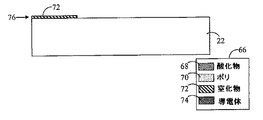
- isolation trench
- nitride
- polysilicon structure
- sacrificial
- Prior art date
- Legal status (The legal status is an assumption and is not a legal conclusion. Google has not performed a legal analysis and makes no representation as to the accuracy of the status listed.)
- Expired - Fee Related
Links
Images


Classifications
-
- B—PERFORMING OPERATIONS; TRANSPORTING
- B81—MICROSTRUCTURAL TECHNOLOGY
- B81C—PROCESSES OR APPARATUS SPECIALLY ADAPTED FOR THE MANUFACTURE OR TREATMENT OF MICROSTRUCTURAL DEVICES OR SYSTEMS
- B81C1/00—Manufacture or treatment of devices or systems in or on a substrate
- B81C1/00642—Manufacture or treatment of devices or systems in or on a substrate for improving the physical properties of a device
- B81C1/00698—Electrical characteristics, e.g. by doping materials
Landscapes
- Engineering & Computer Science (AREA)
- Manufacturing & Machinery (AREA)
- Microelectronics & Electronic Packaging (AREA)
- Micromachines (AREA)
- Pressure Sensors (AREA)
Applications Claiming Priority (3)
| Application Number | Priority Date | Filing Date | Title |
|---|---|---|---|
| US12/340,202 US7943525B2 (en) | 2008-12-19 | 2008-12-19 | Method of producing microelectromechanical device with isolated microstructures |
| US12/340,202 | 2008-12-19 | ||
| PCT/US2009/065905 WO2010080229A1 (en) | 2008-12-19 | 2009-11-25 | Microelectromechanical device with isolated microstructures and method of producing same |
Publications (3)
| Publication Number | Publication Date |
|---|---|
| JP2012512754A JP2012512754A (ja) | 2012-06-07 |
| JP2012512754A5 JP2012512754A5 (enExample) | 2013-01-17 |
| JP5602761B2 true JP5602761B2 (ja) | 2014-10-08 |
Family
ID=42264793
Family Applications (1)
| Application Number | Title | Priority Date | Filing Date |
|---|---|---|---|
| JP2011542203A Expired - Fee Related JP5602761B2 (ja) | 2008-12-19 | 2009-11-25 | 分離した微細構造を有する微小電気機械システムデバイス及びその製造方法 |
Country Status (5)
| Country | Link |
|---|---|
| US (1) | US7943525B2 (enExample) |
| JP (1) | JP5602761B2 (enExample) |
| CN (1) | CN102257609B (enExample) |
| TW (1) | TW201034933A (enExample) |
| WO (1) | WO2010080229A1 (enExample) |
Families Citing this family (23)
| Publication number | Priority date | Publication date | Assignee | Title |
|---|---|---|---|---|
| US20100289065A1 (en) * | 2009-05-12 | 2010-11-18 | Pixart Imaging Incorporation | Mems integrated chip with cross-area interconnection |
| TW201109267A (en) * | 2009-09-08 | 2011-03-16 | Jung-Tang Huang | A general strength and sensitivity enhancement method for micromachined devices |
| TWI388496B (zh) * | 2010-01-12 | 2013-03-11 | Maxchip Electronics Corp | 微機電系統結構及其製造方法 |
| EP2426083A3 (en) * | 2010-09-03 | 2013-11-13 | Domintech Co., LTD. | Mems sensor package |
| CN108470679B (zh) * | 2011-01-25 | 2022-03-29 | Ev 集团 E·索尔纳有限责任公司 | 用于永久接合晶片的方法 |
| CN102183677B (zh) * | 2011-03-15 | 2012-08-08 | 迈尔森电子(天津)有限公司 | 集成惯性传感器与压力传感器及其形成方法 |
| US8673756B2 (en) * | 2011-04-14 | 2014-03-18 | Robert Bosch Gmbh | Out-of-plane spacer defined electrode |
| US8610222B2 (en) | 2011-04-18 | 2013-12-17 | Freescale Semiconductor, Inc. | MEMS device with central anchor for stress isolation |
| US8846129B2 (en) * | 2012-02-13 | 2014-09-30 | Taiwan Semiconductor Manufacturing Company, Ltd. | Biological sensing structures and methods of forming the same |
| US8828772B2 (en) * | 2012-03-05 | 2014-09-09 | Taiwan Semiconductor Manufacturing Co., Ltd. | High aspect ratio MEMS devices and methods for forming the same |
| US9469522B2 (en) * | 2013-03-15 | 2016-10-18 | Robert Bosch Gmbh | Epi-poly etch stop for out of plane spacer defined electrode |
| US9079763B2 (en) | 2013-04-22 | 2015-07-14 | Freescale Semiconductor, Inc. | MEMS device with stress isolation and method of fabrication |
| US9034679B2 (en) | 2013-06-25 | 2015-05-19 | Freescale Semiconductor, Inc. | Method for fabricating multiple types of MEMS devices |
| DE102014202820A1 (de) * | 2014-02-17 | 2015-08-20 | Robert Bosch Gmbh | Schichtenanordnung für ein mikromechanisches Bauelement |
| US9617142B1 (en) * | 2015-09-30 | 2017-04-11 | Mems Drive, Inc. | MEMS grid for manipulating structural parameters of MEMS devices |
| EP3153851B1 (en) | 2015-10-06 | 2024-05-01 | Carrier Corporation | Mems die with sensing structures |
| CN105890827B (zh) * | 2016-01-18 | 2019-05-21 | 广东合微集成电路技术有限公司 | 一种电容式压力传感器及其制造方法 |
| US9950920B2 (en) * | 2016-01-22 | 2018-04-24 | United Microelectronics Corp. | Micro-electro-mechanical system structure and method for forming the same |
| KR102088584B1 (ko) * | 2018-11-28 | 2020-03-12 | 한국과학기술원 | Mems 멤브레인 구조체 및 그 제조방법 |
| DE102020202262A1 (de) * | 2020-02-21 | 2021-08-26 | Robert Bosch Gesellschaft mit beschränkter Haftung | Verfahren zur Herstellung einer nanoskaligen Kanalstruktur |
| IT202000011755A1 (it) * | 2020-05-20 | 2021-11-20 | St Microelectronics Srl | Procedimento di fabbricazione di un dispositivo micro-elettro-meccanico, in particolare sensore di movimento con comando/rilevazione di tipo capacitivo, e relativo dispositivo mems |
| CN113387319B (zh) * | 2021-06-11 | 2023-07-14 | 中国兵器工业集团第二一四研究所苏州研发中心 | 基于多通孔硅基板的mems芯片封装结构及其制备方法 |
| CN116902904A (zh) * | 2023-07-14 | 2023-10-20 | 绍兴中芯集成电路制造股份有限公司 | 一种mems器件、mems器件的制备方法和电子装置 |
Family Cites Families (16)
| Publication number | Priority date | Publication date | Assignee | Title |
|---|---|---|---|---|
| JP3367113B2 (ja) * | 1992-04-27 | 2003-01-14 | 株式会社デンソー | 加速度センサ |
| US6199874B1 (en) * | 1993-05-26 | 2001-03-13 | Cornell Research Foundation Inc. | Microelectromechanical accelerometer for automotive applications |
| US5580815A (en) * | 1993-08-12 | 1996-12-03 | Motorola Inc. | Process for forming field isolation and a structure over a semiconductor substrate |
| US6121552A (en) * | 1997-06-13 | 2000-09-19 | The Regents Of The University Of Caliofornia | Microfabricated high aspect ratio device with an electrical isolation trench |
| DE69942486D1 (de) * | 1998-01-15 | 2010-07-22 | Cornell Res Foundation Inc | Grabenisolation für mikromechanische bauelemente |
| JP4214584B2 (ja) * | 1998-11-27 | 2009-01-28 | 株式会社デンソー | 半導体力学量センサおよびその製造方法 |
| US6395644B1 (en) * | 2000-01-18 | 2002-05-28 | Advanced Micro Devices, Inc. | Process for fabricating a semiconductor device using a silicon-rich silicon nitride ARC |
| DE10065013B4 (de) * | 2000-12-23 | 2009-12-24 | Robert Bosch Gmbh | Verfahren zum Herstellen eines mikromechanischen Bauelements |
| KR100443126B1 (ko) * | 2002-08-19 | 2004-08-04 | 삼성전자주식회사 | 트렌치 구조물 및 이의 형성 방법 |
| US6747338B1 (en) * | 2002-11-27 | 2004-06-08 | Analog Devices, Inc. | Composite dielectric with improved etch selectivity for high voltage MEMS structures |
| US6770506B2 (en) * | 2002-12-23 | 2004-08-03 | Motorola, Inc. | Release etch method for micromachined sensors |
| US6936491B2 (en) * | 2003-06-04 | 2005-08-30 | Robert Bosch Gmbh | Method of fabricating microelectromechanical systems and devices having trench isolated contacts |
| US20060148133A1 (en) * | 2005-01-03 | 2006-07-06 | Analog Devices, Inc. | Method of forming a MEMS device |
| US7372617B2 (en) * | 2005-07-06 | 2008-05-13 | Peter Enoksson | Hidden hinge MEMS device |
| JP2008080444A (ja) * | 2006-09-27 | 2008-04-10 | Toshiba Corp | Mems素子製造方法およびmems素子 |
| DE102006052630A1 (de) * | 2006-10-19 | 2008-04-24 | Robert Bosch Gmbh | Mikromechanisches Bauelement mit monolithisch integrierter Schaltung und Verfahren zur Herstellung eines Bauelements |
-
2008
- 2008-12-19 US US12/340,202 patent/US7943525B2/en not_active Expired - Fee Related
-
2009
- 2009-11-25 WO PCT/US2009/065905 patent/WO2010080229A1/en not_active Ceased
- 2009-11-25 CN CN200980150738.3A patent/CN102257609B/zh not_active Expired - Fee Related
- 2009-11-25 JP JP2011542203A patent/JP5602761B2/ja not_active Expired - Fee Related
- 2009-12-02 TW TW098141176A patent/TW201034933A/zh unknown
Also Published As
| Publication number | Publication date |
|---|---|
| TW201034933A (en) | 2010-10-01 |
| JP2012512754A (ja) | 2012-06-07 |
| WO2010080229A1 (en) | 2010-07-15 |
| US7943525B2 (en) | 2011-05-17 |
| CN102257609B (zh) | 2014-02-12 |
| CN102257609A (zh) | 2011-11-23 |
| US20100155861A1 (en) | 2010-06-24 |
Similar Documents
| Publication | Publication Date | Title |
|---|---|---|
| JP5602761B2 (ja) | 分離した微細構造を有する微小電気機械システムデバイス及びその製造方法 | |
| US8426934B2 (en) | Micro-electro-mechanical system device and method for making same | |
| US8227286B2 (en) | Single crystal silicon sensor with additional layer and method of producing the same | |
| KR101710826B1 (ko) | 반도체 디바이스의 형성 방법 | |
| US7932118B2 (en) | Method of producing mechanical components of MEMS or NEMS structures made of monocrystalline silicon | |
| EP2023151B1 (en) | Sensor with position-indepedent drive electrodes in multi-layer silicon on insulator substrate | |
| US8742595B1 (en) | MEMS devices and methods of forming same | |
| KR100373739B1 (ko) | 단결정 실리콘 웨이퍼 한 장를 이용한 정전형 수직구동기의 제조 방법 | |
| US7618837B2 (en) | Method for fabricating high aspect ratio MEMS device with integrated circuit on the same substrate using post-CMOS process | |
| CN113735055A (zh) | 一种mems器件制造方法及mems器件 | |
| US20020126455A1 (en) | Tiled microelectromechanical device modules and fabrication methods | |
| KR100817813B1 (ko) | 실리콘 기판 상에 상이한 수직 단차를 갖는 미세구조물의제조 방법 | |
| WO2010107618A2 (en) | Method of accurately spacing z-axis electrode | |
| CN112875642A (zh) | Mems器件及其制造方法 | |
| TWI506694B (zh) | 半導體裝置及形成半導體裝置之方法 | |
| JP4857718B2 (ja) | マイクロマシン混載の電子回路装置、およびマイクロマシン混載の電子回路装置の製造方法 | |
| KR100643402B1 (ko) | 마이크로 센서의 부양체 및 그 제조방법 | |
| KR100701151B1 (ko) | 미세기전집적시스템용 부양 구조물 제조 방법 | |
| CN121672404A (zh) | 一种微电子机械传感器及其制备方法 |
Legal Events
| Date | Code | Title | Description |
|---|---|---|---|
| RD04 | Notification of resignation of power of attorney |
Free format text: JAPANESE INTERMEDIATE CODE: A7424 Effective date: 20120227 |
|
| A521 | Request for written amendment filed |
Free format text: JAPANESE INTERMEDIATE CODE: A523 Effective date: 20121122 |
|
| A621 | Written request for application examination |
Free format text: JAPANESE INTERMEDIATE CODE: A621 Effective date: 20121122 |
|
| A131 | Notification of reasons for refusal |
Free format text: JAPANESE INTERMEDIATE CODE: A131 Effective date: 20140107 |
|
| A521 | Request for written amendment filed |
Free format text: JAPANESE INTERMEDIATE CODE: A523 Effective date: 20140331 |
|
| TRDD | Decision of grant or rejection written | ||
| A01 | Written decision to grant a patent or to grant a registration (utility model) |
Free format text: JAPANESE INTERMEDIATE CODE: A01 Effective date: 20140722 |
|
| A61 | First payment of annual fees (during grant procedure) |
Free format text: JAPANESE INTERMEDIATE CODE: A61 Effective date: 20140820 |
|
| R150 | Certificate of patent or registration of utility model |
Ref document number: 5602761 Country of ref document: JP Free format text: JAPANESE INTERMEDIATE CODE: R150 |
|
| R250 | Receipt of annual fees |
Free format text: JAPANESE INTERMEDIATE CODE: R250 |
|
| LAPS | Cancellation because of no payment of annual fees |