JP5578045B2 - Detection apparatus, sensor device, and electronic apparatus - Google Patents
Detection apparatus, sensor device, and electronic apparatus Download PDFInfo
- Publication number
- JP5578045B2 JP5578045B2 JP2010260001A JP2010260001A JP5578045B2 JP 5578045 B2 JP5578045 B2 JP 5578045B2 JP 2010260001 A JP2010260001 A JP 2010260001A JP 2010260001 A JP2010260001 A JP 2010260001A JP 5578045 B2 JP5578045 B2 JP 5578045B2
- Authority
- JP
- Japan
- Prior art keywords
- node
- detection
- transistor
- read
- period
- Prior art date
- Legal status (The legal status is an assumption and is not a legal conclusion. Google has not performed a legal analysis and makes no representation as to the accuracy of the status listed.)
- Expired - Fee Related
Links
- 238000001514 detection method Methods 0.000 title claims description 182
- 230000010287 polarization Effects 0.000 description 24
- 230000002269 spontaneous effect Effects 0.000 description 16
- 230000008859 change Effects 0.000 description 15
- 230000003071 parasitic effect Effects 0.000 description 15
- 238000012545 processing Methods 0.000 description 13
- 230000007423 decrease Effects 0.000 description 12
- 230000004048 modification Effects 0.000 description 9
- 238000012986 modification Methods 0.000 description 9
- 238000000034 method Methods 0.000 description 7
- 238000006243 chemical reaction Methods 0.000 description 6
- 238000010586 diagram Methods 0.000 description 4
- HFGPZNIAWCZYJU-UHFFFAOYSA-N lead zirconate titanate Chemical compound [O-2].[O-2].[O-2].[O-2].[O-2].[Ti+4].[Zr+4].[Pb+2] HFGPZNIAWCZYJU-UHFFFAOYSA-N 0.000 description 4
- 229910052451 lead zirconate titanate Inorganic materials 0.000 description 4
- 238000005259 measurement Methods 0.000 description 4
- 230000003287 optical effect Effects 0.000 description 4
- 230000000694 effects Effects 0.000 description 3
- 239000000463 material Substances 0.000 description 3
- 230000007246 mechanism Effects 0.000 description 3
- 230000004297 night vision Effects 0.000 description 3
- 238000004458 analytical method Methods 0.000 description 2
- 239000003990 capacitor Substances 0.000 description 2
- 238000007796 conventional method Methods 0.000 description 2
- 230000007935 neutral effect Effects 0.000 description 2
- 230000009471 action Effects 0.000 description 1
- 230000000903 blocking effect Effects 0.000 description 1
- 238000009529 body temperature measurement Methods 0.000 description 1
- 230000020169 heat generation Effects 0.000 description 1
- 238000003702 image correction Methods 0.000 description 1
- 238000003384 imaging method Methods 0.000 description 1
- 206010022000 influenza Diseases 0.000 description 1
- 230000001678 irradiating effect Effects 0.000 description 1
- 239000004973 liquid crystal related substance Substances 0.000 description 1
- 230000008569 process Effects 0.000 description 1
- 230000004044 response Effects 0.000 description 1
- 230000000630 rising effect Effects 0.000 description 1
Images


Classifications
-
- G—PHYSICS
- G01—MEASURING; TESTING
- G01J—MEASUREMENT OF INTENSITY, VELOCITY, SPECTRAL CONTENT, POLARISATION, PHASE OR PULSE CHARACTERISTICS OF INFRARED, VISIBLE OR ULTRAVIOLET LIGHT; COLORIMETRY; RADIATION PYROMETRY
- G01J5/00—Radiation pyrometry, e.g. infrared or optical thermometry
- G01J5/10—Radiation pyrometry, e.g. infrared or optical thermometry using electric radiation detectors
- G01J5/34—Radiation pyrometry, e.g. infrared or optical thermometry using electric radiation detectors using capacitors, e.g. pyroelectric capacitors
-
- G—PHYSICS
- G01—MEASURING; TESTING
- G01J—MEASUREMENT OF INTENSITY, VELOCITY, SPECTRAL CONTENT, POLARISATION, PHASE OR PULSE CHARACTERISTICS OF INFRARED, VISIBLE OR ULTRAVIOLET LIGHT; COLORIMETRY; RADIATION PYROMETRY
- G01J5/00—Radiation pyrometry, e.g. infrared or optical thermometry
- G01J5/10—Radiation pyrometry, e.g. infrared or optical thermometry using electric radiation detectors
- G01J5/20—Radiation pyrometry, e.g. infrared or optical thermometry using electric radiation detectors using resistors, thermistors or semiconductors sensitive to radiation, e.g. photoconductive devices
- G01J5/22—Electrical features thereof
-
- B—PERFORMING OPERATIONS; TRANSPORTING
- B41—PRINTING; LINING MACHINES; TYPEWRITERS; STAMPS
- B41M—PRINTING, DUPLICATING, MARKING, OR COPYING PROCESSES; COLOUR PRINTING
- B41M5/00—Duplicating or marking methods; Sheet materials for use therein
- B41M5/26—Thermography ; Marking by high energetic means, e.g. laser otherwise than by burning, and characterised by the material used
-
- G—PHYSICS
- G01—MEASURING; TESTING
- G01K—MEASURING TEMPERATURE; MEASURING QUANTITY OF HEAT; THERMALLY-SENSITIVE ELEMENTS NOT OTHERWISE PROVIDED FOR
- G01K7/00—Measuring temperature based on the use of electric or magnetic elements directly sensitive to heat ; Power supply therefor, e.g. using thermoelectric elements
- G01K7/003—Measuring temperature based on the use of electric or magnetic elements directly sensitive to heat ; Power supply therefor, e.g. using thermoelectric elements using pyroelectric elements
-
- H—ELECTRICITY
- H01—ELECTRIC ELEMENTS
- H01G—CAPACITORS; CAPACITORS, RECTIFIERS, DETECTORS, SWITCHING DEVICES OR LIGHT-SENSITIVE DEVICES, OF THE ELECTROLYTIC TYPE
- H01G7/00—Capacitors in which the capacitance is varied by non-mechanical means; Processes of their manufacture
- H01G7/02—Electrets, i.e. having a permanently-polarised dielectric
- H01G7/021—Electrets, i.e. having a permanently-polarised dielectric having an organic dielectric
- H01G7/023—Electrets, i.e. having a permanently-polarised dielectric having an organic dielectric of macromolecular compounds
-
- H—ELECTRICITY
- H10—SEMICONDUCTOR DEVICES; ELECTRIC SOLID-STATE DEVICES NOT OTHERWISE PROVIDED FOR
- H10N—ELECTRIC SOLID-STATE DEVICES NOT OTHERWISE PROVIDED FOR
- H10N15/00—Thermoelectric devices without a junction of dissimilar materials; Thermomagnetic devices, e.g. using the Nernst-Ettingshausen effect
- H10N15/10—Thermoelectric devices using thermal change of the dielectric constant, e.g. working above and below the Curie point
Description
本発明は、検出装置、センサーデバイス及び電子機器等に関する。 The present invention relates to a detection apparatus, a sensor device, an electronic apparatus, and the like.
従来より、焦電素子を用いた赤外線の検出回路が知られている。例えば人体からは、波長が10μm付近の赤外線が輻射されており、これを検出することで人体の存在や温度の情報を非接触で取得できる。従って、このような赤外線の検出回路を利用することで、侵入検知や物理量計測を実現できる。 Conventionally, an infrared detection circuit using a pyroelectric element is known. For example, infrared rays having a wavelength in the vicinity of 10 μm are radiated from the human body, and by detecting this, information on the presence and temperature of the human body can be acquired without contact. Therefore, intrusion detection and physical quantity measurement can be realized by using such an infrared detection circuit.
赤外線の検出回路の従来技術としては例えば特許文献1、2に開示される技術が知られている。例えば特許文献1の従来技術では、チョッパーを用いて、焦電素子への赤外線の照射・遮断を繰り返しながら、焦電素子からの焦電流を読み出す。
For example, the techniques disclosed in
例えば特許文献2の従来技術では、焦電素子に対してパルス電圧を印加する方式を採用している。即ち、強誘電体により実現される焦電素子の自発分極量等は、焦電素子に入射した赤外線に起因する焦電素子の温度に応じて変化する。そこで、自発分極量等に対応して変化した焦電素子の表面電荷量を測定することで、入射した赤外線量を測定する。
For example, in the prior art of
しかしながら、これらの従来技術では、検出回路に使用されるトランジスターの特性ばらつきによる出力電圧のばらつきが避けられず、検出精度を高めることが難しいという課題がある。 However, these conventional techniques have a problem in that variation in output voltage due to variation in characteristics of transistors used in the detection circuit is unavoidable and it is difficult to improve detection accuracy.
本発明の幾つかの態様によれば、検出精度の高い検出装置、センサーデバイス及び電子機器等を提供できる。 According to some embodiments of the present invention, it is possible to provide a detection device, a sensor device, an electronic apparatus, and the like with high detection accuracy.
本発明の一態様は、熱センサー素子と、前記熱センサー素子の一端のノードである検出ノードの電圧を検出する検出回路と、前記検出回路の読み出しノードに接続される読み出し回路とを含み、前記検出回路は、前記検出ノードによりゲートが制御される駆動トランジスターを含み、プログラム期間において、前記検出ノードが前記駆動トランジスターのしきい値電圧に対応する電圧値にプログラミングされ、前記プログラム期間の後の読み出し期間において、前記読み出し回路が前記検出回路の検出結果の読み出し動作を行う検出装置に関係する。 One aspect of the present invention includes a thermal sensor element, a detection circuit that detects a voltage of a detection node that is a node at one end of the thermal sensor element, and a readout circuit that is connected to a readout node of the detection circuit, The detection circuit includes a driving transistor whose gate is controlled by the detection node, and the detection node is programmed to a voltage value corresponding to a threshold voltage of the driving transistor in a program period, and reading after the program period is performed. In the period, the reading circuit relates to a detection device that performs a reading operation of a detection result of the detection circuit.
本発明の一態様によれば、プログラム期間において検出ノードの電圧を駆動トランジスターのしきい値電圧に対応する電圧値に設定することができる。こうすることで駆動トランジスターのしきい値電圧のばらつきの影響を打ち消すことができる。その結果トランジスターの特性ばらつき等による出力信号電圧のばらつきを低減することができるから、例えば検出装置の検出精度を高めることなどが可能になる。 According to one embodiment of the present invention, the voltage of the detection node can be set to a voltage value corresponding to the threshold voltage of the driving transistor in the program period. By doing so, it is possible to cancel the influence of variations in the threshold voltage of the drive transistor. As a result, output signal voltage variations due to transistor characteristic variations and the like can be reduced. For example, the detection accuracy of the detection device can be increased.
また本発明の一態様では、前記検出回路は、前記駆動トランジスターのドレインと前記検出ノードとの間に設けられるプログラミング用トランジスターを含み、前記プログラミング用トランジスターは、前記プログラム期間においてオン状態であり、前記読み出し期間においてオフ状態であってもよい。 In one embodiment of the present invention, the detection circuit includes a programming transistor provided between a drain of the driving transistor and the detection node, and the programming transistor is in an on state during the programming period, It may be in an off state during the reading period.
このようにすれば、プログラム期間においてプログラミング用トランジスターがオン状態となることで、駆動トランジスターのゲート・ソース間電圧が上昇し、ゲート・ソース間の寄生容量が充電されてしきい値電圧に対応する値になり、その電圧値が寄生容量より保持される。一方、読み出し期間においてプログラミング用トランジスターがオフ状態となることで、焦電流によりゲート・ソース間の寄生容量が充電され、駆動トランジスターのゲート・ソース間電圧がしきい値電圧に対応する値からさらに上昇する。その結果、駆動トランジスターのしきい値電圧のばらつきの影響を低減することなどが可能になる。 By doing so, the programming transistor is turned on during the programming period, so that the gate-source voltage of the driving transistor rises, and the parasitic capacitance between the gate and source is charged to correspond to the threshold voltage. And the voltage value is held by the parasitic capacitance. On the other hand, when the programming transistor is turned off during the read period, the parasitic capacitance between the gate and the source is charged by the pyroelectric current, and the gate-source voltage of the driving transistor further increases from the value corresponding to the threshold voltage. To do. As a result, it becomes possible to reduce the influence of variations in the threshold voltage of the driving transistor.
また本発明の一態様では、前記読み出しノードは、前記駆動トランジスターのソースノードであり、前記読み出し回路は、前記駆動トランジスターの前記ソースノードの電圧を読み出してもよい。 In one embodiment of the present invention, the read node may be a source node of the drive transistor, and the read circuit may read a voltage of the source node of the drive transistor.
このようにすれば、焦電流により駆動トランジスターのゲートの電位が変化し、ゲートの電位の変化により駆動トランジスターのドレイン電流が変化し、ドレイン電流の変化によりソースノードの電位が変化するから、読み出し回路は焦電流に応じた電圧変化を読み出すことができる。 In this way, the gate potential of the driving transistor changes due to the pyroelectric current, the drain current of the driving transistor changes due to the change in the gate potential, and the potential of the source node changes due to the change in the drain current. Can read the voltage change according to the pyroelectric current.
また本発明の一態様では、前記読み出しノードと第1の電源ノードとの間に設けられ、前記駆動トランジスターの電流供給能力のばらつきを補償する補償回路を含んでもよい。 In one embodiment of the present invention, a compensation circuit that is provided between the read node and the first power supply node and compensates for variations in the current supply capability of the drive transistor may be included.
このようにすれば、トランジスターの移動度や温度などのばらつきによる出力信号電圧のばらつきを低減することができるから、例えば検出装置の検出精度を高めることなどが可能になる。 In this way, variations in output signal voltage due to variations in transistor mobility, temperature, and the like can be reduced. For example, detection accuracy of the detection device can be increased.
また本発明の一態様では、前記補償回路は、前記読み出しノードと前記第1の電源ノードとの間に設けられる抵抗素子又はトランジスターを含んでもよい。 In the aspect of the invention, the compensation circuit may include a resistance element or a transistor provided between the read node and the first power supply node.
このようにすれば、駆動トランジスターの電流供給能力が高い場合には、読み出しノードの電位が上昇し、駆動トランジスターのドレイン・ソース間電圧が低下することでドレイン電流が減少する。また駆動トランジスターの電流供給能力が低い場合には、読み出しノードの電位が低下し、駆動トランジスターのドレイン・ソース間電圧が上昇することでドレイン電流が増加する。こうすることでトランジスターの電流供給能力のばらつきを補償することが可能になる。 In this way, when the current supply capability of the drive transistor is high, the potential of the read node rises and the drain-source voltage of the drive transistor decreases, thereby reducing the drain current. Further, when the current supply capability of the driving transistor is low, the potential of the read node is lowered and the drain-source voltage of the driving transistor is increased to increase the drain current. This makes it possible to compensate for variations in the current supply capability of the transistor.
また本発明の一態様では、前記検出回路は、前記駆動トランジスターのゲートと前記検出ノードとの間に設けられるスイッチ用トランジスターと、前記検出ノードと前記第1の電源ノードとの間に設けられるリセット用トランジスターとを含み、前記スイッチ用トランジスターは、前記プログラム期間においてオフ状態であり、前記読み出し期間においてオン状態であり、前記リセット用トランジスターは、前記プログラム期間においてオン状態であり、前記読み出し期間においてオフ状態であってもよい。 In one embodiment of the present invention, the detection circuit includes a switching transistor provided between a gate of the driving transistor and the detection node, and a reset provided between the detection node and the first power supply node. The switching transistor is in an off state in the program period and in an on state in the read period, and the reset transistor is in an on state in the program period and off in the read period. It may be in a state.
このようにすれば、プログラム期間では、リセット用トランジスターにより検出ノードは第1の電源ノードと電気的に接続されるから、熱センサー素子には電圧が印加されない。一方読み出し期間では、スイッチ用トランジスターにより検出ノードは駆動トランジスターのゲートに電気的に接続されるから、焦電流により駆動トランジスターのゲート・ソース間電圧が変化する。こうすることで、熱センサー素子に電圧を印加させずにプログラミングを行うことができるから、検出精度を高めることなどが可能になる。 In this way, in the program period, the detection node is electrically connected to the first power supply node by the reset transistor, so that no voltage is applied to the thermal sensor element. On the other hand, in the readout period, the detection node is electrically connected to the gate of the driving transistor by the switching transistor, so that the gate-source voltage of the driving transistor changes due to the pyroelectric current. By doing so, since programming can be performed without applying a voltage to the thermal sensor element, detection accuracy can be increased.
また本発明の一態様では、前記読み出し回路は、前記読み出しノードと前記第1の電源ノードとの間に設けられる電流パス用トランジスターを含み、前記電流パス用トランジスターは、前記プログラム期間においてオン状態であり、前記読み出し期間においてオフ状態であってもよい。 In one embodiment of the present invention, the read circuit includes a current path transistor provided between the read node and the first power supply node, and the current path transistor is in an on state during the program period. Yes, it may be in an OFF state during the readout period.
このようにすれば、プログラム期間において駆動トランジスターから電流パス用トランジスターへドレイン電流が流れ、読み出しノードの電位が上昇して、駆動トランジスターのゲート・ソース間の電圧がしきい値電圧に対応する値に設定される。そしてその電圧値がゲート・ソース間の寄生容量より保持されることで、しきい値電圧のプログラミングが可能になる。 In this way, a drain current flows from the driving transistor to the current path transistor during the program period, the potential of the read node rises, and the voltage between the gate and source of the driving transistor becomes a value corresponding to the threshold voltage. Is set. Since the voltage value is held by the parasitic capacitance between the gate and the source, the threshold voltage can be programmed.
本発明の他の態様は、複数のセンサーセルを有するセンサーアレイと、1又は複数の行線と、1又は複数の列線と、前記1又は複数の行線に接続される行選択回路と、前記1又は複数の列線に接続される読み出し回路とを含み、前記複数のセンサーセルの各センサーセルは、熱センサー素子と、前記熱センサー素子の一端のノードである検出ノードの電圧を検出する検出回路とを含み、前記検出回路は、前記検出ノードによりゲートが制御される駆動トランジスターを含み、プログラム期間において、前記検出ノードが前記駆動トランジスターのしきい値電圧に対応する電圧値にプログラミングされ、前記プログラム期間の後の読み出し期間において、前記読み出し回路が、前記1又は複数の列線の各列線に接続される前記検出回路の検出結果の読み出し動作を行うセンサーデバイスに関係する。 Another aspect of the present invention includes a sensor array having a plurality of sensor cells, one or more row lines, one or more column lines, and a row selection circuit connected to the one or more row lines, A readout circuit connected to the one or more column lines, and each sensor cell of the plurality of sensor cells detects a voltage of a thermal sensor element and a detection node which is a node at one end of the thermal sensor element. A detection circuit, wherein the detection circuit includes a driving transistor whose gate is controlled by the detection node, and in a program period, the detection node is programmed to a voltage value corresponding to a threshold voltage of the driving transistor; In a read period after the program period, the read circuit detects the detection result of the detection circuit connected to each column line of the one or more column lines. Related to sensor device for performing the operation of reading.
本発明の他の態様によれば、プログラム期間において検出ノードの電圧を駆動トランジスターのしきい値電圧に対応する電圧値に設定することができる。こうすることで駆動トランジスターのしきい値電圧のばらつきの影響を打ち消すことができる。その結果、トランジスターの特性ばらつき等による検出信号電圧の各センサーセル間のばらつきを低減することができるから、センサーデバイスの検出精度を高めることなどが可能になる。 According to another aspect of the present invention, the voltage at the detection node can be set to a voltage value corresponding to the threshold voltage of the driving transistor during the program period. By doing so, it is possible to cancel the influence of variations in the threshold voltage of the drive transistor. As a result, variation in detection signal voltage between sensor cells due to variation in transistor characteristics and the like can be reduced, so that detection accuracy of the sensor device can be increased.
本発明の他の態様は、上記に記載の検出装置を含む電子機器に関係する。 Another aspect of the present invention relates to an electronic apparatus including the detection device described above.
本発明の他の態様は、上記に記載のセンサーデバイスを含む電子機器に関係する。 Another aspect of the present invention relates to an electronic apparatus that includes the sensor device described above.
以下、本発明の好適な実施の形態について詳細に説明する。なお以下に説明する本実施形態は特許請求の範囲に記載された本発明の内容を不当に限定するものではなく、本実施形態で説明される構成の全てが本発明の解決手段として必須であるとは限らない。 Hereinafter, preferred embodiments of the present invention will be described in detail. The present embodiment described below does not unduly limit the contents of the present invention described in the claims, and all the configurations described in the present embodiment are indispensable as means for solving the present invention. Not necessarily.
1.検出の方式
本実施形態の検出装置では、赤外線等を検出する素子として熱センサー素子(焦電素子、赤外線検出素子、熱型光検出素子、強誘電体素子)を用いる。熱センサー素子の一例である焦電素子は、例えばチタン酸ジルコン酸鉛(PZT)等の強誘電体を用いた素子であって、強誘電体の自発分極量が温度により変化することを利用して赤外線を検出する。焦電素子を用いる赤外線検出の方式としては、焦電流検出方式、分極量検出方式及び誘電率検出方式などがある。本実施形態の検出装置では、焦電流検出方式及び分極量検出方式が用いられる。以下に、焦電流検出方式及び分極量検出方式の原理を説明する。
1. Detection Method In the detection apparatus of the present embodiment, a thermal sensor element (pyroelectric element, infrared detection element, thermal detection element, ferroelectric element) is used as an element for detecting infrared rays or the like. A pyroelectric element, which is an example of a thermal sensor element, is an element using a ferroelectric such as lead zirconate titanate (PZT), for example, and utilizes the fact that the amount of spontaneous polarization of the ferroelectric changes with temperature. To detect infrared rays. Examples of infrared detection methods using pyroelectric elements include a pyroelectric current detection method, a polarization amount detection method, and a dielectric constant detection method. In the detection apparatus of the present embodiment, a pyroelectric current detection method and a polarization amount detection method are used. The principle of the pyroelectric current detection method and the polarization amount detection method will be described below.
図1(A)、図1(B)は、焦電流検出方式による赤外線検出を説明する図である。焦電素子10(広義には熱センサー素子)は、焦電体(強誘電体)11及び電極12(12a、12b)を含む。図1(A)に、初期状態における焦電体11の自発分極及び電極12a、12bに生じる表面電荷を示す。初期状態では、焦電素子10に赤外線は照射されていない。また、この状態では自発分極量と表面電荷とは釣り合っている、すなわち電気的に中性であって、電荷は移動しない。従って、抵抗素子RAには電流は流れない。
FIG. 1A and FIG. 1B are diagrams for explaining infrared detection by a pyroelectric current detection method. The pyroelectric element 10 (thermal sensor element in a broad sense) includes a pyroelectric body (ferroelectric material) 11 and electrodes 12 (12a, 12b). FIG. 1A shows the spontaneous polarization of the
図1(B)に、焦電素子10に赤外線が照射されて、焦電素子10の温度が上昇している状態を示す。焦電素子10の温度が上昇すると、焦電体11の自発分極量は減少する。その結果、自発分極量と表面電荷との釣り合いが崩れるから、図1(B)に示すように表面電荷の一部が移動する。この表面電荷の移動によって抵抗素子RAに焦電流IAが流れる。焦電素子10の温度変化が大きいほど、焦電流IAが大きくなるから、焦電流IAを検出することで、赤外線源の温度を測定することができる。この焦電流は、焦電素子10の温度が変化している期間に生じるが、焦電素子10の温度が一定である期間では、自発分極量と表面電荷とは釣り合っているから焦電流は生じない。従って、焦電流検出方式では、チョッパー等により焦電素子に照射される赤外線を周期的に遮断することで、焦電素子の温度を変化させて焦電流を発生させる。
FIG. 1B shows a state in which the
図2(A)〜図2(C)は、分極量検出方式による赤外線検出を説明する図である。図2(A)に、初期状態における焦電体11の自発分極及び電極12a、12bに生じる表面電荷を示す。初期状態では、自発分極量と表面電荷とは釣り合っている、すなわち電気的に中性であって、電荷は移動しない。従って、抵抗素子RBには電流は流れない。次に図2(B)に示すように、焦電素子10に電圧VBを印加する。電圧VBを印加することで、表面電荷の一部が消滅して、自発分極量と表面電荷との釣り合いが崩れた状態になる。
2A to 2C are diagrams illustrating infrared detection by a polarization amount detection method. FIG. 2A shows the spontaneous polarization of the
次に図2(C)に示すように電圧源を取り去ると、再び自発分極量と表面電荷とが釣り合うように電荷が移動し、その結果電流IBが生じる。電流IBの電流値は、印加される電圧VBが一定であれば焦電体11の自発分極量に依存し、また自発分極量は焦電体11の温度に依存する。従って、この電流IBを検出することで、赤外線を検出し、赤外線源の温度を測定することができる。
Next, when the voltage source is removed as shown in FIG. 2C, the charge moves again so that the amount of spontaneous polarization and the surface charge are balanced, and as a result, a current IB is generated. The current value of the current IB depends on the amount of spontaneous polarization of the
以上説明したように、本実施形態の検出装置では、赤外線等を検出する素子として熱センサー素子(焦電素子)を用いる。本実施形態の検出装置では、焦電流検出方式及び分極量検出方式のどちらの方式でも用いることができる。 As described above, in the detection apparatus of this embodiment, a thermal sensor element (pyroelectric element) is used as an element that detects infrared rays or the like. In the detection apparatus of this embodiment, either the pyroelectric current detection method or the polarization amount detection method can be used.
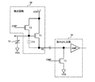
2.検出装置
図3に本実施形態の検出装置(赤外線検出装置)の第1の構成例を示す。第1の構成例は、上述した焦電流検出方式による赤外線の検出装置であって、焦電素子10と、焦電素子10の一端のノードである検出ノードN1の電圧を検出する検出回路20と、検出回路20の読み出しノードN2に接続される読み出し回路30とを含む。なお、本実施形態の検出装置は図3の構成に限定されず、その構成要素の一部を省略したり、他の構成要素に置き換えたり、他の構成要素を追加するなどの種々の変形実施が可能である。例えば、トランジスターT1〜T3としてN型トランジスターではなく、P型トランジスターを用いてもよい。
2. Detection Device FIG. 3 shows a first configuration example of the detection device (infrared detection device) of this embodiment. The first configuration example is an infrared detection device using the pyroelectric detection method described above, and includes a
焦電素子10(熱センサー素子、赤外線検出素子、熱型光検出素子、強誘電体素子)は、焦電体(焦電膜)と、焦電体を挟むように両端に設けられる第1、第2の電極とにより構成される。焦電体は、例えばPZT(チタン酸ジルコン酸鉛)などの強誘電体の膜により形成され、自発分極が発生している。この自発分極は、温度が高くなると小さくなるため、上述したように焦電素子の温度変化に伴って焦電流が生ずる。 The pyroelectric element 10 (thermal sensor element, infrared detection element, thermal detection element, ferroelectric element) includes a pyroelectric body (pyroelectric film) and first and second electrodes provided at both ends so as to sandwich the pyroelectric body. And a second electrode. The pyroelectric material is formed of a ferroelectric film such as PZT (lead zirconate titanate), and spontaneous polarization is generated. Since this spontaneous polarization becomes smaller as the temperature becomes higher, a pyroelectric current is generated as the pyroelectric element changes in temperature as described above.
検出回路20は、検出ノードN1によりゲートが制御される駆動トランジスターT1と、駆動トランジスターT1のドレインと検出ノードN1との間に設けられるプログラミング用トランジスターT2を含む。プログラミング用トランジスターT2は、制御信号CMPによりゲートが制御され、プログラム期間TPにおいてオン状態であり、読み出し期間TRにおいてオフ状態である。
The
読み出しノードN2は、駆動トランジスターT1のソースノードである。読み出し回路30は、駆動トランジスターT1のソースノードの電圧を読み出す。
The read node N2 is a source node of the drive transistor T1. The
読み出し回路30は、読み出しノードN2と低電位側電源ノードVSS(広義には第1の電源ノード)との間に設けられる電流パス用トランジスターT3を含む。電流パス用トランジスターT3は、プログラム期間TPにおいてオン状態であり、読み出し期間TRにおいてオフ状態である。
The
第1の構成例の動作について以下に説明する。プログラム期間TPにおいて、検出ノードN1が駆動トランジスターT1のしきい値電圧に対応する電圧値にプログラミングされる。また、プログラム期間TPに続く読み出し期間TRにおいて、読み出し回路30が検出回路20の検出結果の読み出し動作を行う。
The operation of the first configuration example will be described below. In the program period TP, the detection node N1 is programmed to a voltage value corresponding to the threshold voltage of the driving transistor T1. Further, in the reading period TR following the program period TP, the
具体的には、プログラム期間TPでは、制御信号CMPはHレベル(高電位レベル)であり、プログラミング用トランジスターT2及び電流パス用トランジスターT3はオン状態である。T2がオンすることで、検出ノードN1すなわち駆動トランジスターT1のゲートの電位が上昇する。T1のゲートの電位が上昇することで、T1がオン状態になりT1及びT3にドレイン電流が流れる。その結果、T1のゲートとソースとの間の寄生容量CSに印加される電圧が、T1のしきい値電圧に対応する値になり、その電圧値が寄生容量CSに充電される電荷により保持される。すなわちT1のしきい値電圧に対応する電圧値がプログラミングされる。なお、寄生容量CSの他に電圧保持用キャパシターをT1のゲートとソースとの間に設けてもよい。このプログラム期間TPでは、図示していない入射光制御機構(入射光制御部材、チョッパー)により赤外線は遮断されており、焦電素子10の温度は変化しない。なお、以下では入射光制御機構の一例としてチョッパーの例で説明する。
Specifically, in the program period TP, the control signal CMP is at the H level (high potential level), and the programming transistor T2 and the current path transistor T3 are in the on state. When T2 is turned on, the potential of the detection node N1, that is, the gate of the driving transistor T1, rises. As the potential of the gate of T1 rises, T1 is turned on and a drain current flows through T1 and T3. As a result, the voltage applied to the parasitic capacitance CS between the gate and source of T1 becomes a value corresponding to the threshold voltage of T1, and the voltage value is held by the charge charged in the parasitic capacitance CS. The That is, a voltage value corresponding to the threshold voltage of T1 is programmed. In addition to the parasitic capacitance CS, a voltage holding capacitor may be provided between the gate and the source of T1. In the program period TP, infrared rays are blocked by an incident light control mechanism (incident light control member, chopper) (not shown), and the temperature of the
一方、読み出し期間TRでは、制御信号CMPはLレベル(低電位レベル)であり、プログラミング用トランジスターT2及び電流パス用トランジスターT3はオフ状態である。また、読み出し期間TRでは、焦電素子10に赤外線が照射され、その結果焦電素子10の温度が上昇して焦電流が生ずる。この焦電流によりT1のゲート・ソース間寄生容量CSが充電されて、検出ノードN1の電位がプログラミングされた電圧(T1のしきい値電圧に対応する電圧値)からさらに上昇する。検出ノードN1の電位がT1のしきい値電圧より高くなることで、T1のドレイン電流が生じ、その結果読み出しノードN2の電位が上昇する。この電圧変化を読み出し回路30に含まれる増幅器(アンプ)AMPで増幅する。
On the other hand, in the read period TR, the control signal CMP is at the L level (low potential level), and the programming transistor T2 and the current path transistor T3 are in the off state. In the readout period TR, the
以上説明したように、プログラム期間TPにおいて検出ノードN1の電位が駆動トランジスターT1のしきい値電圧に対応する電圧値に設定されるから、T1のしきい値電圧のばらつきがあっても、ばらつきの影響を打ち消すことができる。複数のセンサーセルをアレイ状に配置したセンサーアレイなどでは、各センサーセルの検出回路に含まれるトランジスターのしきい値電圧のばらつきによって、赤外線源の温度が同じであっても読み出される出力信号電圧にばらつきが生じるおそれがある。本実施形態の検出装置によれば、検出回路に含まれるトランジスターのしきい値電圧のばらつきによる出力信号電圧のばらつきを低減することができる。その結果、検出装置の検出精度を高めることが可能になる。 As described above, the potential of the detection node N1 is set to a voltage value corresponding to the threshold voltage of the driving transistor T1 in the program period TP. The influence can be countered. In a sensor array in which a plurality of sensor cells are arranged in an array, the output signal voltage is read out even if the temperature of the infrared source is the same due to variations in the threshold voltage of the transistors included in the detection circuit of each sensor cell. Variation may occur. According to the detection device of this embodiment, it is possible to reduce variations in output signal voltage due to variations in threshold voltages of transistors included in the detection circuit. As a result, the detection accuracy of the detection device can be increased.
図4は、第1の構成例(図3)の信号波形の一例である。図4では、制御信号CMP、チョッパー信号CHP(広義には入射光制御信号)、駆動トランジスターT1のゲート・ソース間電圧VGS及び読み出しノードN2の電圧V(N2)(出力信号電圧)を示す。チョッパー信号CHPはチョッパー(広義には入射光制御機構)を制御する信号であって、アクティブレベルの期間には赤外線が焦電素子10に入射し、非アクティブレベルの期間には赤外線が遮断される。
FIG. 4 is an example of a signal waveform of the first configuration example (FIG. 3). FIG. 4 shows a control signal CMP, a chopper signal CHP (incident light control signal in a broad sense), a gate-source voltage VGS of the drive transistor T1, and a voltage V (N2) (output signal voltage) of the read node N2. The chopper signal CHP is a signal for controlling a chopper (incident light control mechanism in a broad sense), and infrared rays are incident on the
図4に示すように、プログラム期間TPでは、赤外線が遮断された状態で、駆動トランジスターT1のゲート・ソース間電圧VGSが、T1のしきい値電圧VTHに設定される(プログラミングされる)(図4のA3)。 As shown in FIG. 4, in the program period TP, the gate-source voltage VGS of the drive transistor T1 is set (programmed) to the threshold voltage VTH of T1 in a state where the infrared ray is cut off (FIG. 4). 4 A3).
次に読み出し期間TRでは、赤外線が入射して焦電流が発生し、焦電素子10の温度変化に応じてVGSが変化する。例えば図4では、対象物(赤外線源)の温度が低い場合にはA1に示すようにVGSが変化する。また、対象物の温度が高い場合にはA2に示すようにVGSが変化する。このVGSの変化に応じて、読み出しノードN2の電圧V(N2)は、B1(低温の場合)又はB2(高温の場合)に示すように変化する。
Next, in the readout period TR, infrared rays are incident to generate pyroelectric current, and VGS changes according to the temperature change of the
図5に、本実施形態の検出装置の第2の構成例を示す。第2の構成例は、上述した第1の構成例(図3)にさらに2つのトランジスターT4、T5を付加したものである。こうすることで、プログラム期間TPにおいて焦電素子10に電圧が印加されないようにすることができる。
FIG. 5 shows a second configuration example of the detection apparatus of the present embodiment. In the second configuration example, two transistors T4 and T5 are further added to the above-described first configuration example (FIG. 3). By doing so, it is possible to prevent a voltage from being applied to the
第2の構成例では、検出回路20は、P型のスイッチ用トランジスターT4及びN型のリセット用トランジスターT5を含む。スイッチ用トランジスターT4は、駆動トランジスターT1のゲートと検出ノードN1との間に設けられる。リセット用トランジスターT5は、検出ノードN1と低電位側電源ノードVSS(広義には第1の電源ノード)との間に設けられる。
In the second configuration example, the
スイッチ用トランジスターT4は、プログラム期間TPにおいてオフ状態であり、読み出し期間TRにおいてオン状態である。リセット用トランジスターT5は、プログラム期間TPにおいてオン状態であり、読み出し期間TRにおいてオフ状態である。したがって、プログラム期間TPでは、検出ノードN1は低電位側電源ノードVSSと電気的に接続され、T1のゲートと電気的に非接続になるから、焦電素子10には電圧が印加されない。一方読み出し期間TRでは、N1がT1のゲートに電気的に接続されるから、焦電流によって寄生容量CSが充電されてT1のゲート・ソース間電圧が変化する。こうすることで、プログラム期間TPにおいて焦電素子10に電圧が印加されなくなるから、検出装置の精度を高めることが可能になる。なお、駆動トランジスターT1、プログラミング用トランジスターT2及び電流パス用トランジスターT3の動作は、第1の構成例(図3)と同じであるから、説明を省略する。
The switching transistor T4 is in an off state during the program period TP and is in an on state during the reading period TR. The reset transistor T5 is in an on state in the program period TP and is in an off state in the read period TR. Therefore, in the program period TP, the detection node N1 is electrically connected to the low-potential side power supply node VSS and is not electrically connected to the gate of T1, so that no voltage is applied to the
図6に、本実施形態の検出装置の第3の構成例を示す。第3の構成例は、分極量検出方式による検出装置である。第3の構成例では、検出回路20は、P型の駆動トランジスターT11、N型のプログラミング用トランジスターT21、抵抗素子R1を含む。抵抗素子R1は検出ノードN1と低電位側電源ノードVSSとの間に設けられる。読み出し回路30は、上述した第1、第2の構成例と同一である。
FIG. 6 shows a third configuration example of the detection apparatus of the present embodiment. The third configuration example is a detection device using a polarization amount detection method. In the third configuration example, the
図7に、第3の構成例(図6)の信号波形の一例を示す。以下に、図7に従って第3の構成例の動作を説明する。 FIG. 7 shows an example of a signal waveform of the third configuration example (FIG. 6). The operation of the third configuration example will be described below with reference to FIG.
初期状態では、制御信号CMPはLレベル(低電位レベル)であり、プログラミング用トランジスターT21、電流パス用トランジスターT3はオフ状態である。また検出ノードN1はLレベルであるから、駆動トランジスターT11はオン状態であり、読み出しノードN2はHレベル(高電位レベル)となっている。 In the initial state, the control signal CMP is at the L level (low potential level), and the programming transistor T21 and the current path transistor T3 are off. Since the detection node N1 is at the L level, the drive transistor T11 is in the on state, and the read node N2 is at the H level (high potential level).
次のプログラム期間TPでは、制御信号CMPがHレベルになり、プログラミング用トランジスターT21、電流パス用トランジスターT3がオン状態になる。T11からT3にドレイン電流が流れるから、読み出しノードN2の電位はT11とT3とのオン抵抗の比で決定される電圧になる。一方、オン状態となったT21を介してN2の電位がN1にフィードバックされるから、検出ノードN1の電位は上昇する。N1の電位が上昇して、T11のゲート・ソース間電圧VGSがT11のしきい値電圧VTH(VTH<0とする)より高くなると、T11はオフ状態になるから、N1の電位は降下する。そしてT11のVGSがVTHより低くなると、再びT11がオン状態になるからN1の電位が上昇する。このようにして、最終的にはN1の電位はVDD+VTHに設定される。すなわちT11のゲート・ソース間電圧VGSはVTHに設定される(図7のC3)。この電圧値がT11のゲート・ソース間寄生容量CSにより保持されることで、しきい値電圧VTHに対応する電圧値がプログラミングされる。また、検出ノードN1の電位が上昇することで、焦電素子10に電圧が印加される。
In the next program period TP, the control signal CMP becomes H level, and the programming transistor T21 and the current path transistor T3 are turned on. Since the drain current flows from T11 to T3, the potential of the read node N2 becomes a voltage determined by the ratio of the on-resistance of T11 and T3. On the other hand, since the potential of N2 is fed back to N1 through T21 that is turned on, the potential of the detection node N1 rises. When the potential of N1 rises and the gate-source voltage VGS of T11 becomes higher than the threshold voltage VTH of T11 (VTH <0), T11 is turned off, so the potential of N1 drops. When the VGS of T11 becomes lower than VTH, the potential of N1 rises because T11 is turned on again. In this way, the potential of N1 is finally set to VDD + VTH. That is, the gate-source voltage VGS of T11 is set to VTH (C3 in FIG. 7). The voltage value corresponding to the threshold voltage VTH is programmed by holding this voltage value by the gate-source parasitic capacitance CS of T11. Further, a voltage is applied to the
続く読み出し期間TRでは、制御信号CMPがLレベルになり、T21、T3はオフ状態になる。焦電素子10に電圧が印加されなくなるから、焦電素子10から抵抗素子R1を介して放電電流が流れる。この放電によって検出ノードN1の電位が降下することでT11がオン状態となり、読み出しノードN2の電位が上昇する。焦電素子10の温度によって分極量が異なるために、N1の電圧降下の速さが異なり、その結果N2の電圧上昇の速さが異なってくる。例えば図7では、低温の場合にはC1、D1に示すように急速に変化し、高温の場合にはC2、D2に示すように緩やかに変化する。この電圧変化を検出することで、赤外線源の温度を測定することが可能になる。
In the subsequent read period TR, the control signal CMP becomes L level, and T21 and T3 are turned off. Since no voltage is applied to the
図8に、本実施形態の検出装置の第3の構成例の変形例を示す。図8の構成では、読み出し回路30は、さらに出力リセット用トランジスターT4を含む。この出力リセット用トランジスターT4は、読み出しノードN2と低電位側電源ノードVSSとの間に設けられ、読み出し期間TRの直前(すなわちプログラム期間TPの最終期間)に読み出しノードN2の電位をLレベル(低電位レベル)にリセットする。こうすることで、読み出し期間TRにおける読み出しノードN2の電圧変化が大きくなるから、電圧変化の検出が容易になり、さらに温度測定の精度を高めることができる。
FIG. 8 shows a modification of the third configuration example of the detection apparatus of the present embodiment. In the configuration of FIG. 8, the
図9に、第3の構成例の変形例(図8)の信号波形の一例を示す。初期状態及びプログラム期間TPの前半における動作は、図7に示した第3の構成例の動作と同じである。プログラム期間TPの前半で、検出ノードN1の電位がVDD+VTH(VTHはT11のしきい値電圧でありVTH<0とする)に設定された後に、制御信号CMPがLレベルになり、リセット信号RSTが一時的にHレベルになる。リセット信号RSTがHレベルになることで出力リセット用トランジスターT4がオン状態になるから、読み出しノードN2の電位がLレベル(又はLレベル近く)まで降下する(図9のF3)。 FIG. 9 shows an example of a signal waveform of a modification (FIG. 8) of the third configuration example. The operation in the initial state and the first half of the program period TP is the same as the operation of the third configuration example shown in FIG. In the first half of the program period TP, after the potential of the detection node N1 is set to VDD + VTH (VTH is a threshold voltage of T11 and VTH <0), the control signal CMP becomes L level, and the reset signal RST is Temporarily becomes H level. Since the output reset transistor T4 is turned on when the reset signal RST becomes H level, the potential of the read node N2 drops to L level (or close to L level) (F3 in FIG. 9).
続く読み出し期間TRでは、上述したように、焦電素子10の放電によって検出ノードN1の電位が降下することでT11がオン状態となり、読み出しノードN2の電位が上昇する。例えば図9では、低温の場合にはE1、F1に示すように急速に変化し、高温の場合にはE2、F2に示すように緩やかに変化する。この電圧変化を検出することで、赤外線源の温度を測定することが可能になる。
In the subsequent readout period TR, as described above, the potential of the detection node N1 drops due to the discharge of the
図10に、本実施形態の検出装置の第4の構成例を示す。第4の構成例は、焦電流検出方式による検出装置であって、駆動トランジスターT1の電流供給能力のばらつきを補償する補償回路40を含む。補償回路40は、読み出しノードN2と低電位側電源ノードVSS(広義には第1の電源ノード)との間に設けられる抵抗素子R2を含む。抵抗素子R2を設けることで電流パスが形成されるから、読み出し回路30の電流パス用トランジスターT3を省略することができる。
In FIG. 10, the 4th structural example of the detection apparatus of this embodiment is shown. The fourth configuration example is a detection device using a pyroelectric current detection method, and includes a
既に説明したように、本実施形態の検出装置によれば、駆動トランジスターT1のしきい値電圧のばらつきを補償することができる。しかし駆動トランジスターT1の移動度のばらつきや温度のばらつき等に起因する電流供給能力のばらつきを補償することはできない。第4の構成例によれば、補償回路40を設けることで電流供給能力のばらつきを補償し、より精度の高い検出装置を実現することが可能になる。
As already described, according to the detection device of the present embodiment, it is possible to compensate for variations in the threshold voltage of the drive transistor T1. However, it is not possible to compensate for variations in current supply capability due to variations in mobility and temperature in the drive transistor T1. According to the fourth configuration example, by providing the
駆動トランジスターT1の電流供給能力が高い場合には、抵抗素子R2を流れる電流が増加する。そうすると読み出しノードN2の電位が上昇するから、T1のドレイン・ソース間電圧が低下する。T1のドレイン・ソース間電圧が低下することで、T1のドレイン電流が減少する。 When the current supply capability of the driving transistor T1 is high, the current flowing through the resistance element R2 increases. As a result, the potential of the read node N2 rises, so that the drain-source voltage of T1 falls. As the drain-source voltage of T1 decreases, the drain current of T1 decreases.
逆に駆動トランジスターT1の電流供給能力が低い場合には、抵抗素子R2を流れる電流が減少する。そうすると読み出しノードN2の電位が低下するから、T1のドレイン・ソース間電圧が上昇する。T1のドレイン・ソース間電圧が上昇することで、T1のドレイン電流が増加する。 Conversely, when the current supply capability of the driving transistor T1 is low, the current flowing through the resistance element R2 decreases. As a result, the potential of the read node N2 decreases, and the drain-source voltage of T1 increases. As the drain-source voltage of T1 increases, the drain current of T1 increases.
このように、補償回路40を設けることで、トランジスターの電流供給能力のばらつきの影響を打ち消す効果が得られるから、T1の電流供給能力のばらつきを抑えることができる。その結果、より精度の高い検出装置を実現することが可能になる。
Thus, by providing the
図11に、本実施形態の検出装置の第5の構成例を示す。第5の構成例は、焦電流検出方式による検出装置であって、第4の構成例と同様に補償回路40を含む。第5の構成例では、補償回路40は、2つのトランジスターT6、T7及び抵抗素子R3を含む。トランジスターT6は、読み出しノードN2と低電位側電源ノードVSS(広義には第1の電源ノード)との間に設けられる。抵抗素子R3は、高電位側電源ノードVDD(広義には第2の電源ノード)とT6のゲートとの間に設けられる。トランジスターT7は、T6のゲートと低電位側電源ノードVSSとの間に設けられ、T7のゲートには基準電圧VREFが印加される。第4の構成例と同様に、第5の構成例によれば、補償回路40を設けることでトランジスターの電流供給能力のばらつきを補償し、より精度の高い検出装置を実現することが可能になる。
FIG. 11 shows a fifth configuration example of the detection apparatus of the present embodiment. The fifth configuration example is a detection device based on a pyroelectric current detection method, and includes a
各トランジスターの電流供給能力は同じようにばらつくと考えられる。例えば、駆動トランジスターT1の電流供給能力が高い方にばらつく場合には、T7の電流供給能力も高くなる。T7の電流供給能力が高くなれば、T7のドレインの電位、即ちT6のゲートの電位が低下する。T6のゲート・ソース間電圧が低下することで、読み出しノードN2の電位が上昇し、T1のドレイン・ソース間電圧が低下する。T1のドレイン・ソース間電圧が低下することで、T1のドレイン電流が減少する。 The current supply capability of each transistor is considered to vary in the same way. For example, when the current supply capability of the drive transistor T1 varies in the higher one, the current supply capability of T7 is also increased. When the current supply capability of T7 increases, the potential of the drain of T7, that is, the potential of the gate of T6 decreases. As the gate-source voltage at T6 decreases, the potential of the read node N2 increases, and the drain-source voltage at T1 decreases. As the drain-source voltage of T1 decreases, the drain current of T1 decreases.
逆に、トランジスターの電流供給能力が低い方にばらつく場合には、T6のゲート・ソース間電圧が上昇して、読み出しノードN2の電位が低下する。その結果、T1のドレイン・ソース間電圧が上昇して、T1のドレイン電流が増加する。 On the contrary, when the current supply capability of the transistor varies toward the lower side, the gate-source voltage of T6 increases and the potential of the read node N2 decreases. As a result, the drain-source voltage of T1 increases and the drain current of T1 increases.
このように、補償回路40を設けることで、トランジスターの電流供給能力のばらつきの影響を打ち消す効果が得られるから、T1の電流供給能力のばらつきを抑えることができる。その結果、より精度の高い検出装置を実現することが可能になる。
Thus, by providing the
以上説明したように、本実施形態の検出装置によれば、トランジスターのしきい値電圧のばらつきを補償することができるから、高精度の赤外線検出等が可能になる。さらに補償回路を設けることで、トランジスターの移動度や温度等のばらつきに起因する電流供給能力のばらつきを補償することができるから、検出精度をさらに向上させることが可能になる。 As described above, according to the detection device of the present embodiment, variations in the threshold voltage of the transistor can be compensated, and therefore, highly accurate infrared detection and the like can be performed. Furthermore, by providing a compensation circuit, it is possible to compensate for variations in current supply capability due to variations in transistor mobility, temperature, and the like, so that detection accuracy can be further improved.
なお、後述するセンサーアレイの構成において、図10、図11のように補償回路40を各センサーセルごとに設ける構成としてもよいし、また各列(カラム)毎に設ける構成としてもよい。
In the configuration of the sensor array to be described later, the
3.センサーデバイス
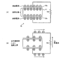
図12(A)に本実施形態のセンサーデバイスの構成例を示す。このセンサーデバイスは、センサーアレイ100と、行選択回路(行ドライバー)110と、読み出し回路120とを含む。またA/D変換部130、カラム走査回路140、制御回路150を含むことができる。このセンサーデバイスを用いることで、例えばナイトビジョン機器などに用いられる赤外線カメラなどを実現できる。
3. Sensor Device FIG. 12A shows a configuration example of the sensor device of the present embodiment. The sensor device includes a
センサーアレイ100(焦点面アレイ)には、複数のセンサーセルが配列(配置)される。また複数の行線(ワード線、走査線)と複数の列線(データ線)が設けられる。なお行線及び列線の一方の本数が1本であってもよい。例えば行線が1本である場合には、図12(A)において行線に沿った方向(横方向)に複数のセンサーセルが配列される。一方、列線が1本である場合には、列線に沿った方向(縦方向)に複数のセンサーセルが配列される。 A plurality of sensor cells are arranged (arranged) in the sensor array 100 (focal plane array). A plurality of row lines (word lines, scanning lines) and a plurality of column lines (data lines) are provided. One of the row lines and the column lines may be one. For example, when there is one row line, a plurality of sensor cells are arranged in a direction (lateral direction) along the row line in FIG. On the other hand, when there is one column line, a plurality of sensor cells are arranged in a direction (vertical direction) along the column line.
図12(B)に示すように、センサーアレイ100の各センサーセルは、各行線と各列線の交差位置に対応する場所に配置(形成)される。例えば図12(B)のセンサーセルは、行線WL1と列線DL1の交差位置に対応する場所に配置されている。他のセンサーセルも同様である。
As shown in FIG. 12B, each sensor cell of the
行選択回路110は、1又は複数の行線に接続される。そして各行線の選択動作を行う。例えば図12(B)のようなQVGA(320×240画素)のセンサーアレイ100(焦点面アレイ)を例にとれば、行線WL0、WL1、WL2・・・・WL239を順次選択(走査)する動作を行う。即ちこれらの行線を選択する信号(ワード選択信号)をセンサーアレイ100に出力する。
The
読み出し回路120は、1又は複数の列線に接続される。そして各列線の読み出し動作を行う。QVGAのセンサーアレイ100を例にとれば、列線DL0、DL1、DL2・・・・DL319からの検出信号(検出電流、検出電荷)を読み出す動作を行う。この読み出し回路120は、例えば既に説明した検出装置の第1〜第5の構成例の読み出し回路30を、各列線に対応させて配置することで実現できる。
The
A/D変換部130は、読み出し回路120において取得された検出電圧(測定電圧、到達電圧)をデジタルデータにA/D変換する処理を行う。そしてA/D変換後のデジタルデータDOUTを出力する。具体的には、A/D変換部130には、複数の列線の各列線に対応して各A/D変換器が設けられる。そして、各A/D変換器は、対応する列線において読み出し回路120により取得された検出電圧のA/D変換処理を行う。なお、複数の列線に対応して1つのA/D変換器を設け、この1つのA/D変換器を用いて、複数の列線の検出電圧を時分割にA/D変換してもよい。
The A /
カラム走査回路140は、各カラム(列)を順次選択(走査)して、各カラムのA/D変換後のデジタルデータを時系列データとして出力するための動作を行う。なお、カラム走査回路140を設けずに、各カラムのデジタルデータを並行して(パラレルに)出力してもよい。
The
制御回路150(タイミング生成回路)は、各種の制御信号を生成して、行選択回路110、読み出し回路120、A/D変換部130、カラム走査回路140に出力する。例えば充電や放電(リセット)の制御信号を生成して出力する。或いは、各回路のタイミングを制御する信号を生成して出力する。
The control circuit 150 (timing generation circuit) generates various control signals and outputs them to the
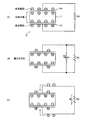
図13に、センサーアレイ100や読み出し回路120の詳細な構成例を示す。なお、図13では、センサーセル及び読み出し回路として第1の構成例(図3)を用いているが、図5、図6、図8、図10、図11に示した各種構成・手法を組み合わせた変形実施も可能である。
FIG. 13 shows a detailed configuration example of the
各センサーセルは、焦電素子10(広義には熱センサー素子)と、焦電素子10の一端のノードである検出ノードN1の電圧を検出する検出回路20とを含む。検出回路20は、検出ノードN1によりゲートが制御される駆動トランジスターT1を含む。プログラム期間TPにおいて、検出ノードN1が駆動トランジスターT1のしきい値電圧に対応する電圧値にプログラミングされる。プログラム期間TPに続く読み出し期間TRにおいて、読み出し回路120が、1又は複数の列線DL(DL0〜DL319)の各列線に接続される検出回路の検出結果の読み出し動作を行う。
Each sensor cell includes a pyroelectric element 10 (thermal sensor element in a broad sense) and a
具体的には、例えば行線WL0が選択される場合には、行線WL0にゲートが接続されるトランジスターTWがオン状態になる。そして行線WL0に対応する1又は複数のセンサーセルが、それぞれ対応する列線DL(DL0〜DL319)に電気的に接続される。この時、行線WL0以外の行線WL(WL1〜WL239)は非選択である。 Specifically, for example, when the row line WL0 is selected, the transistor TW whose gate is connected to the row line WL0 is turned on. Then, one or a plurality of sensor cells corresponding to the row line WL0 are electrically connected to the corresponding column lines DL (DL0 to DL319). At this time, the row lines WL (WL1 to WL239) other than the row line WL0 are not selected.
プログラム期間TPでは、制御信号CMPはHレベル(高電位レベル)であり、選択されたセンサーセルのプログラミング用トランジスターT2及び読み出し回路120の電流パス用トランジスターT3はオン状態である。T2がオンすることで、検出ノードN1すなわち駆動トランジスターT1のゲートの電位が上昇する。T1のゲートの電位が上昇することで、T1がオン状態になりT1及びT3にドレイン電流が流れる。その結果、T1のゲートとソースとの間の寄生容量CSに印加される電圧が、T1のしきい値電圧に対応する値になり、その電圧値が寄生容量CSに充電される電荷により保持される。すなわちT1のしきい値電圧に対応する電圧値がプログラミングされる。なお、寄生容量CSの他に電圧保持用キャパシターをT1のゲートとソースとの間に設けてもよい。このプログラム期間TPでは、チョッパーにより赤外線は遮断されており、焦電素子10の温度は変化しない。
In the program period TP, the control signal CMP is at the H level (high potential level), and the programming transistor T2 of the selected sensor cell and the current path transistor T3 of the
一方、読み出し期間TRでは、制御信号CMPはLレベル(低電位レベル)であり、プログラミング用トランジスターT2及び電流パス用トランジスターT3はオフ状態である。また、読み出し期間TRでは、焦電素子10に赤外線が照射され、その結果焦電素子10の温度が上昇して焦電流が生ずる。この焦電流によりT1のゲート・ソース間寄生容量CSが充電されて、検出ノードN1の電位が上昇する。検出ノードN1の電位の変化に応じて、読み出しノードN2の電位が変化するから、この変化を読み出し回路120に含まれる増幅器(アンプ)AMPで増幅する。
On the other hand, in the read period TR, the control signal CMP is at the L level (low potential level), and the programming transistor T2 and the current path transistor T3 are in the off state. In the readout period TR, the
このようにして、行線WL0に対応する1又は複数のセンサーセルからの検出信号が列(カラム)毎に読み出される。その後、他の行線WL(WL1〜WL239)が順次選択され、上記と同様にして各センサーセルから検出信号が読み出される。 In this way, detection signals from one or more sensor cells corresponding to the row line WL0 are read out for each column. Thereafter, the other row lines WL (WL1 to WL239) are sequentially selected, and the detection signal is read from each sensor cell in the same manner as described above.
以上説明したように、初期状態(すなわち赤外線が遮断されている状態)での検出ノードN1の電位が駆動トランジスターT1のしきい値電圧に対応する電圧値に設定されるから、T1のしきい値電圧のばらつきがある場合でも、ばらつきの影響を抑えることができる。 As described above, since the potential of the detection node N1 in the initial state (that is, the state where infrared rays are blocked) is set to a voltage value corresponding to the threshold voltage of the driving transistor T1, the threshold value of T1 is set. Even when there is a variation in voltage, the influence of the variation can be suppressed.
センサーアレイなどでは、各センサーセルのトランジスターのしきい値電圧のばらつきによって、赤外線源の温度が同じであっても、センサーセル間で読み出される信号電圧にばらつきが生じるおそれがある。本実施形態のセンサーデバイスによれば、各センサーセルに含まれるトランジスターのしきい値電圧のばらつきによる検出信号電圧(読み出し信号電圧)のばらつきを低減することができる。その結果、センサーデバイスの検出精度(分解能)を高めることが可能になる。 In a sensor array or the like, due to variations in the threshold voltage of the transistors in each sensor cell, there may be variations in the signal voltage read between the sensor cells even if the temperature of the infrared source is the same. According to the sensor device of this embodiment, it is possible to reduce variations in detection signal voltage (readout signal voltage) due to variations in threshold voltage of transistors included in each sensor cell. As a result, the detection accuracy (resolution) of the sensor device can be increased.
なお、プログラム期間TP及び読み出し期間TRのタイミングについては、上記のように順次1行毎にプログラミングと読み出しとを繰り返していく方法の他に、種々の方法が可能である。例えば、赤外線計測に先立って全てのセンサーセルについて同時にプログラミングを行う方法も可能である。 As for the timing of the program period TP and the read period TR, various methods are possible in addition to the method of sequentially repeating the programming and reading for each row as described above. For example, a method of simultaneously programming all sensor cells prior to infrared measurement is also possible.
4.電子機器
図14に本実施形態の検出装置やセンサーデバイスを含む電子機器の構成例を示す。この電子機器は、例えば赤外線カメラであって、光学系200、センサーデバイス210、画像処理部220、処理部230、記憶部240、操作部250、表示部260を含む。なお本実施形態の電子機器は図14の構成に限定されず、その構成要素の一部(例えば光学系、操作部、表示部等)を省略したり、他の構成要素を追加するなどの種々の変形実施が可能である。
4). Electronic Device FIG. 14 shows a configuration example of an electronic device including the detection apparatus and sensor device of the present embodiment. The electronic apparatus is, for example, an infrared camera, and includes an
光学系200は、例えば1又は複数のレンズや、これらのレンズを駆動する駆動部などを含む。そしてセンサーデバイス210への物体像の結像などを行う。また必要であればフォーカス調整なども行う。
The
センサーデバイス210は、図12(A)等で説明したものであり、物体像の撮像処理を行う。画像処理部220は、センサーデバイス210からのデジタルの画像データ(画素データ)に基づいて、画像補正処理などの各種の画像処理を行う。
The
処理部230は、電子機器の全体の制御を行ったり、電子機器内の各ブロックの制御を行う。この処理部230は、例えばCPU等により実現される。記憶部240は、各種の情報を記憶するものであり、例えば処理部230や画像処理部220のワーク領域として機能する。操作部250は、ユーザが電子機器を操作するためのインターフェースとなるものであり、例えば各種ボタンやGUI(Graphical User Interface)画面などにより実現される。表示部260は、例えばセンサーデバイス210により取得された画像やGUI画面などを表示するものであり、液晶ディスプレイや有機ELディスプレイなどの各種のディスプレイや投射型表示装置などにより実現される。
The
なお本実施形態は、FPA(Focal Plane Array:焦点面アレイ)を用いた赤外線カメラや赤外線カメラを用いた電子機器に適用できる。赤外線カメラを適用した電子機器としては、例えば夜間の物体像を撮像するナイトビジョン機器、物体の温度分布を取得するサーモグラフィー機器、人の侵入を検知する侵入検知機器、物体の物理情報の解析(測定)を行う解析機器(測定機器)、火や発熱を検知するセキュリティー機器、工場などに設けられるFA(Factory Automation)機器などが想定できる。ナイトビジョン機器を車載機器に適用すれば、車の走行時に夜間の人等の姿を検知して表示することができる。またサーモグラフィー機器に適用すれば、インフルエンザ検疫等に利用することができる。 The present embodiment can be applied to an infrared camera using an FPA (Focal Plane Array) and an electronic device using the infrared camera. Electronic devices to which infrared cameras are applied include, for example, night vision devices that capture night-time object images, thermographic devices that acquire the temperature distribution of objects, intrusion detection devices that detect human intrusions, and analysis (measurement of physical information on objects) Analysis equipment (measuring equipment), security equipment that detects fire and heat generation, FA (Factory Automation) equipment installed in factories, etc. can be assumed. If a night vision device is applied to an in-vehicle device, it is possible to detect and display the appearance of a person at night when the vehicle is running. If applied to a thermographic device, it can be used for influenza quarantine.
なお、以上のように本実施形態について詳細に説明したが、本発明の新規事項および効果から実体的に逸脱しない多くの変形が可能であることは当業者には容易に理解できるであろう。従って、このような変形例はすべて本発明の範囲に含まれるものとする。例えば、明細書又は図面において、少なくとも一度、より広義または同義な異なる用語(第1の電源ノード、第2の電源ノード)と共に記載された用語(VSSノード、VDDノード)は、明細書又は図面のいかなる箇所においても、その異なる用語に置き換えることができる。また検出装置、センサーデバイス及び電子機器の構成、動作も本実施形態で説明したものに限定されず、種々の変形実施が可能である。 Although the present embodiment has been described in detail as described above, it will be easily understood by those skilled in the art that many modifications can be made without departing from the novel matters and effects of the present invention. Accordingly, all such modifications are intended to be included in the scope of the present invention. For example, in the specification or the drawings, terms (VSS node, VDD node) described together with different terms (first power supply node, second power supply node) having a broader meaning or the same meaning at least once are described in the specification or the drawings. It can be replaced by the different terms at any point. Further, the configurations and operations of the detection device, the sensor device, and the electronic apparatus are not limited to those described in this embodiment, and various modifications can be made.
10 焦電素子、11 焦電体、12 電極、20 検出回路、
30 読み出し回路、40 補償回路、100 センサーアレイ、
110 行選択回路(行ドライバー)、120 読み出し回路、130 A/D変換部、
140 カラム走査回路、150 制御回路、200 光学系、
210 センサーデバイス、220 画像処理部、230 処理部(CPU)、
240 記憶部、250 操作部、260 表示部、
CMP 制御信号、CS ゲート・ソース間寄生容量、N1 検出ノード、
N2 読み出しノード、T1 駆動トランジスター、
T2 プログラミング用トランジスター、T3 電流パス用トランジスター
10 pyroelectric elements, 11 pyroelectric bodies, 12 electrodes, 20 detection circuit,
30 readout circuit, 40 compensation circuit, 100 sensor array,
110 row selection circuit (row driver), 120 readout circuit, 130 A / D converter,
140 column scanning circuit, 150 control circuit, 200 optical system,
210 sensor device, 220 image processing unit, 230 processing unit (CPU),
240 storage unit, 250 operation unit, 260 display unit,
CMP control signal, CS gate-source parasitic capacitance, N1 detection node,
N2 readout node, T1 drive transistor,
T2 programming transistor, T3 current path transistor
Claims (9)
前記熱センサー素子の一端のノードである検出ノードの電圧を検出する検出回路と、
前記検出回路の読み出しノードに接続される読み出し回路とを含み、
前記検出回路は、
前記検出ノードによりゲートが制御される駆動トランジスターと、
前記駆動トランジスターのゲートノードと前記検出ノードとの間に設けられるスイッチ用トランジスターと、
前記検出ノードと第1の電源ノードとの間に設けられるリセット用トランジスターとを含み、
プログラム期間において、前記駆動トランジスターの前記ゲートノードが前記駆動トランジスターのしきい値電圧に対応する電圧値に設定され、
前記プログラム期間の後の読み出し期間において、前記読み出し回路が前記検出回路の検出結果の読み出し動作を行い、
前記スイッチ用トランジスターは、前記プログラム期間においてオフ状態であり、前記読み出し期間においてオン状態であり、
前記リセット用トランジスターは、前記プログラム期間においてオン状態であり、前記読み出し期間においてオフ状態であることを特徴とする検出装置。 A thermal sensor element;
A detection circuit for detecting a voltage of a detection node which is a node at one end of the thermal sensor element;
A readout circuit connected to a readout node of the detection circuit,
The detection circuit includes:
A driving transistor whose gate is controlled by the detection node ;
A switching transistor provided between a gate node of the driving transistor and the detection node;
A resetting transistor provided between the detection node and the first power supply node,
In the program period, the gate node of the driving transistor is set to a voltage value corresponding to the threshold voltage of the driving transistor,
In the read period after the program period, the read circuit have line reading operation of the detection result of the detecting circuit,
The switching transistor is in an off state in the program period, and is in an on state in the read period,
The detection device , wherein the reset transistor is in an on state in the program period and is in an off state in the read period .
前記検出回路は、
前記駆動トランジスターのドレインノードと前記ゲートノードとの間に設けられるプログラミング用トランジスターを含み、
前記プログラミング用トランジスターは、前記プログラム期間においてオン状態であり、前記読み出し期間においてオフ状態であることを特徴とする検出装置。 In claim 1,
The detection circuit includes:
A programming transistor provided between a drain node of the driving transistor and the gate node;
The detection device according to claim 1, wherein the programming transistor is in an on state during the programming period and is in an off state during the reading period.
前記読み出しノードは、前記駆動トランジスターのソースノードであり、
前記読み出し回路は、前記駆動トランジスターの前記ソースノードの電圧を読み出すことを特徴とする検出装置。 In claim 1 or 2,
The read node is a source node of the drive transistor;
The detection device, wherein the reading circuit reads a voltage of the source node of the driving transistor.
前記読み出しノードと前記第1の電源ノードとの間に設けられ、前記駆動トランジスターの電流供給能力のばらつきを補償する補償回路を含むことを特徴とする検出装置。 In any one of Claims 1 thru | or 3,
Wherein provided between the read node and the first power supply node, detecting device characterized by comprising a compensation circuit for compensating a variation in current supply capability of the drive transistor.
前記補償回路は、前記読み出しノードと前記第1の電源ノードとの間に設けられる抵抗素子又はトランジスターを含むことを特徴とする検出装置。 In claim 4,
The detection device includes a resistance element or a transistor provided between the readout node and the first power supply node.
前記読み出し回路は、前記読み出しノードと前記第1の電源ノードとの間に設けられる電流パス用トランジスターを含み、
前記電流パス用トランジスターは、前記プログラム期間においてオン状態であり、前記読み出し期間においてオフ状態であることを特徴とする検出装置。 In any one of Claims 1 thru | or 5 ,
The read circuit includes a current path transistor provided between the read node and the first power supply node,
The detection device, wherein the current path transistor is in an on state during the program period and is in an off state during the read period.
1又は複数の行線と、
1又は複数の列線と、
前記1又は複数の行線に接続される行選択回路と、
前記1又は複数の列線に接続される読み出し回路とを含み、
前記複数のセンサーセルの各センサーセルは、熱センサー素子と、前記熱センサー素子の一端のノードである検出ノードの電圧を検出する検出回路とを含み、
前記検出回路は、
前記検出ノードによりゲートが制御される駆動トランジスターと、
前記駆動トランジスターのゲートノードと前記検出ノードとの間に設けられるスイッチ用トランジスターと、
前記検出ノードと第1の電源ノードとの間に設けられるリセット用トランジスターとを含み、
プログラム期間において、前記駆動トランジスターの前記ゲートノードが前記駆動トランジスターのしきい値電圧に対応する電圧値に設定され、
前記プログラム期間の後の読み出し期間において、前記読み出し回路が、前記1又は複数の列線の各列線に接続される前記検出回路の検出結果の読み出し動作を行い、
前記スイッチ用トランジスターは、前記プログラム期間においてオフ状態であり、前記読み出し期間においてオン状態であり、
前記リセット用トランジスターは、前記プログラム期間においてオン状態であり、前記読み出し期間においてオフ状態であることを特徴とするセンサーデバイス。 A sensor array having a plurality of sensor cells;
One or more row lines;
One or more column lines;
A row selection circuit connected to the one or more row lines;
A readout circuit connected to the one or more column lines,
Each sensor cell of the plurality of sensor cells includes a thermal sensor element and a detection circuit that detects a voltage of a detection node that is a node at one end of the thermal sensor element,
The detection circuit includes:
A driving transistor whose gate is controlled by the detection node ;
A switching transistor provided between a gate node of the driving transistor and the detection node;
A resetting transistor provided between the detection node and the first power supply node,
In the program period, the gate node of the driving transistor is set to a voltage value corresponding to the threshold voltage of the driving transistor,
In the read period after the program period, the read circuit, have rows detection result of the read operation of the detection circuit connected to each column line of the one or more column lines,
The switching transistor is in an off state in the program period, and is in an on state in the read period,
The sensor device according to claim 1, wherein the reset transistor is in an on state during the program period and is in an off state during the readout period .
Priority Applications (4)
| Application Number | Priority Date | Filing Date | Title |
|---|---|---|---|
| JP2010260001A JP5578045B2 (en) | 2010-01-26 | 2010-11-22 | Detection apparatus, sensor device, and electronic apparatus |
| CN2011100258005A CN102192789A (en) | 2010-01-26 | 2011-01-24 | Detection device, sensor device, and electronic device |
| EP11151983.1A EP2357457A3 (en) | 2010-01-26 | 2011-01-25 | Detection device, sensor device, and electronic device |
| US13/013,011 US9222838B2 (en) | 2010-01-26 | 2011-01-25 | Detection device, sensor device, and electronic device |
Applications Claiming Priority (3)
| Application Number | Priority Date | Filing Date | Title |
|---|---|---|---|
| JP2010014135 | 2010-01-26 | ||
| JP2010014135 | 2010-01-26 | ||
| JP2010260001A JP5578045B2 (en) | 2010-01-26 | 2010-11-22 | Detection apparatus, sensor device, and electronic apparatus |
Publications (3)
| Publication Number | Publication Date |
|---|---|
| JP2011174918A JP2011174918A (en) | 2011-09-08 |
| JP2011174918A5 JP2011174918A5 (en) | 2013-12-05 |
| JP5578045B2 true JP5578045B2 (en) | 2014-08-27 |
Family
ID=43902701
Family Applications (1)
| Application Number | Title | Priority Date | Filing Date |
|---|---|---|---|
| JP2010260001A Expired - Fee Related JP5578045B2 (en) | 2010-01-26 | 2010-11-22 | Detection apparatus, sensor device, and electronic apparatus |
Country Status (4)
| Country | Link |
|---|---|
| US (1) | US9222838B2 (en) |
| EP (1) | EP2357457A3 (en) |
| JP (1) | JP5578045B2 (en) |
| CN (1) | CN102192789A (en) |
Families Citing this family (6)
| Publication number | Priority date | Publication date | Assignee | Title |
|---|---|---|---|---|
| JP2014153308A (en) * | 2013-02-13 | 2014-08-25 | Azbil Corp | Human detecting device and human detecting method |
| JP6202245B2 (en) * | 2013-03-22 | 2017-09-27 | セイコーエプソン株式会社 | Infrared sensor and thermoelectric conversion element |
| US10446116B2 (en) | 2016-09-23 | 2019-10-15 | Apple Inc. | Temperature sensor on display active area |
| CN107657923B (en) | 2017-11-15 | 2020-02-21 | 合肥鑫晟光电科技有限公司 | Detection method of pixel circuit, driving method of display panel, display device and pixel circuit |
| US11594034B1 (en) * | 2020-08-21 | 2023-02-28 | Vivint, Inc. | Techniques for a smart monitoring system |
| US11244547B1 (en) | 2020-08-21 | 2022-02-08 | Vivint, Inc. | Smart monitoring system |
Family Cites Families (24)
| Publication number | Priority date | Publication date | Assignee | Title |
|---|---|---|---|---|
| JPS59142427A (en) * | 1983-02-02 | 1984-08-15 | Matsushita Electric Ind Co Ltd | Heat sensor |
| US4897547A (en) * | 1986-09-26 | 1990-01-30 | Honeywell Inc. | Gate coupled input circuit |
| JPH01102321A (en) * | 1987-10-16 | 1989-04-20 | Hamamatsu Photonics Kk | Detecting device of infrared ray and manufacture thereof |
| US5043820A (en) * | 1989-03-27 | 1991-08-27 | Hughes Aircraft Company | Focal plane array readout employing one capacitive feedback transimpedance amplifier for each column |
| US5144133A (en) * | 1991-04-04 | 1992-09-01 | Texas Instruments Incorporated | Uncooled infrared detector readout monolithic integrated circuit with individual pixel signal processing |
| JPH06265411A (en) * | 1993-03-16 | 1994-09-22 | Fujitsu Ltd | Infrared image picking up method and its device |
| US5926217A (en) * | 1993-07-27 | 1999-07-20 | Drs Technologies, Inc. | Focal plane array integrated circuit with individual pixel signal processing |
| JP3635681B2 (en) * | 1994-07-15 | 2005-04-06 | ソニー株式会社 | Bias circuit adjustment method, charge transfer device, charge detection device, and adjustment method thereof |
| US5869857A (en) | 1997-04-07 | 1999-02-09 | Chen; Pao-Jung | CMOS photodetectors with wide range operating region |
| DE69943177D1 (en) * | 1998-02-27 | 2011-03-24 | Panasonic Elec Works Co Ltd | Infrared radiation detector |
| JP3536896B2 (en) * | 1998-03-24 | 2004-06-14 | 富士ゼロックス株式会社 | Solid-state imaging device |
| JP3031332B2 (en) * | 1998-05-06 | 2000-04-10 | 日本電気株式会社 | Image sensor |
| JP3793033B2 (en) * | 2001-03-29 | 2006-07-05 | 株式会社東芝 | Infrared sensor and driving method thereof |
| SG111050A1 (en) * | 2001-09-10 | 2005-05-30 | Matsushita Electric Works Ltd | Object detecting device with a pyroelectric sensor |
| JP2003101005A (en) * | 2001-09-27 | 2003-04-04 | Citizen Watch Co Ltd | Solid-state image pickup device |
| JP4075880B2 (en) * | 2004-09-29 | 2008-04-16 | セイコーエプソン株式会社 | Electro-optical device, data line driving circuit, signal processing circuit, and electronic device |
| JP4331160B2 (en) * | 2005-12-07 | 2009-09-16 | 株式会社東芝 | Infrared sensor and driving method thereof |
| JP2007181106A (en) * | 2005-12-28 | 2007-07-12 | Matsushita Electric Ind Co Ltd | Sensor and method of driving the same |
| US7969494B2 (en) * | 2007-05-21 | 2011-06-28 | Aptina Imaging Corporation | Imager and system utilizing pixel with internal reset control and method of operating same |
| JP2009017432A (en) | 2007-07-09 | 2009-01-22 | Seiko Epson Corp | Level shift circuit, and display device |
| JP2009089292A (en) | 2007-10-03 | 2009-04-23 | Seiko Epson Corp | Level shifter and display |
| JP2010014135A (en) | 2008-07-01 | 2010-01-21 | Nsk Ltd | Rolling bearing for backup roll |
| JP2010097042A (en) | 2008-10-17 | 2010-04-30 | Seiko Epson Corp | Pixel circuit, electro-optical device, and electronic apparatus |
| JP5416473B2 (en) | 2009-05-07 | 2014-02-12 | 日本ペイント株式会社 | Multi-layer coating formation method |
-
2010
- 2010-11-22 JP JP2010260001A patent/JP5578045B2/en not_active Expired - Fee Related
-
2011
- 2011-01-24 CN CN2011100258005A patent/CN102192789A/en active Pending
- 2011-01-25 US US13/013,011 patent/US9222838B2/en not_active Expired - Fee Related
- 2011-01-25 EP EP11151983.1A patent/EP2357457A3/en not_active Withdrawn
Also Published As
| Publication number | Publication date |
|---|---|
| EP2357457A2 (en) | 2011-08-17 |
| JP2011174918A (en) | 2011-09-08 |
| US20110182323A1 (en) | 2011-07-28 |
| CN102192789A (en) | 2011-09-21 |
| EP2357457A3 (en) | 2013-10-02 |
| US9222838B2 (en) | 2015-12-29 |
Similar Documents
| Publication | Publication Date | Title |
|---|---|---|
| JP5736744B2 (en) | Thermal sensor device and electronic equipment | |
| US7884810B2 (en) | Unevenness detecting apparatus for compensating for threshold voltage and method thereof | |
| JP5578045B2 (en) | Detection apparatus, sensor device, and electronic apparatus | |
| TWI480526B (en) | Infrared detection circuit, sensor device, and electronic instrument | |
| JP5962167B2 (en) | Detection circuit, sensor device and electronic device | |
| JP5760406B2 (en) | Detection circuit, sensor device and electronic device | |
| JP5747498B2 (en) | Sensor device and electronic equipment | |
| JP6132283B2 (en) | Amplifier circuit and image sensor using the amplifier circuit | |
| JP5533638B2 (en) | Detection apparatus, sensor device, and electronic apparatus | |
| JP4343144B2 (en) | Infrared sensor | |
| US7737400B2 (en) | Bolometer type uncooled infrared ray sensor and method for driving the same | |
| US8895927B2 (en) | Detection device, sensor device and electronic apparatus | |
| JP2013217824A (en) | Terahertz camera and electronic apparatus | |
| JP2007181106A (en) | Sensor and method of driving the same | |
| JP2013148488A (en) | Detection circuit, sensor device, and electronic apparatus | |
| JP2012251776A (en) | Detection device, sensor device, and electronic apparatus | |
| JP2013174501A (en) | Detection circuit, sensor device and electronic apparatus |
Legal Events
| Date | Code | Title | Description |
|---|---|---|---|
| A521 | Request for written amendment filed |
Free format text: JAPANESE INTERMEDIATE CODE: A523 Effective date: 20131018 |
|
| A621 | Written request for application examination |
Free format text: JAPANESE INTERMEDIATE CODE: A621 Effective date: 20131018 |
|
| A977 | Report on retrieval |
Free format text: JAPANESE INTERMEDIATE CODE: A971007 Effective date: 20140307 |
|
| A131 | Notification of reasons for refusal |
Free format text: JAPANESE INTERMEDIATE CODE: A131 Effective date: 20140318 |
|
| A521 | Request for written amendment filed |
Free format text: JAPANESE INTERMEDIATE CODE: A523 Effective date: 20140519 |
|
| TRDD | Decision of grant or rejection written | ||
| A01 | Written decision to grant a patent or to grant a registration (utility model) |
Free format text: JAPANESE INTERMEDIATE CODE: A01 Effective date: 20140610 |
|
| A61 | First payment of annual fees (during grant procedure) |
Free format text: JAPANESE INTERMEDIATE CODE: A61 Effective date: 20140623 |
|
| R150 | Certificate of patent or registration of utility model |
Ref document number: 5578045 Country of ref document: JP Free format text: JAPANESE INTERMEDIATE CODE: R150 |
|
| S531 | Written request for registration of change of domicile |
Free format text: JAPANESE INTERMEDIATE CODE: R313531 |
|
| R350 | Written notification of registration of transfer |
Free format text: JAPANESE INTERMEDIATE CODE: R350 |
|
| LAPS | Cancellation because of no payment of annual fees |