JP5575352B2 - Surface texturing method - Google Patents
Surface texturing method Download PDFInfo
- Publication number
- JP5575352B2 JP5575352B2 JP2004210030A JP2004210030A JP5575352B2 JP 5575352 B2 JP5575352 B2 JP 5575352B2 JP 2004210030 A JP2004210030 A JP 2004210030A JP 2004210030 A JP2004210030 A JP 2004210030A JP 5575352 B2 JP5575352 B2 JP 5575352B2
- Authority
- JP
- Japan
- Prior art keywords
- component
- features
- process chamber
- workpiece
- scanning
- Prior art date
- Legal status (The legal status is an assumption and is not a legal conclusion. Google has not performed a legal analysis and makes no representation as to the accuracy of the status listed.)
- Active
Links
Images


Classifications
-
- H—ELECTRICITY
- H01—ELECTRIC ELEMENTS
- H01L—SEMICONDUCTOR DEVICES NOT COVERED BY CLASS H10
- H01L21/00—Processes or apparatus adapted for the manufacture or treatment of semiconductor or solid state devices or of parts thereof
- H01L21/02—Manufacture or treatment of semiconductor devices or of parts thereof
-
- B—PERFORMING OPERATIONS; TRANSPORTING
- B24—GRINDING; POLISHING
- B24C—ABRASIVE OR RELATED BLASTING WITH PARTICULATE MATERIAL
- B24C11/00—Selection of abrasive materials or additives for abrasive blasts
- B24C11/005—Selection of abrasive materials or additives for abrasive blasts of additives, e.g. anti-corrosive or disinfecting agents in solid, liquid or gaseous form
Landscapes
- Engineering & Computer Science (AREA)
- Physics & Mathematics (AREA)
- Condensed Matter Physics & Semiconductors (AREA)
- General Physics & Mathematics (AREA)
- Manufacturing & Machinery (AREA)
- Computer Hardware Design (AREA)
- Microelectronics & Electronic Packaging (AREA)
- Power Engineering (AREA)
- Mechanical Engineering (AREA)
- Welding Or Cutting Using Electron Beams (AREA)
- Drying Of Semiconductors (AREA)
- ing And Chemical Polishing (AREA)
Description
本発明は、一般的に、材料の表面を変更するために電磁放射のビームの使用に関する。詳述すれば、本発明は、プロセスチャンバ内に使用される構成部品の表面を変更してチャンバ構成部品上にテクスチャ化された表面を得るために電子ビームの使用に関する。 The present invention relates generally to the use of a beam of electromagnetic radiation to alter the surface of a material. More particularly, the present invention relates to the use of an electron beam to alter the surface of a component used in a process chamber to obtain a textured surface on the chamber component.
集積回路の寸法が縮小されながら製造されるにつれて、これらのデバイスの生産歩留まりは汚染によってより影響を受け易くなる。従って、集積回路デバイス、特に物理的サイズが小さい集積回路デバイスを製造するには、従来必要であると考えられていたよりも高度に汚染を制御する必要がある。 As integrated circuit dimensions are manufactured with reduced dimensions, the production yield of these devices becomes more susceptible to contamination. Therefore, manufacturing integrated circuit devices, especially integrated circuit devices with a small physical size, requires a higher degree of contamination control than previously considered necessary.
集積回路デバイスの汚染は、薄膜蒸着、エッチング、または他の半導体製造プロセス中の望ましくない漂遊粒子のような源によって発生し得る。一般的に集積回路デバイスの製造は、物理蒸着(PVD)及びスパッタリングチャンバ、化学蒸着(CVD)チャンバ、プラズマエッチングチャンバ等のようなチャンバの使用を含む。蒸着及びエッチングプロセスの途中で、材料が気相からチャンバ内のいろいろな内部表面上に凝縮して固体の塊体を形成し、チャンバのこれらの表面上に残る。この凝縮した異物がチャンバの内部表面上に累積し、ウェハー処理シーケンスの間に、またはシーケンス中に内部表面から分離、または剥落するようになる。この分離した異物が、ウェハー基体及びその上のデバイスに衝突し、それを汚染する。汚染されたデバイスは破棄しなければならないことが多く、そのためプロセスの生産歩留まりが低下する。 Contamination of integrated circuit devices can be caused by sources such as thin film deposition, etching, or other unwanted stray particles during semiconductor manufacturing processes. Generally, the manufacture of integrated circuit devices involves the use of chambers such as physical vapor deposition (PVD) and sputtering chambers, chemical vapor deposition (CVD) chambers, plasma etching chambers, and the like. During the deposition and etching process, material condenses from the gas phase onto various internal surfaces within the chamber to form solid masses that remain on these surfaces of the chamber. This condensed foreign matter accumulates on the interior surface of the chamber and becomes separated or stripped from the interior surface during or during the wafer processing sequence. This separated foreign matter strikes and contaminates the wafer substrate and the device above it. Contaminated devices often must be discarded, thus reducing the production yield of the process.
プロセスチャンバの内部表面上に凝縮した異物が分離するのを防ぐために、内部表面に凝縮した異物と該表面との間の付着を強めて分離しにくくし、ウェハー基体の汚染の程度を減少させるように内部表面をテクスチャ化することができる。チャンバ表面をテクスチャ化するために現在使用されている方法は「ビード吹き付け(ブラスティング)」である。ビード吹き付けは、硬い粒子を表面上に吹き付けて表面を粗くすることを含む。代替としてアルミニウムアークスプレーによって蒸着させたアルミニウムのコーティングのようなコーティングを表面に施すことによって、表面をテクスチャ化することができる。しかしながら、プロセスチャンバ内の表面を変更するために広く使用されているこれらの、及び他の方法は、時には、凝縮した塊体とチャンバ表面との間に十分な付着を得るのに有効ではない。 In order to prevent separation of foreign matter condensed on the inner surface of the process chamber, the adhesion between the foreign matter condensed on the inner surface and the surface is made stronger and difficult to separate, and the degree of contamination of the wafer substrate is reduced. The internal surface can be textured. The currently used method for texturing the chamber surface is “bead blasting”. Bead spraying involves spraying hard particles onto the surface to roughen the surface. Alternatively, the surface can be textured by applying a coating to the surface, such as an aluminum coating deposited by aluminum arc spray. However, these and other methods that are widely used to modify the surface within the process chamber are sometimes not effective in obtaining sufficient adhesion between the condensed mass and the chamber surface.
分離した異物に伴う諸問題を回避するためには、凝縮した塊体をチャンバ表面から除去するために頻繁な、且つ時には長いクリーニングステップが必要である。また、相当な量のクリーニングを遂行したとしても、ある場合には、分離した異物による汚染が発生し得る。 In order to avoid the problems associated with separated foreign matter, frequent and sometimes long cleaning steps are required to remove the condensed mass from the chamber surface. Further, even if a considerable amount of cleaning is performed, in some cases, contamination by separated foreign matter may occur.
従って、プロセスチャンバの内部表面上に凝縮した異物による汚染を減少させる要望、及び凝縮した異物のプロセスチャンバの内部表面上への付着を改善する方法の開発に対する要望が存在している。 Accordingly, there is a desire to reduce contamination due to foreign matter condensed on the internal surface of the process chamber and to develop a method for improving the adherence of condensed foreign matter on the internal surface of the process chamber.
本発明は、一般的には、加工片の表面をテクスチャ化する方法を提供する。本方法は、加工片をテクスチャ化チャンバへ供給するステップと、加工片の表面を横切って電磁エネルギのビームを走査させ、該表面上に複数のフィーチャを形成させるステップとを含む。形成されるフィーチャは、凹み、突起、及びそれらの組合わせからなるグループから選択される。 The present invention generally provides a method of texturing the surface of a workpiece. The method includes supplying a workpiece to a texturing chamber and scanning a beam of electromagnetic energy across the surface of the workpiece to form a plurality of features on the surface. The feature to be formed is selected from the group consisting of indentations, protrusions, and combinations thereof.
本発明は、一般的には、加工片の表面をテクスチャ化する方法を提供する。本方法は、加工片をテクスチャ化チャンバへ供給するステップと、加工片の表面を横切って電子ビームを走査させ、該表面上に複数のフィーチャを形成させるステップとを含む。形成されるフィーチャは、凹み、突起、及びそれらの組合わせからなるグループから選択される。 The present invention generally provides a method of texturing the surface of a workpiece. The method includes supplying a workpiece to a texturing chamber and scanning an electron beam across the surface of the workpiece to form a plurality of features on the surface. The feature to be formed is selected from the group consisting of indentations, protrusions, and combinations thereof.
更に、プロセスチャンバ内の汚染を減少させる方法が提供される。本方法は、1またはそれ以上のプロセスチャンバ構成部品の表面を横切って電磁エネルギのビームを走査させ、該表面上に複数のフィーチャを形成させるステップを含む。形成されるフィーチャは、凹み、突起、及びそれらの組合わせからなるグループから選択される。本方法は更に、1またはそれ以上のプロセスチャンバ構成部品をプロセスチャンバ内に位置決めするステップと、プロセスチャンバ内においてプロセスシーケンスを開始するステップとを含む。 Furthermore, a method is provided for reducing contamination in the process chamber. The method includes scanning a beam of electromagnetic energy across the surface of one or more process chamber components to form a plurality of features on the surface. The feature to be formed is selected from the group consisting of indentations, protrusions, and combinations thereof. The method further includes positioning one or more process chamber components within the process chamber and initiating a process sequence within the process chamber.
本発明の上述した特色、長所、及び目的を達成するための技法は、以下の添付図面に基づく本発明の特定の実施の形態の詳細な説明から明白になるであろう。 The above features, advantages and objectives of the present invention will become apparent from the following detailed description of specific embodiments of the present invention based on the accompanying drawings.
図1は、加工片104の表面を変更するために使用することができる表面テクスチャ化装置100の概要断面図である。表面テクスチャ化装置100は、一般的にカラム120を備えている。カラム120の内部には、陰極106を取り囲んでバイアスカップ116が配置されている。陰極106は、例えばタングステンのような材料からなるフィラメントであることができる。高電圧ケーブル122が陰極106に結合されており、ケーブル122は高電圧電源と陰極106及び陽極108とを接続している。
FIG. 1 is a schematic cross-sectional view of a
陰極106から下方に離間して、陽極108及び2対の高速偏向コイル112A、112Bが位置している。陽極108内には、通路を形成する孔118が設けられている。典型的には円形で、カラム120と同心状の高速集束コイル110が、陽極108の下方に配置されている。2対の高速偏向コイル112A、112Bは、高速集束コイル110の下方に存在している。カラム120に結合され、カラム120の下方に位置しているのは頂面114Tを有する作業チャンバ114である。作業チャンバ114は、一般的に基体支持具140を備えている。基体支持具140は、基体支持具140を運動させるための作動手段142に結合することができる。作動手段142は、例えば加工片104を並進運動させたり、または1またはそれ以上の回転軸に沿って加工片104を回転させることができるアクチュエータまたは回転シャフトであることができる。作動手段142は、加工片104を電磁ビーム102に対して運動させる。電磁ビームは、例えば電子ビームであることができる。基体支持具140は更に、例えば抵抗加熱器または熱電デバイスのような、加熱要素150を含むことができる。陽極108と高速集束コイル110との間に位置決めされている分離弁128はカラム120を分割し、作業チャンバ114を分離弁128より上のカラム120の部分とは異なる圧力に維持することができるようにする。
An
例えば拡散ポンプまたはターボ分子ポンプのようなポンプ124が、弁126を介してカラム120に結合されている。ポンプ124は、カラム120を排気するために使用される。典型的には、分離弁132を介して真空ポンプ130がチャンバ114に結合され、チャンバ114を排気する。本発明のプロセスに使用できる、または変更して使用できる電磁ビームの例は、コネチカット州エンフィールドのプレシジョン・テクノロジーズ製の、または英国カブス、ウォータービーチのケンブリッジ・バキューム・エンジニアリング製の電子ビーム溶接システムを含む。
A
図1には、電子ビームを使用する表面テクスチャ化装置が特定的に示されているが、例えば陽子、中性子、X線、レーザ、電気アーク等のビームのような、何等かの電磁波または粒子のビームの使用も本発明の範囲内にあることを理解されたい。また電磁ビームという用語を使用するが、これは帯電粒子ビームに制限するものではなく、例えば電子ビーム、陽子または中性子、X線、高密度光放射(例えば、レーザ)、または電気アーク型プロセス(例えば、放電加工機(EDM)等)のビームのような、加工片に転送される何等かの形状の集束されたエネルギを含むものと理解されたい。表面テクスチャ化装置は、一般的に、特定のエネルギのビームを制御し、加工片の表面上に集束させる手段を含む。ビームを制御し、集束させるこの特定の手段は、使用する特定の型の電磁放射に依存する。 FIG. 1 specifically shows a surface texturing device that uses an electron beam, but for example, any electromagnetic wave or particle such as a beam of protons, neutrons, X-rays, lasers, electric arcs, etc. It should be understood that the use of a beam is within the scope of the present invention. The term electromagnetic beam is also used, but is not limited to charged particle beams, such as electron beams, protons or neutrons, X-rays, high density light radiation (eg, lasers), or electric arc type processes (eg, It is understood to include any form of focused energy that is transferred to the workpiece, such as a beam of an electrical discharge machine (EDM). Surface texturing devices generally include means for controlling and focusing a beam of specific energy onto the surface of a workpiece. This particular means of controlling and focusing the beam depends on the particular type of electromagnetic radiation used.
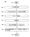
表面テクスチャ化プロセス
加工片104の表面をテクスチャ化するための種々の方法を、図3A、3B、3C、3D、3E、及び3Fに示す。詳述すれば、図3Aは、ステップ301において開始され、加工片104が図1のチャンバ114のような表面テクスチャ化チャンバへ送給されるステップ304以降の一連のプロセスステップ300を示している。図3Bは、図3Aと同じプロセス300を示しているが、テクスチャ化プロセスを実行する前に加工片104を予熱するステップ307が追加されている。図3Cは、図3Aと同じ一連のプロセスステップ300を示しているが、ステップ304の前に加工片104から応力を逃すステップ302と、テクスチャ化プロセスを実行する前に加工片104を予熱するステップ307とが追加されている。図3Dは、図3Aと同じ一連のプロセスステップ300を示しているが、ステップ304の前に加工片104から応力を逃すステップ302が追加されている。予熱ステップ及び応力逃しステップは、テクスチャ化プロセスとは分離したチャンバにおいて、または同一のチャンバにおいて遂行することができる。図3Eは、図3Aと同じ一連のプロセスステップ300を示しているが、ステップ310におけるテクスチャ化プロセスが完了した後に加工片104から応力を逃し、テクスチャ化プロセス中に発生した、またはテクスチャ化プロセスの後に残る何等かの応力を逃すステップ311が追加されている。本発明の他の実施の形態においては、ステップ311を図3B、3C、3D、及び3Fに示す他のプロセスステップ300にも追加し、テクスチャ化プロセスの適用によって加工片内に誘起された残留応力を逃すか、または加工片内に残る応力を除去することができる。図3Fは、図3Aと同じ一連のプロセスステップ300を示しているが、ステップ310が完了した後に加工片を化学的に清浄化するステップ312が追加され、その後のプロセスへの汚染の影響を減少乃至は阻止し、また第2の材料の加工片への付着を改善するようにしている。本発明の他の実施の形態においては、ステップ312を図3B、3C、3D、及び3Eに示す他のプロセスステップ300にも追加し、加工片を使用するであろうその後のプロセスへの汚染の影響を減少乃至は阻止し、また第2の材料の加工片への付着を改善することができる。
Various methods for texturing the surface of the surface
加工片は、一般的には、金属または金属合金のような材料、セラミック材料、ポリマー材料、複合材料、またはそれらの組合わせからなる。一実施の形態においては、加工片は鋼、ステンレス鋼、タンタル、タングステン、チタン、銅、アルミニウム、ニッケル、酸化アルミニウム、窒化アルミニウム、酸化シリコン、炭化シリコン、サファイア(Al2O3)、及びそれらの組合わせからなるグループから選択された材料からなる。一実施の形態においては、加工片は、オーステナイト系ステンレス鋼、鉄・ニッケル・クロム合金(例えば、インコネル(登録商標)合金)、ニッケル・クロム・モリブデン・タングステン合金(例えば、ハステロイ(登録商標))、銅・亜鉛合金、クロム・銅合金(例えば、5%または10%Cr、残りがCu)等のような金属合金からなる。別の実施の形態においては、加工片は石英からなる。加工片は、ポリイミド(Vespel(登録商標))、ポリエーテルエーテルケトン、ポリアリル酸塩(Ardel(登録商標))等のようなポリマーからなることもできる。 The workpiece generally comprises a material such as a metal or metal alloy, a ceramic material, a polymer material, a composite material, or a combination thereof. In one embodiment, the workpiece is steel, stainless steel, tantalum, tungsten, titanium, copper, aluminum, nickel, aluminum oxide, aluminum nitride, silicon oxide, silicon carbide, sapphire (Al 2 O 3 ), and their A material selected from the group consisting of combinations. In one embodiment, the workpiece is austenitic stainless steel, iron-nickel-chromium alloy (eg, Inconel (registered trademark) alloy), nickel-chromium-molybdenum-tungsten alloy (eg, Hastelloy (registered trademark)). , Copper / zinc alloy, chromium / copper alloy (for example, 5% or 10% Cr, the remainder is Cu), and the like. In another embodiment, the workpiece is made of quartz. The workpiece can also be made of a polymer such as polyimide (Vespel®), polyetheretherketone, polyallylate (Ardel®), and the like.
ステップ306においてチャンバ114及びカラム120は約1×10⁻³乃至1×10⁻⁵トルの範囲内の圧力まで排気される。一実施の形態においては、電磁ビームは、抵抗加熱器(図示せず)を使用して陰極106を加熱し、電源(図示せず)を使用して陰極に電流を印加することによって形成される。陰極から脱出した電子は、バイアスカップ116に収集される。陽極に対して負の高電圧電位(以下、加速電圧という)がケーブル122を介して陰極106に印加され、大きさが加速電圧より小さい第2の負電位がバイアスカップ116に印加される。加速電圧は、約50乃至約160kVの範囲内にあることができる。第2の電位は、加工片104へ送給される電子ビームエネルギの大きさを制御するために使用される。
In
電子は陽極108内の孔118を通って移動し、発散し始める。陽極108の下に位置する高速集束コイル110は電子ビームを加工片104上で小さい直径に集束させ、一方高速偏向コイル112A、112Bはビームを磁気的に加工片104の表面の特定の位置に偏向させる。電磁ビーム102を操作するのに十分な磁束を発生させるために、電流が高速集束コイル110と高速偏向コイル112A、112Bとに印加される。高速集束コイル110及び高速偏向コイル112A、112Bを通過した電子ビームは、図3のステップ308に示すように加工片の表面へ供給される。チャンバ114の頂面114Tと加工片104との間の距離が、ビームの作業距離である。一実施の形態におけるこの作業距離は、約50mm乃至約1,000mmであり、好ましくは約200mm乃至約350mmである。
The electrons move through the
図2を参照する。マイクロプロセッサコントローラ200を、集束コイル110及び高速偏向コイル112A、112Bに結合することが好ましい。マイクロプロセッサコントローラ200は、種々のチャンバ及びサブプロセッサのための工業設定に使用することができる何等かの汎用コンピュータプロセッサ(CPU)の一形状であることができる。コンピュータは、ランダムアクセスメモリ、読出し専用メモリ、フロッピー(登録商標)ディスクドライブ、ハードディスク、またはローカルの、または遠隔の何等かの他の形状のディジタル記憶装置のような、何等かの適当なメモリを使用することができる。広く知られているようにしてプロセッサを支援するために、種々の支援回路をCPUに結合することができる。必要に応じてソフトウェアルーチンをメモリ内に格納することも、または遠隔配置されている第2のCPUによって実行させることもできる。
Please refer to FIG. The
ソフトウェアルーチンは、チャンバ114内に加工片104が位置決めされると実行される。ソフトウェアルーチンが実行されると、汎用コンピュータは、チャンバプロセスを遂行するようにチャンバ動作を制御する特定プロセスコンピュータに変換される。代替として、本発明のプロセスは、特定用途向け集積回路または他の型のハードウェア装置としてのハードウェアによって、またはソフトウェア及びハードウェアの組合わせによって遂行させることができる。
The software routine is executed when the
更に図2を参照する。典型的には1組の命令がコンピュータ可読媒体上にエンコードされており、これがコントローラ200へ供給される。命令の実行によって発生した制御信号は、コントローラ200から1またはそれ以上の関数発生器204を通して高速集束コイル110及び高速偏向コイル112A、112Bへ伝えられる。一実施の形態においては、命令は5つの関数発生器204を通して伝えられる。5つの関数発生器の1つは、高速集束のために使用される。2つの関数発生器はビームの主偏向のために使用され、2つの関数発生器がビームの二次偏向のために使用される。関数発生器には、対応する電力増幅器(図示せず)が付属している。命令は、典型的には高速集束コイル110及び高速偏向コイル112A、112Bが電磁ビーム102を操作することを可能にし、加工片104の表面上の特定位置へビームを運動させることによって加工片104の表面上にフィーチャの特定のパターン、間隔、及び特性を作出する。
Still referring to FIG. A set of instructions is typically encoded on a computer readable medium and provided to the
関数発生器204は、さまざまな周波数にわたる信号波形を発生することができる。それにより、コントローラ200が発した信号応じて電子ビーム102の位置及び合焦直径を迅速に調整し、加工片の表面上にフィーチャを迅速に形成することができる。関数発生器204は、コントローラ200と集束コイル110並びに高速偏向コイル112A、112Bとの間の信号の伝達を容易にするために、好ましくは1またはそれ以上の電力増幅器、電源等(図示せず)へ結合されている。
The
図3のステップ310に示すように、電磁ビーム102は、加工片104の表面を横切って走査される。加工片104の表面を横切ってビームを走査させる前に、加工片104を予熱温度まで加熱することができる。予熱温度は、一般的には加工片104を構成している材料に依存する。例えば、加工片104は、加工片104が溶融し、物理的状態を変化させ、または実質的な分解を生じ始める温度より低い予熱温度まで加熱することができる。加工片104は、例えば図1に示す加熱要素150を使用して加熱することができる。また加工片104は、加工片104をテクスチャ化する前に、電子ビームを用いて構成部品を走査することによって加熱することもできる。この予備走査ステップは、テクスチャ化を遂行しようとしている領域を加熱するパターンで電子ビームを表面全体に迅速に移動させることによって遂行することができる。一実施の形態においては、加工片の予熱プロセス中に、電子ビームまたは他のエネルギ源プロセスパラメータ(例えば、焦点距離及びプロセス電力)を変化させる。予熱プロセス中に使用されるプロセスパラメータは、所望予熱温度、加工片の表面を横切って移動させるビームの速度、及び/またはテクスチャ化する前に予熱する加工片材料に依存しよう。
As shown in
一実施の形態においては、テクスチャ化プロセスを遂行する前に加工片を予熱するプロセスは、チャンバ114内の加工片104付近に取り付けられているエネルギ源181を使用することによって達成することができる。典型的なエネルギ源の例は、限定するものではないが、当分野においては公知の放射熱ランプ、誘導加熱器、または赤外型抵抗加熱器を含む。この構成においては、テクスチャ化プロセスが開始される前に、指定された時間にわたって、または加工片が所望の温度に到達するまで、エネルギ源181をターン“オン”させて維持する(ステップ307)。別の実施の形態においては、加工片104をチャンバ114の外部で予熱し(ステップ304の前に完了させる)、テクスチャ化プロセスを遂行する直前にチャンバへ転送することができる。
In one embodiment, the process of preheating the workpiece prior to performing the texturing process can be accomplished by using an
応力逃がしプロセスは、他の先行製造プロセスによって加工片内に生じた残留応力の緩和を原因とする加工片104の歪みを防ぐために、予熱及びテクスチャ化プロセスの前に遂行することもできる。残留応力は、グリットブラスト及び種々の材料形成プロセス(例えばミーリング、引抜き、焼結、モールディング等)のようなさまざまな先行製造動作によって発生し得る。応力逃がしの方法またはプロセスは部品組立及び/または製造の分野においては公知であり、処理方策は材料の型、使用される形成プロセスの量及び型、及び加工片歪みに対する公差に依存しよう。
The stress relief process can also be performed prior to the preheating and texturing process to prevent distortion of the
図4を参照する。ビーム102は、集束コイル110及び高速偏向コイル112A、112Bを通って走行する。コントローラ200から関数発生器204を通して送られる信号の本質に依存して、ビーム102は、加工片104の表面の特定部分を横切って走査される。これによって、加工片104の表面上に複数のフィーチャ500が形成される。フィーチャ500は、特定の幾何学的パターンであることができる。一実施の形態においては、テクスチャ化プロセス中に衝突する電磁ビーム102に対して加工片104を運動させる。加工片104は、電磁ビーム102に対して、例えば約1m/分乃至約1.7m/分の範囲の走行速度で運動させることができる。一実施の形態においては、電磁ビーム102の照射中に、加工片を1またはそれ以上の回転軸を中心として回転させる。回転軸は、例えば、入射ビームに直角または平行であることができる。加工片のサイズまたは形状によっては加工片を物理的に運動または回転させることができないかも知れず、その場合には加工片104を横切って電磁ビーム102を運動させて所望のテクスチャを形成することができる。
Please refer to FIG.
一般的に言えば、電磁ビーム102が電子ビーム、イオンビーム、または電気アークによって生成される場合には、電流が加工片104へ流れる。電磁ビーム102が電子ビームである場合には、電流は約15乃至約50ミリアンペア(mA)、好ましくは15乃至40mAの範囲内にあることができる。電磁ビーム102によって送給されるエネルギは電力密度として定義され、これは加工片の表面上の特定の断面積を横切って送給される平均電力である。一実施の形態においては、電磁ビーム102の平均電力密度は、ビームが導かれる加工片の表面上のある点において、例えば約104W/mm2乃至約105W/mm2の範囲内にあることができる。電磁電磁ビーム102のピーク電力密度は、ビームが導かれる加工片の表面上のある点において、例えば約105W/mm2乃至約107W/mm2の範囲内にあることができる。ピーク電力密度は、与えられた電力設定においてビームがその最大集束(即ち、可能な最小スポットサイズ)にある場合のプロセス設定として定義することができる。加工片の表面上にフィーチャ500を形成させるために必要なエネルギの量は、加工片の吸収効率またはエネルギ転送効率に起因して、エネルギ源の型(例えば、電子ビーム、レーザ等)毎に異なり得ることに注目されたい。
Generally speaking, current flows to the
電磁ビームによって加工片の表面へ送給される電力またはエネルギは、加工片を重大に、または甚だしく歪ませる(例えば、溶融、反り、割れ等)ことを意図してはいない。加工片の重大な、または甚だしい歪みとは、一般的に、テクスチャ化プロセスを遂行したことによって加工片がその意図した目的のために使用できなくなる状態のことをいう。加工片に重大な歪みをもたらすのに必要なエネルギの量は、加工片を構成している材料、テクスチャ化される領域付近の加工片の厚み及び/または質量、加工片の形状(例えば、平坦、円筒形等)、加工片内の残留応力の量、加工片へ送給される実際の電力、加工片の表面上のテクスチャ化されたフィーチャ(フィーチャ500)の密度、及び/または加工片上の任意の点におけるビームの休止(ドエル)時間に依存しよう。一実施の形態においては、テクスチャ化プロセスによって誘起される熱応力に鋭敏な1または複数の薄い加工片に重大な歪みを生じさせないようにするために、以下の諸ステップを遂行することができる。即ち、加工片へ送給されるエネルギを減少させる(加工片の表面上にフィーチャ500を形成させるために使用されないようにする)ために、ビーム移動(もしくはビーム転送)速度を増加させることができ、移動時間中にビームの焦点をぼかすことができ、または移動時間中にビームの電力を減少させることができる。歪みを受け易い加工片(例えば、高い熱膨張を有する幾何学的に平坦な材料等)内の歪みを減少させるために、一実施の形態においては加工片の一方の側のテクスチャ化プロセスによって誘起される応力を補償するために、加工片の両側のテクスチャ化を遂行するテクスチャ化プロセス必要とする。
The power or energy delivered to the workpiece surface by the electromagnetic beam is not intended to severely or severely distort the workpiece (eg, melting, warping, cracking, etc.). Severe or severe distortion of a workpiece generally refers to a condition in which the workpiece has become unusable for its intended purpose as a result of performing the texturing process. The amount of energy required to cause significant distortion to the workpiece is the material that the workpiece is made of, the thickness and / or mass of the workpiece near the textured area, the shape of the workpiece (eg, flat , Cylindrical, etc.), the amount of residual stress in the workpiece, the actual power delivered to the workpiece, the density of the textured features (feature 500) on the workpiece surface, and / or on the workpiece Depend on the beam dwell time at any point. In one embodiment, the following steps can be performed to prevent significant distortion in one or more thin workpieces that are sensitive to thermal stresses induced by the texturing process. That is, the beam movement (or beam transfer) speed can be increased to reduce the energy delivered to the workpiece (so that it is not used to form the
別の実施の形態においては、基体支持具140内の加熱要素150は、テクスチャ化プロセス中に到達する最高温度を低下させるために、テクスチャ化プロセス中に加工片104を冷却するように、及び/または、加工片内の歪みを防ぐまたは減少させるために、テクスチャ化の後の冷却速度を制御できるようになっていることができる。この実施の形態における加熱要素150は、ミシガン州トラバースシティのTEテクノロジー社、またはニューハンプシャー州ナシュアのフェロテック・アメリカ・コーポレーションから販売されているような熱電デバイスで製造することができる。別の実施の形態においては、加工片を基体支持具140へクランプして加工片のたわみを拘束し、テクスチャ化中の加工片の歪みを防ぐことができる。
In another embodiment, the
一般的に言えば、ビームは、加工片の組成に依存して変化するエネルギの空間分布を有している。ビームは、一般的に、中心値の周りで変化するエネルギの空間分布を有しており、それは例えばガウス分布であり得る。他の実施の形態においては、ビームは、非ガウス分布を有することができる。例えば、ビームは、ビーム直径を横切るエネルギの空間分布を有することができ、これはガウス分布よりもビーム直径を横切って実質的により均一である。オーステナイト系鋼のために有用な一実施の形態においては、ビームエネルギのほぼ90%乃至約98%、好ましくは約98%が約0.4mmのビーム直径内に含まれており、残りのエネルギは約0.4mmの直径の外側にあるが、全体的には直径1mm内にある。 Generally speaking, the beam has a spatial distribution of energy that varies depending on the composition of the workpiece. The beam generally has a spatial distribution of energy that varies around a center value, which can be, for example, a Gaussian distribution. In other embodiments, the beam can have a non-Gaussian distribution. For example, the beam can have a spatial distribution of energy across the beam diameter, which is substantially more uniform across the beam diameter than a Gaussian distribution. In one embodiment useful for austenitic steels, approximately 90% to about 98%, preferably about 98% of the beam energy is contained within a beam diameter of about 0.4 mm and the remaining energy is about It is outside the diameter of 0.4 mm, but is generally within 1 mm in diameter.
一実施の形態においては、ビームは、高速偏向コイル112A、112Bは使用するが、集束コイルは使用することなく加工片の表面を横切って走査される。この実施の形態においては、テクスチャ化プロセス中にはビームは集束され続ける。図5Aは、テクスチャ化された加工片104の表面の概要を示す上面図である。ビームは、高速偏向コイル112A、112Bを使用することによって主偏向を受ける。高速偏向コイル112A、112Bは、ビームを種々の参照点Rの近傍に移動させる。主偏向周波数は、約23乃至約32Hzの範囲内にあることができる。参照点Rの近傍に移動させられた後に、ビームは複数の二次偏向を受ける。各二次偏向によって、ビームは、例えば図5AにR’で示す副参照点まで移動させられる。特定の二次偏向を受けたビームは、加工片104の表面と相互作用してその上にフィーチャを形成する。二次偏向周波数は、約400Hz乃至約10kHzの範囲内にあることができる。一実施の形態においては、二次偏向周波数は約2kHz乃至約4kHzの範囲内にある。
In one embodiment, the beam is scanned across the surface of the workpiece using high speed deflection coils 112A, 112B, but no focusing coil. In this embodiment, the beam continues to be focused during the texturing process. FIG. 5A is a top view showing an overview of the surface of the
二次偏向は、フィーチャ500が参照点Rの周囲にパターン520を形成するように、空間的に配列することができる。図5Aに示すパターン520は、線形パターンである。勿論、円形、楕円形、三角形、星形、中心スポットを有する円形を含む他の多くのパターンも可能である。各参照点Rの周りの二次偏向の数は可変であり、例えば約100までであることができる。
The secondary deflections can be spatially arranged such that the
一実施の形態においては、フィーチャ500は、図5Cに示すように六方最密充填(HCP)パターンに配列されており、これは6つの密に配列されたフィーチャ500(A2乃至A7で示す)によって取り囲まれた1つのフィーチャ500(A1で示す)として定義することができる。HCPパターンを繰り返して、加工片の表面全体にフィーチャのアレイを形成させることができる。六方最密充填パターンを使用すると表面上のフィーチャ500の密度が最大となり、その後の蒸着プロセス(後述)中にテクスチャ化された加工片104を使用する場合に、加工片104の表面上に蒸着された材料の付着が改善される。テクスチャ密度は、加工片104上の1cm2の表面積内のフィーチャ500の数として定義され、測定される。テクスチャ密度は、加工片材料、その後のプロセスにおいて蒸着される材料の型、電磁ビームの入射角、及び種々のフィーチャ500のサイズ及び間隔によって変化させることはできるが、一般的には、約1乃至300フィーチャ/cm2、好ましくは約20乃至約260フィーチャ/cm2である。例えば、カリフォルニア州サンタクララのアプライド・マテリアルズ社製の、タンタルのPVD蒸着プロセスに使用されるチタン製品(部品番号0020-46649)は、テクスチャ化された表面全体に約200乃至約260フィーチャ/cm2を含むことができる。更に別の例として、アプライド・マテリアルズ社製の、タンタルまたは窒化タンタルのPVD蒸着プロセスに使用されるアルミニウム製品(部品番号0020-44438)は、テクスチャ化された表面全体に約30乃至約50フィーチャ/cm2を含むことができる。
In one embodiment, the
図5Bは、テクスチャ化された加工片104の表面の拡大上面図である。電磁ビーム102は、ビーム直径504を有している。電磁ビーム102が加工片104の表面と接触する点におけるビーム直径504は、約0.4mm乃至約1mmであり、好ましくは約0.4mmである。ビームは、加工片104の表面上の領域502上に合焦し、休止時間として知られる時間の間、領域502上で合焦し続ける。休止時間中、ビームは加工片104の表面の領域502と相互作用してその上にフィーチャを形成する。
FIG. 5B is an enlarged top view of the surface of the
図5Bに示すように、このようにして形成されたフィーチャは、電磁ビーム102が加工片104の表面と接触する点におけるビーム直径504のサイズと実質的に同一の直径506を有することができる。
As shown in FIG. 5B, the feature formed in this manner can have a
一般的に言えば、ビームの休止時間は、約0.1ミリ秒(ms)乃至約2msの範囲内にあることができる。各二次偏向の間に経過する移動(トランジット)時間は、約1マイクロ秒(μs)乃至50μsであることができる。発明者らは、オーステナイト系鋼に対してこのような短い移動時間を使用すると、あるフィーチャから次のフィーチャへの移動中にビームの焦点をぼかしたり、または電力を減少させたりする必要がないことを見出した。ビーム移動時間中にだけビームに曝される表面は知覚できる程溶融せず、従ってフィーチャはビームが休止する領域内にだけ形成される。休止時間が経過すると、電磁ビーム102は加工片104の表面上の、領域510のような別の領域へ偏向される。一実施の形態においては、フィーチャ500が配置される加工片の領域が幾何学的に薄いか、または脆いことに起因して加工片が歪むのを防ぐために、休止時間を1msより短く(例えば約0.1msに)短縮し、及び/または移動時間を1μsより短く短縮することができる。
Generally speaking, the beam dwell time can be in the range of about 0.1 milliseconds (ms) to about 2 ms. The transit time that elapses between each secondary deflection can be about 1 microsecond (μs) to 50 μs. Inventors use such short travel times for austenitic steels to avoid having to defocus the beam or reduce power while moving from one feature to the next. I found. The surface exposed to the beam only during the beam travel time does not melt appreciably, so the feature is formed only in the region where the beam rests. As the dwell time elapses, the
別の実施の形態においては、集束コイル110は、移動時間中に加工片104の表面に衝突するビームのパワーを減少させるために、焦点を迅速に合わせたり、ぼかしたりするように電磁ビーム102を運動させる。このようにすると、加工片104の表面に送給されるエネルギはより精密に制御されるようになる。上述した方法と同様にして、複数のフィーチャ500が加工片104の表面上に形成される。
In another embodiment, the focusing
複数のフィーチャ500は、凹み、突起、またはそれらの組合わせであることができる。複数のフィーチャ500は、フィーチャ500間の間隔508が実質的に均一であるパターンに配列することができる。図5A、5B、及び5Cには離散したフィーチャ500のパターンを示してあるが、フィーチャ500は互いに接触させ、重ね合わせ、または併合させることができる。1つの可能な重ね合わせデザインの実施の形態を図5Dに示す。別の実施の形態においては、蒸着された薄膜の付着を高める壕または溝を加工片の表面上に形成するために、重ね合わされたフィーチャ500のアレイを形成することも可能である。
The plurality of
図6は、ビーム直径606を有する電磁ビーム102のような電磁ビームと接触した加工片104の表面の一実施の形態の概要断面図である。図示のように、電磁ビーム102は入射角610で表面に当たる。入射角610は、加工片104の表面に垂直な線610Aと、電磁ビーム102に平行な線610Bとがなす角度として定義される。入射角は、約−45°乃至約45°、好ましくは約−30°乃至30°の範囲内にあることができる。換言すれば、入射角は線610Aに対して測定して、約45°以内にあることができる。フィーチャ500は一般的に凹み602を含み、電磁ビーム102に曝されると突起604が形成される。
FIG. 6 is a schematic cross-sectional view of one embodiment of the surface of a
この入射角でビームを偏向させると、テクスチャ化プロセス中に表面から分離する材料がカラム120内の種々のハードウェア構成部品を見通せなくなるので、ハードウェアの寿命またはハードウェアの保守サイクルを改善する効果も得られる。カラム120に対するビームの偏向が、カラム120内をイオンが上昇して陰極106及びカラム120内の他の構成部品を損傷させるのを最小に、好ましくは阻止することができる。
By deflecting the beam at this angle of incidence, the material that separates from the surface during the texturing process will not be able to see the various hardware components in the
発明者らは、これらのフィーチャ500が形成される理由を何れか1つの特定の説明に固執することは望まないが、加工片104の表面及び内部の材料が高温に、ある場合には加工片104を構成している材料の沸騰温度より高い温度まで加熱されるものと考えている。加工片の部分が急速に加熱されると材料が外部へ放出される。そのため、材料が放出された位置に凹み602が形成され、また放出された材料が蒸着した位置に突起604が形成される。
The inventors do not want to stick to any one particular explanation why these
凹み602は、表面622を有することを特徴としている。凹み602は、加工片104の頂面620から凹み602の底までの垂直距離として定義される深さ612を有し、この深さは約0.001インチ乃至約0.060インチの範囲である。凹みは、約0.005インチ乃至約0.100インチ、好ましくは約0.008インチ乃至約0.089インチの範囲の表面直径614を有している。凹みは、内部直径616を有している。内部直径616は、表面622上の加工片104の頂面620に平行な2つの点間の最大距離として定義される。一実施の形態においては、凹みは、表面直径614より大きい内部直径616を有している。別の実施の形態においては、凹みは、表面直径614より小さい内部直径616を有している。一実施の形態においては、突起604は、約0.002インチ乃至約0.060インチ、好ましくは約0.002インチ乃至約0.046インチの範囲の高さを有している。アルミニウム加工片(アプライド・マテリアルズ社製部品番号0020-44438)内に形成されたフィーチャ500の寸法の範囲の例では、表面直径614は約0.029インチ乃至約0.089インチであり、高さ618は約0.017インチ乃至約0.046インチであり、そして深さ612は約0.023インチ乃至約0.036インチである。チタン加工片(部品番号0020-46649)内に形成されたフィーチャ500の寸法の典型的な範囲の別の例では、表面直径614は約0.012インチ乃至約0.031インチであり、高さ618は約0.002インチ乃至約0.004インチであり、そして深さ612は約0.006インチ乃至約0.011インチである。
The
図6は、凹み602及び2つの突起604を含む特定のフィーチャの形成を示しているが、凹みだけ、または突起だけの形成、または凹みと突起との変化する比及び組合わせも本発明の範囲内にある。更に、凹みは、変化する形状、深さ、表面直径、及び内部直径を有することができる。同様に、突起も、変化する形状及び高さ、並びに加工片表面との変化する接触角を有することができる。突起及び凹みは、互いに接触し、重なり合い、または併合していることも、または互いに離間していることもできる。一実施の形態においては、突起間の、または凹み間の間隔は、約0.02インチより小さい。
Although FIG. 6 shows the formation of a particular feature including a
一実施の形態においては、ビームは、加工片の表面上に投射された電磁ビームの静的形状とは異なるフィーチャを形成するために、ビームの休止時間中に小さく偏向させることができる。休止時間中にビームを偏向させることによって得られる望ましい形状は、例えば、星形、長円形、菱形、三角形、矩形、五角形、六角形、または他の多辺形を含むことができる。 In one embodiment, the beam can be deflected small during the beam downtime to form features that differ from the static shape of the electromagnetic beam projected onto the surface of the workpiece. Desirable shapes obtained by deflecting the beam during the downtime can include, for example, a star, oval, diamond, triangle, rectangle, pentagon, hexagon, or other polygon.
一実施の形態においては、電磁ビーム102による表面テクスチャ化処理の後に、硬い粒子の流れを加工片104にスプレーする(“ビード吹き付け”)。硬い粒子は、例えば、酸化アルミニウム、ガーネット(ざくろ石)、炭化シリコン、または酸化シリコンからなることができ、また粒子サイズは約24乃至約80グリット(約535ミクロン乃至約192ミクロン)であることができる。典型的に“ビード吹き付け”プロセスは、約5乃至約70psiの送給圧で遂行される。硬い粒子は、ノズルからスプレーすることができ、また乾式で、または水性スラリー組成の一部としてスプレーすることもできる。一般的に言えば、ビード吹き付け処理によりもたらされる加工片104の表面粗さは、電磁ビーム102を使用して発生させた粗さよりも細かい。またビード吹き付け処理は、何等かのゆるく付着した材料(例えば、テクスチャ化プロセスによって形成された突起)を除去する。ビード吹き付け処理によって形成される粗さは、材料がその上に蒸着された時にテクスチャ化された構成部品の保持性または接着性を増加させる。更に、ビード吹き付けは、使用後の構成部品を清浄化するために使用することができる。ビード吹き付け処理は、構成部品上に蒸着した材料を除去し、蒸着プロセスの前に初めに構成部品に施された表面仕上げを復元する。
In one embodiment, after surface texturing with the
別の実施の形態においては、加工片104は、表面テクスチャ化プロセスの後に化学的に粗くされる。“化学的に粗くする”という表現は広義に解釈すべきであり、限定するものではないが、構成部品表面の化学的エッチング、構成部品表面の電気化学的エッチング、またはそれらの組合わせを含む。化学的に粗くするプロセスは、上述したビード吹き付けプロセスと同様に、蒸着した薄膜の加工片104への付着を改善するのを援助できる粗い表面を形成するために使用される。加工片104の表面を化学的に粗くする方法は加工片を構成している材料に依存し、化学清浄、冶金、及び化学加工の分野に精通していれば容易に理解できよう。化学的エッチングとは、限定するものではないが、一般的に化学的活性を使用することによって加工片の表面から材料を除去するプロセスのことをいう。使用することができる典型的な薬品の例は、硫酸(H2SO4)、硝酸(HNO3)、塩酸(HCl)またはそれらの組合わせのような酸を含む水性酸性溶液、または水酸化カリウム(KOH)、水酸化アンモニア(NH4OH)、またはそれらの組合わせのような薬品を含む水性塩基性溶液であることができる。別の実施の形態においては、加工片の表面の化学的エッチングプロセスは、ドライエッチング(プラズマエッチング)プロセスを使用して遂行することができる。ドライエッチングは、一般的に言えば、加工片表面と相互作用し、究極的に該表面から材料を除去する反応性ガス種にエネルギを与える、または解離させるプラズマを発生するプロセスである。電気化学的エッチングとは、一般的に言えば、限定するものではないが、電解質溶液内に浸漬され陰極として働く別の要素に対し、加工片に陽極バイアスを印加することによって加工片表面から材料を除去するプロセスのことである。本発明から利益を得ることができる電気化学的エッチングプロセスの例が、2001年7月27日付米国特許出願第09/918,683号(代理人ドケット番号5431)“電気化学的に粗くしたアルミニウム製半導体処理装置表面”に開示されているので参照されたい。
In another embodiment, the
粒子汚染を減少させる方法
本発明の別の実施の形態においては、プロセスチャンバ内の汚染を減少させる方法が提供される。一実施の形態においては、本方法は、プロセスチャンバへ供給された基体の汚染を減少させる。一般的に言えば、チャンバは、チャンバの内部表面上に、またはチャンバ内の諸構成部品の表面上に材料が凝縮し易い何等かの囲まれた、または部分的に囲まれたチャンバであることができる。一実施の形態においては、チャンバは、基体処理チャンバである。このチャンバは、半導体基体またはガラスパネルの真空処理に適するチャンバである。ウェハー処理チャンバは、例えば蒸着チャンバであることができる。代表的な蒸着チャンバは、スパッタリングチャンバ、物理蒸着(PVD)チャンバ、及びイオン金属プラズマ(IMP)チャンバ、化学蒸着(CVD)チャンバ、エッチングチャンバ、分子線エピタキシー(MBE)チャンバ、原子層蒸着(ALD)チャンバ、その他を含む。チャンバは、例えばプラズマエッチングチャンバのような、エッチングチャンバであることもできる。他の適当なプロセスチャンバの例は、イオン注入チャンバ、焼鈍チャンバ、その他の炉チャンバを含む。好ましい実施の形態においては、チャンバは、基体が1またはそれ以上の気相材料に曝される基体プロセスチャンバである。
Method for reducing particle contamination In another embodiment of the present invention, a method for reducing contamination in a process chamber is provided. In one embodiment, the method reduces contamination of the substrate supplied to the process chamber. Generally speaking, the chamber is any enclosed or partially enclosed chamber on which the material is likely to condense on the interior surface of the chamber or on the surfaces of the components within the chamber. Can do. In one embodiment, the chamber is a substrate processing chamber. This chamber is a chamber suitable for vacuum processing of a semiconductor substrate or a glass panel. The wafer processing chamber can be, for example, a deposition chamber. Typical deposition chambers include sputtering chambers, physical vapor deposition (PVD) chambers, and ion metal plasma (IMP) chambers, chemical vapor deposition (CVD) chambers, etching chambers, molecular beam epitaxy (MBE) chambers, atomic layer deposition (ALD). Includes chambers and others. The chamber can also be an etching chamber, such as a plasma etching chamber. Examples of other suitable process chambers include ion implantation chambers, annealing chambers, and other furnace chambers. In a preferred embodiment, the chamber is a substrate process chamber in which the substrate is exposed to one or more vapor phase materials.
図7は、以下に説明する実施の形態を使用して汚染を減少させることができるスパッタリング反応器700の簡易化断面図である。反応器700は、真空チャンバ716、及び頂面736Aを有する基体支持具736を含む。基体支持具736は、例えば、静電チャックであることができる。反応器700は更に、シールド組立体718及びエレベータシステム732を含む。基体720(例えば、半導体ウェハー)は、基体支持具736の頂面736A上に位置決めされる。図示配列においては、基体支持具736は、複数のねじによって普通の垂直に運動可能なエレベータシステム732に取り付けられている。明瞭化のために、ガス入口マニホルド、及び/または真空ポンプのような幾つかのハードウェアは省略してある。
FIG. 7 is a simplified cross-sectional view of a sputtering
図示の真空チャンバ716は、円筒形のチャンバ壁714、及びこのチャンバ壁の頂部に取り付けられている支持リング712を含んでいる。チャンバの上部は、内部表面706Aを有するターゲット板706によって閉じられている。ターゲット板706は、ターゲット板706と支持リング712との間に配置されている環状絶縁体710によってチャンバ壁714から電気的に絶縁されている。一般的には、チャンバ716内の真空の完全性を確保するために、真空シール用のOリング(図示せず)が絶縁体710の上下に使用される。ターゲット板706は、蒸着種になる材料で製造することも、または蒸着種の被膜を含むこともできる。スパッタリングプロセスを促進するために、電源702がターゲット板706に接続されている。
The illustrated
基体支持具736は、基体720をチャンバ716内に保持し、支持する。基体支持具736は、支持ボディ738内に埋込まれた1またはそれ以上の電極734を含むことができる。電極は電極電源704からの電圧によって駆動され、電圧の印加に応答して基体720をチャックの支持表面にクランプする。チャックボディは、例えばセラミック材料からなることができる。
The
壁状の円筒形シールド部材742が、支持リング712に取り付けられている。シールド部材742を円筒形状にしてあるのは、シールド部材をチャンバ及び/または基体の形状に合わせたに過ぎない。勿論、シールド部材742は、如何なる形状であることもできる。部品の例を挙げれば、カリフォルニア州サンタクララのアプライド・マテリアルズ社から入手可能な0020-45544、0020-47654、0020-BW101、0020-BW302、0190-11821、0020-44375、0020-44438、0020-43498、0021-JW077、0020-19122、0020-JW096、0021-KS556、0020-45695を含むことができる。
A wall-shaped
シールド組立体718は、シールド部材742の他に環状蒸着リング730を更に含んでいる。リング730の内径は、リングが基体と接触することなく基体720の縁の上に周縁的にフィットするように選択されている。この環状蒸着(シャドウ)リングは位置合わせリング728上に載っており、位置合わせリング728は基体支持具736から伸びているフランジ(図示せず)によって支持されている。更に、物理蒸着(PVD)に使用されているクランプリングのような他の構成部品を、上述した、そして意図する応用に使用されるプロセスに従ってテクスチャ化することができる。環状蒸着(シャドウ)リング、及び/またはクランプリングの例は、カリフォルニア州サンタクララのアプライド・マテリアルズ社から入手可能な0020-43171及び0020-46649を含む。
The
スパッタ蒸着プロセス中にプロセスガスがチャンバへ供給され、電力がターゲット板706に印加される。プロセスガスは点弧されてプラズマになり、ターゲット板706に向かって加速される。それによってプロセスガスはターゲット板から粒子を追い出し、粒子は基体720上に蒸着して基体上に蒸着された材料の被膜を形成する。
During the sputter deposition process, process gas is supplied to the chamber and power is applied to the
シールド組立体718は、プラズマ及びスパッタされた粒子を概ね反応ゾーン777内に閉じ込めるが、必然的に、初めはプラズマまたはガス状状態のスパッタされた粒子はチャンバの種々の内側表面上に凝縮する。例えば、スパッタされた粒子は、シールド組立体718の内側表面718A上に、ターゲット板706の内側表面706A上に、支持リング712の内側表面712A上に、蒸着リング730の内側表面730A上に、そしてチャンバのその他の内側表面上に凝縮することができる。更に、基体支持具736の頂面736Aのような他の表面も蒸着シーケンス中に、またはそれらの間に汚染され始める。
The
一般的に言えば、“内側表面”とは、チャンバ716との界面を有する何等かの表面のことである。チャンバ構成部品とは、プロセスチャンバ内に完全に、または部分的に収容されている何等かの取り外し可能な要素のことである。チャンバ構成部品は、真空チャンバ構成部品、即ち、例えばチャンバ716のような真空チャンバ内に配置されているチャンバ構成部品であることができる。チャンバ構成部品の内側表面上に形成される凝縮された物質は、一般的には、限定された接着性だけしか有しておらず、構成部品から解放されて基体720を汚染し得る。
Generally speaking, an “inner surface” is any surface that has an interface with the
凝縮した異物がプロセスチャンバ構成部品から分離する傾向を減少させるために、例えば、シールド組立体718、ターゲット板706、支持リング712、蒸着リング730、コイル(図示せず)、コイル支持具(図示せず)、蒸着コリメータ(図示せず)、支持ボディ(ペデスタル)738、位置合わせリング728、シャッタディスク(図示せず)、または基体支持具736のようなチャンバ構成部品が、例えば装置100の作業チャンバ114のようなテクスチャ化チャンバへ供給される。
To reduce the tendency of condensed foreign matter to separate from process chamber components, for example,
図8を参照する。一連のステップ800は、ステップ802から開始されてステップ804へ進み、1またはそれ以上のチャンバ構成部品の表面を横切って電磁エネルギのビームが走査され、それらの上に複数のフィーチャを形成する。これらのフィーチャは、凹み、突起、またはそれらの組合わせであることができる。このようにしてチャンバ構成部品の表面上に形成されたフィーチャの本質は、前述した加工片104と同様である。一般的に言えば、ステップ804は、図3A、3B、3C、3D、3E、及び3Fに関して説明したステップ301乃至314を包含している。
Please refer to FIG. The series of
代替実施の形態においては、本方法は更に、電磁ビーム102によって表面上にフィーチャ500を形成した後に、プロセス構成部品、即ち加工片の表面を粗くするステップを含む。フィーチャ500を形成した後の“ビード吹き付け”プロセス、または化学的に粗くするプロセスのような加工片の表面を粗くするプロセスは、表面テクスチャ化処理によって形成された凹み602の表面622及び突起604の表面がかなり滑らか(約64マイクロインチの表面粗さ(Ra))であるので、蒸着された材料の加工片への付着を改善することができる。テクスチャ化処理によって得られる滑らかな表面は、テクスチャ化プロセス中に発生する溶融表面に作用する表面張力によってもたらされるものと考えられる。蒸着された材料内に見出される内因性応力(例えば、結晶欠陥、積層欠陥等)、及び/または外因性応力(例えば、加工片と蒸着された材料との間の温度差、熱膨張の不一致等)が蒸着された材料の曲がり及び/または破壊をもたらし得るから、“ビード吹き付け”プロセス、または化学的に粗くするプロセスによって表面を粗くすることは重要である。蒸着された材料の曲がりまたは破壊は粒子を生成し得るから、基体720の汚染に連なり得る。本発明の表面を粗くするステップを追加することにより、蒸着された材料の加工片への接着性を、局所化された機械的付着または結合によって改善するのを援助する。一実施の形態においては、チャンバ構成部品または加工片の表面はステップ804におけるテクスチャ化処理の後に、構成部品の表面に硬い粒子の流れを吹き付ける(“ビード吹き付け”)ことによって更に粗くされる。硬い粒子は、例えば、酸化アルミニウム、ガーネット、酸化シリコン、または炭化シリコンからなることができ、また粒子サイズは約24乃至約80グリットであることができる。典型的には、“ビード吹き付け”プロセスは、約5乃至約70psiの送給圧で遂行される。部品にビードを吹き付けるプロセスは、テクスチャ化プロセスから残された軽く付着した材料を除去する効果をも有している。
In an alternative embodiment, the method further includes roughening the surface of the process component, ie, the workpiece, after forming the
本発明の別の実施の形態においては、プロセスキット構成部品(即ち、加工片)は、テクスチャ化された後に化学的に清浄化される。半導体製造におけるデバイスの歩留まりを向上させるためには厳格な清潔さが要求されるから、処理中に粒状化、分解、気化、またはプロセス構成部品から分離し得る何等かの材料を最小化しなければならない。テクスチャ化プロセスの後に見出される幾つかの典型的な汚染源は、例えば、電磁ビームによる加熱が局部的であることを原因としてプロセス構成部品の材料が“噴出”することによって生じた軽く付着した材料、プロセス構成部品の取扱いからの汚染、及び/またはチャンバのテクスチャ化、ビード吹き付け、応力逃し、または化学的に粗くすることによる何等かの汚染を含み得る。典型的な清浄化プロセスは、例えば、苛性エッチング/脱脂ステップ、DI水中洗浄、プロセス構成部品の表面層内の、または表面層上の汚染物を除去するための酸または塩基溶液中エッチング、高圧DI水洗浄、超音波またはメガソニックDI洗浄、及び真空炉または窒素ブロー乾燥のステップを含むことができる。半導体製造におけるデバイスの歩留まりを向上させるために必要な清浄化要求は、UHV化学清浄化及び/または半導体製造の分野に精通していれば理解することができよう。 In another embodiment of the present invention, the process kit component (ie, workpiece) is chemically cleaned after being textured. Because strict cleanliness is required to improve device yield in semiconductor manufacturing, any material that can be granulated, decomposed, vaporized, or separated from process components during processing must be minimized. . Some typical sources of contamination found after the texturing process are, for example, lightly adhering materials resulting from the “spouting” of process component materials due to localized heating by the electromagnetic beam, Contamination from handling of process components and / or any contamination by chamber texturing, bead spraying, stress relief, or chemical roughening may be included. Typical cleaning processes include, for example, caustic etching / degreasing steps, DI water cleaning, etching in acid or base solutions to remove contaminants in or on the surface layer of process components, high pressure DI Water cleaning, ultrasonic or megasonic DI cleaning, and vacuum furnace or nitrogen blow drying steps can be included. The cleaning requirements necessary to improve device yield in semiconductor manufacturing can be understood by those familiar with the field of UHV chemical cleaning and / or semiconductor manufacturing.
一実施の形態においては、清浄化プロセスは、テクスチャ化プロセスステップの全てが完了した後に、しかし構成部品をプロセスチャンバ内に配置するステップの前に遂行される。従って、この実施の形態は、プロセスチャンバ内のプロセス構成部品を使用する前に、全ての汚染を確実に除去することを援助する。別の実施の形態においては、清浄化プロセスはビード吹き付けプロセスの後だけに遂行され、テクスチャ化プロセスの後に残された何等かの汚染、取扱いによる汚染、及びビード吹き付け後の残留粒子を除去する。更に別の実施の形態においては、プロセス構成部品がきれいな環境内で取扱われ、且つパッケージングまたはプロセスチャンバへ送給される前にDI水内で洗浄されることを条件に、テクスチャ化プロセスを遂行する前に構成部品を清浄化することが可能である。 In one embodiment, the cleaning process is performed after all of the texturing process steps are completed, but before the step of placing the components in the process chamber. Thus, this embodiment helps to ensure that all contamination is removed before using process components in the process chamber. In another embodiment, the cleaning process is performed only after the bead spraying process to remove any contamination left after the texturing process, handling contamination, and residual particles after bead spraying. In yet another embodiment, the texturing process is performed provided that the process components are handled in a clean environment and cleaned in DI water before being delivered to the packaging or process chamber. It is possible to clean the components before doing so.
ステップ806において、1またはそれ以上のチャンバ構成部品が、例えばスパッタリング反応器700内のチャンバ716のようなプロセスチャンバ内に位置決めされる。ステップ808に示すように、反応器700内の基体720上にスパッタされた層を形成するようなプロセスシーケンスが反応器内で開始される。
In
以上の説明は、スパッタリング反応器内の汚染を減少させる方法を詳述しているが、如何なる数の異なる型のプロセスチャンバ内の汚染を減少させる方法の使用も本発明の範囲内にある。本発明は、材料が凝縮し得る内部表面を有する如何なるプロセスチャンバにも適用可能である。プロセスチャンバから取り外すことができ且つ装置100のようなテクスチャ化装置内に配置することができる部分的に、または完全にプロセスチャンバ内にある如何なる構成部品も、本発明の方法を使用して処理するのに適している。
Although the above description details a method for reducing contamination in a sputtering reactor, the use of a method for reducing contamination in any number of different types of process chambers is within the scope of the present invention. The present invention is applicable to any process chamber having an internal surface on which material can condense. Any component that is partly or fully within the process chamber that can be removed from the process chamber and placed in a texturing apparatus such as
本方法は、加工片、基体、またはそれに蒸着された層に、蒸着、エッチング、加熱、またはそれ以外に変更するように設計されているプロセスチャンバ内の汚染を減少させるために使用することができる。一実施の形態においては、本方法は、チタン、窒化チタン、タンタル、タングステン、または窒化タンタルの層のような耐熱金属または耐熱金属化合物の層を、基体上にスパッタ蒸着させるように設計されているチャンバ内の汚染を減少させるために使用される。本発明の他の類似実施の形態においては、本テクスチャ化方法を分子線エピタキシー(MBE)、原子層蒸着(ALD)、化学蒸着(CVD)、またはドライエッチングプロセス等における汚染を減少させるために使用することができる。テクスチャ化プロセスを必要とし得る構成部品は、一般的に、処理サイクル中に(蒸着または清浄化プロセス中に)ある量の蒸着を受け、その蒸着された薄膜が直接的に、または間接的に基体を汚染する傾向を有しているような構成部品を含む。カリフォルニア州サンタクララのアプライド・マテリアルズ社から入手可能なMxP+、Super-e、またはeMaxエッチングシステムのような非スパッタリング反応器においてテクスチャ化を必要とする典型的な構成部品の例は、0040-41188、0040-41189、0021-15694、0040-45966、0040-44917、0020-17482、0020-07569、0020-07570、0020-07571、0020-07567、及び0020-07568である。 The method can be used to reduce contamination in a process chamber that is designed to modify deposition, etching, heating, or otherwise on a workpiece, substrate, or layer deposited thereon. . In one embodiment, the method is designed to sputter deposit a layer of refractory metal or refractory metal compound, such as a layer of titanium, titanium nitride, tantalum, tungsten, or tantalum nitride, onto a substrate. Used to reduce contamination in the chamber. In other similar embodiments of the invention, the texturing method is used to reduce contamination in molecular beam epitaxy (MBE), atomic layer deposition (ALD), chemical vapor deposition (CVD), or dry etching processes. can do. Components that may require a texturing process generally undergo a certain amount of deposition during the processing cycle (during the deposition or cleaning process) and the deposited thin film is directly or indirectly substrate Components that have a tendency to contaminate. Examples of typical components that require texturing in non-sputtering reactors such as the MxP +, Super-e, or eMax etching systems available from Applied Materials, Inc. of Santa Clara, California are 0040-41188 , 0040-41189, 0021-15694, 0040-45966, 0040-44917, 0020-17482, 0020-07569, 0020-07570, 0020-07571, 0020-07567, and 0020-07568.
別の実施の形態においては、ステップ808の後に1またはそれ以上のチャンバ構成部品がプロセスチャンバから取り外され、テクスチャ化された表面に付着し得る凝縮した異物の除去プロセスが開始される。
In another embodiment, after
凝縮した異物の除去は、1またはそれ以上のプロセスチャンバ構成部品の表面に、硬い粒子の流れを吹き付けることによって達成することができる。硬い粒子は、例えば、酸化アルミニウム、ガーネット、酸化シリコン、または炭化シリコンからなることができ、また約24乃至約80グリットの粒子サイズを有することができる。好ましいことには、構成部品の表面上のテクスチャ(即ち、凹み及び突起)を実質的に変更することなく、異物を除去するには、この吹き付けで十分である。 The removal of condensed foreign matter can be accomplished by blowing a stream of hard particles onto the surface of one or more process chamber components. The hard particles can comprise, for example, aluminum oxide, garnet, silicon oxide, or silicon carbide, and can have a particle size of about 24 to about 80 grit. Preferably, this spraying is sufficient to remove foreign material without substantially changing the texture (ie, dents and protrusions) on the surface of the component.
別の実施の形態においては、1またはそれ以上のプロセスチャンバ構成部品の表面上に凝縮した異物を除去するために、該表面を化学流体処理する。化学流体処理は、例えば、脱脂用組成、水酸化ナトリウム、過マンガン酸カリウム、水酸化カリウム、水酸化アンモニウム、過酸化水素、硝酸、フッ化水素酸、塩酸、及びそれらの組合わせのような薬品に表面を浸漬させるか、またはこれらの薬品を表面に吹き付けることからなることができる。 In another embodiment, the surface is treated with a chemical fluid to remove foreign matter condensed on the surface of one or more process chamber components. Chemical fluid treatment includes chemicals such as degreasing compositions, sodium hydroxide, potassium permanganate, potassium hydroxide, ammonium hydroxide, hydrogen peroxide, nitric acid, hydrofluoric acid, hydrochloric acid, and combinations thereof. The surface can be immersed in or sprayed with these chemicals.
この化学流体処理は、硬い粒子の吹き付けに加えて、またはその代わりに使用することができる。代替として、テクスチャ化された表面から異物を除去する他の方法も企図される。好ましいことには、化学処理は、テクスチャ化プロセス中に形成された凹みのマクロ粗さを減少させることがない。それによって、構成部品をチャンバ内へ再配置し、表面上に凝縮する物質のために再び高められた接着性を提供することができる。 This chemical fluid treatment can be used in addition to or instead of spraying hard particles. Alternatively, other methods of removing foreign material from the textured surface are also contemplated. Preferably, the chemical treatment does not reduce the macro roughness of the dents formed during the texturing process. Thereby, the components can be repositioned into the chamber and again provide increased adhesion due to the material condensing on the surface.
本発明の一実施の形態においては、テクスチャ化プロセスは、加工片の表面上に突起を形成するために使用できる例えばアーク溶接プロセス、MIG溶接プロセス、MBEプロセス、または他の類似プロセスによって、類似組成の材料を加工片へ追加することをも含むことができる。追加された材料を確実に付着させるためには、プロセスを真空チャンバ内において、非酸化(例えば、無酸素)環境内において遂行する、及び/または、加工片を材料の融点付近の温度まで加熱する必要があり得る。従って、突起を形成させるために材料を追加するということは、蒸着された薄膜の加工片への付着を増進させることを意味する。この実施の形態を、図3A乃至3Fのステップ310、及び図8のステップ804と置換するか、またはそれに追加できることを構想している。 In one embodiment of the present invention, the texturing process can be used to form protrusions on the surface of the workpiece, such as by arc welding process, MIG welding process, MBE process, or other similar processes. Adding to the workpiece may also be included. To ensure that the added material is deposited, the process is performed in a non-oxidizing (eg, oxygen-free) environment in a vacuum chamber and / or the workpiece is heated to a temperature near the melting point of the material. There may be a need. Thus, adding material to form protrusions means increasing adhesion of the deposited thin film to the workpiece. It is envisioned that this embodiment can be substituted for or added to step 310 of FIGS. 3A-3F and step 804 of FIG.
以上に、本発明の教示を組入れた幾つかの好ましい実施の形態を詳細に説明したが、当業者ならば、これらの教示を組入れた他の多くの実施例を容易に考案できるであろう。 Although several preferred embodiments incorporating the teachings of the present invention have been described in detail above, those skilled in the art can readily devise many other embodiments incorporating these teachings.
100 表面テクスチャ化装置
102 電磁(電子)ビーム
104 加工片
106 陰極
108 陽極
112 高速偏向コイル
114 作業チャンバ
116 バイアスカップ
118 孔
120 カラム
122 高電圧ケーブル
124 ポンプ
126 弁
128、132 分離弁
130 真空ポンプ
140 作動手段
150 加熱要素
181 エネルギ源
200 マイクロプロセッサコントローラ
204 関数発生器
500 フィーチャ
502 加工片表面上の領域
504 ビーム直径
508 フィーチャ間の間隔
510 フィーチャのパターン
602 凹み
604 突起
606 ビーム直径
610 入射角
612 凹みの深さ
614 凹みの表面直径
616 凹みの内部直径
618 突起の高さ
620 加工片の頂面
622 凹みの表面
700 スパッタリング反応器
702 電源
704 電極電源
706 ターゲット板
710 絶縁体
712 支持リング
714 チャンバ壁
716 真空チャンバ
718 シールド組立体
720 基体
728 位置合わせリング
730 蒸着リング
732 エレベータシステム
734 電極
736 基体支持具
738 支持ボディ
742 シールド部材
777 反応ゾーン
DESCRIPTION OF
Claims (47)
前記表面上に凹みと突起とを有する複数のフィーチャを形成させるため、前記構成部品の表面を横切って前記構成部品の表面に垂直な線に対して0〜45°の入射角で電磁ビームを走査させるステップと、
前記構成部品の表面及び前記フィーチャを粗くするステップと、
を含み、前記凹みは表面直径より大きい内部直径を有することを特徴とする方法。 A method of texturing a surface of a component used in a semiconductor process chamber, comprising:
Scanning the electromagnetic beam at an incident angle of 0-45 ° across the surface of the component and perpendicular to the surface of the component to form a plurality of features having indentations and protrusions on the surface Step to
Roughening the surface of the component and the features;
And the recess has an internal diameter that is greater than a surface diameter.
テクスチャ化チャンバを10-3トル乃至10-5トルの範囲の圧力までポンプするステップと、
50乃至160キロボルトの加速電圧において、15乃至50ミリアンペアの電子ビーム電流の電子ビームを前記構成部品の表面を横切って前記構成部品の表面に垂直な線に対して0〜45°の入射角で走査させ、前記表面上に凹みと突起とを有する複数のフィーチャを形成させるステップと、
前記構成部品の表面及び前記フィーチャを粗くするステップと、
を含み、前記凹みは表面直径より大きい内部直径を有することを特徴とする方法。 A method of texturing a surface of a component used in a semiconductor process chamber, comprising:
Pumping the texturing chamber to a pressure in the range of 10 −3 Torr to 10 −5 Torr;
Scanning an electron beam with an electron beam current of 15-50 milliamps at an acceleration voltage of 50-160 kilovolts across the surface of the component at an incident angle of 0-45 ° with respect to a line perpendicular to the surface of the component Forming a plurality of features having indentations and protrusions on the surface;
Roughening the surface of the component and the features;
And the recess has an internal diameter that is greater than a surface diameter.
1またはそれ以上の表面を有するボディと、
前記表面上に形成されている複数のフィーチャと、
を含み、
前記フィーチャは前記プロセスチャンバ構成部品の表面を横切って前記構成部品の表面に垂直な線に対して30〜45°の入射角で電磁エネルギのビームを走査させたことによって形成されており、前記形成されたフィーチャは凹み、突起、及びそれらの組合わせからなるグループから選択され、
前記表面は、前記表面上に複数のフィーチャが形成された後に、化学的に粗くされ、前記凹みは表面直径より大きい内部直径を有することを特徴とするプロセスチャンバ構成部品。 A process chamber component for use in a process chamber comprising:
A body having one or more surfaces;
A plurality of features formed on the surface;
Including
The features are formed by scanning a beam of electromagnetic energy across the surface of the process chamber component at an angle of incidence of 30-45 ° with respect to a line perpendicular to the surface of the component. The selected features are selected from the group consisting of indentations, protrusions, and combinations thereof;
The process chamber component, wherein the surface is chemically roughened after a plurality of features are formed on the surface, and the recess has an internal diameter greater than the surface diameter.
1またはそれ以上の表面を有するボディと、
前記表面上に形成されている複数のフィーチャと、
を含み、
前記フィーチャは前記プロセスチャンバ構成部品の表面を横切って前記構成部品の表面に垂直な線に対して0〜45°の入射角で電磁エネルギのビームを走査させたことによって形成されており、前記形成されたフィーチャは凹み、突起、及びそれらの組合わせからなるグループから選択され、
前記構成部品は、前記プロセスチャンバ構成部品の表面を横切って電磁ビームを走査させる前に、応力除去され、前記凹みは表面直径より大きい内部直径を有することを特徴とするプロセスチャンバ構成部品。 A process chamber component for use in a process chamber comprising:
A body having one or more surfaces;
A plurality of features formed on the surface;
Including
The features are formed by scanning a beam of electromagnetic energy across the surface of the process chamber component at an incident angle of 0-45 ° with respect to a line perpendicular to the surface of the component. The selected features are selected from the group consisting of indentations, protrusions, and combinations thereof;
The component is stress relieved prior to scanning the electromagnetic beam across the surface of the process chamber component, and the recess has an internal diameter that is greater than the surface diameter.
1またはそれ以上の表面を有するボディと、
前記表面上に形成されている複数のフィーチャと、
を含み、
前記構成部品は、応力除去され、予熱温度まで加熱された後、前記フィーチャは前記プロセスチャンバ構成部品の表面を横切って前記構成部品の表面に垂直な線に対して0〜45°の入射角で電磁エネルギのビームを走査させたことによって形成され、
前記形成されたフィーチャは凹み、突起、及びそれらの組合わせからなるグループから選択され、前記凹みは表面直径より大きい内部直径を有することを特徴とするプロセスチャンバ構成部品。 A process chamber component for use in a process chamber comprising:
A body having one or more surfaces;
A plurality of features formed on the surface;
Including
After the component is stress relieved and heated to a preheat temperature, the feature is incident at an angle of incidence of 0-45 ° across the surface of the process chamber component and perpendicular to the surface of the component. Formed by scanning a beam of electromagnetic energy,
The formed features indentations, projections, and are selected from the group consisting of combinations, the indentations process chamber components, characterized in that it has a larger inner diameter than the surface diameter.
1またはそれ以上の表面を有するボディと、
前記表面上に形成されている複数のフィーチャと、
を含み、
前記フィーチャは前記プロセスチャンバ構成部品の表面を横切って前記構成部品の表面に垂直な線に対して30〜45°の入射角で電磁エネルギのビームを走査させたことによって形成されており、前記形成されたフィーチャは凹み、突起、及びそれらの組合わせからなるグループから選択され、
前記構成部品は、前記複数のフィーチャが形成された後に、応力除去され、前記凹みは表面直径より大きい内部直径を有することを特徴とするプロセスチャンバ構成部品。 A process chamber component for use in a process chamber comprising:
A body having one or more surfaces;
A plurality of features formed on the surface;
Including
The features are formed by scanning a beam of electromagnetic energy across the surface of the process chamber component at an angle of incidence of 30-45 ° with respect to a line perpendicular to the surface of the component. The selected features are selected from the group consisting of indentations, protrusions, and combinations thereof;
The component is stress relieved after the plurality of features are formed, and the recess has an internal diameter greater than a surface diameter.
1またはそれ以上の表面を有するボディと、
前記表面上に形成されている複数のフィーチャと、
を含み、
前記フィーチャは前記プロセスチャンバ構成部品の表面を横切って前記構成部品の表面に垂直な線に対して30〜45°の入射角で電磁エネルギのビームを走査させたことによって形成されており、前記形成されたフィーチャは凹み、突起、及びそれらの組合わせからなるグループから選択され、
前記構成部品は、前記表面上に複数のフィーチャを形成させる前に、及び前記表面上に複数のフィーチャが形成された後に、応力除去され、前記凹みは表面直径より大きい内部直径を有することを特徴とするプロセスチャンバ構成部品。 A process chamber component for use in a process chamber comprising:
A body having one or more surfaces;
A plurality of features formed on the surface;
Including
The features are formed by scanning a beam of electromagnetic energy across the surface of the process chamber component at an angle of incidence of 30-45 ° with respect to a line perpendicular to the surface of the component. The selected features are selected from the group consisting of indentations, protrusions, and combinations thereof;
Said component, before Ru to form a plurality of features on the surface, and after a plurality of features formed on the surface, are stress relieved, said recesses having a larger internal diameter than the surface diameter Feature process chamber components.
1またはそれ以上の表面を有するボディと、
前記表面上に形成されている複数のフィーチャと、
を含み、
前記フィーチャは前記プロセスチャンバ構成部品の表面を横切って前記構成部品の表面に垂直な線に対して0〜45°の入射角で電磁エネルギのビームを走査させたことによって形成されており、前記形成されたフィーチャは凹み、突起、及びそれらの組合わせからなるグループから選択され、
前記構成部品は、前記複数のフィーチャが形成された後に、応力除去され、前記凹みは表面直径より大きい内部直径を有することを特徴とするプロセスチャンバ構成部品。 A process chamber component for use in a process chamber comprising:
A body having one or more surfaces;
A plurality of features formed on the surface;
Including
The features are formed by scanning a beam of electromagnetic energy across the surface of the process chamber component at an incident angle of 0-45 ° with respect to a line perpendicular to the surface of the component. The selected features are selected from the group consisting of indentations, protrusions, and combinations thereof;
The component is stress relieved after the plurality of features are formed, and the recess has an internal diameter greater than a surface diameter.
1またはそれ以上の表面を有するボディと、
前記表面上に形成されている複数のフィーチャと、
を含み、
前記プロセスチャンバ構成部品は、放射熱ランプ、誘導加熱器、または赤外型抵抗加熱器を使用して加熱された後、前記フィーチャは前記プロセスチャンバ構成部品の表面を横切って前記構成部品の表面に垂直な線に対して30〜45°の入射角で電磁エネルギのビームを走査させたことによって形成され、
前記形成されたフィーチャは凹み、突起、及びそれらの組合わせからなるグループから選択され、前記凹みは表面直径より大きい内部直径を有することを特徴とするプロセスチャンバ構成部品。 A process chamber component for use in a process chamber comprising:
A body having one or more surfaces;
A plurality of features formed on the surface;
Including
After the process chamber component is heated using a radiant heat lamp, induction heater, or infrared resistance heater, the feature crosses the surface of the process chamber component to the surface of the component Formed by scanning a beam of electromagnetic energy at an incident angle of 30-45 ° to a perpendicular line,
The formed features indentations, projections, and are selected from the group consisting of combinations, the indentations process chamber components, characterized that you have a greater internal diameter than the surface diameter.
1またはそれ以上の表面を有するボディと、
前記表面上に形成されている複数のフィーチャと、
を含み、
前記フィーチャは前記プロセスチャンバ構成部品の表面を横切って前記構成部品の表面に垂直な線に対して0〜45°の入射角で電磁エネルギのビームを走査させたことによって形成されており、前記形成されたフィーチャは凹み、突起、及びそれらの組合わせからなるグループから選択され、前記凹みは表面直径より大きい内部直径を有し、
前記構成部品は一方及び他方の表面上に形成されているフィーチャを有し、前記他方の表面上のフィーチャは前記一方の表面上へのフィーチャの形成によって誘起される応力を補償することを特徴とするプロセスチャンバ構成部品。 A process chamber component for use in a process chamber comprising:
A body having one or more surfaces;
A plurality of features formed on the surface;
Including
The features are formed by scanning a beam of electromagnetic energy across the surface of the process chamber component at an incident angle of 0-45 ° with respect to a line perpendicular to the surface of the component. The feature is selected from the group consisting of a recess, a protrusion, and combinations thereof, the recess having an internal diameter greater than the surface diameter;
The component has features formed on one and other surfaces, the features on the other surface compensate for stress induced by the formation of features on the one surface Process chamber components.
Applications Claiming Priority (2)
| Application Number | Priority Date | Filing Date | Title |
|---|---|---|---|
| US10/622,178 US6812471B2 (en) | 2002-03-13 | 2003-07-17 | Method of surface texturizing |
| US10/622178 | 2003-07-17 |
Related Child Applications (1)
| Application Number | Title | Priority Date | Filing Date |
|---|---|---|---|
| JP2012138357A Division JP5703262B2 (en) | 2003-07-17 | 2012-06-20 | Articles for use in a semiconductor process chamber |
Publications (3)
| Publication Number | Publication Date |
|---|---|
| JP2005039279A JP2005039279A (en) | 2005-02-10 |
| JP2005039279A5 JP2005039279A5 (en) | 2007-08-30 |
| JP5575352B2 true JP5575352B2 (en) | 2014-08-20 |
Family
ID=34216285
Family Applications (2)
| Application Number | Title | Priority Date | Filing Date |
|---|---|---|---|
| JP2004210030A Active JP5575352B2 (en) | 2003-07-17 | 2004-07-16 | Surface texturing method |
| JP2012138357A Active JP5703262B2 (en) | 2003-07-17 | 2012-06-20 | Articles for use in a semiconductor process chamber |
Family Applications After (1)
| Application Number | Title | Priority Date | Filing Date |
|---|---|---|---|
| JP2012138357A Active JP5703262B2 (en) | 2003-07-17 | 2012-06-20 | Articles for use in a semiconductor process chamber |
Country Status (5)
| Country | Link |
|---|---|
| JP (2) | JP5575352B2 (en) |
| KR (1) | KR100887218B1 (en) |
| CN (1) | CN100351998C (en) |
| SG (1) | SG137688A1 (en) |
| TW (1) | TWI342582B (en) |
Families Citing this family (16)
| Publication number | Priority date | Publication date | Assignee | Title |
|---|---|---|---|---|
| WO2007083363A1 (en) * | 2006-01-18 | 2007-07-26 | Mitsubishi Denki Kabushiki Kaisha | Method for surface treatment with electron beam and apparatus for surface treatment with electron beam |
| US20080092806A1 (en) * | 2006-10-19 | 2008-04-24 | Applied Materials, Inc. | Removing residues from substrate processing components |
| JP5072398B2 (en) * | 2007-03-23 | 2012-11-14 | 株式会社アルバック | Surface treatment method for welded part of metal member |
| CN105470114A (en) * | 2008-10-03 | 2016-04-06 | 应用材料公司 | LAVACOAT pre-clean and pre-heat |
| DE102010060143A1 (en) * | 2009-11-05 | 2011-06-09 | Oerlikon Solar Ag, Trübbach | Method for producing vacuum-processing chamber that is utilized in e.g. physical vapor deposition, involves defining volume of vacuum-processing chamber through wall, and smoothing and shot blasting inner surface of wall by grinding |
| JP4763101B1 (en) * | 2010-03-29 | 2011-08-31 | Jx日鉱日石金属株式会社 | Tantalum coil for sputtering and processing method of the coil |
| KR101385344B1 (en) * | 2010-03-29 | 2014-04-14 | 제이엑스 닛코 닛세키 킨조쿠 가부시키가이샤 | Tantalum coil for sputtering and method for processing the coil |
| JP2018502223A (en) * | 2014-12-15 | 2018-01-25 | アプライド マテリアルズ インコーポレイテッドApplied Materials,Incorporated | Method for texturing a chamber component and chamber component having a textured surface |
| CN107210179B (en) * | 2015-02-06 | 2019-10-18 | 应用材料公司 | It is configured for the 3D printing chamber element of lower membrane stress and more low operating temperature |
| US11569069B2 (en) | 2015-02-06 | 2023-01-31 | Applied Materials, Inc. | 3D printed chamber components configured for lower film stress and lower operating temperature |
| US9346113B1 (en) * | 2015-03-19 | 2016-05-24 | Johnson Technology, Inc. | Electrical discharge machining integrated control system |
| KR102200515B1 (en) * | 2017-10-20 | 2021-01-12 | 한국생산기술연구원 | Cutting Tool and Device for Brazing using Electron Beam and Method for Brazing using Electron Beam |
| CN111801624A (en) * | 2018-04-17 | 2020-10-20 | 应用材料公司 | Texturing a surface without using sandblasting |
| CN110560870A (en) * | 2019-10-17 | 2019-12-13 | 太仓束捍机电科技有限公司 | L-shaped workpiece placing table of vacuum beam welding machine |
| US11739411B2 (en) | 2019-11-04 | 2023-08-29 | Applied Materials, Inc. | Lattice coat surface enhancement for chamber components |
| KR102439455B1 (en) * | 2020-11-13 | 2022-09-02 | 한국생산기술연구원 | Electron Beam Processing Device and Method for Processing using the same |
Family Cites Families (27)
| Publication number | Priority date | Publication date | Assignee | Title |
|---|---|---|---|---|
| JPH0740527B2 (en) | 1984-09-21 | 1995-05-01 | 新日本製鐵株式会社 | Directional electrical steel sheet subjected to magnetic domain control treatment and method of manufacturing the same |
| JPS63278682A (en) * | 1987-05-06 | 1988-11-16 | Mitsubishi Heavy Ind Ltd | Electron beam welding method |
| JPS63212081A (en) * | 1987-10-02 | 1988-09-05 | Toshiba Corp | Laser beam machining method |
| GB9010186D0 (en) * | 1990-05-04 | 1990-06-27 | Welding Inst | Electron beam welding |
| JPH05340473A (en) | 1992-06-01 | 1993-12-21 | Nippon Steel Corp | Piston ring and machining method thereof |
| JPH06114577A (en) * | 1992-10-05 | 1994-04-26 | Fujitsu Ltd | Fine working device |
| GB9310820D0 (en) * | 1993-05-26 | 1993-07-14 | Welding Inst | Surface modification |
| US5474649A (en) | 1994-03-08 | 1995-12-12 | Applied Materials, Inc. | Plasma processing apparatus employing a textured focus ring |
| JP3744964B2 (en) * | 1995-04-06 | 2006-02-15 | 株式会社アルバック | Component for film forming apparatus and method for manufacturing the same |
| JPH0966325A (en) | 1995-09-04 | 1997-03-11 | Showa Alum Corp | Method for joining different kind of metal material |
| JP3738790B2 (en) * | 1996-07-26 | 2006-01-25 | セイコーエプソン株式会社 | Method for perforating openings in components of ink jet recording head |
| KR20000069523A (en) * | 1997-01-16 | 2000-11-25 | 보텀필드 레인, 에프. | Vapor deposition components and corresponding methods |
| JP3449459B2 (en) | 1997-06-02 | 2003-09-22 | 株式会社ジャパンエナジー | Method for manufacturing member for thin film forming apparatus and member for the apparatus |
| JPH11156563A (en) | 1997-11-25 | 1999-06-15 | Komatsu Ltd | Laser beam micro marking device and marking method |
| US6288406B1 (en) * | 1998-03-06 | 2001-09-11 | Dupont Photomasks, Inc. | Electron beam lithography system having variable writing speed |
| JP3630562B2 (en) * | 1998-07-23 | 2005-03-16 | シャープ株式会社 | Molecular beam epitaxy equipment |
| JP2000158157A (en) * | 1998-11-27 | 2000-06-13 | Toshiko:Kk | Minute convex/concave shaped material, coating structural material using it, lining substrate, and powder fluid transferring member |
| JP2000319728A (en) * | 1999-05-07 | 2000-11-21 | Sumitomo Metal Ind Ltd | Manufacture of metal sheet for shadow mask |
| JP2001058284A (en) * | 1999-06-14 | 2001-03-06 | Shin Meiwa Ind Co Ltd | Laser beam working machine |
| US6298685B1 (en) * | 1999-11-03 | 2001-10-09 | Applied Materials, Inc. | Consecutive deposition system |
| AU1786301A (en) * | 1999-12-02 | 2001-06-12 | Tegal Corporation | Improved reactor with heated and textured electrodes and surfaces |
| JP2001230165A (en) | 1999-12-08 | 2001-08-24 | Toshiba Corp | Semiconductor device and its manufacturing method |
| US6949143B1 (en) * | 1999-12-15 | 2005-09-27 | Applied Materials, Inc. | Dual substrate loadlock process equipment |
| KR20020011274A (en) * | 2000-08-01 | 2002-02-08 | 김정욱 | Surface roughing apparatus and the roughing method of alluminum sheets |
| GB0112234D0 (en) * | 2001-05-18 | 2001-07-11 | Welding Inst | Surface modification |
| US20030047464A1 (en) * | 2001-07-27 | 2003-03-13 | Applied Materials, Inc. | Electrochemically roughened aluminum semiconductor processing apparatus surfaces |
| JP2003053579A (en) * | 2001-08-20 | 2003-02-26 | Sumitomo Heavy Ind Ltd | Device and method for laser beam machining |
-
2004
- 2004-03-09 TW TW093106236A patent/TWI342582B/en not_active IP Right Cessation
- 2004-06-30 SG SG200403836-0A patent/SG137688A1/en unknown
- 2004-07-16 KR KR1020040055434A patent/KR100887218B1/en not_active IP Right Cessation
- 2004-07-16 JP JP2004210030A patent/JP5575352B2/en active Active
- 2004-07-19 CN CNB2004100697888A patent/CN100351998C/en active Active
-
2012
- 2012-06-20 JP JP2012138357A patent/JP5703262B2/en active Active
Also Published As
| Publication number | Publication date |
|---|---|
| TWI342582B (en) | 2011-05-21 |
| CN1577732A (en) | 2005-02-09 |
| KR100887218B1 (en) | 2009-03-06 |
| JP5703262B2 (en) | 2015-04-15 |
| JP2005039279A (en) | 2005-02-10 |
| TW200504793A (en) | 2005-02-01 |
| JP2012245565A (en) | 2012-12-13 |
| CN100351998C (en) | 2007-11-28 |
| KR20050009221A (en) | 2005-01-24 |
| SG137688A1 (en) | 2007-12-28 |
Similar Documents
| Publication | Publication Date | Title |
|---|---|---|
| JP5703262B2 (en) | Articles for use in a semiconductor process chamber | |
| US6812471B2 (en) | Method of surface texturizing | |
| US6933508B2 (en) | Method of surface texturizing | |
| US7993470B2 (en) | Fabricating and cleaning chamber components having textured surfaces | |
| KR101410921B1 (en) | Ring assembly for substrate processing chamber | |
| JP7122854B2 (en) | Plasma processing apparatus and member for plasma processing apparatus, or method for manufacturing plasma processing apparatus and method for manufacturing member for plasma processing apparatus | |
| US20160254125A1 (en) | Method for coating surfaces | |
| TW201731132A (en) | Surface coating treatment | |
| TWI566284B (en) | Lavacoat pre-clean and pre-heat | |
| JP7474818B2 (en) | Surface texturing without bead blasting | |
| US20180104767A1 (en) | Texturizing a surface without bead blast | |
| US20210046587A1 (en) | Texturizing a surface without bead blasting | |
| JP7286851B2 (en) | OPERATING METHOD OF PLASMA PROCESSING APPARATUS AND MEMBER FOR PLASMA PROCESSING APPARATUS | |
| TW202405212A (en) | Ion beam deposition target life enhancement |
Legal Events
| Date | Code | Title | Description |
|---|---|---|---|
| A521 | Request for written amendment filed |
Free format text: JAPANESE INTERMEDIATE CODE: A523 Effective date: 20070711 |
|
| A621 | Written request for application examination |
Free format text: JAPANESE INTERMEDIATE CODE: A621 Effective date: 20070711 |
|
| A131 | Notification of reasons for refusal |
Free format text: JAPANESE INTERMEDIATE CODE: A131 Effective date: 20110627 |
|
| A977 | Report on retrieval |
Free format text: JAPANESE INTERMEDIATE CODE: A971007 Effective date: 20110630 |
|
| A601 | Written request for extension of time |
Free format text: JAPANESE INTERMEDIATE CODE: A601 Effective date: 20110927 |
|
| A602 | Written permission of extension of time |
Free format text: JAPANESE INTERMEDIATE CODE: A602 Effective date: 20110930 |
|
| A521 | Request for written amendment filed |
Free format text: JAPANESE INTERMEDIATE CODE: A523 Effective date: 20111227 |
|
| A02 | Decision of refusal |
Free format text: JAPANESE INTERMEDIATE CODE: A02 Effective date: 20120220 |
|
| A521 | Request for written amendment filed |
Free format text: JAPANESE INTERMEDIATE CODE: A523 Effective date: 20120620 |
|
| A521 | Request for written amendment filed |
Free format text: JAPANESE INTERMEDIATE CODE: A523 Effective date: 20120730 |
|
| A911 | Transfer to examiner for re-examination before appeal (zenchi) |
Free format text: JAPANESE INTERMEDIATE CODE: A911 Effective date: 20120803 |
|
| A912 | Re-examination (zenchi) completed and case transferred to appeal board |
Free format text: JAPANESE INTERMEDIATE CODE: A912 Effective date: 20120831 |
|
| A601 | Written request for extension of time |
Free format text: JAPANESE INTERMEDIATE CODE: A601 Effective date: 20130827 |
|
| A602 | Written permission of extension of time |
Free format text: JAPANESE INTERMEDIATE CODE: A602 Effective date: 20130902 |
|
| A521 | Request for written amendment filed |
Free format text: JAPANESE INTERMEDIATE CODE: A523 Effective date: 20131127 |
|
| A521 | Request for written amendment filed |
Free format text: JAPANESE INTERMEDIATE CODE: A523 Effective date: 20140425 |
|
| A61 | First payment of annual fees (during grant procedure) |
Free format text: JAPANESE INTERMEDIATE CODE: A61 Effective date: 20140702 |
|
| R150 | Certificate of patent or registration of utility model |
Ref document number: 5575352 Country of ref document: JP Free format text: JAPANESE INTERMEDIATE CODE: R150 |
|
| R250 | Receipt of annual fees |
Free format text: JAPANESE INTERMEDIATE CODE: R250 |
|
| R250 | Receipt of annual fees |
Free format text: JAPANESE INTERMEDIATE CODE: R250 |
|
| R250 | Receipt of annual fees |
Free format text: JAPANESE INTERMEDIATE CODE: R250 |
|
| R250 | Receipt of annual fees |
Free format text: JAPANESE INTERMEDIATE CODE: R250 |
|
| R250 | Receipt of annual fees |
Free format text: JAPANESE INTERMEDIATE CODE: R250 |
|
| R250 | Receipt of annual fees |
Free format text: JAPANESE INTERMEDIATE CODE: R250 |