JP5572202B2 - Light emitting device - Google Patents
Light emitting device Download PDFInfo
- Publication number
- JP5572202B2 JP5572202B2 JP2012263647A JP2012263647A JP5572202B2 JP 5572202 B2 JP5572202 B2 JP 5572202B2 JP 2012263647 A JP2012263647 A JP 2012263647A JP 2012263647 A JP2012263647 A JP 2012263647A JP 5572202 B2 JP5572202 B2 JP 5572202B2
- Authority
- JP
- Japan
- Prior art keywords
- layer
- light emitting
- light
- current diffusion
- upper electrode
- Prior art date
- Legal status (The legal status is an assumption and is not a legal conclusion. Google has not performed a legal analysis and makes no representation as to the accuracy of the status listed.)
- Active
Links
Images


Landscapes
- Led Devices (AREA)
Description
本発明は、発光装置に関する。 The present invention relates to a light emitting device.
可視〜赤外の波長範囲を有する光を放出可能な照明装置、LED表示装置、画像表示装置のバックライト光源、などには、高輝度発光装置が要求される。 High-luminance light emitting devices are required for illumination devices that can emit light having a visible to infrared wavelength range, LED display devices, backlight light sources for image display devices, and the like.
InAlGaP系発光層から放出される可視〜赤外の波長範囲を有する光は、基板となるGaAsに吸収され輝度が低下する。このために、GaAsと格子整合容易な発光層を含む結晶成長層と、GaAsとは格子不整合であるが透光性を有するGaP基板と、をウェーハ接着工程などを用いて積層し、高輝度を得る構造が用いられる。 Light having a visible to infrared wavelength range emitted from the InAlGaP-based light emitting layer is absorbed by GaAs serving as a substrate and the luminance is lowered. For this purpose, a crystal growth layer including a light emitting layer easy to lattice match with GaAs and a GaP substrate that is lattice mismatched with GaAs but has translucency are laminated by using a wafer bonding process or the like to obtain high brightness. A structure is used to obtain
また、高輝度化には、外部への光取り出し効率及び内部効率を高めるチップ構造が必要である。このうち光取り出し効率を高めるのに、ITO(indium tin oxide)などの透明電極をチップ表面に設ける構造が用いられる。しかしながら、ITOなどの透明電極は、光透過率が低く且つ良好なオーミック接触を得にくいなどの問題がある。 Further, in order to increase the brightness, a chip structure that increases the light extraction efficiency to the outside and the internal efficiency is required. Among these, a structure in which a transparent electrode such as ITO (indium tin oxide) is provided on the chip surface is used to increase the light extraction efficiency. However, transparent electrodes such as ITO have problems such as low light transmittance and difficulty in obtaining good ohmic contact.
外部量子効率を向上させる高出力の発光素子に関する技術開示例がある(特許文献1)。この技術開示例では、素子の上面から見て細長い長方形の光取り出し窓をエッチング加工により形成する。エッチング加工により形成された凹部の側壁部には発光部の端面が露出し、外部への光取り出し効率を改善している。
しかしながら、この技術開示例では、凹部を発光層よりも深い位置までエッチングする必要があり製造プロセスが複雑となり、且つ発光部端面近傍が露出することにより結晶表面が劣化しやすいなどの問題を生じやすい。
There is a technology disclosure example regarding a high-power light-emitting element that improves external quantum efficiency (Patent Document 1). In this example of the technical disclosure, an elongated rectangular light extraction window as viewed from the upper surface of the element is formed by etching. The end face of the light emitting portion is exposed at the side wall portion of the recess formed by etching, improving the light extraction efficiency to the outside.
However, in this example of technical disclosure, it is necessary to etch the recesses to a position deeper than the light emitting layer, and the manufacturing process becomes complicated, and problems such as the crystal surface being liable to deteriorate due to the vicinity of the end face of the light emitting portion are likely to occur. .
光吸収が低減され、高輝度が可能な発光装置を提供する。 A light-emitting device with reduced light absorption and high brightness is provided.
本発明の一態様によれば、発光層と、上側電極と、前記発光層と前記上側電極との間に設けられ、前記発光層の側の第1の層と、前記第1の層のキャリア濃度よりも高いキャリア濃度を有し前記上側電極の側に設けられた第2の層と、を有する電流拡散層であって、前記上側電極の非形成領域に設けられ前記発光層の側に向かうに従って幅が狭くなる凹部を有し、前記第2の層上に前記上側電極が設けられ、前記第2の層の側面は前記凹部の側面の少なくとも一部である、電流拡散層と、前記発光層に対して前記電流拡散層とは反対の面の側に設けられた反射層と、を備えたことを特徴とする発光装置が提供される。 According to one embodiment of the present invention, the light emitting layer, the upper electrode, the first layer on the light emitting layer side, and the carrier of the first layer are provided between the light emitting layer and the upper electrode. A current diffusion layer having a carrier concentration higher than the concentration and provided on the upper electrode side, and provided in a non-formation region of the upper electrode toward the light emitting layer side have a recess width is narrower as the upper electrode is provided on the second layer, the side surface of the second layer is at least part of the side surface of the recess, and the current diffusion layer, the light emitting There is provided a light emitting device comprising: a reflective layer provided on a side opposite to the current diffusion layer with respect to the layer.
光吸収が低減され、高輝度が可能な発光装置が提供される。 Provided is a light-emitting device with reduced light absorption and high brightness.
以下、図面を参照しつつ本発明の実施の形態について説明する。
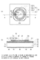
図1は、本発明の第1の実施形態にかかる発光装置の模式図である。すなわち、図1(a)は平面図、図1(b)はA−A線に沿った断面図である。
GaPなどからなる透光性基板10の上に、第1のクラッド層14、発光層16、第2のクラッド層18、電流拡散層20、などからなる半導体積層体が設けられている。
Hereinafter, embodiments of the present invention will be described with reference to the drawings.
FIG. 1 is a schematic diagram of a light emitting device according to a first embodiment of the present invention. 1A is a plan view, and FIG. 1B is a cross-sectional view taken along the line AA.
On the
電流拡散層20の上にはボンディング電極40と、細線電極42と、からなる上側電極43が設けられている。本図において、細線電極42は、ボンディング電極40と距離L1だけ離間し幅がW1である第1の細線電極42aと、第1の細線電極42aから距離L2だけ離間し幅がW2である第2の細線電極42bと、及び第2の細線電極42bから距離L3だけ離間し幅がW3である第3の細線電極42cと、ボンディング電極40との連結部42dと、を有している。ボンディング電極40は、連結部42dにより3つの細線電極42a、42b、及び42cと平面的に連結している。ボンディングにおけるワイヤのつぶれなどを考慮し、ボンディング電極40の直径Dは、例えば100μm近傍とすることができる。
On the
上側電極43に印加された電圧により、電流拡散層20を介して発光層16にキャリアが注入される。電流拡散層20は、電流を発光層16の結晶成長面に沿った横方向に広げて発光領域を拡大するが、上側電極43の直下から横方向に向かって離れるに従い電流が流れにくくなる。このために、細線電極42をボンディング電極40の周囲に一定距離L1、L2、L3だけ離間してそれぞれ配置し、発光層16のより広い横方向領域にキャリアが広がりやすくして光出力を高める。
Carriers are injected into the
この場合、ボンディング電極40及び細線電極42は発光層16から上方へ向かう放出光を遮る。このため、横方向へ電流を拡散をしつつ上方へ放出光G1を出射可能なように、細線電極42の幅W1、W2、W3及び距離L1、L2、L3を適正に決定する。
In this case, the
他方、発光層16からGaP基板10へ向かう光は、透光性を有するGaP基板10内を透過しつつ下側電極45及び反射層46により反射されるか、または直接に、側方へ向かう放出光G2となる。
On the other hand, the light traveling from the
GaP及びInGaAlP系材料においては、キャリア濃度を高めると結晶性低下などを生じ光吸収が増加する。本実施形態では、上側電極43の非形成領域であり、電流密度が低くなる電流拡散層20の領域の一部を除去して凹部20cを形成し、光吸収を低減し高輝度とする。凹部20cは、電流拡散層20を貫通していない。つまり、凹部20cの深さは、電流拡散層20の厚みよりも小さい。また、細線電極42にはワイヤボンディングを行う必要がないので、横方向へ電流を拡散可能である範囲内において、その幅W1、W2、W3を狭くし光取り出し効率を高める。なお、電流拡散層20の構造及び作用に関しては、のちに説明する。
In GaP and InGaAlP-based materials, when the carrier concentration is increased, crystallinity is lowered and light absorption is increased. In the present embodiment, the
図2は、本実施形態にかかる発光装置の製造方法を説明するフローチャートである。
また、図3は、エピタキシャルウェーハの模式断面図である。
透光性を有しn型であるGaP基板10と界面11において接着し、n型InGaAlPなどを含む接着層12(厚さ0.4μm、キャリア濃度4×1017cm−3)上に、上部成長層25が積層されている。
FIG. 2 is a flowchart illustrating a method for manufacturing the light emitting device according to the present embodiment.
FIG. 3 is a schematic cross-sectional view of an epitaxial wafer.
Adhering to the
上部成長層25としては、n型InAlPからなるクラッド層14(厚さ0.6μm、キャリア濃度4×1017cm−3)、In0.5(GaxAl1−x)0.5P(0≦x≦1)からなる発光層16、p型InAlPからなるクラッド層18(厚さ0.6μm、キャリア濃度4×1017cm−3)、p型Iny(Ga0.3Al0.7)1−yP(0≦y≦1)からなる電流拡散層20(厚さ1.5μm、キャリア濃度1.5×1018cm−3)、p型InGaAlPからなる中間層22(厚さ0.1μm、キャリア濃度3×1018cm−3)、及びp型GaAsからなるコンタクト層24、をこの順序で積層する(S100)。なお、電流拡散層20を、例えば第1の層20b(厚さ0.2μm、キャリア濃度4×1017cm−3)と、第2の層20a(厚さ1.3μm、キャリア濃度1.5×1018cm−3)と、の2つの層とすることもできる。
As the
また、発光層16を、例えば多重量子井戸構造とすると、動作電流の低減及び可視〜赤外光波長範囲において発光波長の制御が容易となる。この上部成長層25は、MOCVD(Metal Organic Chemical Vapor Deposition )法及びMBE(Molecular Beam Epitaxy)法などを用いて結晶成長可能である。
Further, when the
GaP基板10のマウント面側に、スパッタ法または蒸着法などを用いてAuGeなどからなる下側電極45及び反射層46を形成する(S102)。この場合、下側電極45の被覆率を30%などとし、反射層46を誘電体多層膜または金属などを用いて形成すると、下面において光吸収を低減し高輝度とすることが容易となる。
A
さらに、上部成長層25の上に、リフトオフ法などを用いてAnZnなどからなる上側電極43を形成する(S104)。のちに電流拡散層20の表面に凹部20cを形成する工程において、細線電極42の直下がオーバーエッチングとなると、細線電極42と発光層16との間に高い直列抵抗を生じること、または細線電極42が消失すること、などにより発光層16へのキャリア注入が不十分となりやすい。細線電極42の幅W1、W2、及びW3を3μm以上、より好ましくは5μm以上とすると、確実にキャリアを発光層16へ注入できる。 なお、GaP基板10をn型とする場合、上側電極43はp型電極、下側電極45はn型電極となる。
Further, the
続いて、上側電極43と電流拡散層20との間に設けられているコンタクト層24及び中間層22のうち、上側電極43の非形成領域をエッチングにより除去する(S106)。コンタクト層24を構成するGaAsは、可視光を吸収し光出力を低下させるので除去することが好ましい。
Subsequently, in the
このあと、シンター工程などを行いコンタクト層24と上側電極43との間、及びGaP基板10と下側電極45との間、をそれぞれオーミック接触とする。続いて、電流拡散層20のうち、上側電極43の非形成領域の一部にエッチング法を用いて凹部20cを形成する。この場合、上側電極43をマスクとして塩酸系、燐酸系、及び硫酸系などのエッチング溶液を用いて電流が拡散されにくい領域に凹部20cを形成する(S108)。なお、上側電極43をマスクとせずに、凹部20cをパターニングにより形成することもできる。
Thereafter, a sintering process or the like is performed to make ohmic contact between the
ウェーハ状態において凹部20cに樹脂などの透光性を有する誘電体を充填するかを判断し(S110)、充填しない場合、素子分離工程(S116)へと進む。
In the wafer state, it is determined whether or not the
他方、樹脂などを凹部20c内に充填する場合、スピンコート法などを用いて、ウェーハ表面に均一に樹脂を塗布する(S112)。必要に応じて樹脂硬化を行い、CDE(Chemical Dry Etching)法などのドライエッチング法を用いてボンディング電極40の表面を露出させる(S114)。なお、誘電体としてAlN(窒化アルミニウム)などを用いる場合、スパッタ法やCVD(Chemical Vapor Deposition)法を用いることができる。
On the other hand, when filling the
このあと素子分離を行い(S116)、実装部材にチップ接着及びワイヤボンディングなどを行い発光装置を組み立てる(S118)。この場合、チップを覆うように封止樹脂を形成すると、チップの保護が容易となり、且つ光取り出し効率を高めることが容易となる。ウェーハ状態で誘電体を形成しない場合、素子分離ののちの組立工程において、凹部20cに封止樹脂を充填する。この様にして、光吸収が低減され且つ光取り出し効率が改善され、高輝度を得ることが可能な発光装置の量産性に富む製造方法が提供される。
Thereafter, element isolation is performed (S116), and chip mounting and wire bonding are performed on the mounting member to assemble the light emitting device (S118). In this case, if the sealing resin is formed so as to cover the chip, the chip can be easily protected and the light extraction efficiency can be easily increased. When the dielectric is not formed in the wafer state, the
また、本実施形態にかかる製造方法では、凹部20cの深さを発光層16に到達させる必要が無く、凹部20cの形成プロセスが容易である。発光層16を露出させると、その形成プロセスにより発光層16の内部または表面に、結晶欠陥を生じ輝度低下または通電劣化などを生じることがある。発光層16の発光領域が露出していない本実施形態では、結晶欠陥の発生が抑制され、より高い信頼性を確保するのが容易である。
Further, in the manufacturing method according to the present embodiment, it is not necessary to make the depth of the
次に、凹部20cの構造及びその作用について説明する。
図4は、チップ表面近傍におけるNFP(Near Field Pattern:近視野像)を説明する図である。すなわち、図4(a)は第1の実施形態、図4(b)は比較例をそれぞれ表す。
図4(a)において、ボンディング電極40と細線電極42aとの距離L1、細線電極42と細線電極42bとの距離L2、及び細線電極42bと細線電極42cとの間の距離L3、はそれぞれ略20μmとしているが、もちろんこれに限定されるものではない。なお、本図では、図1(a)のA−A線に沿った径方向位置に沿ったNFPの相対発光強度を表している。
Next, the structure and operation of the
FIG. 4 is a diagram for explaining an NFP (Near Field Pattern) near the chip surface. 4A shows the first embodiment, and FIG. 4B shows a comparative example.
In FIG. 4A, the distance L1 between the
ボンディング電極40及び細線電極42からチップの縦方向に流れる電流は、電流拡散層20により横方向に広がり、破線で表す方向に沿ってキャリアJが発光層16に注入される。このため、上側電極43の直下近傍よりも広がった発光層16内の発光領域Kから放出光が出射可能となる。
Current flowing in the vertical direction of the chip from the
例えば図1(a)のA−A線に沿った断面において、エッチングにより形成された凹部20cを通過した放出光により上側電極43の端部近傍でNFPの相対発光強度が極大となり、上方から見て上側電極43に挟まれた中間近傍で極小となる。なお、図4(a)において、チップ上面には屈折率n1の封止樹脂52が充填されているものとする。封止樹脂52としては、エポキシ及びシリコーンなどがあり、これらの屈折率n1は、例えば1.4〜1.5の範囲内にある。
For example, in the cross section taken along the line AA in FIG. 1A, the relative light emission intensity of NFP is maximized near the end of the
他方、図4(b)は、比較例にかかる発光装置を表す図である。比較例において、電流拡散層120は、凹部を有しておらず、その上部は屈折率n1が1.4の封止樹脂で覆われているものとする。電流拡散層120のキャリア濃度を1.5×1018cm−3,その厚さを1.5μmとすると、ボンディング電極140と細線電極142aとの間、及び細線電極142aと142bとの間、のそれぞれの領域120aは、電流が十分には拡散しない上に、高濃度による結晶性の低下などのため光吸収が大きい。すなわち、光取り出し効率を低下させている。この結果、領域120aの中央部近傍においてNFPの相対発光強度はゼロ近傍まで低下することがある。
On the other hand, FIG.4 (b) is a figure showing the light-emitting device concerning a comparative example. In the comparative example, it is assumed that the current spreading
これに対して、図4(a)に表す本実施形態のNFPの相対発光強度は、上側電極43の中間近傍においてもその低下量が少なく、高輝度を保つことが容易である。
On the other hand, the relative light emission intensity of the NFP of this embodiment shown in FIG. 4A is small even in the vicinity of the middle of the
なお、図4(a)において、凹部20cの深さは電流拡散層20の厚さよりも小さいが、凹部20cが電流拡散層20を略貫通し、クラッド層18が露出していてもよい。また、電流拡散層20が、キャリア濃度が4×1017cm−3且つ厚さが0.2μmの第1の層20bと、その上に設けられたキャリア濃度が1.5×1018cm−3且つ厚さが1.3μmの第2の層20aと、を有する構造とすることができる。この場合、光吸収が大きい第2の層20aは除去されるので高い光出力を保ちつつ、残っている第1の層20bにより電流を横方向へ広げることが容易となる。
In FIG. 4A, the depth of the
なお、エッチング溶液を適正に選択し、凹部20cの側壁を図4(a)のように傾斜させると、電流の拡散が容易となり、側壁近傍において上方への光の取り出し効率をより高めることが容易となる。
If the etching solution is appropriately selected and the side wall of the
図5は、第2の実施形態にかかる発光装置を表す図である。
本実施形態では、凹部20c内に電流拡散層20の屈折率n3と、封止樹脂52の屈折率n1と、の間の屈折率n2(ただし、n3>n2≧n1)を有する透光性誘電体50を充填する。
FIG. 5 is a diagram illustrating a light emitting device according to the second embodiment.
In this embodiment, the refractive index n 3 of the
例えば電流拡散層20の屈折率n3を3.2とし、発光素子チップの表面を覆う封止樹脂52の屈折率n1を1.4とすると、チップ内部から封止樹脂52へ直接出射する場合の臨界角θC1は略26°となる。また、透光性誘電体50の屈折率n2を1.74とすると、電流拡散層20と透光性誘電体50との界面の臨界角θc3は略34°であり、透光性誘電体50と封止樹脂52との界面の臨界角θC2は略53°となる。
For example, when the refractive index n 3 of the
他方、図4(b)の比較例では、臨界角θC1は略26°であるので、光取り出し可能な放出光の角度範囲が狭く、電流拡散層120と封止樹脂との界面で全反射する割合が増える。界面で反射された光は、チップ内部で多重反射を繰り返し、ついには熱損失となるので光取り出し効率を低下させる。
On the other hand, in the comparative example of FIG. 4B, since the critical angle θ C1 is approximately 26 °, the angle range of emitted light that can be extracted is narrow, and total reflection is performed at the interface between the
これに対して、本実施形態では、屈折率が電流拡散層20と封止樹脂52との中間の範囲にある透光性誘電体50を介して放出光を外部に取り出すことにより、それぞれの界面での全反射を低減し光取り出し効率を高め、鎖線で表すNFPの相対発光強度が実線で表す第1の実施形態の相対発光強度よりも高くできる。このために、高輝度とすることがより容易となる。
On the other hand, in the present embodiment, the emitted light is extracted to the outside through the
なお、透光性の誘電体50として、例えばチオウレタン系樹脂を用いることができる。この屈折率は、例えば1.7〜1.74である。なお、透光性を有する金属酸化物などの微粒子を透光性樹脂に分散配置するとより高い屈折率とでき、より高輝度とすることが容易となる。
For example, a thiourethane resin can be used as the
第2の実施形態は、透光性誘電体50をポリイミド樹脂などとし、その屈折率n2と、封止樹脂52の屈折率n1と、が近い場合も含むものとする。さらに透光性の誘電体50と封止樹脂52とが同一材料であってもよく、例えば、封止樹脂52が凹部20c内を充填していてもよい。
The second embodiment includes a case where the
以上の実施形態において、GaP基板10の導電型をn型及び電流拡散層20の導電型をp型としたが、本発明はこれに限定されず、GaP基板10の導電型をp型及び電流拡散層の導電型をn型としてもよい。
In the above embodiment, the conductivity type of the
なお、本明細書において、InGaAlP系とは、Inx(GayAl1−y)1−xP(ただし、0≦x≦1、0≦y≦1)なる組成式で表される材料であり、p型不純物やn型不純物が添加されたものも含むものとする。 Note that in this specification, the InGaAlP-based material is a material represented by a composition formula of In x (Ga y Al 1-y ) 1-x P (where 0 ≦ x ≦ 1, 0 ≦ y ≦ 1). Yes, including those to which p-type impurities or n-type impurities are added.
しかし、本発明はこれに限定されず、例えばInz(GawAl1−w)1−zN(ただし、0≦z≦1、0≦w≦1)なる組成式で表される材料であり、p型不純物やn型不純物が添加されたものも含むものとする。この場合、樹脂に蛍光体を分散配置すると、蛍光体による波長変換光と発光層16からの放出光との混合光を高輝度とすることができる。
However, the present invention is not limited to this, and is, for example, a material represented by a composition formula of In z (Ga w Al 1-w ) 1-z N (where 0 ≦ z ≦ 1, 0 ≦ w ≦ 1). Yes, including those to which p-type impurities or n-type impurities are added. In this case, when the phosphors are dispersedly arranged in the resin, the mixed light of the wavelength-converted light by the phosphor and the light emitted from the
以上、図面を参照しつつ、本発明の実施の形態について説明した。しかしながら本発明は、これらの実施形態に限定されない。本発明を構成する基板、発光層、電流拡散層、凹部、ボンディング電極、細線電極、下側電極、封止樹脂、透光性誘電体などの材質、サイズ、形状、配置などに関して当業者が設計変更を行ったものであっても、本発明の主旨を逸脱しない限り本発明の範囲に包含される。 The embodiments of the present invention have been described above with reference to the drawings. However, the present invention is not limited to these embodiments. Designed by those skilled in the art regarding the material, size, shape, arrangement, etc. of the substrate, light emitting layer, current spreading layer, recess, bonding electrode, fine wire electrode, lower electrode, sealing resin, translucent dielectric, etc. constituting the present invention Even if it changes, unless it deviates from the main point of this invention, it is included in the scope of the present invention.
10 GaP基板、16 発光層、20 電流拡散層、20c 凹部、40 ボンディング電極、42 細線電極、43 上側電極、50 透光性誘電体、52 封止樹脂、G1、G2 放出光 10 GaP substrate, 16 light emitting layer, 20 current diffusion layer, 20c recess, 40 bonding electrode, 42 fine wire electrode, 43 upper electrode, 50 translucent dielectric, 52 sealing resin, G1, G2 emission light
Claims (4)
上側電極と、
前記発光層と前記上側電極との間に設けられ、前記発光層の側の第1の層と、前記第1の層のキャリア濃度よりも高いキャリア濃度を有し前記上側電極の側に設けられた第2の層と、を有する電流拡散層であって、前記上側電極の非形成領域に設けられ前記発光層のの側に向かうに従って幅が狭くなる凹部を有し、前記第2の層上に前記上側電極が設けられ、前記第2の層の側面は前記凹部の側面の少なくとも一部である、電流拡散層と、
前記発光層に対して前記電流拡散層とは反対の面の側に設けられた反射層と、
を備えたことを特徴とする発光装置。 A light emitting layer;
An upper electrode;
Provided between the light emitting layer and the upper electrode, and provided on the upper electrode side having a carrier concentration higher than that of the first layer on the light emitting layer side and the carrier concentration of the first layer. and a second layer, a current diffusion layer having the provided non-formation region of the upper electrode have a recess width is reduced toward the side of the light-emitting layer, the second layer on the The upper electrode is provided, and the side surface of the second layer is at least a part of the side surface of the recess, and a current spreading layer;
A reflective layer provided on the side of the light emitting layer opposite to the current diffusion layer;
A light-emitting device comprising:
Priority Applications (1)
| Application Number | Priority Date | Filing Date | Title |
|---|---|---|---|
| JP2012263647A JP5572202B2 (en) | 2012-11-30 | 2012-11-30 | Light emitting device |
Applications Claiming Priority (1)
| Application Number | Priority Date | Filing Date | Title |
|---|---|---|---|
| JP2012263647A JP5572202B2 (en) | 2012-11-30 | 2012-11-30 | Light emitting device |
Related Parent Applications (1)
| Application Number | Title | Priority Date | Filing Date |
|---|---|---|---|
| JP2008137945A Division JP5150367B2 (en) | 2008-05-27 | 2008-05-27 | Light emitting device and manufacturing method thereof |
Publications (2)
| Publication Number | Publication Date |
|---|---|
| JP2013048298A JP2013048298A (en) | 2013-03-07 |
| JP5572202B2 true JP5572202B2 (en) | 2014-08-13 |
Family
ID=48011075
Family Applications (1)
| Application Number | Title | Priority Date | Filing Date |
|---|---|---|---|
| JP2012263647A Active JP5572202B2 (en) | 2012-11-30 | 2012-11-30 | Light emitting device |
Country Status (1)
| Country | Link |
|---|---|
| JP (1) | JP5572202B2 (en) |
Family Cites Families (6)
| Publication number | Priority date | Publication date | Assignee | Title |
|---|---|---|---|---|
| JP2546097Y2 (en) * | 1991-12-26 | 1997-08-27 | 関西日本電気株式会社 | Light emitting diode |
| JP3122324B2 (en) * | 1995-02-20 | 2001-01-09 | 三菱電線工業株式会社 | Semiconductor light emitting device |
| US6291839B1 (en) * | 1998-09-11 | 2001-09-18 | Lulileds Lighting, U.S. Llc | Light emitting device having a finely-patterned reflective contact |
| JP3576963B2 (en) * | 2000-11-24 | 2004-10-13 | 三菱電線工業株式会社 | Semiconductor light emitting device |
| JP4332440B2 (en) * | 2004-02-04 | 2009-09-16 | シャープ株式会社 | Light emitting diode manufacturing method, light emitting diode |
| JP4371029B2 (en) * | 2004-09-29 | 2009-11-25 | サンケン電気株式会社 | Semiconductor light emitting device and manufacturing method thereof |
-
2012
- 2012-11-30 JP JP2012263647A patent/JP5572202B2/en active Active
Also Published As
| Publication number | Publication date |
|---|---|
| JP2013048298A (en) | 2013-03-07 |
Similar Documents
| Publication | Publication Date | Title |
|---|---|---|
| KR101014102B1 (en) | Semiconductor light emitting device and fabrication method thereof | |
| KR101729263B1 (en) | Light emitting device, method for fabricating the light emitting device and light emitting device package | |
| KR101017394B1 (en) | Light emitting device and method of fabricating the same | |
| KR100714638B1 (en) | Facet extraction type led and method for manufacturing the same | |
| US9029875B2 (en) | Light emitting device and method for manufacturing the same | |
| KR101154709B1 (en) | Light emitting device, method for fabricating the light emitting device, light emitting device package and lighting system | |
| JP5150367B2 (en) | Light emitting device and manufacturing method thereof | |
| JP5531575B2 (en) | Group III nitride compound semiconductor light emitting device | |
| JP2012256811A (en) | Semiconductor light-emitting element | |
| JP2010087292A (en) | Light emitting element | |
| CN105932134A (en) | Lighting Emitting Device Package And Lighting Apparatus Including The Same | |
| US20080265272A1 (en) | Light Emitting Device Having Zener Diode Therein And Method Of Fabricating The Same | |
| KR100748247B1 (en) | Nitride semiconductor light emitting diode and method of manufacturing the same | |
| JP5075786B2 (en) | Light emitting device and manufacturing method thereof | |
| JP5933075B2 (en) | Semiconductor light emitting device | |
| JP2012009864A (en) | Semiconductor light-emitting element | |
| JP6684541B2 (en) | Light emitting element | |
| JP2014165337A (en) | Light-emitting element, light-emitting element package, and method of manufacturing light-emitting element | |
| KR20070097619A (en) | Light emitting device having zenor diode therein and method of fabricating the same | |
| KR20110132161A (en) | Semiconductor light emitting diode and method of manufacturing thereof | |
| KR101221643B1 (en) | Flip chip Light-emitting device and Method of manufacturing the same | |
| JP4501234B2 (en) | Nitride semiconductor device | |
| JP5572202B2 (en) | Light emitting device | |
| KR101916369B1 (en) | Light emitting diode | |
| KR100836132B1 (en) | Nitride semiconductor light emitting diode |
Legal Events
| Date | Code | Title | Description |
|---|---|---|---|
| A621 | Written request for application examination |
Free format text: JAPANESE INTERMEDIATE CODE: A621 Effective date: 20121130 |
|
| A977 | Report on retrieval |
Free format text: JAPANESE INTERMEDIATE CODE: A971007 Effective date: 20130814 |
|
| A131 | Notification of reasons for refusal |
Free format text: JAPANESE INTERMEDIATE CODE: A131 Effective date: 20130826 |
|
| A521 | Written amendment |
Free format text: JAPANESE INTERMEDIATE CODE: A523 Effective date: 20131015 |
|
| TRDD | Decision of grant or rejection written | ||
| A01 | Written decision to grant a patent or to grant a registration (utility model) |
Free format text: JAPANESE INTERMEDIATE CODE: A01 Effective date: 20140529 |
|
| A61 | First payment of annual fees (during grant procedure) |
Free format text: JAPANESE INTERMEDIATE CODE: A61 Effective date: 20140627 |
|
| R150 | Certificate of patent or registration of utility model |
Ref document number: 5572202 Country of ref document: JP Free format text: JAPANESE INTERMEDIATE CODE: R150 |
|
| S111 | Request for change of ownership or part of ownership |
Free format text: JAPANESE INTERMEDIATE CODE: R313115 |
|
| R350 | Written notification of registration of transfer |
Free format text: JAPANESE INTERMEDIATE CODE: R350 |
|
| S111 | Request for change of ownership or part of ownership |
Free format text: JAPANESE INTERMEDIATE CODE: R313115 |
|
| R350 | Written notification of registration of transfer |
Free format text: JAPANESE INTERMEDIATE CODE: R350 |