JP5539406B2 - リソグラフィマシン及び基板処理構成体 - Google Patents
リソグラフィマシン及び基板処理構成体 Download PDFInfo
- Publication number
- JP5539406B2 JP5539406B2 JP2011550596A JP2011550596A JP5539406B2 JP 5539406 B2 JP5539406 B2 JP 5539406B2 JP 2011550596 A JP2011550596 A JP 2011550596A JP 2011550596 A JP2011550596 A JP 2011550596A JP 5539406 B2 JP5539406 B2 JP 5539406B2
- Authority
- JP
- Japan
- Prior art keywords
- lithographic apparatus
- chamber
- door
- vacuum
- vacuum chamber
- Prior art date
- Legal status (The legal status is an assumption and is not a legal conclusion. Google has not performed a legal analysis and makes no representation as to the accuracy of the status listed.)
- Expired - Fee Related
Links
Images


Classifications
-
- H—ELECTRICITY
- H01—ELECTRIC ELEMENTS
- H01J—ELECTRIC DISCHARGE TUBES OR DISCHARGE LAMPS
- H01J37/00—Discharge tubes with provision for introducing objects or material to be exposed to the discharge, e.g. for the purpose of examination or processing thereof
- H01J37/02—Details
- H01J37/16—Vessels; Containers
-
- B—PERFORMING OPERATIONS; TRANSPORTING
- B82—NANOTECHNOLOGY
- B82Y—SPECIFIC USES OR APPLICATIONS OF NANOSTRUCTURES; MEASUREMENT OR ANALYSIS OF NANOSTRUCTURES; MANUFACTURE OR TREATMENT OF NANOSTRUCTURES
- B82Y10/00—Nanotechnology for information processing, storage or transmission, e.g. quantum computing or single electron logic
-
- B—PERFORMING OPERATIONS; TRANSPORTING
- B82—NANOTECHNOLOGY
- B82Y—SPECIFIC USES OR APPLICATIONS OF NANOSTRUCTURES; MEASUREMENT OR ANALYSIS OF NANOSTRUCTURES; MANUFACTURE OR TREATMENT OF NANOSTRUCTURES
- B82Y40/00—Manufacture or treatment of nanostructures
-
- H—ELECTRICITY
- H01—ELECTRIC ELEMENTS
- H01J—ELECTRIC DISCHARGE TUBES OR DISCHARGE LAMPS
- H01J37/00—Discharge tubes with provision for introducing objects or material to be exposed to the discharge, e.g. for the purpose of examination or processing thereof
- H01J37/02—Details
- H01J37/18—Vacuum locks ; Means for obtaining or maintaining the desired pressure within the vessel
-
- H—ELECTRICITY
- H01—ELECTRIC ELEMENTS
- H01J—ELECTRIC DISCHARGE TUBES OR DISCHARGE LAMPS
- H01J37/00—Discharge tubes with provision for introducing objects or material to be exposed to the discharge, e.g. for the purpose of examination or processing thereof
- H01J37/30—Electron-beam or ion-beam tubes for localised treatment of objects
- H01J37/317—Electron-beam or ion-beam tubes for localised treatment of objects for changing properties of the objects or for applying thin layers thereon, e.g. for ion implantation
- H01J37/3174—Particle-beam lithography, e.g. electron beam lithography
- H01J37/3177—Multi-beam, e.g. fly's eye, comb probe
-
- H—ELECTRICITY
- H01—ELECTRIC ELEMENTS
- H01J—ELECTRIC DISCHARGE TUBES OR DISCHARGE LAMPS
- H01J37/00—Discharge tubes with provision for introducing objects or material to be exposed to the discharge, e.g. for the purpose of examination or processing thereof
- H01J37/32—Gas-filled discharge tubes
-
- H—ELECTRICITY
- H01—ELECTRIC ELEMENTS
- H01L—SEMICONDUCTOR DEVICES NOT COVERED BY CLASS H10
- H01L21/00—Processes or apparatus adapted for the manufacture or treatment of semiconductor or solid state devices or of parts thereof
- H01L21/67—Apparatus specially adapted for handling semiconductor or electric solid state devices during manufacture or treatment thereof; Apparatus specially adapted for handling wafers during manufacture or treatment of semiconductor or electric solid state devices or components ; Apparatus not specifically provided for elsewhere
- H01L21/67005—Apparatus not specifically provided for elsewhere
- H01L21/67011—Apparatus for manufacture or treatment
- H01L21/67155—Apparatus for manufacturing or treating in a plurality of work-stations
- H01L21/67161—Apparatus for manufacturing or treating in a plurality of work-stations characterized by the layout of the process chambers
- H01L21/67173—Apparatus for manufacturing or treating in a plurality of work-stations characterized by the layout of the process chambers in-line arrangement
-
- H—ELECTRICITY
- H01—ELECTRIC ELEMENTS
- H01L—SEMICONDUCTOR DEVICES NOT COVERED BY CLASS H10
- H01L21/00—Processes or apparatus adapted for the manufacture or treatment of semiconductor or solid state devices or of parts thereof
- H01L21/67—Apparatus specially adapted for handling semiconductor or electric solid state devices during manufacture or treatment thereof; Apparatus specially adapted for handling wafers during manufacture or treatment of semiconductor or electric solid state devices or components ; Apparatus not specifically provided for elsewhere
- H01L21/67005—Apparatus not specifically provided for elsewhere
- H01L21/67011—Apparatus for manufacture or treatment
- H01L21/67155—Apparatus for manufacturing or treating in a plurality of work-stations
- H01L21/67161—Apparatus for manufacturing or treating in a plurality of work-stations characterized by the layout of the process chambers
- H01L21/67178—Apparatus for manufacturing or treating in a plurality of work-stations characterized by the layout of the process chambers vertical arrangement
-
- H—ELECTRICITY
- H01—ELECTRIC ELEMENTS
- H01L—SEMICONDUCTOR DEVICES NOT COVERED BY CLASS H10
- H01L21/00—Processes or apparatus adapted for the manufacture or treatment of semiconductor or solid state devices or of parts thereof
- H01L21/67—Apparatus specially adapted for handling semiconductor or electric solid state devices during manufacture or treatment thereof; Apparatus specially adapted for handling wafers during manufacture or treatment of semiconductor or electric solid state devices or components ; Apparatus not specifically provided for elsewhere
- H01L21/67005—Apparatus not specifically provided for elsewhere
- H01L21/67011—Apparatus for manufacture or treatment
- H01L21/67155—Apparatus for manufacturing or treating in a plurality of work-stations
- H01L21/67207—Apparatus for manufacturing or treating in a plurality of work-stations comprising a chamber adapted to a particular process
- H01L21/67225—Apparatus for manufacturing or treating in a plurality of work-stations comprising a chamber adapted to a particular process comprising at least one lithography chamber
Landscapes
- Engineering & Computer Science (AREA)
- Chemical & Material Sciences (AREA)
- Physics & Mathematics (AREA)
- Analytical Chemistry (AREA)
- Condensed Matter Physics & Semiconductors (AREA)
- Manufacturing & Machinery (AREA)
- General Physics & Mathematics (AREA)
- Nanotechnology (AREA)
- Microelectronics & Electronic Packaging (AREA)
- Computer Hardware Design (AREA)
- Power Engineering (AREA)
- Crystallography & Structural Chemistry (AREA)
- Theoretical Computer Science (AREA)
- Mathematical Physics (AREA)
- Plasma & Fusion (AREA)
- Electron Beam Exposure (AREA)
- Exposure And Positioning Against Photoresist Photosensitive Materials (AREA)
Description
以下に、本発明の出願当初の特許請求の範囲を付記する。
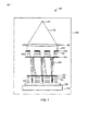
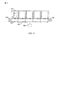
[1]複数の荷電粒子リソグラフィ装置を具備する構成体であって、各荷電粒子リソグラフィ装置は、真空チャンバ(400)を有し、構成体は、前記複数のリソグラフィ装置にウェーハを運搬するための共通のロボット(305)と、夫々の真空チャンバ(400)の前面に配置された、各荷電粒子リソグラフィ装置のためのウェーハロードユニット(303)とをさらに具備し、前記複数のリソグラフィ装置は、これらリソグラフィ装置の前面が、各装置にウェーハを運搬するための前記共通のロボット(305)の通路を収容している通路(310)に面している状態で、列をなして配置され、各リソグラフィ装置の後面は、アクセス通路(306)に面し、各真空チャンバの後壁には、夫々のリソグラフィ装置へのアクセスのためのアクセスドアが設けられている構成体。
[2]前記複数のリソグラフィ装置は、中央の共通の通路を有するようにして2列で配置されている[1]の構成体。
[3]前記2列のリソグラフィ装置は、これらの間の前記中央の通路に対して互いに対向して配置されている[2]の構成体。
[4]前記2列のリソグラフィ装置は、前記中央の共通の通路に面している両方の列に垂直に積み重ねられている[2]の構成体。
[5]前記複数のリソグラフィ装置は、中央の共通の通路を有するようにして複数の列で配置され、前記列のリソグラフィ装置の少なくとも2つが、これらの間の前記中央の共通の通路に対して互いに対向して配置され、前記列のリソグラフィ装置の少なくとも2つが、前記中央の共通の通路に面している両方の列に垂直に積み重ねられている[1]の構成体。
[6]各リソグラフィ装置には、その前壁にロードロックユニット(303)が設けられている[1]ないし[5]のいずれか1の構成体。
[7]各荷電粒子リソグラフィ装置のためのステージアクチュエータ(304)が、夫々のリソグラフィ装置の前面に配置されている[1]ないし[6]のいずれか1の構成体。
[8]各荷電粒子リソグラフィ装置に対して、夫々のチャンバ(400)の内部でステージを動かすために、駆動部材又はロッドを有するステージアクチュエータ(304)が設けられている[1]ないし[7]のいずれか1の構成体。
[9]前記ロードロックユニット(303)は、夫々のリソグラフィ装置の前記ステージアクチュエータ(304)の上方に配置されている[7]又は[8]の構成体。
[10]前記共通のロボットは、少なくとも2つのロボットユニットを有する[1]ないし[9]のいずれか1の構成体。
[11]前記構成体は、ロボット保管ユニット(307)をさらに有する[1]ないし[10]のいずれか1の構成体。
[12]前記保管ユニットは、前記通路に隣接しているリソグラフィ装置の列の一端に配置されている[11]の構成体。
[13]列をなしている前記リソグラフィ装置の少なくとも1つは、複数の層で垂直に積み重ねられている[1]ないし[12]のいずれか1の構成体。
[14]各リソグラフィ装置には、床からの個別の支持体が設けられている[13]の構成体。
[15]リソグラフィ装置の各層には、床への個々の支持体が設けられている[13]の構成体。
[16]各々が真空チャンバ(400)中に配置された複数のリソグラフィ処理ユニットを具備する荷電粒子リソグラフィマシンであって、このマシンは、さらに、前記複数の処理ユニットにウェーハを運搬するための共通のロボット(305)と、夫々の真空チャンバ(400)の前面に配置された、各処理ユニットのためのウェーハロードユニット(303)とを具備し、前記複数の処理ユニットは、これらリソグラフィ装置の前面が、各処理ユニットにウェーハを運搬するための前記共通のロボット(305)の通路を収容している通路(310)に面している状態で、列をなして配置され、各処理ユニットの後面は、アクセス通路(306)に面し、各真空チャンバの後壁には、夫々の処理ユニットへのアクセスのためのアクセスドアが設けられているマシン。
[17]前記複数の処理ユニットは、中央の共通の通路を有するようにして2列で設けられている[16]のマシン。
[18]前記2列の処理ユニットは、これらの間に前記中央の共通の通路に対して互いに対向して配置されている[17]のマシン。
[19]前記2列の処理ユニットは、前記中央の共通の通路に面している両方の列に垂直に積み重ねられている[17]のマシン。
Claims (14)
- 複数の荷電粒子リソグラフィ装置を具備する構成体であって、
各荷電粒子リソグラフィ装置は、真空チャンバ(400)を有し、
構成体は、
前記複数のリソグラフィ装置の各荷電粒子リソグラフィ装置にウェーハを運搬するための共通のロボット(305)と、
夫々の真空チャンバ(400)の前面に配置された、各荷電粒子リソグラフィ装置のためのウェーハロードユニット(303)とをさらに具備し、
前記複数のリソグラフィ装置は、これらリソグラフィ装置の前面が、前記共通のロボット(305)の通路を収容している領域に面している状態で、列をなして配置され、
各リソグラフィ装置は、夫々のリソグラフィ装置へのアクセスのためのドア(402)が設けられ、
前記ドア(402)は、前記夫々のリソグラフィ装置の前記真空チャンバ(400)の完全な壁を形成する構成体。 - 前記複数のリソグラフィ装置は、2列で配置されている請求項1の構成体。
- 前記2列のリソグラフィ装置は、これらの間の中央の通路に対して互いに対向して配置されている請求項2の構成体。
- 前記2列のリソグラフィ装置は、垂直に積み重ねられている請求項2の構成体。
- 前記複数のリソグラフィ装置は、複数の列で配置され、
前記列のリソグラフィ装置の少なくとも2つが、これらの間の前記中央の共通の通路に対して互いに対向して配置され、
前記列のリソグラフィ装置の少なくとも2つが、中央の共通の通路に面している両方の列に垂直に積み重ねられている請求項1の構成体。 - 各リソグラフィ装置には、その前壁にロードロックユニット(303)が設けられている請求項1ないし5のいずれか1の構成体。
- 各荷電粒子リソグラフィ装置に対して、夫々のチャンバ(400)の内部でステージを動かすために、駆動部材又はロッドを有するステージアクチュエータ(304)が設けられている請求項1ないし6のいずれか1の構成体。
- 前記共通のロボットは、少なくとも2つのロボットユニットを有し、
各ロボットユニットは、前記共通のロボットに割り当てられた機能を果すように構成されている請求項1ないし7のいずれか1の構成体。 - 前記構成体は、ロボット保管ユニット(307)をさらに有する請求項1ないし8のいずれか1の構成体。
- 前記保管ユニットは、リソグラフィ装置の列の一端に配置されている請求項9の構成体。
- 列をなしている前記リソグラフィ装置の少なくとも1つは、複数の層で垂直に積み重ねられている請求項1ないし10のいずれか1の構成体。
- 各リソグラフィ装置には、床からの個別の支持体が設けられている請求項11の構成体。
- リソグラフィ装置の各層には、床への個々の支持体が設けられている請求項11の構成体。
- 前記複数の荷電粒子リソグラフィ装置と協働するための共通のウェーハロードシステムをさらに具備する請求項1ないし13のいずれか1の構成体。
Applications Claiming Priority (9)
| Application Number | Priority Date | Filing Date | Title |
|---|---|---|---|
| US15441109P | 2009-02-22 | 2009-02-22 | |
| US15441509P | 2009-02-22 | 2009-02-22 | |
| US61/154,415 | 2009-02-22 | ||
| US61/154,411 | 2009-02-22 | ||
| US28940709P | 2009-12-23 | 2009-12-23 | |
| US61/289,407 | 2009-12-23 | ||
| US30633310P | 2010-02-19 | 2010-02-19 | |
| US61/306,333 | 2010-02-19 | ||
| PCT/EP2010/052221 WO2010094804A1 (en) | 2009-02-22 | 2010-02-22 | Lithography machine and substrate handling arrangement |
Publications (3)
| Publication Number | Publication Date |
|---|---|
| JP2012518902A JP2012518902A (ja) | 2012-08-16 |
| JP2012518902A5 JP2012518902A5 (ja) | 2013-04-11 |
| JP5539406B2 true JP5539406B2 (ja) | 2014-07-02 |
Family
ID=42035939
Family Applications (1)
| Application Number | Title | Priority Date | Filing Date |
|---|---|---|---|
| JP2011550596A Expired - Fee Related JP5539406B2 (ja) | 2009-02-22 | 2010-02-22 | リソグラフィマシン及び基板処理構成体 |
Country Status (6)
| Country | Link |
|---|---|
| US (1) | US20110049393A1 (ja) |
| EP (1) | EP2399271B1 (ja) |
| JP (1) | JP5539406B2 (ja) |
| KR (1) | KR20110139699A (ja) |
| CN (1) | CN102414776A (ja) |
| WO (1) | WO2010094804A1 (ja) |
Families Citing this family (12)
| Publication number | Priority date | Publication date | Assignee | Title |
|---|---|---|---|---|
| JP5315100B2 (ja) * | 2009-03-18 | 2013-10-16 | 株式会社ニューフレアテクノロジー | 描画装置 |
| JP6158091B2 (ja) * | 2010-12-14 | 2017-07-05 | マッパー・リソグラフィー・アイピー・ビー.ブイ. | リソグラフィシステム及びこのようなリソグラフィシステムで基板を処理する方法 |
| JP6239583B2 (ja) * | 2012-03-20 | 2017-11-29 | マッパー・リソグラフィー・アイピー・ビー.ブイ. | ラジカルを輸送するための装置および方法 |
| US10586625B2 (en) | 2012-05-14 | 2020-03-10 | Asml Netherlands B.V. | Vacuum chamber arrangement for charged particle beam generator |
| KR101961914B1 (ko) * | 2012-05-14 | 2019-03-25 | 마퍼 리쏘그라피 아이피 비.브이. | 하전 입자 리소그래피 시스템 및 빔 생성기 |
| US11348756B2 (en) | 2012-05-14 | 2022-05-31 | Asml Netherlands B.V. | Aberration correction in charged particle system |
| NL2010624C2 (en) | 2013-04-08 | 2014-10-09 | Mapper Lithography Ip Bv | Cabinet for electronic equipment. |
| KR20160044005A (ko) * | 2013-08-16 | 2016-04-22 | 에이에스엠엘 네델란즈 비.브이. | 리소그래피 장치, 프로그램가능한 패터닝 디바이스 및 리소그래피 방법 |
| JP7422349B2 (ja) * | 2020-03-26 | 2024-01-26 | 国立研究開発法人物質・材料研究機構 | 走査型電子顕微鏡用電子銃チャンバー、これを含む電子銃及び走査電子顕微鏡 |
| KR20210132599A (ko) | 2020-04-24 | 2021-11-04 | 아이엠에스 나노패브릭케이션 게엠베하 | 대전 입자 소스 |
| EP4095882A1 (en) | 2021-05-25 | 2022-11-30 | IMS Nanofabrication GmbH | Pattern data processing for programmable direct-write apparatus |
| US12154756B2 (en) | 2021-08-12 | 2024-11-26 | Ims Nanofabrication Gmbh | Beam pattern device having beam absorber structure |
Family Cites Families (27)
| Publication number | Priority date | Publication date | Assignee | Title |
|---|---|---|---|---|
| US3157308A (en) | 1961-09-05 | 1964-11-17 | Clark Mfg Co J L | Canister type container and method of making the same |
| US3159408A (en) | 1961-10-05 | 1964-12-01 | Grace W R & Co | Chuck |
| US3365091A (en) * | 1964-10-30 | 1968-01-23 | Welding Research Inc | Vacuum chamber |
| US4524308A (en) | 1984-06-01 | 1985-06-18 | Sony Corporation | Circuits for accomplishing electron beam convergence in color cathode ray tubes |
| JPH04352410A (ja) * | 1991-05-30 | 1992-12-07 | Canon Inc | 半導体製造装置 |
| WO1994025880A1 (en) | 1993-04-30 | 1994-11-10 | Board Of Regents, The University Of Texas System | Megavoltage scanning imager and method for its use |
| JPH0936198A (ja) * | 1995-07-19 | 1997-02-07 | Hitachi Ltd | 真空処理装置およびそれを用いた半導体製造ライン |
| EP0766405A1 (en) | 1995-09-29 | 1997-04-02 | STMicroelectronics S.r.l. | Successive approximation register without redundancy |
| JPH09209150A (ja) * | 1996-02-06 | 1997-08-12 | Tokyo Electron Ltd | 真空チャンバ及びその製造方法 |
| JPH1054369A (ja) * | 1996-05-21 | 1998-02-24 | Ebara Corp | 真空ポンプの制御装置 |
| US6235634B1 (en) * | 1997-10-08 | 2001-05-22 | Applied Komatsu Technology, Inc. | Modular substrate processing system |
| JP3463855B2 (ja) * | 1997-12-18 | 2003-11-05 | 富士重工業株式会社 | 無段変速機の変速制御装置 |
| WO2000057456A1 (en) * | 1999-03-19 | 2000-09-28 | Electron Vision Corporation | Cluster tool for wafer processing having an electron beam exposure module |
| JP3019260B1 (ja) * | 1999-03-26 | 2000-03-13 | 株式会社日立製作所 | 電子ビ―ム描画装置 |
| JP2007147648A (ja) * | 2000-12-01 | 2007-06-14 | Ebara Corp | 欠陥検査方法及び基板検査装置 |
| US6855929B2 (en) * | 2000-12-01 | 2005-02-15 | Ebara Corporation | Apparatus for inspection with electron beam, method for operating same, and method for manufacturing semiconductor device using former |
| KR101060557B1 (ko) | 2002-10-25 | 2011-08-31 | 마퍼 리쏘그라피 아이피 비.브이. | 리소그라피 시스템 |
| CN101414536B (zh) | 2002-10-30 | 2011-01-19 | 迈普尔平版印刷Ip有限公司 | 电子束曝光系统 |
| EP1602121B1 (en) | 2003-03-10 | 2012-06-27 | Mapper Lithography Ip B.V. | Apparatus for generating a plurality of beamlets |
| ATE358885T1 (de) | 2003-05-28 | 2007-04-15 | Mapper Lithography Ip Bv | Beamlet-belichtungssystem mit geladenen teilchen |
| JP2005016255A (ja) * | 2003-06-27 | 2005-01-20 | Sumitomo Heavy Ind Ltd | 扉ロック装置、及び扉システム |
| JP2005032505A (ja) * | 2003-07-10 | 2005-02-03 | Nikon Corp | 磁気シールド構造及び露光装置 |
| JP4664293B2 (ja) | 2003-07-30 | 2011-04-06 | マッパー・リソグラフィー・アイピー・ビー.ブイ. | 変調器回路 |
| US7819079B2 (en) * | 2004-12-22 | 2010-10-26 | Applied Materials, Inc. | Cartesian cluster tool configuration for lithography type processes |
| US7709815B2 (en) | 2005-09-16 | 2010-05-04 | Mapper Lithography Ip B.V. | Lithography system and projection method |
| CN102986016B (zh) * | 2005-09-18 | 2015-11-25 | 弗雷德里克·A·弗里奇 | 用于在洁净空间中垂直定位基片处理设备的方法和装置 |
| US10168208B2 (en) | 2015-04-03 | 2019-01-01 | Hitachi High-Technologies Corporation | Light amount detection device, immune analyzing apparatus and charged particle beam apparatus that each use the light amount detection device |
-
2010
- 2010-02-22 JP JP2011550596A patent/JP5539406B2/ja not_active Expired - Fee Related
- 2010-02-22 KR KR1020117022202A patent/KR20110139699A/ko not_active Abandoned
- 2010-02-22 CN CN201080017870XA patent/CN102414776A/zh active Pending
- 2010-02-22 US US12/709,647 patent/US20110049393A1/en not_active Abandoned
- 2010-02-22 EP EP10704835A patent/EP2399271B1/en not_active Not-in-force
- 2010-02-22 WO PCT/EP2010/052221 patent/WO2010094804A1/en active Application Filing
Also Published As
| Publication number | Publication date |
|---|---|
| EP2399271A1 (en) | 2011-12-28 |
| KR20110139699A (ko) | 2011-12-29 |
| JP2012518902A (ja) | 2012-08-16 |
| US20110049393A1 (en) | 2011-03-03 |
| CN102414776A (zh) | 2012-04-11 |
| WO2010094804A1 (en) | 2010-08-26 |
| EP2399271B1 (en) | 2013-01-16 |
Similar Documents
| Publication | Publication Date | Title |
|---|---|---|
| JP5680557B2 (ja) | 荷電粒子リソグラフィ装置 | |
| JP5539406B2 (ja) | リソグラフィマシン及び基板処理構成体 | |
| JP5762981B2 (ja) | 荷電粒子リソグラフィ装置と、真空チャンバー内の真空を生成する方法 | |
| RU2579533C2 (ru) | Литографическая система и способ обработки подложек в такой литографической системе | |
| US9575418B2 (en) | Apparatus for transferring a substrate in a lithography system | |
| NL2010797A (en) | Charged particle lithography system and beam generator. | |
| TWI471891B (zh) | 帶電粒子微影機器及基板處理系統 | |
| US20230207252A1 (en) | Actuator arrangement and electron-optical column | |
| KR100344150B1 (ko) | 전자빔을 이용한 음극선관의 연속노광장치 | |
| JP2024544504A (ja) | 荷電粒子装置のためのプラットフォーム及び荷電粒子装置内のコンポーネント |
Legal Events
| Date | Code | Title | Description |
|---|---|---|---|
| A521 | Request for written amendment filed |
Free format text: JAPANESE INTERMEDIATE CODE: A523 Effective date: 20130222 |
|
| A621 | Written request for application examination |
Free format text: JAPANESE INTERMEDIATE CODE: A621 Effective date: 20130222 |
|
| TRDD | Decision of grant or rejection written | ||
| A01 | Written decision to grant a patent or to grant a registration (utility model) |
Free format text: JAPANESE INTERMEDIATE CODE: A01 Effective date: 20140401 |
|
| R150 | Certificate of patent or registration of utility model |
Ref document number: 5539406 Country of ref document: JP Free format text: JAPANESE INTERMEDIATE CODE: R150 |
|
| A61 | First payment of annual fees (during grant procedure) |
Free format text: JAPANESE INTERMEDIATE CODE: A61 Effective date: 20140430 |
|
| R250 | Receipt of annual fees |
Free format text: JAPANESE INTERMEDIATE CODE: R250 |
|
| R250 | Receipt of annual fees |
Free format text: JAPANESE INTERMEDIATE CODE: R250 |
|
| R250 | Receipt of annual fees |
Free format text: JAPANESE INTERMEDIATE CODE: R250 |
|
| S111 | Request for change of ownership or part of ownership |
Free format text: JAPANESE INTERMEDIATE CODE: R313113 |
|
| R350 | Written notification of registration of transfer |
Free format text: JAPANESE INTERMEDIATE CODE: R350 |
|
| RD02 | Notification of acceptance of power of attorney |
Free format text: JAPANESE INTERMEDIATE CODE: R3D02 |
|
| R250 | Receipt of annual fees |
Free format text: JAPANESE INTERMEDIATE CODE: R250 |
|
| R250 | Receipt of annual fees |
Free format text: JAPANESE INTERMEDIATE CODE: R250 |
|
| R250 | Receipt of annual fees |
Free format text: JAPANESE INTERMEDIATE CODE: R250 |
|
| LAPS | Cancellation because of no payment of annual fees |