JP5527197B2 - Deposition equipment - Google Patents
Deposition equipment Download PDFInfo
- Publication number
- JP5527197B2 JP5527197B2 JP2010286514A JP2010286514A JP5527197B2 JP 5527197 B2 JP5527197 B2 JP 5527197B2 JP 2010286514 A JP2010286514 A JP 2010286514A JP 2010286514 A JP2010286514 A JP 2010286514A JP 5527197 B2 JP5527197 B2 JP 5527197B2
- Authority
- JP
- Japan
- Prior art keywords
- rotary table
- substrate
- wafer
- turntable
- reaction
- Prior art date
- Legal status (The legal status is an assumption and is not a legal conclusion. Google has not performed a legal analysis and makes no representation as to the accuracy of the status listed.)
- Active
Links
- 230000008021 deposition Effects 0.000 title description 8
- 239000007789 gas Substances 0.000 claims description 187
- 239000012495 reaction gas Substances 0.000 claims description 110
- 238000012545 processing Methods 0.000 claims description 104
- 239000010408 film Substances 0.000 claims description 103
- 238000006243 chemical reaction Methods 0.000 claims description 75
- 238000000926 separation method Methods 0.000 claims description 75
- 239000000758 substrate Substances 0.000 claims description 71
- 230000007246 mechanism Effects 0.000 claims description 35
- 230000003028 elevating effect Effects 0.000 claims description 28
- 239000011261 inert gas Substances 0.000 claims description 28
- 239000010409 thin film Substances 0.000 claims description 19
- 238000010030 laminating Methods 0.000 claims description 12
- 239000007795 chemical reaction product Substances 0.000 claims description 11
- 230000002093 peripheral effect Effects 0.000 claims description 9
- 230000009191 jumping Effects 0.000 claims description 4
- 230000007723 transport mechanism Effects 0.000 claims 6
- 238000002955 isolation Methods 0.000 claims 5
- 235000012431 wafers Nutrition 0.000 description 289
- 238000000034 method Methods 0.000 description 70
- 238000012546 transfer Methods 0.000 description 44
- 230000015572 biosynthetic process Effects 0.000 description 33
- 230000008569 process Effects 0.000 description 31
- 238000000231 atomic layer deposition Methods 0.000 description 21
- IJGRMHOSHXDMSA-UHFFFAOYSA-N Atomic nitrogen Chemical compound N#N IJGRMHOSHXDMSA-UHFFFAOYSA-N 0.000 description 12
- NJPPVKZQTLUDBO-UHFFFAOYSA-N novaluron Chemical compound C1=C(Cl)C(OC(F)(F)C(OC(F)(F)F)F)=CC=C1NC(=O)NC(=O)C1=C(F)C=CC=C1F NJPPVKZQTLUDBO-UHFFFAOYSA-N 0.000 description 11
- CBENFWSGALASAD-UHFFFAOYSA-N Ozone Chemical compound [O-][O+]=O CBENFWSGALASAD-UHFFFAOYSA-N 0.000 description 10
- 210000000078 claw Anatomy 0.000 description 10
- 229910001873 dinitrogen Inorganic materials 0.000 description 10
- 230000000694 effects Effects 0.000 description 10
- 238000005339 levitation Methods 0.000 description 8
- 238000000151 deposition Methods 0.000 description 7
- 238000007667 floating Methods 0.000 description 7
- 230000001965 increasing effect Effects 0.000 description 7
- 239000010410 layer Substances 0.000 description 7
- 239000002052 molecular layer Substances 0.000 description 7
- VYPSYNLAJGMNEJ-UHFFFAOYSA-N Silicium dioxide Chemical compound O=[Si]=O VYPSYNLAJGMNEJ-UHFFFAOYSA-N 0.000 description 6
- 238000012423 maintenance Methods 0.000 description 6
- 230000007423 decrease Effects 0.000 description 5
- 238000001514 detection method Methods 0.000 description 5
- 238000005192 partition Methods 0.000 description 5
- 238000010926 purge Methods 0.000 description 5
- 238000001179 sorption measurement Methods 0.000 description 5
- 238000004891 communication Methods 0.000 description 4
- 238000011109 contamination Methods 0.000 description 4
- 239000004065 semiconductor Substances 0.000 description 4
- 239000007787 solid Substances 0.000 description 4
- 230000006399 behavior Effects 0.000 description 3
- 238000007599 discharging Methods 0.000 description 3
- 239000012535 impurity Substances 0.000 description 3
- 238000004519 manufacturing process Methods 0.000 description 3
- 238000007254 oxidation reaction Methods 0.000 description 3
- 239000002245 particle Substances 0.000 description 3
- 229920006395 saturated elastomer Polymers 0.000 description 3
- 239000010936 titanium Substances 0.000 description 3
- RTAQQCXQSZGOHL-UHFFFAOYSA-N Titanium Chemical compound [Ti] RTAQQCXQSZGOHL-UHFFFAOYSA-N 0.000 description 2
- 230000009471 action Effects 0.000 description 2
- 239000006227 byproduct Substances 0.000 description 2
- 229910052681 coesite Inorganic materials 0.000 description 2
- 229910052906 cristobalite Inorganic materials 0.000 description 2
- 230000002950 deficient Effects 0.000 description 2
- 239000000203 mixture Substances 0.000 description 2
- 230000003647 oxidation Effects 0.000 description 2
- 230000002265 prevention Effects 0.000 description 2
- 239000000047 product Substances 0.000 description 2
- 239000000377 silicon dioxide Substances 0.000 description 2
- 235000012239 silicon dioxide Nutrition 0.000 description 2
- 229910052814 silicon oxide Inorganic materials 0.000 description 2
- 229910052682 stishovite Inorganic materials 0.000 description 2
- 238000003860 storage Methods 0.000 description 2
- 229910052719 titanium Inorganic materials 0.000 description 2
- 229910052905 tridymite Inorganic materials 0.000 description 2
- JLTRXTDYQLMHGR-UHFFFAOYSA-N trimethylaluminium Chemical compound C[Al](C)C JLTRXTDYQLMHGR-UHFFFAOYSA-N 0.000 description 2
- 229910018072 Al 2 O 3 Inorganic materials 0.000 description 1
- CGRVKSPUKAFTBN-UHFFFAOYSA-N N-silylbutan-1-amine Chemical compound CCCCN[SiH3] CGRVKSPUKAFTBN-UHFFFAOYSA-N 0.000 description 1
- 229910052581 Si3N4 Inorganic materials 0.000 description 1
- NIXOWILDQLNWCW-UHFFFAOYSA-N acrylic acid group Chemical group C(C=C)(=O)O NIXOWILDQLNWCW-UHFFFAOYSA-N 0.000 description 1
- 230000002411 adverse Effects 0.000 description 1
- 238000013459 approach Methods 0.000 description 1
- QVGXLLKOCUKJST-UHFFFAOYSA-N atomic oxygen Chemical compound [O] QVGXLLKOCUKJST-UHFFFAOYSA-N 0.000 description 1
- 230000008901 benefit Effects 0.000 description 1
- 238000005336 cracking Methods 0.000 description 1
- 230000006837 decompression Effects 0.000 description 1
- 230000003247 decreasing effect Effects 0.000 description 1
- 238000011161 development Methods 0.000 description 1
- 238000010586 diagram Methods 0.000 description 1
- 238000005516 engineering process Methods 0.000 description 1
- 238000003912 environmental pollution Methods 0.000 description 1
- 239000012530 fluid Substances 0.000 description 1
- 230000006870 function Effects 0.000 description 1
- CJNBYAVZURUTKZ-UHFFFAOYSA-N hafnium(iv) oxide Chemical group O=[Hf]=O CJNBYAVZURUTKZ-UHFFFAOYSA-N 0.000 description 1
- 230000006872 improvement Effects 0.000 description 1
- 239000012528 membrane Substances 0.000 description 1
- 229910052757 nitrogen Inorganic materials 0.000 description 1
- TWNQGVIAIRXVLR-UHFFFAOYSA-N oxo(oxoalumanyloxy)alumane Chemical group O=[Al]O[Al]=O TWNQGVIAIRXVLR-UHFFFAOYSA-N 0.000 description 1
- UFQXGXDIJMBKTC-UHFFFAOYSA-N oxostrontium Chemical compound [Sr]=O UFQXGXDIJMBKTC-UHFFFAOYSA-N 0.000 description 1
- 239000001301 oxygen Substances 0.000 description 1
- 229910052760 oxygen Inorganic materials 0.000 description 1
- RVTZCBVAJQQJTK-UHFFFAOYSA-N oxygen(2-);zirconium(4+) Chemical compound [O-2].[O-2].[Zr+4] RVTZCBVAJQQJTK-UHFFFAOYSA-N 0.000 description 1
- 230000001737 promoting effect Effects 0.000 description 1
- 239000002994 raw material Substances 0.000 description 1
- 238000007789 sealing Methods 0.000 description 1
- HQVNEWCFYHHQES-UHFFFAOYSA-N silicon nitride Chemical compound N12[Si]34N5[Si]62N3[Si]51N64 HQVNEWCFYHHQES-UHFFFAOYSA-N 0.000 description 1
- 239000002356 single layer Substances 0.000 description 1
- 229910052712 strontium Inorganic materials 0.000 description 1
- CIOAGBVUUVVLOB-UHFFFAOYSA-N strontium atom Chemical compound [Sr] CIOAGBVUUVVLOB-UHFFFAOYSA-N 0.000 description 1
- 238000006557 surface reaction Methods 0.000 description 1
- 230000002123 temporal effect Effects 0.000 description 1
- OGIDPMRJRNCKJF-UHFFFAOYSA-N titanium(II) oxide Chemical compound [Ti]=O OGIDPMRJRNCKJF-UHFFFAOYSA-N 0.000 description 1
- 230000009466 transformation Effects 0.000 description 1
- 238000013519 translation Methods 0.000 description 1
- 230000017105 transposition Effects 0.000 description 1
- 238000011144 upstream manufacturing Methods 0.000 description 1
- 229910001928 zirconium oxide Inorganic materials 0.000 description 1
Images


Classifications
-
- C—CHEMISTRY; METALLURGY
- C23—COATING METALLIC MATERIAL; COATING MATERIAL WITH METALLIC MATERIAL; CHEMICAL SURFACE TREATMENT; DIFFUSION TREATMENT OF METALLIC MATERIAL; COATING BY VACUUM EVAPORATION, BY SPUTTERING, BY ION IMPLANTATION OR BY CHEMICAL VAPOUR DEPOSITION, IN GENERAL; INHIBITING CORROSION OF METALLIC MATERIAL OR INCRUSTATION IN GENERAL
- C23C—COATING METALLIC MATERIAL; COATING MATERIAL WITH METALLIC MATERIAL; SURFACE TREATMENT OF METALLIC MATERIAL BY DIFFUSION INTO THE SURFACE, BY CHEMICAL CONVERSION OR SUBSTITUTION; COATING BY VACUUM EVAPORATION, BY SPUTTERING, BY ION IMPLANTATION OR BY CHEMICAL VAPOUR DEPOSITION, IN GENERAL
- C23C16/00—Chemical coating by decomposition of gaseous compounds, without leaving reaction products of surface material in the coating, i.e. chemical vapour deposition [CVD] processes
- C23C16/44—Chemical coating by decomposition of gaseous compounds, without leaving reaction products of surface material in the coating, i.e. chemical vapour deposition [CVD] processes characterised by the method of coating
- C23C16/455—Chemical coating by decomposition of gaseous compounds, without leaving reaction products of surface material in the coating, i.e. chemical vapour deposition [CVD] processes characterised by the method of coating characterised by the method used for introducing gases into reaction chamber or for modifying gas flows in reaction chamber
- C23C16/45523—Pulsed gas flow or change of composition over time
- C23C16/45525—Atomic layer deposition [ALD]
- C23C16/45544—Atomic layer deposition [ALD] characterized by the apparatus
- C23C16/45548—Atomic layer deposition [ALD] characterized by the apparatus having arrangements for gas injection at different locations of the reactor for each ALD half-reaction
- C23C16/45551—Atomic layer deposition [ALD] characterized by the apparatus having arrangements for gas injection at different locations of the reactor for each ALD half-reaction for relative movement of the substrate and the gas injectors or half-reaction reactor compartments
-
- C—CHEMISTRY; METALLURGY
- C23—COATING METALLIC MATERIAL; COATING MATERIAL WITH METALLIC MATERIAL; CHEMICAL SURFACE TREATMENT; DIFFUSION TREATMENT OF METALLIC MATERIAL; COATING BY VACUUM EVAPORATION, BY SPUTTERING, BY ION IMPLANTATION OR BY CHEMICAL VAPOUR DEPOSITION, IN GENERAL; INHIBITING CORROSION OF METALLIC MATERIAL OR INCRUSTATION IN GENERAL
- C23C—COATING METALLIC MATERIAL; COATING MATERIAL WITH METALLIC MATERIAL; SURFACE TREATMENT OF METALLIC MATERIAL BY DIFFUSION INTO THE SURFACE, BY CHEMICAL CONVERSION OR SUBSTITUTION; COATING BY VACUUM EVAPORATION, BY SPUTTERING, BY ION IMPLANTATION OR BY CHEMICAL VAPOUR DEPOSITION, IN GENERAL
- C23C16/00—Chemical coating by decomposition of gaseous compounds, without leaving reaction products of surface material in the coating, i.e. chemical vapour deposition [CVD] processes
- C23C16/44—Chemical coating by decomposition of gaseous compounds, without leaving reaction products of surface material in the coating, i.e. chemical vapour deposition [CVD] processes characterised by the method of coating
- C23C16/458—Chemical coating by decomposition of gaseous compounds, without leaving reaction products of surface material in the coating, i.e. chemical vapour deposition [CVD] processes characterised by the method of coating characterised by the method used for supporting substrates in the reaction chamber
- C23C16/4582—Rigid and flat substrates, e.g. plates or discs
- C23C16/4583—Rigid and flat substrates, e.g. plates or discs the substrate being supported substantially horizontally
- C23C16/4584—Rigid and flat substrates, e.g. plates or discs the substrate being supported substantially horizontally the substrate being rotated
-
- C—CHEMISTRY; METALLURGY
- C23—COATING METALLIC MATERIAL; COATING MATERIAL WITH METALLIC MATERIAL; CHEMICAL SURFACE TREATMENT; DIFFUSION TREATMENT OF METALLIC MATERIAL; COATING BY VACUUM EVAPORATION, BY SPUTTERING, BY ION IMPLANTATION OR BY CHEMICAL VAPOUR DEPOSITION, IN GENERAL; INHIBITING CORROSION OF METALLIC MATERIAL OR INCRUSTATION IN GENERAL
- C23C—COATING METALLIC MATERIAL; COATING MATERIAL WITH METALLIC MATERIAL; SURFACE TREATMENT OF METALLIC MATERIAL BY DIFFUSION INTO THE SURFACE, BY CHEMICAL CONVERSION OR SUBSTITUTION; COATING BY VACUUM EVAPORATION, BY SPUTTERING, BY ION IMPLANTATION OR BY CHEMICAL VAPOUR DEPOSITION, IN GENERAL
- C23C16/00—Chemical coating by decomposition of gaseous compounds, without leaving reaction products of surface material in the coating, i.e. chemical vapour deposition [CVD] processes
- C23C16/44—Chemical coating by decomposition of gaseous compounds, without leaving reaction products of surface material in the coating, i.e. chemical vapour deposition [CVD] processes characterised by the method of coating
- C23C16/458—Chemical coating by decomposition of gaseous compounds, without leaving reaction products of surface material in the coating, i.e. chemical vapour deposition [CVD] processes characterised by the method of coating characterised by the method used for supporting substrates in the reaction chamber
- C23C16/4582—Rigid and flat substrates, e.g. plates or discs
- C23C16/4583—Rigid and flat substrates, e.g. plates or discs the substrate being supported substantially horizontally
- C23C16/4585—Devices at or outside the perimeter of the substrate support, e.g. clamping rings, shrouds
-
- H—ELECTRICITY
- H01—ELECTRIC ELEMENTS
- H01L—SEMICONDUCTOR DEVICES NOT COVERED BY CLASS H10
- H01L21/00—Processes or apparatus adapted for the manufacture or treatment of semiconductor or solid state devices or of parts thereof
- H01L21/67—Apparatus specially adapted for handling semiconductor or electric solid state devices during manufacture or treatment thereof; Apparatus specially adapted for handling wafers during manufacture or treatment of semiconductor or electric solid state devices or components ; Apparatus not specifically provided for elsewhere
- H01L21/683—Apparatus specially adapted for handling semiconductor or electric solid state devices during manufacture or treatment thereof; Apparatus specially adapted for handling wafers during manufacture or treatment of semiconductor or electric solid state devices or components ; Apparatus not specifically provided for elsewhere for supporting or gripping
- H01L21/687—Apparatus specially adapted for handling semiconductor or electric solid state devices during manufacture or treatment thereof; Apparatus specially adapted for handling wafers during manufacture or treatment of semiconductor or electric solid state devices or components ; Apparatus not specifically provided for elsewhere for supporting or gripping using mechanical means, e.g. chucks, clamps or pinches
- H01L21/68714—Apparatus specially adapted for handling semiconductor or electric solid state devices during manufacture or treatment thereof; Apparatus specially adapted for handling wafers during manufacture or treatment of semiconductor or electric solid state devices or components ; Apparatus not specifically provided for elsewhere for supporting or gripping using mechanical means, e.g. chucks, clamps or pinches the wafers being placed on a susceptor, stage or support
- H01L21/68742—Apparatus specially adapted for handling semiconductor or electric solid state devices during manufacture or treatment thereof; Apparatus specially adapted for handling wafers during manufacture or treatment of semiconductor or electric solid state devices or components ; Apparatus not specifically provided for elsewhere for supporting or gripping using mechanical means, e.g. chucks, clamps or pinches the wafers being placed on a susceptor, stage or support characterised by a lifting arrangement, e.g. lift pins
-
- H—ELECTRICITY
- H01—ELECTRIC ELEMENTS
- H01L—SEMICONDUCTOR DEVICES NOT COVERED BY CLASS H10
- H01L21/00—Processes or apparatus adapted for the manufacture or treatment of semiconductor or solid state devices or of parts thereof
- H01L21/67—Apparatus specially adapted for handling semiconductor or electric solid state devices during manufacture or treatment thereof; Apparatus specially adapted for handling wafers during manufacture or treatment of semiconductor or electric solid state devices or components ; Apparatus not specifically provided for elsewhere
- H01L21/683—Apparatus specially adapted for handling semiconductor or electric solid state devices during manufacture or treatment thereof; Apparatus specially adapted for handling wafers during manufacture or treatment of semiconductor or electric solid state devices or components ; Apparatus not specifically provided for elsewhere for supporting or gripping
- H01L21/687—Apparatus specially adapted for handling semiconductor or electric solid state devices during manufacture or treatment thereof; Apparatus specially adapted for handling wafers during manufacture or treatment of semiconductor or electric solid state devices or components ; Apparatus not specifically provided for elsewhere for supporting or gripping using mechanical means, e.g. chucks, clamps or pinches
- H01L21/68714—Apparatus specially adapted for handling semiconductor or electric solid state devices during manufacture or treatment thereof; Apparatus specially adapted for handling wafers during manufacture or treatment of semiconductor or electric solid state devices or components ; Apparatus not specifically provided for elsewhere for supporting or gripping using mechanical means, e.g. chucks, clamps or pinches the wafers being placed on a susceptor, stage or support
- H01L21/68764—Apparatus specially adapted for handling semiconductor or electric solid state devices during manufacture or treatment thereof; Apparatus specially adapted for handling wafers during manufacture or treatment of semiconductor or electric solid state devices or components ; Apparatus not specifically provided for elsewhere for supporting or gripping using mechanical means, e.g. chucks, clamps or pinches the wafers being placed on a susceptor, stage or support characterised by a movable susceptor, stage or support, others than those only rotating on their own vertical axis, e.g. susceptors on a rotating caroussel
-
- H—ELECTRICITY
- H01—ELECTRIC ELEMENTS
- H01L—SEMICONDUCTOR DEVICES NOT COVERED BY CLASS H10
- H01L21/00—Processes or apparatus adapted for the manufacture or treatment of semiconductor or solid state devices or of parts thereof
- H01L21/67—Apparatus specially adapted for handling semiconductor or electric solid state devices during manufacture or treatment thereof; Apparatus specially adapted for handling wafers during manufacture or treatment of semiconductor or electric solid state devices or components ; Apparatus not specifically provided for elsewhere
- H01L21/683—Apparatus specially adapted for handling semiconductor or electric solid state devices during manufacture or treatment thereof; Apparatus specially adapted for handling wafers during manufacture or treatment of semiconductor or electric solid state devices or components ; Apparatus not specifically provided for elsewhere for supporting or gripping
- H01L21/687—Apparatus specially adapted for handling semiconductor or electric solid state devices during manufacture or treatment thereof; Apparatus specially adapted for handling wafers during manufacture or treatment of semiconductor or electric solid state devices or components ; Apparatus not specifically provided for elsewhere for supporting or gripping using mechanical means, e.g. chucks, clamps or pinches
- H01L21/68714—Apparatus specially adapted for handling semiconductor or electric solid state devices during manufacture or treatment thereof; Apparatus specially adapted for handling wafers during manufacture or treatment of semiconductor or electric solid state devices or components ; Apparatus not specifically provided for elsewhere for supporting or gripping using mechanical means, e.g. chucks, clamps or pinches the wafers being placed on a susceptor, stage or support
- H01L21/68771—Apparatus specially adapted for handling semiconductor or electric solid state devices during manufacture or treatment thereof; Apparatus specially adapted for handling wafers during manufacture or treatment of semiconductor or electric solid state devices or components ; Apparatus not specifically provided for elsewhere for supporting or gripping using mechanical means, e.g. chucks, clamps or pinches the wafers being placed on a susceptor, stage or support characterised by supporting more than one semiconductor substrate
Landscapes
- Chemical & Material Sciences (AREA)
- Engineering & Computer Science (AREA)
- Mechanical Engineering (AREA)
- General Chemical & Material Sciences (AREA)
- Organic Chemistry (AREA)
- Metallurgy (AREA)
- Materials Engineering (AREA)
- Chemical Kinetics & Catalysis (AREA)
- Microelectronics & Electronic Packaging (AREA)
- Condensed Matter Physics & Semiconductors (AREA)
- Power Engineering (AREA)
- General Physics & Mathematics (AREA)
- Physics & Mathematics (AREA)
- Computer Hardware Design (AREA)
- Manufacturing & Machinery (AREA)
- Chemical Vapour Deposition (AREA)
- Container, Conveyance, Adherence, Positioning, Of Wafer (AREA)
Description
本発明は、互いに反応する少なくとも2種類の反応ガスを順番にウエハの表面に供給しかつこの供給サイクルを多数回実行することにより反応生成物の層を多数積層して薄膜を形成する成膜装置に関する。 The present invention provides a film forming apparatus that supplies at least two kinds of reaction gases that react with each other to the surface of a wafer in order and forms a thin film by laminating a plurality of reaction product layers by executing this supply cycle many times. About.
半導体製造プロセスにおける成膜手法として、ウエハである半導体ウエハ(以下「ウエハ」という)等の表面に真空雰囲気下で第1の反応ガスを吸着させた後、供給するガスを第2の反応ガスに切り替えて、両ガスの反応により1層あるいは複数層の原子層や分子層を形成し、このサイクルを多数回行うことにより、これらの層を積層して、ウエハ上への成膜を行うプロセスが知られている。このプロセスは、例えばALD(Atomic Layer Deposition)やMLD(Molecular Layer Deposition)などと呼ばれており、サイクル数に応じて膜厚を高精度にコントロールすることができると共に、膜質の面内均一性も良好であり、半導体デバイスの薄膜化に対応できる有効な手法である。 As a film forming method in a semiconductor manufacturing process, a first reactive gas is adsorbed in a vacuum atmosphere on the surface of a semiconductor wafer (hereinafter referred to as “wafer”), which is a wafer, and then the supplied gas is changed to a second reactive gas. A process of forming a single layer or a plurality of atomic layers or molecular layers by the reaction of both gases and laminating these layers to form a film on a wafer by performing this cycle many times. Are known. This process is called ALD (Atomic Layer Deposition) or MLD (Molecular Layer Deposition), for example, and the film thickness can be controlled with high precision according to the number of cycles, and the in-plane uniformity of the film quality is also achieved. It is a good technique that can cope with thinning of semiconductor devices.
このような成膜方法が好適である例としては、例えばゲート酸化膜に用いられる高誘電体膜の成膜が挙げられる。一例を挙げると、シリコン酸化膜(SiO2膜)を成膜する場合には、第1の反応ガス(原料ガス)として、例えばビスターシャルブチルアミノシラン(以下「BTBAS」という)ガス等が用いられ、第2の反応ガス(酸化ガス)としてオゾンガス等が用いられる。 As an example in which such a film forming method is suitable, for example, film formation of a high dielectric film used for a gate oxide film can be given. For example, when a silicon oxide film (SiO2 film) is formed, for example, a Vista butylaminosilane (hereinafter referred to as “BTBAS”) gas or the like is used as the first reaction gas (raw material gas). As the second reaction gas (oxidation gas), ozone gas or the like is used.
このような成膜方法を実施する装置としては、真空容器の上部中央にガスシャワーへッドを備えた枚葉の成膜装置を用いて、ウエハの中央部上方側から反応ガスを供給し、未反応の反応ガス及び反応副生成物を処理容器の底部から排気する方法が検討されている。ところで前記枚葉の成膜方法は、パージガスによるガス置換に長い時間がかかり、またサイクル数も例えば10〜600回もなることから、処理時間が長いという問題があり、高スループットで処理できる装置、手法が要望されている。 As an apparatus for carrying out such a film forming method, using a single-wafer film forming apparatus provided with a gas shower head in the upper center of the vacuum vessel, a reaction gas is supplied from above the center of the wafer, A method for exhausting unreacted reaction gas and reaction by-products from the bottom of the processing vessel has been studied. By the way, the single-wafer film forming method takes a long time to replace the gas with the purge gas, and the number of cycles is, for example, 10 to 600 times. Therefore, there is a problem that the processing time is long, and an apparatus capable of processing with high throughput. A method is desired.
ALDの成膜手法として、2つの手法に大別される、
まず、第1の手法は、真空可能な反応チャンバ内に、処理されるウエハをサセプタ等の載置部に固定した装置でALD反応の成膜を行なう場合の説明をする。
(1)ウエハを反応チャンバへ移載を行なう。この場合、ウエハは、一枚処理と複数枚バッチの処理がある。
(2)反応チャンバにウエハを移載した後、反応チャンバを真空状態する。真空状態にしながら、ALD成膜に必要な温度、圧力等のALD反応に必要な条件を整える。
(3)上記の条件が整い、反応ガスAを所定の時間流す。
(4)反応ガスAを停止する。その後、反応チャンバより、反応ガスAを排気する。これは、次ぎ流される反応ガスBが供給された時点で、反応ガスAの残留成分と反応ガスBが混合してCVD反応を防止するためである。
(5)反応ガスBを所定の時間流す。
(6)(4)同様に反応ガスBを停止して、反応ガスBを反応チャンバより排気する。これも、次に流される反応ガスAが供給された時点で、反応ガスBの残留成分と反応ガスAが混合してCVD反応を防止するためである。
(1)以上の(3)〜(6)のシーケンスを繰り返してALD成膜を行なう。
()2所定の膜厚が得られたら、全ての反応ガスを停止して、反応チャンバを常圧に復帰させて、ウエハを取り出す。
As ALD film formation methods, it is roughly divided into two methods.
First, the first method will be described in the case where the film formation of the ALD reaction is performed using an apparatus in which a wafer to be processed is fixed to a mounting portion such as a susceptor in a vacuumable reaction chamber.
(1) Transfer the wafer to the reaction chamber. In this case, there are single wafer processing and multiple batch processing.
(2) After transferring the wafer to the reaction chamber, the reaction chamber is evacuated. While in a vacuum state, conditions necessary for ALD reaction such as temperature and pressure necessary for ALD film formation are prepared.
(3) The above conditions are satisfied and the reaction gas A is allowed to flow for a predetermined time.
(4) Stop reaction gas A. Thereafter, the reaction gas A is exhausted from the reaction chamber. This is to prevent the CVD reaction by mixing the remaining components of the reaction gas A and the reaction gas B when the next reaction gas B is supplied.
(5) Flow the reaction gas B for a predetermined time.
(6) Similarly, the reaction gas B is stopped and the reaction gas B is exhausted from the reaction chamber. This is also for preventing the CVD reaction by mixing the remaining components of the reaction gas B and the reaction gas A when the reaction gas A to be flowed next is supplied.
(1) ALD film formation is performed by repeating the above-described sequences (3) to (6).
(2) When a predetermined film thickness is obtained, all reaction gases are stopped, the reaction chamber is returned to normal pressure, and the wafer is taken out.
第1の手法の特徴は、
メリットとして、反応ガスA、Bを各々流す前に、反応チャンバを排気して、次の反応ガスを受け入れても、充分な排気が可能なため反応ガスAとBは混合することなくALD成長が可能である。
一方デメリットは、反応ガスAの供給⇒反応ガスAの停止⇒反応ガスAの排気⇒反応ガスBの供給とステップをくり返してALD成膜を行う、よって、反応ガスAとBが混合しないように真空引きの置換工程が必ず必要となり成膜時間が長くなる。
また、半導体製造装置に於ける定期メンテナンスを考えると、反応ガスのガス供給系配管、ガス排気系配管に設置されているバルブ、マスフローメーター等の制御機器類の稼動回数が成膜の厚さにより、切り替えは極端に多くなり、生産装置として、これら制御機器類の定期保守が必要となる。この定期メンテナンスの期間が頻繁になり、装置稼働率が低下して、生産性を阻害する要因となり経済的効果の損失になる。
これら、反応ガスの置換工程による成膜時間が長くなったり、装置の制御機器の定期メンテナンス増大化等々を改善させる手法として、回転式サセプタによる複数枚処理手段がある。
これを、第2の手法として説明する。
The feature of the first method is
As a merit, even if the reaction chamber is exhausted before each of the reaction gases A and B is flown, even if the next reaction gas is received, sufficient exhaust is possible so that the reaction gases A and B can be grown without mixing. Is possible.
On the other hand, the disadvantage is that supply of reaction gas A ⇒ stop of reaction gas A ⇒ exhaust of reaction gas A ⇒ supply of reaction gas B and repeat the steps to perform ALD film formation, so that reaction gas A and B do not mix A vacuuming replacement step is always required, and the film formation time is increased.
Considering regular maintenance in semiconductor manufacturing equipment, the number of operations of control equipment such as valves and mass flow meters installed in the gas supply system piping and gas exhaust system piping of the reaction gas depends on the film thickness. Switching is extremely frequent, and regular maintenance of these control devices is necessary as a production device. The period of this regular maintenance becomes frequent, the apparatus operation rate decreases, and it becomes a factor that hinders productivity, resulting in a loss of economic effect.
As a technique for improving the film formation time in the reaction gas replacement step, increasing the regular maintenance of the control equipment of the apparatus, and the like, there is a multiple sheet processing means using a rotary susceptor.
This will be described as a second technique.
第2の手法として本件の回転方式ミニバッチALD成膜工程の説明する。
(1)処理されるウエハのサイズと、回転テーブルの径で最大限許容される範囲で、
(2)効率的に複数のウエハを載置する位置を確保した、回転テーブルを具備した反応チャンバがあり、
(3)このチャンバへ複数のウエハを移載する。
(4)複数のウエハ移載した後、反応チャンバを真空状態にしながら、かつ例えば回転テーブルの下方側のヒータにより回転テーブルがプロセス温度となるように温度調整しながら、回転テーブルの回転を始めて、チャンバの圧力、回転テーブルの回転数が安定したことを確認する。
(5)次いで反応領域を分けるための分離ガスを所定の流量でチャンバ内に供給する。
(6)その後、この状態でウエハの表面には、ALD成膜に必要な温度と、各々の反応ガス流量と、圧力空間との中を各々の反応ガスを交互に暴露することが出来る。
(7)所定の膜厚が得られたら、全ての反応ガスを停止して、反応チャンバを常圧に復帰させて、ウエハを取り出す。
As a second method, the rotation type mini-batch ALD film forming process of the present case will be described.
(1) Within the maximum allowable range of the size of the wafer to be processed and the diameter of the rotary table,
(2) There is a reaction chamber equipped with a rotary table that secures a position for efficiently placing a plurality of wafers,
(3) A plurality of wafers are transferred to this chamber.
(4) After transferring a plurality of wafers, the rotation of the turntable is started while the reaction chamber is in a vacuum state and the temperature of the turntable is adjusted to the process temperature by, for example, a heater on the lower side of the turntable. Check that the chamber pressure and the rotation speed of the rotary table are stable.
(5) Next, a separation gas for dividing the reaction region is supplied into the chamber at a predetermined flow rate.
(6) Thereafter, in this state, each reaction gas can be alternately exposed to the surface of the wafer in the temperature required for ALD film formation, each reaction gas flow rate, and the pressure space.
(7) When a predetermined film thickness is obtained, all reaction gases are stopped, the reaction chamber is returned to normal pressure, and the wafer is taken out.
第2の手法の特徴は、
メリットとして、回転テーブルの回転速度に応じALD成膜量、すなわち所望の膜厚制御が可能となる。これは、反応ガスの種類によって、120〜500rpmと高速回転でALD成膜を行なう事が可能と成り、成膜速度が上昇して生産性が向上する。
また、反応ガスA、反応ガスBと、排気とを同時に行い第1の手法と比べ反応ガス供給系路、排気系路にあるバルブ、マスフローメーター等の制御機器類の稼動する回数が少なくなり、定期保守の期間が延長され、定期メンテナンスの期間は延長して生産性向上が可能となり、経済的効果が得られる。
The feature of the second method is
As an advantage, the ALD film formation amount, that is, a desired film thickness can be controlled according to the rotation speed of the rotary table. This makes it possible to perform ALD film formation at a high speed of 120 to 500 rpm, depending on the type of reaction gas, and the film formation speed is increased to improve productivity.
In addition, the reactive gas A, reactive gas B, and exhaust are performed simultaneously, and the number of times that control devices such as valves and mass flow meters in the reactive gas supply system, exhaust system are operated is reduced compared to the first method. The period of regular maintenance is extended, and the period of regular maintenance can be extended to improve productivity, thereby obtaining an economic effect.
一方デメリットは、一つの反応チャンバ空間に複数の反応ガスを供給する領域と反応ガスを排気する領域が必要になる。
これは、反応チャンバ内で互いの反応ガスの混在をなくす為には、隔壁にて独立した反応領域(コンパートメント)を設けることは容易に考えられる。
しかし、反応領域を区切る方法では、反応ガス毎に区画壁を作り反応領域を設けることが考えられる。しかし、反応ガスの漏洩を考えた場合、区画壁と回転テーブルは限りなく近づけるか、完全な分離を考えた場合、連続回転をあきらめて、各々の反応領域の区画壁と回転テーブルのウエハ載置部をO-Ring等を用いてガスの漏洩を防止し、各反応領域をステップバイステップで移動する事になる。
しかし、この方式ではウエハの連続回転動作は出来ない。そこで、回転テーブルを高速で回転させても複数の反応ガスをチャンバ内で混合することなく、ウエハ表面に交互に暴露させるためには反応ガスの分離する機構が必要となる。
On the other hand, the disadvantage is that a region for supplying a plurality of reaction gases to one reaction chamber space and a region for exhausting the reaction gases are required.
In order to eliminate the mixture of the reaction gases in the reaction chamber, it can be easily considered that an independent reaction region (compartment) is provided in the partition wall.
However, in the method of dividing the reaction region, it is conceivable to form a partition wall for each reaction gas and provide the reaction region. However, when considering the leakage of reaction gas, the partition wall and the rotary table are as close as possible, or when complete separation is considered, the continuous rotation is given up and the wafers on the partition wall and the rotary table of each reaction region are placed. O-Ring etc. are used to prevent gas leakage and each reaction area is moved step by step.
However, this method cannot perform continuous rotation of the wafer. Therefore, a mechanism for separating reaction gases is required to alternately expose a plurality of reaction gases to the wafer surface without mixing them in the chamber even when the rotary table is rotated at high speed.
特許文献1に記載されている発明は、分離ガスの吐出口と反応ガスの供給領域との間に上向きの排気口を設け、反応ガスをこの排気口から分離ガスと共に排気する手法を採用。
The invention described in
特許文献2に記載されている発明は、ウエハ支持部材が回転して、分離ガスノズルからのエアーカーテン作用で反応ガスを分離する手法。
The invention described in
特許文献3に記載されている装置は、隔壁と遠心力に対応するための傾斜のある載置部にウエハを載置してウエハは、処理室と排気室を回転する成膜手法。
The apparatus described in
特許文献4に記載されている手法は、2つの反応ガスをノズルから交互に吐出して成膜する手法。
The method described in
特許文献5に記載されている構成は、反応領域に真空排気口を持った処理領域があり、回転式ノズルでソースガス反応ガスを供給した後、同じく回転式ノズルでパージガスで置換する方法。
The configuration described in
特許文献6(特許文献7,8)に開示された成膜装置および成膜方法を用いる場合、各載置領域にソースガスあるいは反応ガスを供給した後、分離ガスノズルにより当該載置領域の雰囲気をパージガスで置換する。
When using the film forming apparatus and the film forming method disclosed in Patent Document 6 (
更に特許文献9に記載されている構成は、複数枚のウエハがその表面に配置される回転テーブルと、チャンバ上部の裏面には回転テーブルの径方向に伸び、夫々異なる反応ガスを供給する複数の吸気ゾーン(供給口)が、周方向に間隔をおいて設けられ、周方向に隣接する各供給口間には前記径方向に伸びる2つの排気ゾーン(排気口)が互いに周方向に設けられる開示がある。 Furthermore, the configuration described in Patent Document 9 includes a rotary table in which a plurality of wafers are arranged on the surface, and a plurality of wafers that extend in the radial direction of the rotary table on the back surface of the upper portion of the chamber and supply different reaction gases. Disclosure in which intake zones (supply ports) are provided at intervals in the circumferential direction, and two exhaust zones (exhaust ports) extending in the radial direction are provided between the adjacent supply ports in the circumferential direction in the circumferential direction There is.
特許文献10に記載されている発明では、ウエハ載置領域は、サセプタ(プラテン)を回転させた際に、遠心力によりウエハ等のウエハはウエハ載置領域内を移動し、ウエハ載置領域の壁面と接触し、ウエハ等が破損する場合がある。破損を防止するために、図4ないし図6、クランプリング27で開示されるウエハの固定方法がある。
In the invention described in
上記のように複数枚のウエハを真空容器内の回転テーブルに回転方向に配置して成膜処理を行う装置において、発明者は図2に示す構成を検討している。この図2を参照しながら成膜装置の構成を具体的に説明する。図2は回転テーブル2の回転方向に装置を縦断して展開した展開図である。図中31はBTBASガスの供給手段である第1の反応ガスノズルであり、この第1の反応ガスノズル31の下方の領域が第1の処理領域P1として構成されている。また32は第2の反応ガス例えばオゾンガスを供給する手段である第2の反応ガスノズルであり、この第2の反応ガスノズル32の下方領域が第2の処理領域がP2として構成されている。41,42は分離ガス供給手段である分離ガスノズルである。
これら反応ガスノズル及び分離ガスノズルは回転テーブル2上に、その回転テーブル2の径方向に伸びるように形成されており、下方に向けて前記径方向に沿って成膜ガスであるBTBASガス、分離ガスである窒素ガスを夫々吐出する。分離ガスノズル41、42の両側には、天井から下方に突出した扇状の凸状部4が設けられ、この凸状部4と回転テーブル2との間の狭い空間が分離領域Dとなる。
As described above, the inventor is examining the configuration shown in FIG. 2 in the apparatus for performing the film forming process by arranging a plurality of wafers on the rotary table in the vacuum vessel in the rotation direction. The configuration of the film forming apparatus will be specifically described with reference to FIG. FIG. 2 is a development view in which the device is developed in the longitudinal direction in the rotation direction of the rotary table 2. In the figure,
These reaction gas nozzles and separation gas nozzles are formed on the
分離領域Dの圧力の低下を防ぐために、吐出された前記窒素ガスは分離領域Dから直接排気されず、処理領域に向かった後に排気されるようになっている。具体的に説明すると、図17に実線の矢印で示すように分離領域Dから回転テーブル2の回転方向の下流側に向かって流れて処理領域P1に向かった窒素ガスは、第1の反応ガスノズル31の上方を乗り越えて、反応ガスノズル31とその上方の天井面45との間に設けられた隙間Rを通過し、その反応ガスノズル31からさらに前記回転方向下流側における当該回転テーブル2の外側位置に設けられた排気口に反応ガスノズル31から吐出されたBTBASガスと共に流入して排気される。図1中Cは中心部領域であり、この中心部領域Cには、第1の処理領域P1と第2の処理領域P2との雰囲気を分離するために、回転テーブル2の基板載置側に分離ガスを吐出する吐出孔が設けられている。分離ガスとしては例えば窒素ガス等の不活性ガスが用いられる。
In order to prevent a decrease in pressure in the separation region D, the discharged nitrogen gas is not directly exhausted from the separation region D, but is exhausted after going to the processing region. More specifically, the nitrogen gas that flows from the separation region D toward the downstream side in the rotation direction of the
ところが、発明者は、この装置において検討の結果、以下の知見を得た。回転テーブル2の回転数が低い場合にはBTBASガスの分子が反応ガスノズル31の下方に飽和し、ウエハWに対して飽和吸着すると考えられるが、高いスループットを得るために回転テーブル2は例えば120rpm以上で高速回転する必要がある。しかし、このように回転数を高くすると、図17に実線の矢印でその流れを示すように窒素ガスが、その流速が高くなることにより反応ガスノズル31の下方に潜り込み、第1の処理領域P1におけるBTBASガス濃度が低下する。そうなるとBTBASガスの飽和吸着は行われず、BTBAS分子のウエハWへの吸着量は当該処理領域P1におけるガスの濃度と接触時間とに比例するようになる。そして、この場合は上記のようにガス濃度が低下しているため、BTBASガス分子の吸着量が低下してしまう。
However, the inventor has obtained the following knowledge as a result of studies on this apparatus. When the rotation speed of the
また、ある物体に向かって流れるガス流は流体力学上、物体のそのガス流を受ける側を正面側とすると、圧力が低い背面側へと回り込もうとする性質を有する。つまり、反応ガスノズル31に向かって流れて当該反応ガスノズル31の下方に潜り込んだ窒素ガスは回転テーブル2から見て上方へと舞い上がり、反応ガスノズル31の前記回転方向の下流側へと回り込む。このとき、図中点線の矢印でその流れを示すように、反応ガスノズル31から処理領域P1に吐出されたBTBASガスもその窒素ガスの流れに従い、回転テーブル2から上方へと舞い上がるので、処理領域P1におけるBTBASガス濃度が更に低くなると共にBTBASガスのウエハWへの接触時間が短くなり、結果としてBTBASガス分子の吸着量がさらに低下する。
In addition, the gas flow flowing toward a certain object has a property of flowing around to the back side where the pressure is low, assuming that the side of the object that receives the gas flow is the front side in terms of fluid dynamics. That is, the nitrogen gas that flows toward the
これらの理由から反応ガスのウエハWへの接触時間を稼ぎ、反応ガス濃度の低下を防いで、反応ガスに含まれる分子を正常にウエハWに吸着させるためには回転テーブル2の回転数を制限することが必要になるので、スループットを十分に上昇させることができなくなる恐れがあった。
For these reasons, the rotation speed of the
そこで、本発明者は、真空容器内にてウエハの表面に互いに反応する複数の反応ガスを順番に供給して反応生成物の層を多数積層して薄膜を形成し、ウエハが載置される回転テーブルの周方向に沿って設けられる第1の反応ガスが供給される第1の処理領域と、第2の反応ガスが供給される第2の処理領域とをこれら処理領域の雰囲気を分離するための分離領域とを備えた成膜装置を開発した。 Accordingly, the present inventor sequentially supplies a plurality of reaction gases that react with each other to the surface of the wafer in the vacuum container to form a thin film by laminating a number of reaction product layers, and the wafer is mounted. The atmosphere of these processing regions is separated from the first processing region provided along the circumferential direction of the turntable and supplied with the first reactive gas, and the second processing region supplied with the second reactive gas. A film deposition system was developed with a separation region.
この成膜装置によれば、ALD成膜において、成膜速度の低下を抑えることができる成膜装置が出来たが、発明者はこの装置において、さらに以下の知見を得た。この反応チャンバ内で回転テーブルを高速で回転すると、ウエハがウエハ載置部である凹部より浮揚して、回転テーブルより飛び出す事を確認した。
このウエハが浮揚する原因についてウエハの挙動を観察する。ウエハの挙動を観測するプロセスパラメーターの一例として、ALDを処理する時のチャンバ内圧力は例えば、1067Pa(8torr)であり、この時の反応ガス、分離ガスは以下の通りである、第1の処理領域P1には、BTBASガスを100sccmと、第2の処理領域P2には、オゾンガスを10slmと、分離空間Dが2箇所あり各々のガスは20slmが流される。
よってチャンバ内には100倍以上の流量の差があり、この流量の差、すなわちガス供給と比例してチャンバ空間には100倍以上の圧力の差が生じている。
この圧力差のある空間を回転テーブルに載置されたウエハは、240rpmの高速回転しながら反応領域P1と反応領域P2と反応領域を分離する2つの分離領域Dを交互に通過する事でウエハは浮揚してチャンバ内壁部等に接触して破損するおそれがある。
According to this film forming apparatus, a film forming apparatus capable of suppressing a decrease in the film forming speed in ALD film formation has been achieved, but the inventor has further obtained the following knowledge in this apparatus. It was confirmed that when the rotary table was rotated at a high speed in the reaction chamber, the wafer was lifted from the concave portion as the wafer mounting portion and jumped out of the rotary table.
The wafer behavior is observed for the cause of the wafer levitation. As an example of a process parameter for observing the behavior of a wafer, the pressure in the chamber when processing ALD is, for example, 1067 Pa (8 torr), and the reaction gas and separation gas at this time are as follows. In the region P1, the BTBAS gas is 100 sccm, in the second processing region P2, the ozone gas is 10 slm, and there are two separation spaces D, and each gas flows 20 slm.
Therefore, there is a flow rate difference of 100 times or more in the chamber, and a pressure difference of 100 times or more is generated in the chamber space in proportion to this flow rate difference, that is, gas supply.
The wafer placed on the rotary table in the space having the pressure difference passes through two separation regions D that separate the reaction region P1, the reaction region P2, and the reaction region while rotating at a high speed of 240 rpm. There is a risk of levitation and contact with the inner wall of the chamber and damage.
また、さらにウエハの挙動を観測すると、回転テーブルのウエハ載置部の凹部にウエハを載置したとき、ウエハの外周と、載置部の凹部内周には、ウエハを移載するために機械的精度の範囲で隙間がある。この隙間に反応ガスや、分離空間で使用する分離ガスが10slmで隙間へ吹き込み、前記に述べた圧力の差と、あわせてウエハを浮揚させる確率を高めることになる。 Further, when the behavior of the wafer is further observed, when the wafer is placed in the concave portion of the wafer placement portion of the rotary table, a machine for transferring the wafer to the outer periphery of the wafer and the inner periphery of the concave portion of the placement portion is used. There is a gap within the range of accuracy. The reaction gas and the separation gas used in the separation space are blown into the gap at 10 slm into the gap, and the difference in pressure described above and the probability of floating the wafer are increased.
発明者は、ウエハの浮揚現象を防止するために、ウエハの係止機構を考えたが、この係止機構には、ウエハ浮揚のための、ウエハ周囲を爪状の構造物が必要になる。しかし、ALD成膜の真空条件は、1067Pa(8torr)と粘性流領域であり、ウエハを係止する爪状の構造物が反応ガスや、分離空間Dの間より吐出する分離ガスの流れを乱して、ウエハ表面に縞模様を形成する事になる。 The inventor has considered a wafer locking mechanism in order to prevent the wafer floating phenomenon, but this locking mechanism requires a claw-like structure around the wafer for wafer floating. However, the vacuum condition for ALD film formation is a viscous flow region of 1067 Pa (8 torr), and the claw-like structure that holds the wafer disturbs the flow of the reaction gas and the separation gas discharged from between the separation spaces D. As a result, a stripe pattern is formed on the wafer surface.
また、この時、回転テーブルに載置されたウエハには、遠心力の作用もあることは周知の通りである。本発明はこのような圧力差、ガスの吐出し、遠心力の作用による浮揚防止と、その浮揚防止機構が与える、ALD成膜の不均一性をなくす成膜装置の提供することである。 At this time, as is well known, the wafer placed on the rotary table also has a centrifugal force. An object of the present invention is to provide a film formation apparatus that eliminates the non-uniformity of ALD film formation, which is provided by such a pressure difference, gas discharge, and the prevention of levitation by the action of centrifugal force, and the levitation prevention mechanism.
本発明は、真空容器内にて互いに反応する少なくとも2種類の反応ガスを順番にウエハの表面に供給しかつこの供給サイクルを実行することにより反応生成物の層を多数積層して薄膜を形成する成膜装置において、前記真空容器内に設けられた回転テーブルと、前記回転テーブルにウエハを載置するために設けられたウエハ載置領域と、前記回転テーブルの回転方向に互いに離れて設けられ、前記回転テーブルにおける前記ウエハの載置領域側の面に夫々第1の反応ガス及び第2の反応ガスを供給するための第1の反応ガス供給手段及び第2の反応ガス供給手段と、前記第1の反応ガスが供給される第1の処理領域と第2の反応ガスが供給される第2の処理領域との雰囲気を分離するために前記回転方向においてこれら処理領域の間に位置する分離領域と、前記第1の処理領域と前記第2の処理領域との雰囲気を分離するために真空容器内の中心部に位置し、回転テーブルのウエハ載置面側に分離ガスを吐出する吐出孔が形成された中心部領域と、前記分離領域の両側に拡散する分離ガス及び前記中心部領域から吐出する分離ガスとともに前記反応ガスを排気するための排気口と、前記分離領域は、分離ガスを供給するための分離ガス供給手段と、前記分離ガス供給手段の前記回転方向両側に位置し、当該分離領域から処理領域側に分離ガスが流れるための狭隘な空間を回転テーブルとの間に形成するための天井面と、前記ウエハ載置部に設けられた前記ウエハを昇降するための昇降機構と、を備え、前記昇降機構は、前記回転テーブルに対し上下方向に移動すると共に、回転テーブルの半径方向にも移動することを特徴とする。 In the present invention, at least two kinds of reaction gases that react with each other in a vacuum vessel are sequentially supplied to the surface of the wafer, and a thin film is formed by laminating a number of reaction product layers by executing this supply cycle. In the film forming apparatus, a rotary table provided in the vacuum container, a wafer placement area provided for placing a wafer on the rotary table, and a rotation direction of the rotary table are provided apart from each other, A first reaction gas supply means and a second reaction gas supply means for supplying a first reaction gas and a second reaction gas respectively to a surface of the turntable on the wafer mounting region side; In order to separate the atmosphere of the first processing region to which one reactive gas is supplied and the second processing region to which the second reactive gas is supplied, it is located between these processing regions in the rotational direction. Discharge for discharging the separation gas to the wafer mounting surface side of the rotary table, which is located in the center of the vacuum vessel in order to separate the atmosphere of the separation region, the first processing region, and the second processing region A central region in which holes are formed, an exhaust port for exhausting the reaction gas together with a separation gas diffusing on both sides of the separation region and a separation gas discharged from the central region, and the separation region includes a separation gas A narrow space between the rotary table and the separation gas supply means for supplying the separation gas and the separation gas supply means is located on both sides in the rotation direction of the separation gas supply means so that the separation gas flows from the separation region to the processing region side. And a lifting mechanism for lifting and lowering the wafer provided on the wafer mounting portion. The lifting mechanism moves in the vertical direction with respect to the rotary table, and rotates on the rotary table. Characterized in that also moves in a radial direction of the Le.
また、本発明は、互いに反応する少なくとも2種類の反応ガスを順次ウエハの表面に供給するサイクルを複数回行うことにより、反応生成物を積層させて薄膜を形成する成膜装置において、真空容器内に設けられた回転テーブルと、前記回転テーブルの同一円周上に前記ウエハを載置するため回転テーブルに設けられた複数のウエハ載置部と、前記真空容器内の前記ウエハ載置部の形成された側に設けられた第1の反応ガスを供給するための第1の反応ガス供給手段と、前記真空容器内の前記ウエハ載置部の形成された側であって、前記第1の反応ガス供給手段に対し離れた位置に設けられた第2の反応ガスを供給するための第2の反応ガス供給手段と、前記第1の反応ガス供給手段により第1の反応ガスが供給される第1の処理領域と、前記第2の反応ガス供給手段により第2の反応ガスが供給される第2の処理領域とを分離するために、第1の処理領域と第2の処理領域との間に設けられた第1の分離ガスを供給するための第1の分離ガス供給手段と、前記真空容器の外部より真空容器の内部に前記ウエハを搬送するために前記真空容器の側壁に設けられたゲートバルブにより開閉する搬送口と、前記搬送口において前記ウエハを搬送するためのウエハ保持アームを備えていることを特徴とする。 Further, the present invention provides a film forming apparatus for forming a thin film by laminating reaction products by performing a cycle in which at least two kinds of reaction gases that react with each other are sequentially supplied to the surface of a wafer a plurality of times. A rotary table provided on the rotary table, a plurality of wafer mounting parts provided on the rotary table for mounting the wafer on the same circumference of the rotary table, and formation of the wafer mounting part in the vacuum vessel A first reaction gas supply means for supplying a first reaction gas provided on the formed side, and the side on which the wafer mounting portion in the vacuum container is formed, the first reaction gas A second reaction gas supply means for supplying a second reaction gas provided at a position distant from the gas supply means; and a first reaction gas supplied by the first reaction gas supply means. 1 processing area and previous In order to separate the second processing region to which the second reactive gas is supplied by the second reactive gas supply means, the first processing region is provided between the first processing region and the second processing region. A first separation gas supply means for supplying a separation gas; and a transfer port that is opened and closed by a gate valve provided on a side wall of the vacuum vessel for transferring the wafer from the outside of the vacuum vessel to the inside of the vacuum vessel. And a wafer holding arm for transporting the wafer at the transport port.
また、本発明は、互いに反応する少なくとも2種類の反応ガスを順次ウエハの表面に供給するサイクルを複数回行うことにより、反応生成物を積層させて薄膜を形成する成膜方法において、真空容器の外部より搬送口を介し前記ウエハを搬送し、真空容器内部の回転テーブルにウエハを載置するために設けられたウエハ載置部において、回転テーブルの中心より最も離れた位置にウエハを各載置する工程と、前記回転テーブルを回転させる工程と、前記真空容器内に互いに離れて設けられた第1の反応ガス供給手段及び第2の反応ガス供給手段から、回転テーブルにおけるウエハ載置部の形成された面に、第1の反応ガス及び第2の反応ガスを供給すると共に、第1の反応ガス供給手段と第2の反応ガス供給手段との間に設けられた分離ガス供給手段により分離ガスを供給し、成膜を行う工程と、を含むことを特徴とする。 Further, the present invention provides a film forming method for forming a thin film by laminating reaction products by performing a cycle in which at least two kinds of reaction gases that react with each other are sequentially supplied to the surface of a wafer a plurality of times. Each wafer is mounted at a position farthest from the center of the rotary table in a wafer mounting portion provided to transfer the wafer from the outside via a transfer port and place the wafer on the rotary table inside the vacuum vessel. Forming a wafer mounting portion on the rotary table from the step of rotating, the step of rotating the rotary table, and the first reactive gas supply means and the second reactive gas supply means provided apart from each other in the vacuum vessel A separation gas provided between the first reaction gas supply means and the second reaction gas supply means as well as supplying the first reaction gas and the second reaction gas to the formed surface The separated gas is supplied by a sheet means, characterized in that it comprises a step of forming a film, a.
また、本発明は、互いに反応する少なくとも2種類の反応ガスを順次ウエハの表面に供給するサイクルを複数回行うことにより、反応生成物を積層させて薄膜を形成する成膜方法において、真空容器の外部より搬送口を介し搬送された前記ウエハを載置するために回転テーブルに凹状に形成されたウエハ載置部において設けられた昇降機構上に置く工程と、前記ウエハを置く工程の終了後、前記昇降機構が下降することにより、前記回転テーブルの表面よりも低い位置にウエハを移動させる第1下降移動工程と、前記第1下降移動工程の終了後、前記昇降機構を前記回転テーブルの半径方向であって、外側方向に移動させることにより、前記ウエハが前記ウエハ載置部の壁面に接触又は近接させる水平移動工程と、前記水平移動工程の終了後、前記昇降機構が下降し、前記ウエハを前記ウエハ載置部の底部に載置する第2下降移動工程と、前記第2下降移動工程の終了後、前記回転テーブルを回転させる工程と、前記真空容器内に互いに離れて設けられた第1の反応ガス供給手段及び第2の反応ガス供給手段から、回転テーブルにおけるウエハ載置部の形成された面に、第1の反応ガス及び第2の反応ガスを供給すると共に、第1の反応ガス供給手段と第2の反応ガス供給手段との間に設けられた分離ガス供給手段により分離ガスを供給し、成膜を行う工程と、を含むことを特徴とする。
また、外側方向にウエハを直接載置しても良い。この場合、ウエハの載置が可能な空間を残して載置を行うことを特徴とする。
Further, the present invention provides a film forming method for forming a thin film by laminating reaction products by performing a cycle in which at least two kinds of reaction gases that react with each other are sequentially supplied to the surface of a wafer a plurality of times. After placing the wafer on the lifting mechanism provided in the wafer placing portion formed in a concave shape on the rotary table to place the wafer carried from the outside through the carrying port, and after placing the wafer, After the elevating mechanism is lowered, a first lowering movement process for moving the wafer to a position lower than the surface of the turntable, and after the first lowering movement process, the elevating mechanism is moved in the radial direction of the turntable. A horizontal movement step in which the wafer is brought into contact with or close to the wall surface of the wafer placement unit by moving outward, and after the horizontal movement step is completed. A second descending movement step of lowering the elevating mechanism and placing the wafer on the bottom of the wafer placing portion; a step of rotating the rotary table after the second descending movement step; and the vacuum container The first reaction gas and the second reaction gas are provided on the surface of the rotary table on which the wafer mounting portion is formed from the first reaction gas supply unit and the second reaction gas supply unit that are provided apart from each other. And a step of forming a film by supplying a separation gas by a separation gas supply means provided between the first reaction gas supply means and the second reaction gas supply means. And
Further, the wafer may be directly placed in the outer direction. In this case, the wafer is placed while leaving a space where the wafer can be placed.
また、本発明は、互いに反応する少なくとも2種類の反応ガスを順次ウエハの表面に供給するサイクルを複数回行うことにより、反応生成物を積層させて薄膜を形成する成膜方法において、
反応ガスや、反応ガスを分離するための不活性ガスは、大流量でウエハ載置部である凹部とウエハ円周の隙間に噴射されて、噴射されたガスはウエハWの裏面に回り込んでウエハWを浮揚させる、この吐出により浮揚を抑制するためにウエハ裏面と、凹部の表面に溝もしくは凹凸を設けて、吐出された不活性ガスを、反対側に導く事で浮揚を抑制する事を特徴とする。
Further, the present invention provides a film forming method for forming a thin film by laminating reaction products by performing a cycle in which at least two kinds of reaction gases that react with each other are sequentially supplied to the surface of a wafer a plurality of times.
The reaction gas and the inert gas for separating the reaction gas are injected at a large flow rate into the gap between the recess, which is the wafer mounting portion, and the circumference of the wafer, and the injected gas goes around the back surface of the wafer W. In order to levitate the wafer W and to suppress levitation by this discharge, the surface of the wafer back surface and the recess are provided with grooves or irregularities, and the discharged inert gas is guided to the opposite side to suppress levitation. Features.
また、本発明は、互いに反応する少なくとも2種類の反応ガスを順次ウエハの表面に供給するサイクルを複数回行うことにより、反応生成物を積層させて薄膜を形成する成膜方法において、
載置されたウエハは、複数の反応領域と、複数の分離領域を持つ、真空容器において、各々の領域において各々圧力が異なる領域を回転テーブルに載置されたウエハが回転する時に発生するウエハが浮揚する現象がある。この現象を抑制するために、回転テーブルに凹部を設け、ウエハに載置部とする。ウエハは、載置部に載置されると同時に、ウエハ円周部をクランプリングにて係止してウエハの浮揚を抑制する係止機構を備える事を特徴とする。
Further, the present invention provides a film forming method for forming a thin film by laminating reaction products by performing a cycle in which at least two kinds of reaction gases that react with each other are sequentially supplied to the surface of a wafer a plurality of times.
The mounted wafer has a plurality of reaction regions and a plurality of separation regions. In a vacuum vessel, a wafer generated when a wafer mounted on a rotary table rotates in a region where the pressure is different in each region. There is a phenomenon of levitation. In order to suppress this phenomenon, a concave portion is provided on the rotary table, and the wafer is used as a mounting portion. At the same time as the wafer is mounted on the mounting portion, the wafer is provided with a locking mechanism that locks the wafer circumferential portion with a clamp ring and suppresses the floating of the wafer.
また、本発明は、互いに反応する少なくとも2種類の反応ガスを順次ウエハの表面に供給するサイクルを複数回行うことにより、反応生成物を積層させて薄膜を形成する成膜方法において、
この時にウエハ粘性流領域の真空度で成膜を行なうALD成膜では、上記係止機構を具備すると、反応ガスは、流れの障害となる構造物がウエハの近傍あると、成膜の均一性は悪くなる。よって、係止機構の形状は、例えは流線形状にして反応ガスの流れに乱流を引き起こさない形状とし、
また、係止機構と、回転テーブルの表面と、ウエハの表面との高さの位置関係からも、反応ガスの乱れを起こさないことを特徴とする。
Further, the present invention provides a film forming method for forming a thin film by laminating reaction products by performing a cycle in which at least two kinds of reaction gases that react with each other are sequentially supplied to the surface of a wafer a plurality of times.
At this time, in the ALD film formation in which the film is formed at a vacuum level in the viscous flow region of the wafer, if the above-described locking mechanism is provided, the reaction gas is uniform when the structure that obstructs the flow is in the vicinity of the wafer. Will get worse. Therefore, the shape of the locking mechanism is, for example, a streamlined shape that does not cause turbulence in the reaction gas flow,
In addition, the reaction gas is not disturbed from the positional relationship of the height between the locking mechanism, the surface of the rotary table, and the surface of the wafer.
本発明によれば、ウエハの表面に互いに反応する複数の反応ガスを順次供給して反応生成物からなる層を積層することにより薄膜を形成する場合において、高速で回転する回転テーブルに載置されたウエハの飛び出しを防止して成膜されるウエハの割れや欠けを防止することができる。これにより、不良品の発生を防ぐと共に、パーティクル等の発生を防ぎ、清浄な環境において成膜の行うことが可能となるため、コンタミネーションの混入を極力減らすことができ、不純物が混入しない高品質な薄膜の成膜を行うことが可能となる。 According to the present invention, when a thin film is formed by sequentially supplying a plurality of reactive gases that react with each other to the surface of a wafer and laminating layers of reaction products, the wafer is placed on a rotary table that rotates at high speed. Further, the wafer can be prevented from popping out and cracking or chipping of the wafer can be prevented. This prevents the generation of defective products, prevents the generation of particles, etc., and enables film formation in a clean environment, thus reducing contamination contamination as much as possible and high quality without impurities. It is possible to form a thin film.
更に、他の発明によれば高速で回転する回転テーブルに設けたウエハを載置する凹部の中でウエハが移動したり、振動したりすることを防止して成膜されるウエハの割れや欠けを防止することができる。これにより、不良品の発生を防ぐと共に、パーティクル等の発生を防ぎ、清浄な環境において成膜の行うことが可能となるため、コンタミネーションの混入を極力減らすことができ、不純物が混入しない高品質な薄膜の成膜を行うことが可能となる。 Furthermore, according to another invention, the wafer is prevented from being moved or vibrated in a recess for placing the wafer on a rotary table that rotates at high speed, so that the wafer can be cracked or chipped. Can be prevented. This prevents the generation of defective products, prevents the generation of particles, etc., and enables film formation in a clean environment, thus reducing contamination contamination as much as possible and high quality without impurities. It is possible to form a thin film.
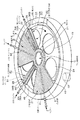
本発明の実施の形態である成膜装置は、図1に示すように平面形状が概ね円形である扁平な真空容器1と、この真空容器1内に設けられ、当該真空容器1の中心に回転中心を有する回転テーブル2と、を備えている。真空容器1は天板11が容器本体12から分離できるように構成されている。天板11は、内部の減圧状態により封止部材例えばOリング13を介して容器本体12側に押し付けられていて気密状態を維持しているが、天板11を容器本体12から分離するときには図示しない駆動機構により上方に持ち上げられる。
As shown in FIG. 1, a film forming apparatus according to an embodiment of the present invention includes a
回転テーブル2は、中心部にて円筒形状のコア部21に固定され、このコア部21は、鉛直方向に伸びる回転軸22の上端に固定されている。回転軸22は真空容器1の底面部14を貫通し、その下端が当該回転軸22を鉛直軸回りにこの例では時計方向に回転させる駆動部23に取り付けられている。回転軸22及び駆動部23は、上面が開口した筒状のケース体20内に収納されている。このケース体20はその上面に設けられたフランジ部分が真空容器1の底面部14の下面に気密に取り付けられており、ケース体20の内部雰囲気と外部雰囲気との気密状態が維持されている。
The rotary table 2 is fixed to a
回転テーブル2の表面部には、図2及び図3に示すように回転方向(周方向)に沿って複数枚例えば5枚のウエハであるウエハを載置するための円形状の載置部をなす凹部24が設けられている。なお図4には便宜上1個の凹部24だけにウエハWを描いてある。ここで図4は、回転テーブル2を同心円に沿って切断しかつ横に展開して示す展開図であり、ウエハを載置する凹部24は、図5に示すようにその直径がウエハWの直径よりも僅かに例えば4mm大きく、またその深さはウエハWの厚みと同等の大きさに設定されている。従ってウエハWを凹部24に落とし込むと、ウエハWの表面と回転テーブル2の表面(ウエハWが載置されない領域)とが揃うことになる。ウエハWの表面と回転テーブル2の表面との間の高さの差が大きいとその段差部分で圧力変動が生じることから、ウエハWの表面と回転テーブル2の表面との高さをそろえることが、膜厚の面内均一性をそろえる観点からの好ましい。ウエハWの表面と回転テーブル2の表面との高さを揃えるとは、同じ高さであるかあるいは両面の差が5mm以内であることをいうが、加工精度などに応じてできるだけ両面の高さの差をゼロに近づけることが好ましい。凹部24の底部には、ウエハWの裏面を支えて当該ウエハWを昇降させるための例えば後述する3本の昇降ピン16(図6参照)が貫通する通過孔が形成されている。
As shown in FIG. 2 and FIG. 3, a circular mounting portion for mounting a plurality of wafers, for example, five wafers, is provided on the surface of the
凹部24の円周部と、載置されたウエハの周縁部との隙間へ、反応ガスや不活性ガスの多量のガスの噴射で、ウエハが吹き上げられる。これを抑制するために凹部24の表面(底面)に、図7(a)(b)に示すように放射状の連通溝24aを具備して、回転サセプタ円周部とウエハ周縁部より吹き込まれたガスを放射状の連通溝とおしてガスを迂回させてウエハの浮揚を抑制するようにしてもよい、また、連通溝の代わりに図7(a)(c)に示すようにして、凸24bを島状に設けてウエハの裏面側にガスの通過空間を確保してもよい。
The wafer is blown up by jetting a large amount of reactive gas or inert gas into the gap between the circumferential portion of the
凹部24はウエハWを位置決めして回転テーブル2の回転に伴なう遠心力により飛び出さないようにするためのものであり、本発明のウエハ載置部に相当する部位であるが、ウエハ載置部は、凹部に限らず例えば回転テーブル2の表面にウエハの周縁をガイドするガイド部材、であってもよい。回転テーブル2には、図13に示すように各凹部24に対応してウエハ昇降用の昇降ピン16が通過するための貫通孔16aと、クランプリング昇降用の昇降ピン17が貫通する貫通孔17aとが形成されている。貫通孔16aは例えば凹部24の底面に3ヶ所形成され、貫通孔17aは凹部の周囲に4ヵ所形成されている。図8は凹部24a及びその周囲部分を示しており、昇降ピン16、17とクランプリング18とを示している。クランプリング18は凹部24の周囲からウエハ載置空間に跨っている幅寸法に形成されると共に例えば凹部24の周方向に沿ったリング状に形成され、昇降ピン17により昇降されるように構成されている。このクランプリング18は昇降ピン17が下降したときに凹部24内のウエハWの表面周縁部に対向して、回転テーブル2の回転時にウエハWの飛び出しを防止する係止部をなすものである。即ち、クランプリング18は昇降ピン17により昇降され、昇降ピン17が下降したときに、凹部24内のウエハWの表面周縁部に接触する。従ってクランプリング18の内径はウエハWの外径よりも小さい。回転テーブル2の停止時においてクランプリング18の下面はウエハの表面に接触していることに限らず、隙間があってもよい、またクランプリング18においてウエハWの表面に係止する部位は、ウエハWの全周に亘っていることに限らず、後述の図11に示すように、リング本体から内方に突出するように複数個所に爪を形成し、この爪によりウエハWを係止する構造であってもよい。
クランプリング18は、図9(a)に示す構造でもよいが、気流を乱しやすいことから、図9(b)に示すようにウエハの表面を流れる反応ガス及び分離ガスの気流を乱す程度が小さい、断面が円弧形状のクランプリングであることが好ましい。
図9に符号24pで示す部材は、回転テーブル2の凹部24の底面に適合する形状の台座(板状部材)である。ウエハWはこの台座24pの上に載置され、台座24Pは回転テーブル2における昇降ピン16の貫通孔16aを塞いでいる。昇降ピン17は、台座24Pを突き上げて台座24pごとウエハWを持ち上げる。台座24pはウエハWよりも小さいサイズに形成されており、外部の搬送アーム10(図3参照)は、台座24pが存在しないウエハWの周縁下面を保持することにより、台座24pとの間の受け渡しを行うことができる。台座24pの重量は、成膜処理が行われているとき回転テーブル2の下方側のパージガスの圧力により浮上しないように設定されている。
図10に、上記クランプリングの形状の他の例を示す。図10(a)(b)(c)は、成膜によって異なる反応ガスの種類によって、最良の形状を選択する事が可能である。
The
The
9 is a pedestal (plate-shaped member) having a shape that fits the bottom surface of the
FIG. 10 shows another example of the shape of the clamp ring. In FIGS. 10A, 10B, and 10C, the best shape can be selected depending on the type of reaction gas that varies depending on the film formation.
クランプリング18はウエハWを、回転テーブル2の回転に伴なう遠心力とチャンバ内に存在する圧力差によるウエハWの浮揚により飛び出さないようにするためのものであり、図11(a)に示すようにリング本体に各々内方に突出する爪25を周方向に複数(図11では4個)間隔をおいて設け、これら爪25によりウエハの周縁部を係止するようにしてもよい。この場合、クランプリング18の内径は、ウエハWの外径よりも大きくし(例えば直径300mmウエハに対して直径300mm+(1mm〜5mm))している。図11(b)は爪25の配置を、回転テーブル2の回転中心を中心とする円(矢印で示す線)上に合わせた位置とし、ガス気流を極力乱さない形状としている。図11に記載した爪25を含むクランプリング18の構造は、図9のクランプリング18に対応しているが、図12に示すクランプリングに対応させる場合には、爪25をなす係止片をクランプリング18の上面に溶接し、この係止片をリング18の内方に突出させる構成とすればよい。図11(c)に示すように反応ガスがウエハ裏面に廻り込みウエハの裏面への成膜を抑制するためにウエハの円周を全て覆う形状を持つクランプリング26の形状もある。図11(c)の形状によれば、反応ガスがウエハWの裏面に回り込んで成膜されることを抑えることができる。これらは、前記に示すよう、反応ガスの種類によって最良の形状を選択する事が可能である。
The
回転テーブル2の表面上を流れる、反応ガス気流を整流するための機構を
図12(a)〜(f)に示す。
図12(a)〜(c)は、回転テーブル2の表面とクランプリングを同一面にする機構、この時、
図12(a)は、ウエハクランプのウエハに接触する面と、ウエハ表面は面接触をしている。
図12(b)は、ウエハクランプのウエハに接触する面と、ウエハ表面は接触をしない。
図12(c)は、ウエハクランプのウエハに接触する面と、ウエハ表面は点接触をするものである。
図12(d)〜(f)は、回転テーブル2とウエハ表面は同一で、ウエハクランプが高くなる機構、この時、
図12(d)は、ウエハクランプのウエハに接触する面と、ウエハ表面は面接触をしている。図12(e)は、ウエハクランプのウエハに接触する面と、ウエハ表面は接触をしない。
図12(f)は、ウエハクランプのウエハに接触する面と、ウエハ表面は点接触をするものである。
FIGS. 12A to 12F show a mechanism for rectifying the reactive gas flow that flows on the surface of the
FIGS. 12A to 12C show a mechanism for making the surface of the rotary table 2 and the clamp ring the same surface,
In FIG. 12A, the surface of the wafer clamp that contacts the wafer and the wafer surface are in surface contact.
In FIG. 12B, the surface of the wafer clamp that contacts the wafer does not contact the wafer surface.
In FIG. 12C, the wafer contact surface of the wafer clamp and the wafer surface are in point contact.
12 (d) to 12 (f) show a mechanism in which the rotary table 2 and the wafer surface are the same and the wafer clamp becomes high,
In FIG. 12D, the surface of the wafer clamp that contacts the wafer and the wafer surface are in surface contact. In FIG. 12E, the surface of the wafer clamp that contacts the wafer does not contact the wafer surface.
In FIG. 12F, the surface of the wafer clamp that contacts the wafer and the surface of the wafer are in point contact.
更に真空容器1の側壁には図2、図3及び図5に示すように外部の搬送アーム10と回転テーブル2との間でウエハであるウエハWの受け渡しを行うための搬送口15が形成されており、この搬送口15は図示しないゲートバルブにより開閉されるようになっている。また回転テーブル2におけるウエハ載置部である載置部の凹部24はこの搬送口15に臨む位置にて搬送アーム10との間でウエハWの受け渡しが行われることから、回転テーブル2のウエハ載置部の下方側において当該受け渡し位置に対応する部位に、載置部の凹部24を貫通してウエハWを裏面から持ち上げるための受け渡し用の昇降ピン16を上下に動かす昇降機構19(図13参照)が設けられる。この昇降機構19は図3に示す制御部100からの制御信号により制御される。
Further, as shown in FIGS. 2, 3, and 5, a
また、ウエハの浮揚を制限するクランプリング18に対しても回転テーブル2の載置部の下方側において当該受け渡し位置に対応する部位に、凹部周辺部を貫通してクランプリング18を裏面から持ち上げるための受け渡し用の昇降ピン17が図13に示すように設けられる。この例では昇降ピン16、17の長さを変え、昇降機構19は昇降ピン16,17に対して共用化されている。
Further, also for the
次に上述実施の形態の作用について説明する。先ず図示しないゲートバルブを開き、外部から搬送アーム10により搬送口15を介してウエハWを回転テーブル2のウエハ載置部、載置部の凹部24内に受け渡す。この受け渡しは、載置部の凹部24が搬送口15に臨む位置に停止したときに図6に示すように載置部の凹部24の底部の貫通孔を介して真空容器の底部側からウエハ昇降ピン16とクランプリング昇降ピン17が昇降することにより行われる。
Next, the operation of the above embodiment will be described. First, a gate valve (not shown) is opened, and the wafer W is transferred from the outside through the
本実施の形態、図5において使用したウエハWの直径は300mmであり、凹部24の直径は304mmである。よって、凹部24がウエハWよりも4mm大きい。遠心力による載置部の凹部24内でのウエハの移動を抑制する為に、移載載置が機械的精度が可能な距離に最初からウエハを円周方向に偏心した形で移載する方法を述べる。ウエハをウエハ昇降ピン16上に載置する前に、図14に示す例えばCCDカメラ104を含む位置検出手段により、凹部24の円周位置を測定して、円周部位置データーを図3に示す制御部100へ送信する。送信された制御部100は、一時保管エリアに凹部円周位置検出データーを保管する。保管された凹部円周位置検出データーを元に、ウエハ移載アームの送り量を、制御部100に保管された凹部円周位置検出データーより円周方向へ載置できる数値を演算した上でアームの送り量を決定して、ウエハをウエハ昇降ピンの上に載置する。載置されたウエハ昇降ピンは、凹部に向かい下降して、ウエハは、凹部24の壁部における回転テーブル2の外周に近い部分に、近づけて載置が可能となる。即ちCCDカメラ104は固定されており、取得した画像の各画素のX−Y方向の位置は、搬送アーム10の駆動系の座標原点に対応する位置になっている。従って凹部の輪郭である円の座標をCCDカメラ104の撮影結果から求めることにより、制御部は、凹部内の所定位置(凹部の中心に対してウエハの中心が回転テーブルの回転に伴う遠心力の作用する方向に変移した位置)にウエハが置かれるように搬送アーム10を制御することになる。この所定位置は制御部のメモリ内に予め記憶されており、ウエハが凹部の側壁に当たるかあるいは極めて近い位置である。
The diameter of the wafer W used in this embodiment, FIG. 5, is 300 mm, and the diameter of the
図13に示すように、本実施の形態では、回転テーブル2のウエハ載置部、載置部の凹部24において、ウエハWの受け渡しのための昇降ピン16を上下方向、及び半径方向に移動させるための昇降機構19が設けられている。この昇降機構19は、図3に示す制御部100からの制御信号に基づき動作の制御がなされる。具体的な動作は、3本の昇降ピン16の昇降させることが可能である。また3本の昇降ピン16を同時に半径方向に移動させるようにしてもよく、この場合には搬送アーム10によりウエハの中心と凹部の中心とを合わせるようにウエハを移載し、その後昇降ピン16によりウエハを持ち上げて昇降させることになる。尚、昇降ピン16のみが上下方向の移動、及び半径方向の移動を行う構成であってもよいし、昇降ピン16及び昇降ピン移動部が一体となって、上下方向の移動を行う構成である。
As shown in FIG. 13, in the present embodiment, the lifting pins 16 for transferring the wafer W are moved in the vertical direction and the radial direction in the wafer mounting portion of the
次に、図15に、本実施の形態におけるウエハWの受け渡しの手順について説明する。尚、本実施の形態において使用したウエハWの直径は300mmであり、載置部の凹部24の直径は304mmである。よって、載置部の凹部24がウエハWよりも4mm大きい。
Next, FIG. 15 illustrates a procedure for transferring the wafer W in the present embodiment. The diameter of the wafer W used in the present embodiment is 300 mm, and the diameter of the
図15(a)は、移載を開始する前の状態で、回転テーブルは、位置検出手段により回転テーブルに開けられた貫通孔にウエハ昇降ピン16、クランプリング昇降ピン17、が通る位置で停止している。搬送アーム10に乗せられているウエハWは、ウエハケース(図示せず)より1枚取り出してきている状態から示す。
FIG. 15A shows a state before the transfer is started, and the rotary table stops at a position where the wafer lifting pins 16 and the clamp ring lifting pins 17 pass through the through holes opened in the rotary table by the position detecting means. doing. The wafer W placed on the
図15(b)は、ウエハ載置部に開けられた通過孔にクランプリング昇降ピン17より入り、図15(c)でクランプリング18を持ち上げる状態になる、同時にウエハ昇降ピン16は、ウエハを受け取る位置で、搬送アーム10に乗せられたウエハWを待つ。図15(d)で、搬送アーム10に乗せられたウエハWは、ウエハ昇降ピン16の真上で停止する。
FIG. 15B shows a state in which the clamp ring raising / lowering
この時、位置検出部で取得した当該ウエハが載置される凹部の円周位置のデータに基づいて、凹部の中心よりも回転テーブルの径方向外側に偏移した位置の真上にウエハが位置するように搬送アーム10の停止位置を制御し次いで搬送アーム10を下降させて図15(e)でウエハ昇降ピン16の上に載置する。ウエハWをウエハ昇降ピンへ移した後に、図15(f)搬送アームは更に下降して、図15(g)の搬送アーム10が引き出せる位置まで下降して、引き抜く。
At this time, based on the data of the circumferential position of the concave portion on which the wafer is placed obtained by the position detection unit, the wafer is positioned directly above the position shifted radially outward of the rotary table from the center of the concave portion. Then, the stop position of the
図15(h)にて搬送アーム10は、回転テーブルより離れ、クランプリング昇降ピン17、ウエハ昇降ピン16は下降を始める、図15(i)でウエハ載置位置にウエハは、載置される。図15(j)で、クランプリング18は、ウエハの円周を係止するように載置される。クランプリング昇降ピン17は、クランプリング18を載置した後、図15(k)で回転テーブル2の下部に戻り、回転テーブル2は回転可能になる。
こうしてこの例では5枚のウエハWが各凹部24内に載置されると、真空容器1内の処理雰囲気が所定の真空度になるように真空排気される。そしてウエハWの温度が所定のプロセス温度に安定する時間が経過した後、あるいはウエハWの温度がプロセス温度に安定したことを図示しない温度検出部で検出した後、回転テーブル2を回転させる。この回転に伴って、第1の反応ガスノズル31及び第2の反応ガスノズル32から例えばBTBASガス及びオゾンガスを夫々供給する。一方分離ガスノズル41、42から分離ガスを供給し、これにより、第1の処理領域P1及び第2の処理領域P2に夫々供給されたBTBASガス及びオゾンガスが凸状部4と回転テーブル2との間の狭隘ない空間から吐出する分離ガス(N2)ガスにより混合が防止される。そしてウエハWは、BTBASガスの吸着と、吸着されたBTBASガスとオゾンガスとの反応が繰り返されて薄膜成分が積層され成膜処理が進行する。
15 (h), the
In this way, in this example, when five wafers W are placed in the
ウエハWは、回転テーブル2の半径方向における外周方向において、回転テーブル2の凹部24の壁面と接触又は近接しているため、回転テーブル2が高速で回転しても、遠心力によりウエハWが回転テーブル2の載置部の凹部24の壁面と強くぶつかることはないため、ウエハWの割れの発生や、カケが生じる可能性は極めて低い。このため、ウエハWと回転テーブル2の載置部の凹部24の壁面との接触することにより生じるパーティクルの発生を防止することができ、これに起因して生じる装置内の環境汚染や成膜される膜中への不純物の混入を防止することができる。
Since the wafer W is in contact with or close to the wall surface of the
またこの実施の形態の成膜装置は、装置全体の動作のコントロールを行うためのコンピュータからなる制御部100が設けられ、この制御部100のメモリ内は装置を運転するためのプログラムが格納されている。このプログラムは後述の装置の動作を実行する用にステップ群が組まれており、ハードディスク、コンパクトディスク、光磁気ディスク、メモリカード、フロッピー(登録商標)ディスクなどの記憶媒体から制御部100内にインストールされる。
Further, the film forming apparatus of this embodiment is provided with a
以上述べた成膜装置を用いたウエハ処理装置について図16に示しておく。図16中、1
01は例えば25枚のウエハを収納するフープと呼ばれる密閉型の搬送容器、102は搬
送アーム103が配置された大気搬送室、104、105は大気雰囲気と真空雰囲気との
間で雰囲気が切り替え可能なロードロック室(予備真空室)、106は、2基の搬送アー
ム107a、107bが配置された真空搬送室、108、109は本発明の成膜装置であ
る。搬送容器101は図示しない載置部を備えた搬入搬出ポートに外部から搬送され、大
気搬送室102に接続された後、図示しない開閉機構により蓋が開けられて搬送アーム1
03により当該搬送容器101内からウエハが取り出される。次いでロードロック室10
4(105)内に搬入され当該室内を大気雰囲気から真空雰囲気に切り替え、その後搬送
アーム107a又は107bによりウエハが取り出されて成膜装置108、109の一方
に搬入され、既述の成膜処理がされる。このように例えば5枚処理用の本発明の成膜装置
を複数個例えば2個備えることにより、いわゆるALD(MLD)を高いスループットで
実施することができる。
A wafer processing apparatus using the film forming apparatus described above is shown in FIG. In FIG. 16, 1
For example, 01 is a sealed transfer container called a hoop for storing 25 wafers, 102 is an atmospheric transfer chamber in which a
03, the wafer is taken out from the
4 (105) and the room is switched from the atmospheric atmosphere to the vacuum atmosphere. Thereafter, the wafer is taken out by the
以上のような成膜装置の構成においてウエハが飛び出す原因として考えられることは、図17に示すとおり、気流の流れの存在が考えられる。
例えば、反応領域P1の反応ガスはBTBASでこの場合、100sccm、反応領域P2の反応ガスはオゾンの場合、10slm、この時の各々反応領域を分離するための分離ガスは、10slm、さらに中心部より反応ガスの混合を防ぐために中心部よりも10slmを流す。また、チャンバ圧力は8torr、回転テーブルの回転数は、240rpmとすると、反応ガス、分離ガスは図17に示す矢印のような流れを形成する。
同時に、チャンバ内は、各々の圧力が異なり、ウエハを係止しないで回転テーブルに載置するとウエハは浮揚して破損するおそれがある。
One possible cause of the wafer jumping out in the configuration of the film forming apparatus as described above is the presence of an air flow as shown in FIG.
For example, the reaction gas in the reaction zone P1 is BTBAS, in this
At the same time, the pressure in the chamber is different, and if the wafer is placed on the rotary table without being locked, the wafer may float and be damaged.
第17図を用いて本件他の実施例の成膜装置の特徴を述べる。この例は、凹部24、昇降ピン16,17クランプリング18の構造やウエハの移載の手法については先の実施形態と全く同じである。
成膜装置の複数の処理領域のうち第二の処理領域P2の面積が、第一の処理領域P1の面積に比較して2倍以上大きく、具体的には回転中心から見た扇形のP2の中心角度が約180度となっている。更に、この第二処理領域P2における第二の反応ノズル32の位置が、回転テーブルの回転方向の上流側前半の中に位置しており、排気領域6が下流側下流側後半に位置し、この排気領域62の中に、排気口62が設けられている。
この構成を取ることにより分離領域Dの約中央に配置された分離ガスノズル42,41から供給された窒素ガスと、第二の反応ガスノズルから供給したオゾンがスとが共に実線矢印の通り排気される。
この気流の流れは回転テーブルに保持されて回転するウエハ表面に於いて、第一の処理領域P1で第一の反応ガスノズル殻供給されたBTBASガスが
前記ウエハ表面に吸着された状態で、第二の処理領域の内部に入ってきて、最も長い時間、オゾンガスが前記ウエハに対して供給され、BTBASガスとオゾンガスによる酸化反応が、約180度の中心角度を持つ扇形の処理領域を時間を要して通過することで反応を促進するのに適した時間的・空間的処理空間を提供することが出来、一回転あたりの成膜速度を大きく向上させることが出来る。従って均等割りした同じ面積の処理空間を複数も受ける技術に比較して成膜速度が向上できる技術を提供できる。
The characteristics of the film forming apparatus according to another embodiment will be described with reference to FIG. In this example, the structure of the
Of the plurality of processing regions of the film forming apparatus, the area of the second processing region P2 is more than twice as large as the area of the first processing region P1, more specifically, the fan-shaped P2 viewed from the center of rotation. The center angle is about 180 degrees. Further, the position of the
By adopting this configuration, the nitrogen gas supplied from the
The air flow is held on the rotary table and rotated on the surface of the wafer while the BTBAS gas supplied to the first reaction gas nozzle shell in the first processing region P1 is adsorbed on the wafer surface. The ozone gas is supplied to the wafer for the longest time, and the oxidation reaction with the BTBAS gas and the ozone gas takes a long time for the fan-shaped processing region having a central angle of about 180 degrees. By passing through, it is possible to provide a temporal and spatial processing space suitable for promoting the reaction, and the film formation rate per rotation can be greatly improved. Therefore, it is possible to provide a technique capable of improving the film formation speed as compared with a technique that receives a plurality of equally divided processing spaces having the same area.
第17図に於いて、回転中心Cからは、不活性ガスが実線矢印の通り放射状に真空容器内部に供給されているので、処理領域に供給されるプロセスガスが回転中心に存在する回転テーブルの回転機構のメカに作用して反応副生成物を付着させたり、酸化作用というメカによくない作用を避けることができる、更に中央から供給される不活性ガスは前記分離領域Dから供給される不活性ガスと共同して一体化して、処理領域に供給されるプロセスガスが、ウエハ表面以外の真空容器内部で混合し、反応することを防止している。 In FIG. 17, since the inert gas is supplied radially from the rotation center C to the inside of the vacuum vessel as indicated by the solid line arrow, the process gas supplied to the processing region is at the rotation center. The reaction by-product can be adhered by acting on the mechanism of the rotation mechanism, and an adverse effect on the mechanism such as oxidation can be avoided. Further, the inert gas supplied from the center is not supplied from the separation region D. The process gas that is integrated with the active gas and supplied to the processing region is prevented from mixing and reacting inside the vacuum vessel other than the wafer surface.
ALDプロセスの第一のプロセスガスは、BTBASを使用して、第一反応ノズル31から、真空容器内の第一の処理領域P1の内部に導入される。第一の反応ノズルを真空容器の側壁8チャンバウォール)から回転テーブルの中心領域Cに導入する構成とすることで、第一の処理領域P1の内部を流れるガスの流れ(実線の矢印)を遮ることが最小限となり、前記気流の流れがスムーズに第一の処理領域P1を横断して、第一の処理領域の外周側であり、かつ回転テーブルの外周側に設けられた排気領域6の中の排気口61の中に流れることを達成するが出来る効果がある。第一の処理領域の回転テーブル2における両側には、二つの分離領域Dがそれぞれ設けられている。これらの分離領域の中央には窒素ガスノズル41及び42が設けられ不活性ガスであるN3が回転テーブルの方向に噴射される構成となっている。不活性ガスは分離領域Dと回転テーブル2との間に設けられたきわめて狭隘な空間の中で広がり、隣接する第一の処理領域P1と第二の処理領域P2の方向に排気される気流の流れを形成して、前記処理ガスに供給されるプロセスガスが分離領域Dの中に入り込前記狭隘な空間のなかで反応しない構成となって入る。この技術は発明者らの創意工夫の結果、分離領域の外周側であって、かつ回転テーブル2の外周側における真空容器の側壁(チャンバーウォール)と分離領域との間の隙間を、回転テーブルがスムーズに回転するには十分な間隔ではあるが、ガスの排気空間としては働きにくい狭い隙間とすることと、第一の処理領域P1の外周に設けた排気口61と第二の処理領域P2の外周に設けた排気口62の方向に、処理領域内に於いて供給されるプロセスガスと隣接する分離領域から供給される不活性ガス(窒素ガス)の両者を排気することで達成できることを見出した。この両者のガスを排気口61,62に流す気流の流れ(第17図の実線の矢印で図面中に記載してある)により、次の3つの効果を達成することが出来る。
第一の効果:反応ガスノズル31,32から供給されたプロセスガスが回転テーブル上に載置されたウエハに供給され表面反応に使用されると、ノズルの配置に対して、交差する方向で前記ガスの気流の流れが形成されるので、常にウエハ上に新たなガスを供給することが出来る。言い換えると隣接したノズル内の開口孔から供給されるプロセスガスを使用済みのガス(反応に使用されたガス)により新たに供給されるプロセスガスが邪魔されない。
第二の効果:処理領域に供給されたプロセスガスが、分離領域の中に入り込んで、反応を起こすことをなくすことが出来る。
第三の効果:第二反応ノズルから供給されるガスが、第二処理領域の中で流れを形成することにより、第一処理領域よりも広い面積で構成された第二処理領域の面積内で期間をかけて、ALD反応の成膜処理を回転テーブル上に載置されたウエハの上で実行できる。従って、同じ回転数の中で比較的高速な成膜速度を達成できる成膜装置を構成して提供できる。
The first process gas of the ALD process is introduced from the
First effect: When the process gas supplied from the
Second effect: The process gas supplied to the processing region can be prevented from entering the separation region and causing a reaction.
Third effect: The gas supplied from the second reaction nozzle forms a flow in the second processing region, so that within the area of the second processing region that is configured with a larger area than the first processing region. Over time, the ALD reaction film formation process can be performed on the wafer placed on the rotary table. Therefore, it is possible to configure and provide a film forming apparatus that can achieve a relatively high film forming speed at the same rotational speed.
以上のように高速な回転、例えば240rpmで成膜を実施すると、各ウエハに対して低速な回転、例えば10乃至30rpmで成膜を実施するときに比べて大きな遠心力が働き、ウエハを収納している回転テーブル2表面に設けた凹部の中でウエハが移動したり、浮き上がり、振動したり、最後には飛び出す現象を引き起こす恐れがある。
そこで本件特許の発明者は、ウエハに及ぼすこれらの現象の原因を明確にするために、真空容器の天板11を透明なアクリル板に変更してプロセス条件下でウエハの様子を真空容器の上部より観察した結果、ウエハの浮き上がり、振動、飛び出しが発生する原因が、上記遠心力と共に、ウエハが回転テーブルの回転に伴い、真空容器を構成する分離領域から処理領域にさしかかったときにウエハが受けるガス圧力の差、言い換えると各領域に供給されるガス流量の差異がウエハに及ぼす影響が加算して、これらの減少を生じる原因であることを観察した。
これらの複合的な原因に基づくウエハの飛び出し、移動、ぶつかり、振動の中で特に飛び出しに対して、少なくとも回転テーブルのウエハを収納する凹部の近傍に、ウエハが飛び出すことを防止する係止手段を設けることが良いとの結論を得るに至った。実施例のプロセス条件ではプロセスガスとして、BTBAS:100sccm、オゾン:10slm、窒素:10slmを流してSiO2膜の成膜を行ったため、ガス流量の単位がsccmオーダーとslmオーダーという1000倍の差からも分かるとおり大きな流量の差が分離領域と処理領域との境界を挟んで生じていたため、このような観察結果を得たものと考えられる。このような大きな圧力差が同じ真空容器内部に存在している環境は、
プロセスを行う処理領域がお互いに連通してはいるが、不活性ガスを流している狭隘な空間を複数の処理領域の間に作ることにより、複数のプロセスガスの流れとしてはお互いに分離されている状態を形成できる技術により達成できた。更に成膜速度大幅に向上する技術として、ウエハを載置している回転テーブルを240rpmという高速回転しても、前記分離領域の機能を維持できる構成を実現することに成功した。
As described above, when film formation is performed at a high speed, for example, 240 rpm, a large centrifugal force is exerted on each wafer compared to when film formation is performed at a low speed, for example, 10 to 30 rpm. There is a possibility that the wafer moves, floats, vibrates, or finally jumps out in a recess provided on the surface of the
Therefore, in order to clarify the cause of these phenomena on the wafer, the inventor of the present patent changed the
Locking means for preventing the wafer from popping out at least in the vicinity of the recess of the rotary table for accommodating the wafer, particularly against the popping out, movement, collision and vibration of the wafer based on these complex causes. It came to the conclusion that it was good to install. Since the SiO2 film was formed by flowing BTBAS: 100 sccm, ozone: 10 slm, nitrogen: 10 slm as process gases under the process conditions of the example, the unit of gas flow rate is also 1000 times difference between sccm order and slm order. As can be seen, a large flow rate difference occurred across the boundary between the separation region and the processing region, and it is considered that such an observation result was obtained. The environment where such a large pressure difference exists inside the same vacuum vessel is
Although the processing areas where the process is performed are in communication with each other, the process gas flows are separated from each other by creating a narrow space where an inert gas flows between the processing areas. This can be achieved by a technology that can form a certain state. Furthermore, as a technique for greatly improving the film forming speed, the present inventors have succeeded in realizing a configuration capable of maintaining the function of the separation region even when the rotary table on which the wafer is placed is rotated at a high speed of 240 rpm.
本発明は
回転式ミニバッチALD装置において、回転テーブルに載置されたウエハが浮揚する事を抑制するために、
(1)ウエハWの係止にあたり、4種類の構造を持つ、
(2)爪形状は、3種類あり ウエハの一部を係止する方法、また、爪は、回転テーブルの円弧と同じ曲率に向けたものと、と全周にわたり爪形状をなして係止する。
(3)ウエハ裏面、回転テーブル凹部に空気抜き溝および凸状構造物を設けて、ウエハノズルから直接噴射するガスを他方へ逃がす構造。
(4)上記の回転テーブル凹部の空気抜き溝及び凸状構造物を別体として回転テーブル凹部にペデスタル載置して、そのペデスタルに上記溝および凸状構造物を設ける。
(5)ウエハクランプ及び爪形状の構造物に空気抵抗緩和のための流線型形状を施す。
(6)ウエハクランプ及び爪形状の構造物とウエハ表面の高さ位置関係と遠心力を想定した円周方向へのウエハ載置を行なう。
In the rotary mini-batch ALD apparatus, the present invention suppresses the floating of the wafer placed on the rotary table.
(1) There are four types of structures for locking the wafer W.
(2) There are three types of claw shapes. A method for locking a part of the wafer, and a claw that locks in the same curvature as that of the arc of the rotary table and locks the claw shape over the entire circumference. .
(3) A structure in which an air vent groove and a convex structure are provided on the back surface of the wafer and on the concave portion of the rotary table, and the gas directly injected from the wafer nozzle is released to the other side.
(4) The air vent groove and the convex structure of the rotary table recess are separately mounted on the rotary table recess, and the groove and the convex structure are provided on the pedestal.
(5) A streamlined shape for reducing air resistance is applied to the wafer clamp and the claw-shaped structure.
(6) Wafer mounting in the circumferential direction assuming a wafer clamp and claw-shaped structure and the height positional relationship between the wafer surface and centrifugal force.
本発明の実施形態による成膜装置は、酸化シリコン膜の成膜に限らず、窒化シリコンの分子層成膜にも適用することができる。また、トリメチルアルミニウム(TMA)とO3ガスを用いた酸化アルミニウム(Al2O3)の分子層成膜、テトラキスエチルメチルアミノジルコニウム(TEMAZr)とO3ガスを用いた酸化ジルコニウム(ZrO2)の分子層成膜、テトラキスエチルメチルアミノハフニウム(TEMAHf)とO3ガスを用いた酸化ハフニウム(HfO2)の分子層成膜、ストロンチウムビステトラメチルヘプタンジオナト(Sr(THD)2)とO3ガスを用いた酸化ストロンチウム(SrO)の分子層成膜、チタニウムメチルペンタンジオナトビステトラメチルヘプタンジオナト(Ti(MPD)(THD))とO3ガスを用いた酸化チタニウム(TiO)の分子層成膜などを行うことができる。また、O3ガスではなく、酸素プラズマを利用することも可能である。これらのガスの組み合わせを用いても、上述の効果が奏されることは言うまでもない。
以上、本発明を実施形態により説明したが、本発明は上記実施形態に限定されるものではなく、本発明の範囲内で種々の変形及び改良が可能であることは言うまでもない。
The film forming apparatus according to the embodiment of the present invention can be applied not only to the formation of a silicon oxide film but also to the formation of a molecular layer of silicon nitride. Also, molecular layer deposition of aluminum oxide (Al 2 O 3 ) using trimethylaluminum (TMA) and O 3 gas, zirconium oxide (ZrO 2 ) using tetrakisethylmethylaminozirconium (TEMAZr) and O 3 gas. Molecular layer deposition, molecular layer deposition of hafnium oxide (HfO 2 ) using tetrakisethylmethylaminohafnium (TEMAHf) and O 3 gas, strontium bistetramethylheptanedionate (Sr (THD) 2 ) and O 3 gas Strontium oxide (SrO) molecular layer film formation using titanium, titanium oxide (TiO) molecular layer formation using titanium methylpentanedionatobistetramethylheptanedionate (Ti (MPD) (THD)) and O 3 gas A membrane or the like can be performed. It is also possible to use oxygen plasma instead of O 3 gas. It goes without saying that the above-described effects can be achieved even if a combination of these gases is used.
As mentioned above, although this invention was demonstrated by embodiment, it cannot be overemphasized that this invention is not limited to the said embodiment, A various deformation | transformation and improvement are possible within the scope of the present invention.
1 真空容器
10 搬送アーム
11 天板
12 容器本体
15 搬送口回転テーブル
16 昇降ピン
2 回転テーブル
21 コア部
24 凹部(ウエハ載置部)
31 第1の反応ガスノズル
32 第2の反応ガスノズル
P1 第1の処理領域
P2 第2の処理領域
D 分離領域
C 中心部領域
4 凸状部
41、42 分離ガスノズル
44 第1天井面
45 第2の天井面
5 突出部
51 分離ガス供給管
6 排気領域
61、62 排気口
7 ヒータユニット
72、73 パージガス供給管
W ウエハ
DESCRIPTION OF
31 1st
Claims (9)
前記真空容器内に設けられた回転テーブルと、
前記回転テーブルに基板を載置するために設けられた基板載置部と、
前記回転テーブルの回転方向に互いに離れて設けられ、前記回転テーブルにおける前記基板の載置領域側の面に夫々第1の反応ガス及び第2の反応ガスを供給するための第1の反応ガス供給手段及び第2の反応ガス供給手段と、
前記第1の反応ガスが供給される第1の処理領域と第2の反応ガスが供給される第2の処理領域との雰囲気を分離するために、これら処理領域の間に位置する分離領域と、
予め設定された受渡し位置に停止している基板載置部に対して基板の受け渡しを行うための搬送機構と、
前記基板載置部に載置された基板の飛び出しを防止するために基板の表面を係止する係止部と、
前記回転テーブルとは別個に設けられ、基板の受け渡し時に回転テーブルより下方に離れた位置から回転テーブル内を貫通して回転テーブルと回転テーブルよりも上方位置との間で基板及び係止部を夫々昇降させるための基板用の昇降ピン及び係止部用の昇降ピンを含む昇降機構と、
前記回転テーブルに設けられ、前記基板用の昇降ピンが通る孔部及び前記係止部用の昇降ピンが通る孔部と、を備え、
前記基板用の昇降ピン及び前記係止部用の昇降ピンは、回転テーブルよりも下方側で待機するように構成されていることを特徴とする成膜装置。 In a film forming apparatus for forming a thin film by laminating a number of reaction product layers by sequentially supplying at least two kinds of reaction gases that react with each other in a vacuum vessel to the surface of a substrate and executing this supply cycle ,
A rotary table provided in the vacuum vessel;
A substrate mounting portion provided for mounting the substrate on the rotary table;
A first reaction gas supply that is provided apart from each other in the rotation direction of the turntable and supplies a first reaction gas and a second reaction gas to a surface of the turntable on the substrate mounting region side, respectively. Means and second reactive gas supply means;
In order to separate the atmosphere of the first processing region supplied with the first reaction gas and the second processing region supplied with the second reaction gas, a separation region located between these processing regions; ,
A transport mechanism for delivering a substrate to a substrate platform that is stopped at a preset delivery position ;
A locking portion for locking the surface of the substrate to prevent the substrate mounted on the substrate mounting portion from popping out;
Provided separately from the rotary table, the substrate and the locking portion are respectively passed between the rotary table and a position above the rotary table through the rotary table from a position below the rotary table when the board is transferred. An elevating mechanism including an elevating pin for a substrate for raising and lowering and an elevating pin for a locking portion ;
A hole that is provided on the rotary table and through which the lift pin for the substrate passes and a hole through which the lift pin for the locking portion passes;
The substrate raising and lowering pins and the locking portion raising and lowering pins are configured to stand by below the rotary table .
前記処理領域の天井から離間し前記基板の近傍に設けられ、前記基板の方向に向けて反応ガスを供給する反応ガス供給手段と、
前記異なる反応ガスが反応することを防止する不活性ガスを、前記複数の処理領域の間に設けられた分離空間内に供給する不活性ガス供給手段と、
前記複数の処理領域のそれぞれに対応して設けられ、前記回転テーブルの外側に設けられた排気口と、
前記処理領域に供給した反応ガスと前記分離領域に供給した不活性ガスとを前記処理領域を経由して前記排気口に導き前記真空容器から排気する真空排気手段と、
前記回転テーブルに設けられた前記各凹部の近傍に設けられ、前記基板が前記回転テーブルの回転中に飛び出すことを防止するために基板の表面を係止する係止部と、
前記回転テーブルとは別個に設けられ、外部の搬送機構による基板の受け渡し時に回転テーブルより下方に離れた位置から回転テーブル内を貫通して回転テーブルと回転テーブルよりも上方位置との間で基板及び係止部を夫々昇降させるための基板用の昇降ピン及び係止部用の昇降ピンを含む昇降機構と、
前記回転テーブルに設けられ、前記基板用の昇降ピンが通る孔部及び前記係止部用の昇降ピンが通る孔部と、を備え、
前記基板用の昇降ピン及び前記係止部用の昇降ピンは、回転テーブルよりも下方側で待機するように構成されていることを特徴とする成膜装置。 In the vacuum vessel, by placing and rotating a plurality of substrates in a plurality of recesses provided on the surface of the turntable, respectively, the substrates are sequentially brought into contact with the reaction gases supplied to a plurality of different processing regions, In a film forming apparatus for forming a thin film on the surface of the substrate,
A reaction gas supply means that is provided in the vicinity of the substrate apart from the ceiling of the processing region and supplies a reaction gas toward the substrate;
An inert gas supply means for supplying an inert gas for preventing the different reaction gases from reacting into a separation space provided between the plurality of processing regions;
An exhaust port provided corresponding to each of the plurality of processing regions, and provided on the outside of the rotary table ;
A vacuum exhaust means you exhausted from the vacuum vessel guided to the exhaust port and an inert gas supplied to the reaction gas supplied to the processing region and the isolation region by way of the processing region,
A locking portion that is provided in the vicinity of each of the recesses provided on the turntable, and that locks the surface of the substrate to prevent the substrate from popping out during rotation of the turntable ;
The rotary table is provided separately from the rotary table, passes through the rotary table from a position below the rotary table when the board is transferred by an external transport mechanism, and passes between the rotary table and the position above the rotary table. An elevating mechanism including an elevating pin for a substrate and an elevating pin for an engaging part for raising and lowering the engaging part , and
A hole that is provided on the rotary table and through which the lift pin for the substrate passes and a hole through which the lift pin for the locking portion passes;
The substrate raising and lowering pins and the locking portion raising and lowering pins are configured to stand by below the rotary table .
前記真空容器の側壁から前記回転テーブルの回転中心に向けて配置され、前記処理領域の天井から離間し前記基板の近傍に設けられ、前記基板の方向に向けて反応ガスを供給する反応ガス供給手段と、
前記異なる反応ガスが反応することを防止する不活性ガスを、前記複数の処理領域の間に設けられた分離空間内において前記回転テーブルに載置された基板方向に向けて吐出する不活性ガス供給手段と、
前記複数の処理領域のそれぞれに対応して設けられ、前記回転テーブルの外側に設けられた排気口と、
前記処理領域に供給した反応ガスと前記分離領域に供給した不活性ガスとを前記処理領域を経由して前記排気口に導き前記真空容器から排気する真空排気手段と、
前記回転テーブルに設けられた前記凹部の近傍に設けられ、前記基板が前記回転テーブルの回転中に飛び出すことを防止する係止部と、
前記回転テーブルとは別個に設けられ、外部の搬送機構による基板の受け渡し時に回転テーブルより下方に離れた位置から回転テーブル内を貫通して回転テーブルと回転テーブルよりも上方位置との間で基板及び係止部を夫々昇降させるための基板用の昇降ピン及び係止部用の昇降ピンを含む昇降機構と、
前記回転テーブルに設けられ、前記基板用の昇降ピンが通る孔部及び前記係止部用の昇降ピンが通る孔部と、を備え、
前記基板用の昇降ピン及び前記係止部用の昇降ピンは、回転テーブルよりも下方側で待機するように構成され、
前記係止部は、凹部内に載置された基板に対して非接触の状態で配置され、基板の飛び出しに際して係止するように構成されていることを特徴とする成膜装置。 In the vacuum vessel, by placing and rotating a plurality of substrates in a plurality of recesses provided on the surface of the turntable, respectively, the substrates are sequentially brought into contact with the reaction gases supplied to a plurality of different processing regions, In a film forming apparatus for forming a thin film on the surface of the substrate,
Reactive gas supply means that is arranged from the side wall of the vacuum vessel toward the rotation center of the turntable, is spaced from the ceiling of the processing area, is provided in the vicinity of the substrate, and supplies the reactive gas toward the substrate. When,
An inert gas supply that discharges an inert gas that prevents the different reaction gases from reacting toward a substrate mounted on the rotary table in a separation space provided between the plurality of processing regions. Means,
An exhaust port provided corresponding to each of the plurality of processing regions, and provided on the outside of the rotary table ;
A vacuum exhaust means you exhausted from the vacuum vessel guided to the exhaust port and an inert gas supplied to the reaction gas supplied to the processing region and the isolation region by way of the processing region,
A locking portion that is provided in the vicinity of the recess provided in the turntable and prevents the substrate from popping out during rotation of the turntable ;
The rotary table is provided separately from the rotary table, passes through the rotary table from a position below the rotary table when the board is transferred by an external transport mechanism, and passes between the rotary table and the position above the rotary table. An elevating mechanism including an elevating pin for a substrate and an elevating pin for an engaging part for raising and lowering the engaging part , and
A hole that is provided on the rotary table and through which the lift pin for the substrate passes and a hole through which the lift pin for the locking portion passes;
The raising / lowering pins for the substrate and the raising / lowering pins for the locking portion are configured to stand by on the lower side than the rotary table,
The film forming apparatus, wherein the locking portion is arranged in a non-contact state with respect to the substrate placed in the recess, and is configured to lock when the substrate jumps out.
前記処理領域の天井から離間し前記基板の近傍に設けられ、前記基板の方向に向けて反応ガスを供給する反応ガス供給手段と、
前記異なる反応ガスが反応することを防止する不活性ガスを、前記複数の処理領域の間に設けられた分離空間内に供給する不活性ガス供給手段と、
前記複数の処理領域のそれぞれに対応して設けられ、前記回転テーブルの外側に設けられた排気口と、
前記処理領域に供給した反応ガスと前記分離領域に供給した不活性ガスとを前記処理領域を経由して前記排気口に導き前記真空容器から排気する真空排気手段と、
前記回転テーブルに設けられた前記各凹部の近傍に設けられ、前記基板が前記回転テーブルの回転中に飛び出すことを防止するために基板の表面を係止する係止部と、
前記回転テーブルとは別個に設けられ、外部の搬送機構による基板の受け渡し時に回転テーブルより下方に離れた位置から回転テーブル内を貫通して回転テーブルと回転テーブルよりも上方位置との間で基板及び係止部を夫々昇降させるための基板用の昇降ピン及び係止部用の昇降ピンを含む昇降機構と、
前記回転テーブルに設けられ、前記基板用の昇降ピンが通る孔部及び前記係止部用の昇降ピンが通る孔部と、
前記回転テーブルの回転の前に、前記基板を、基板の中心が前記凹部の中心に対して、前記回転テーブルの回転に伴う遠心力の方向に偏移した位置になるように制御を行なう制御部と、を備え、
前記基板用の昇降ピン及び前記係止部用の昇降ピンは、回転テーブルよりも下方側で待機するように構成されていることを特徴とする成膜装置。 In the vacuum vessel, by placing and rotating a plurality of substrates in a plurality of recesses provided on the surface of the turntable, respectively, the substrates are sequentially brought into contact with the reaction gases supplied to a plurality of different processing regions, In a film forming apparatus for forming a thin film on the surface of the substrate,
A reaction gas supply means that is provided in the vicinity of the substrate apart from the ceiling of the processing region and supplies a reaction gas toward the substrate;
An inert gas supply means for supplying an inert gas for preventing the different reaction gases from reacting into a separation space provided between the plurality of processing regions;
An exhaust port provided corresponding to each of the plurality of processing regions, and provided on the outside of the rotary table ;
A vacuum exhaust means you exhausted from the vacuum vessel guided to the exhaust port and an inert gas supplied to the reaction gas supplied to the processing region and the isolation region by way of the processing region,
A locking portion that is provided in the vicinity of each of the recesses provided on the turntable, and that locks the surface of the substrate to prevent the substrate from popping out during rotation of the turntable;
The rotary table is provided separately from the rotary table, passes through the rotary table from a position below the rotary table when the board is transferred by an external transport mechanism, and passes between the rotary table and the position above the rotary table. An elevating mechanism including an elevating pin for a substrate and an elevating pin for an engaging part for raising and lowering the engaging part , and
A hole provided in the rotary table, through which the lifting pin for the substrate passes and a hole through which the lifting pin for the locking portion passes;
Before the rotation of the turntable, a control unit that controls the substrate so that the center of the substrate is shifted in the direction of the centrifugal force accompanying the rotation of the turntable with respect to the center of the recess. and, with a,
The substrate raising and lowering pins and the locking portion raising and lowering pins are configured to stand by below the rotary table .
前記処理領域の天井から離間し前記基板の近傍に設けられ、前記基板の方向に向けて反応ガスを供給する反応ガス供給手段と、
前記異なる反応ガスが反応することを防止する不活性ガスを、前記複数の処理領域の間に設けられた分離空間内に供給する不活性ガス供給手段と、
前記複数の処理領域のそれぞれに対応して設けられ、前記回転テーブルの外側に設けられた排気口と、
前記処理領域に供給した反応ガスと前記分離領域に供給した不活性ガスとを前記処理領域を経由して前記排気口に導き前記真空容器から排気する真空排気手段と、
前記回転テーブルに設けられた前記各凹部の近傍に設けられ、前記基板の表面の外周部に接触して前記基板を係止することで、前記基板が回転中に前記凹部から飛び出すことを防止する係止部と、
前記回転テーブルとは別個に設けられ、外部の搬送機構による基板の受け渡し時に回転テーブルより下方に離れた位置から回転テーブル内を貫通して回転テーブルと回転テーブルよりも上方位置との間で基板及び係止部を夫々昇降させるための基板用の昇降ピン及び係止部用の昇降ピンを含む昇降機構と、、
前記回転テーブルに設けられ、前記基板用の昇降ピンが通る孔部及び前記係止部用の昇降ピンが通る孔部と、を備え、
前記基板用の昇降ピン及び前記係止部用の昇降ピンは、回転テーブルよりも下方側で待機するように構成されていること、を特徴とする成膜装置。 In the vacuum vessel, by placing and rotating a plurality of substrates in a plurality of recesses provided on the surface of the turntable, respectively, the substrates are sequentially brought into contact with the reaction gases supplied to a plurality of different processing regions, In a film forming apparatus for forming a thin film on the surface of the substrate,
A reaction gas supply means that is provided in the vicinity of the substrate apart from the ceiling of the processing region and supplies a reaction gas toward the substrate;
An inert gas supply means for supplying an inert gas for preventing the different reaction gases from reacting into a separation space provided between the plurality of processing regions;
An exhaust port provided corresponding to each of the plurality of processing regions, and provided on the outside of the rotary table ;
A vacuum exhaust means you exhausted from the vacuum vessel guided to the exhaust port and an inert gas supplied to the reaction gas supplied to the processing region and the isolation region by way of the processing region,
Provided in the vicinity of each of the recesses provided on the turntable and contacting the outer peripheral portion of the surface of the substrate to lock the substrate, thereby preventing the substrate from jumping out of the recess during rotation. A locking part ;
The rotary table is provided separately from the rotary table, passes through the rotary table from a position below the rotary table when the board is transferred by an external transport mechanism, and passes between the rotary table and the position above the rotary table. A lifting mechanism including a lifting pin for the substrate and a lifting pin for the locking part for raising and lowering the locking part ,
A hole that is provided on the rotary table and through which the lift pin for the substrate passes and a hole through which the lift pin for the locking portion passes;
The substrate raising / lowering pin and the locking portion raising / lowering pin are configured to stand by on the lower side of the rotary table .
前記処理領域の天井から離間し前記回転テーブルの近傍に設けられ、前記回転テーブルの方向に向けて反応ガスを供給する反応ガス供給手段と、
前記異なる反応ガスが反応することを防止する不活性ガスを、前記複数の処理領域の間に設けられた分離空間内に供給する不活性ガス供給手段と、
前記回転テーブルの回転中心から前記真空容器内に不活性ガスを供給する不活性ガス供給手段と
前記複数の処理領域のそれぞれに対応して設けられ、前記回転テーブルの外側に設けられた排気口と、
前記処理領域に供給した反応ガスと前記分離領域に供給した不活性ガスと前記回転中心から供給される不活性ガスとを前記処理領域を経由して前記排気口に導き前記真空容器から排気する真空排気手段と、
前記各凹部の近傍に設けられ、前記基板が前記回転テーブルの回転中に飛び出すことを防止するために基板の表面を係止する係止部と、
前記回転テーブルとは別個に設けられ、外部の搬送機構による基板の受け渡し時に回転テーブルより下方に離れた位置から回転テーブル内を貫通して回転テーブルと回転テーブルよりも上方位置との間で基板及び係止部を夫々昇降させるための基板用の昇降ピン及び係止部用の昇降ピンを含む昇降機構と、
前記回転テーブルに設けられ、前記基板用の昇降ピンが通る孔部及び前記係止部用の昇降ピンが通る孔部と、を備え、
前記基板用の昇降ピン及び前記係止部用の昇降ピンは、回転テーブルよりも下方側で待機するように構成されていることを特徴とする成膜装置。 In the vacuum vessel, by placing and rotating a plurality of substrates in a plurality of recesses provided on the surface of the turntable, respectively, the substrates are sequentially brought into contact with the reaction gases supplied to a plurality of different processing regions, In a film forming apparatus for forming a thin film on the surface of the substrate,
A reaction gas supply means that is provided in the vicinity of the turntable and spaced from the ceiling of the processing region, and supplies a reaction gas toward the turntable;
An inert gas supply means for supplying an inert gas for preventing the different reaction gases from reacting into a separation space provided between the plurality of processing regions;
An inert gas supply means for supplying an inert gas from the rotation center of the rotary table into the vacuum vessel, an exhaust port provided outside the rotary table, provided corresponding to each of the plurality of processing regions ; ,
Exhausted from the vacuum vessel guided to the exhaust port and an inert gas supplied from the rotation center and the inert gas supplied to the isolation region and the reactive gas supplied to the processing region through the processing region and vacuum exhaust means,
A locking portion that is provided in the vicinity of each of the recesses and that locks the surface of the substrate to prevent the substrate from popping out during rotation of the turntable ;
The rotary table is provided separately from the rotary table, passes through the rotary table from a position below the rotary table when the board is transferred by an external transport mechanism, and passes between the rotary table and the position above the rotary table. An elevating mechanism including an elevating pin for a substrate and an elevating pin for an engaging part for raising and lowering the engaging part , and
A hole that is provided on the rotary table and through which the lift pin for the substrate passes and a hole through which the lift pin for the locking portion passes;
The substrate raising and lowering pins and the locking portion raising and lowering pins are configured to stand by below the rotary table .
Priority Applications (1)
| Application Number | Priority Date | Filing Date | Title |
|---|---|---|---|
| JP2010286514A JP5527197B2 (en) | 2009-12-25 | 2010-12-22 | Deposition equipment |
Applications Claiming Priority (3)
| Application Number | Priority Date | Filing Date | Title |
|---|---|---|---|
| JP2009296182 | 2009-12-25 | ||
| JP2009296182 | 2009-12-25 | ||
| JP2010286514A JP5527197B2 (en) | 2009-12-25 | 2010-12-22 | Deposition equipment |
Publications (3)
| Publication Number | Publication Date |
|---|---|
| JP2011151387A JP2011151387A (en) | 2011-08-04 |
| JP2011151387A5 JP2011151387A5 (en) | 2012-10-04 |
| JP5527197B2 true JP5527197B2 (en) | 2014-06-18 |
Family
ID=44172785
Family Applications (1)
| Application Number | Title | Priority Date | Filing Date |
|---|---|---|---|
| JP2010286514A Active JP5527197B2 (en) | 2009-12-25 | 2010-12-22 | Deposition equipment |
Country Status (5)
| Country | Link |
|---|---|
| US (1) | US8034723B2 (en) |
| JP (1) | JP5527197B2 (en) |
| KR (1) | KR101403818B1 (en) |
| CN (1) | CN102108502B (en) |
| TW (1) | TWI482872B (en) |
Cited By (1)
| Publication number | Priority date | Publication date | Assignee | Title |
|---|---|---|---|---|
| WO2018222430A3 (en) * | 2017-05-31 | 2019-01-10 | Lam Research Corporation | Detection system for tunable/replaceable edge coupling ring |
Families Citing this family (51)
| Publication number | Priority date | Publication date | Assignee | Title |
|---|---|---|---|---|
| JP5423205B2 (en) * | 2008-08-29 | 2014-02-19 | 東京エレクトロン株式会社 | Deposition equipment |
| US9416448B2 (en) * | 2008-08-29 | 2016-08-16 | Tokyo Electron Limited | Film deposition apparatus, substrate processing apparatus, film deposition method, and computer-readable storage medium for film deposition method |
| JP5107185B2 (en) | 2008-09-04 | 2012-12-26 | 東京エレクトロン株式会社 | Film forming apparatus, substrate processing apparatus, film forming method, and recording medium recording program for executing this film forming method |
| JP5445044B2 (en) * | 2008-11-14 | 2014-03-19 | 東京エレクトロン株式会社 | Deposition equipment |
| US9297072B2 (en) | 2008-12-01 | 2016-03-29 | Tokyo Electron Limited | Film deposition apparatus |
| JP5131240B2 (en) * | 2009-04-09 | 2013-01-30 | 東京エレクトロン株式会社 | Film forming apparatus, film forming method, and storage medium |
| JP5257328B2 (en) * | 2009-11-04 | 2013-08-07 | 東京エレクトロン株式会社 | Substrate processing apparatus, substrate processing method, and storage medium |
| JP5310512B2 (en) * | 2009-12-02 | 2013-10-09 | 東京エレクトロン株式会社 | Substrate processing equipment |
| JP5553588B2 (en) * | 2009-12-10 | 2014-07-16 | 東京エレクトロン株式会社 | Deposition equipment |
| JP2012171179A (en) * | 2011-02-21 | 2012-09-10 | Seiko Epson Corp | Printing device |
| JP5948026B2 (en) * | 2011-08-17 | 2016-07-06 | 東京エレクトロン株式会社 | Semiconductor manufacturing apparatus and processing method |
| US20130196078A1 (en) * | 2012-01-31 | 2013-08-01 | Joseph Yudovsky | Multi-Chamber Substrate Processing System |
| JP5936394B2 (en) * | 2012-03-14 | 2016-06-22 | 日立造船株式会社 | Vapor deposition equipment |
| JP5861583B2 (en) * | 2012-07-13 | 2016-02-16 | 東京エレクトロン株式会社 | Film forming apparatus and film forming method |
| JP6040609B2 (en) * | 2012-07-20 | 2016-12-07 | 東京エレクトロン株式会社 | Film forming apparatus and film forming method |
| US9385017B2 (en) * | 2012-08-06 | 2016-07-05 | Nordson Corporation | Apparatus and methods for handling workpieces of different sizes |
| US20140065303A1 (en) * | 2012-08-31 | 2014-03-06 | Robert Dennis Grejda | Holding device for optical element |
| US9230815B2 (en) | 2012-10-26 | 2016-01-05 | Appled Materials, Inc. | Methods for depositing fluorine/carbon-free conformal tungsten |
| US11043386B2 (en) | 2012-10-26 | 2021-06-22 | Applied Materials, Inc. | Enhanced spatial ALD of metals through controlled precursor mixing |
| KR20150134312A (en) | 2012-11-12 | 2015-12-01 | 드머레이 엘엘씨 | Adiabatic planar waveguide coupler transformer |
| JP6010451B2 (en) * | 2012-12-21 | 2016-10-19 | 東京エレクトロン株式会社 | Deposition method |
| JP6115244B2 (en) * | 2013-03-28 | 2017-04-19 | 東京エレクトロン株式会社 | Deposition equipment |
| JP6096588B2 (en) * | 2013-05-21 | 2017-03-15 | 東京エレクトロン株式会社 | Substrate processing apparatus and substrate processing method |
| JP6114708B2 (en) * | 2013-05-27 | 2017-04-12 | 東京エレクトロン株式会社 | Substrate desorption detection apparatus and substrate desorption detection method, and substrate processing apparatus and substrate processing method using the same |
| JP6287240B2 (en) * | 2014-01-17 | 2018-03-07 | 東京エレクトロン株式会社 | Vacuum processing apparatus and vacuum processing method |
| JP6262115B2 (en) | 2014-02-10 | 2018-01-17 | 東京エレクトロン株式会社 | Substrate processing method and substrate processing apparatus |
| JP6303592B2 (en) | 2014-02-25 | 2018-04-04 | 東京エレクトロン株式会社 | Substrate processing equipment |
| CN105336655A (en) * | 2014-06-12 | 2016-02-17 | 北京北方微电子基地设备工艺研究中心有限责任公司 | Bearing apparatus and semiconductor processing device |
| CN104760325B (en) * | 2014-12-30 | 2017-04-12 | 苏州市博奥塑胶电子有限公司 | Continuous processing platform |
| JP6276428B2 (en) * | 2015-01-22 | 2018-02-07 | 株式会社日立国際電気 | Substrate processing apparatus, semiconductor device manufacturing method, and susceptor |
| US20160217970A1 (en) * | 2015-01-28 | 2016-07-28 | Advanced Ion Beam Technology, Inc. | Ion implanter and method for ion implantation |
| JP6456712B2 (en) * | 2015-02-16 | 2019-01-23 | 東京エレクトロン株式会社 | Substrate holding mechanism and substrate processing apparatus using the same |
| CN105575866A (en) * | 2016-01-06 | 2016-05-11 | 京东方科技集团股份有限公司 | Transporting device, transporting method and evaporation equipment |
| JP6548586B2 (en) | 2016-02-03 | 2019-07-24 | 東京エレクトロン株式会社 | Deposition method |
| TWI729101B (en) | 2016-04-02 | 2021-06-01 | 美商應用材料股份有限公司 | Apparatus and methods for wafer rotation in carousel susceptor |
| TWI734770B (en) | 2016-04-24 | 2021-08-01 | 美商應用材料股份有限公司 | Apparatus for prevention of backside deposition in a spatial ald process chamber |
| US11015246B2 (en) | 2016-04-24 | 2021-05-25 | Applied Materials, Inc. | Apparatus and methods for depositing ALD films with enhanced chemical exchange |
| WO2017209802A1 (en) * | 2016-06-03 | 2017-12-07 | Applied Materials, Inc. | Effective and novel design for lower particle count and better wafer quality by diffusing the flow inside the chamber |
| JP6733516B2 (en) | 2016-11-21 | 2020-08-05 | 東京エレクトロン株式会社 | Method of manufacturing semiconductor device |
| JP6896588B2 (en) * | 2017-11-06 | 2021-06-30 | 株式会社Screenホールディングス | Board delivery system and board delivery method |
| TW201946214A (en) | 2018-04-28 | 2019-12-01 | 美商應用材料股份有限公司 | In-situ wafer rotation for carousel processing chambers |
| KR102516885B1 (en) * | 2018-05-10 | 2023-03-30 | 삼성전자주식회사 | Deposition equipment and method of fabricating semiconductor device using the same |
| CN111977375B (en) * | 2019-05-21 | 2022-01-18 | 晶彩科技股份有限公司 | Thin plate conveying device and method |
| JP7422577B2 (en) * | 2020-03-23 | 2024-01-26 | 平田機工株式会社 | Load port and control method |
| CN111508890B (en) * | 2020-04-28 | 2023-12-22 | 北京北方华创微电子装备有限公司 | Wafer loading and unloading mechanism and semiconductor process equipment |
| CN112018017B (en) * | 2020-08-11 | 2023-04-25 | 四川旭茂微科技有限公司 | Chip placement device and method on jumper wire frame |
| JP7102478B2 (en) * | 2020-09-24 | 2022-07-19 | 株式会社Kokusai Electric | Substrate processing equipment, semiconductor device manufacturing method, program and substrate processing method |
| CN113231379B (en) * | 2021-05-10 | 2023-05-05 | 东莞市川佳电子五金科技有限公司 | Full-automatic cleaning device for microscope lens |
| TWI790138B (en) * | 2022-03-08 | 2023-01-11 | 天虹科技股份有限公司 | Control method of a substrate holder of deposition equipment |
| CN114613719B (en) * | 2022-03-16 | 2023-01-24 | 苏州莱尔微波技术有限公司 | Clamping device for processing semiconductor of communication equipment |
| CN118527804B (en) * | 2024-07-11 | 2024-09-20 | 成都理工大学 | Numerical control semiconductor laser processing machine tool |
Family Cites Families (22)
| Publication number | Priority date | Publication date | Assignee | Title |
|---|---|---|---|---|
| JPH03144664A (en) | 1989-10-31 | 1991-06-20 | Mita Ind Co Ltd | Automatic document feeder |
| JPH04287912A (en) | 1991-02-19 | 1992-10-13 | Mitsubishi Electric Corp | Semiconductor manufacturing device |
| JPH063112A (en) * | 1992-06-24 | 1994-01-11 | N S T:Kk | Optical method for measuring distance |
| JP3144664B2 (en) | 1992-08-29 | 2001-03-12 | 東京エレクトロン株式会社 | Processing device and processing method |
| JP3239981B2 (en) | 1995-10-20 | 2001-12-17 | 東京エレクトロン株式会社 | Processing device and processing method |
| JPH09147786A (en) * | 1995-11-21 | 1997-06-06 | Advanced Display:Kk | Method for holding substrate, and substrate holding mechanism used therefor |
| JP3796005B2 (en) * | 1997-05-15 | 2006-07-12 | アプライド マテリアルズ インコーポレイテッド | Mask apparatus and film forming apparatus |
| US6121164A (en) * | 1997-10-24 | 2000-09-19 | Applied Materials, Inc. | Method for forming low compressive stress fluorinated ozone/TEOS oxide film |
| US6576062B2 (en) * | 2000-01-06 | 2003-06-10 | Tokyo Electron Limited | Film forming apparatus and film forming method |
| JP4817210B2 (en) | 2000-01-06 | 2011-11-16 | 東京エレクトロン株式会社 | Film forming apparatus and film forming method |
| KR100458982B1 (en) * | 2000-08-09 | 2004-12-03 | 주성엔지니어링(주) | Semiconductor device fabrication apparatus having rotatable gas injector and thin film deposition method using the same |
| US7153542B2 (en) * | 2002-08-06 | 2006-12-26 | Tegal Corporation | Assembly line processing method |
| CN100367485C (en) * | 2003-04-21 | 2008-02-06 | 东京毅力科创株式会社 | Device for applying semiconductor treatment to treatment subject substrate |
| US20060073276A1 (en) * | 2004-10-04 | 2006-04-06 | Eric Antonissen | Multi-zone atomic layer deposition apparatus and method |
| JP2007146252A (en) * | 2005-11-29 | 2007-06-14 | Tokyo Electron Ltd | Heat treatment method, heat treatment device, and storage medium |
| JP2007243060A (en) * | 2006-03-10 | 2007-09-20 | Taiyo Nippon Sanso Corp | Gas-phase growth equipment |
| US20070218701A1 (en) * | 2006-03-15 | 2007-09-20 | Asm Japan K.K. | Semiconductor-processing apparatus with rotating susceptor |
| US20070218702A1 (en) * | 2006-03-15 | 2007-09-20 | Asm Japan K.K. | Semiconductor-processing apparatus with rotating susceptor |
| CN100477147C (en) * | 2006-03-16 | 2009-04-08 | 东京毅力科创株式会社 | Substrate table and substrate processing apparatus |
| US8043432B2 (en) * | 2007-02-12 | 2011-10-25 | Tokyo Electron Limited | Atomic layer deposition systems and methods |
| KR100967881B1 (en) * | 2007-07-30 | 2010-07-05 | 주식회사 아이피에스 | Reactor for depositing thin film on wafer |
| JP2009135202A (en) * | 2007-11-29 | 2009-06-18 | Nuflare Technology Inc | Semiconductor manufacturing device and semiconductor manufacturing method |
-
2010
- 2010-12-21 US US12/975,252 patent/US8034723B2/en active Active
- 2010-12-22 JP JP2010286514A patent/JP5527197B2/en active Active
- 2010-12-24 TW TW099145680A patent/TWI482872B/en active
- 2010-12-24 KR KR1020100134403A patent/KR101403818B1/en active IP Right Grant
- 2010-12-24 CN CN201010621798.3A patent/CN102108502B/en active Active
Cited By (1)
| Publication number | Priority date | Publication date | Assignee | Title |
|---|---|---|---|---|
| WO2018222430A3 (en) * | 2017-05-31 | 2019-01-10 | Lam Research Corporation | Detection system for tunable/replaceable edge coupling ring |
Also Published As
| Publication number | Publication date |
|---|---|
| US8034723B2 (en) | 2011-10-11 |
| KR20110074700A (en) | 2011-07-01 |
| JP2011151387A (en) | 2011-08-04 |
| CN102108502B (en) | 2015-02-25 |
| CN102108502A (en) | 2011-06-29 |
| US20110159702A1 (en) | 2011-06-30 |
| TW201144469A (en) | 2011-12-16 |
| KR101403818B1 (en) | 2014-06-03 |
| TWI482872B (en) | 2015-05-01 |
Similar Documents
| Publication | Publication Date | Title |
|---|---|---|
| JP5527197B2 (en) | Deposition equipment | |
| JP5280964B2 (en) | Film forming apparatus, substrate processing apparatus, film forming method, and storage medium | |
| JP5253932B2 (en) | Film forming apparatus, substrate processing apparatus, film forming method, and storage medium | |
| TWI512133B (en) | Film deposition apparatus, substrate processing apparatus, film deposition method, and storage medium | |
| JP5310512B2 (en) | Substrate processing equipment | |
| JP5056735B2 (en) | Deposition equipment | |
| JP5253933B2 (en) | Film forming apparatus, substrate processing apparatus, film forming method, and storage medium | |
| TWI486482B (en) | Gas injector and film deposition apparatus | |
| KR101576302B1 (en) | Film deposition apparatus, film deposition method and computer readable storage medium | |
| JP5062143B2 (en) | Deposition equipment | |
| JP5262452B2 (en) | Film forming apparatus and substrate processing apparatus | |
| JP2010084230A (en) | Film deposition apparatus, substrate process apparatus, and turntable | |
| JP5396264B2 (en) | Deposition equipment | |
| JP5093078B2 (en) | Deposition equipment | |
| JP5195176B2 (en) | Deposition equipment | |
| JP2010126797A (en) | Film deposition system, semiconductor fabrication apparatus, susceptor for use in the same, program and computer readable storage medium | |
| JP2010219125A (en) | Film forming device | |
| JP2010056470A (en) | Film-forming apparatus and film-forming method | |
| JP2010206025A (en) | Film forming device, film forming method, program, and computer readable storage medium | |
| JP5403113B2 (en) | Deposition equipment | |
| JP2010129983A (en) | Film deposition apparatus | |
| JP2012049245A (en) | Vacuum processing apparatus |
Legal Events
| Date | Code | Title | Description |
|---|---|---|---|
| A621 | Written request for application examination |
Free format text: JAPANESE INTERMEDIATE CODE: A621 Effective date: 20120808 |
|
| A521 | Request for written amendment filed |
Free format text: JAPANESE INTERMEDIATE CODE: A523 Effective date: 20120820 |
|
| A977 | Report on retrieval |
Free format text: JAPANESE INTERMEDIATE CODE: A971007 Effective date: 20130620 |
|
| A131 | Notification of reasons for refusal |
Free format text: JAPANESE INTERMEDIATE CODE: A131 Effective date: 20130903 |
|
| TRDD | Decision of grant or rejection written | ||
| A01 | Written decision to grant a patent or to grant a registration (utility model) |
Free format text: JAPANESE INTERMEDIATE CODE: A01 Effective date: 20140318 |
|
| A61 | First payment of annual fees (during grant procedure) |
Free format text: JAPANESE INTERMEDIATE CODE: A61 Effective date: 20140331 |
|
| R150 | Certificate of patent or registration of utility model |
Ref document number: 5527197 Country of ref document: JP Free format text: JAPANESE INTERMEDIATE CODE: R150 |
|
| R250 | Receipt of annual fees |
Free format text: JAPANESE INTERMEDIATE CODE: R250 |
|
| R250 | Receipt of annual fees |
Free format text: JAPANESE INTERMEDIATE CODE: R250 |
|
| R250 | Receipt of annual fees |
Free format text: JAPANESE INTERMEDIATE CODE: R250 |
|
| R250 | Receipt of annual fees |
Free format text: JAPANESE INTERMEDIATE CODE: R250 |
|
| R250 | Receipt of annual fees |
Free format text: JAPANESE INTERMEDIATE CODE: R250 |
|
| R250 | Receipt of annual fees |
Free format text: JAPANESE INTERMEDIATE CODE: R250 |