JP6040609B2 - Film forming apparatus and film forming method - Google Patents
Film forming apparatus and film forming method Download PDFInfo
- Publication number
- JP6040609B2 JP6040609B2 JP2012161817A JP2012161817A JP6040609B2 JP 6040609 B2 JP6040609 B2 JP 6040609B2 JP 2012161817 A JP2012161817 A JP 2012161817A JP 2012161817 A JP2012161817 A JP 2012161817A JP 6040609 B2 JP6040609 B2 JP 6040609B2
- Authority
- JP
- Japan
- Prior art keywords
- substrate
- plasma
- gas
- turntable
- processing gas
- Prior art date
- Legal status (The legal status is an assumption and is not a legal conclusion. Google has not performed a legal analysis and makes no representation as to the accuracy of the status listed.)
- Active
Links
- 238000000034 method Methods 0.000 title claims description 144
- 238000012545 processing Methods 0.000 claims description 153
- 230000008569 process Effects 0.000 claims description 123
- 239000010408 film Substances 0.000 claims description 112
- 238000010438 heat treatment Methods 0.000 claims description 86
- 239000010409 thin film Substances 0.000 claims description 71
- 239000000758 substrate Substances 0.000 claims description 68
- 238000006243 chemical reaction Methods 0.000 claims description 56
- 238000000926 separation method Methods 0.000 claims description 54
- 238000002407 reforming Methods 0.000 claims description 21
- 230000015572 biosynthetic process Effects 0.000 claims description 18
- 238000011144 upstream manufacturing Methods 0.000 claims description 6
- 238000010521 absorption reaction Methods 0.000 claims description 4
- 230000008021 deposition Effects 0.000 claims description 2
- 239000007789 gas Substances 0.000 description 226
- 235000012431 wafers Nutrition 0.000 description 90
- 238000000137 annealing Methods 0.000 description 80
- 230000004048 modification Effects 0.000 description 31
- 238000012986 modification Methods 0.000 description 31
- VYPSYNLAJGMNEJ-UHFFFAOYSA-N Silicium dioxide Chemical compound O=[Si]=O VYPSYNLAJGMNEJ-UHFFFAOYSA-N 0.000 description 23
- 230000002093 peripheral effect Effects 0.000 description 16
- 229910052814 silicon oxide Inorganic materials 0.000 description 14
- 238000001179 sorption measurement Methods 0.000 description 12
- 230000000694 effects Effects 0.000 description 10
- 238000005979 thermal decomposition reaction Methods 0.000 description 10
- 238000012546 transfer Methods 0.000 description 10
- IJGRMHOSHXDMSA-UHFFFAOYSA-N Atomic nitrogen Chemical compound N#N IJGRMHOSHXDMSA-UHFFFAOYSA-N 0.000 description 9
- XUIMIQQOPSSXEZ-UHFFFAOYSA-N Silicon Chemical compound [Si] XUIMIQQOPSSXEZ-UHFFFAOYSA-N 0.000 description 9
- 229910052710 silicon Inorganic materials 0.000 description 9
- 239000010703 silicon Substances 0.000 description 9
- XKRFYHLGVUSROY-UHFFFAOYSA-N argon Substances [Ar] XKRFYHLGVUSROY-UHFFFAOYSA-N 0.000 description 8
- 239000012535 impurity Substances 0.000 description 8
- KRHYYFGTRYWZRS-UHFFFAOYSA-N Fluorane Chemical compound F KRHYYFGTRYWZRS-UHFFFAOYSA-N 0.000 description 7
- 238000010926 purge Methods 0.000 description 7
- 239000010453 quartz Substances 0.000 description 7
- CBENFWSGALASAD-UHFFFAOYSA-N Ozone Chemical compound [O-][O+]=O CBENFWSGALASAD-UHFFFAOYSA-N 0.000 description 6
- 230000009471 action Effects 0.000 description 6
- 238000000231 atomic layer deposition Methods 0.000 description 6
- 150000001875 compounds Chemical class 0.000 description 6
- 238000010586 diagram Methods 0.000 description 6
- 229910001873 dinitrogen Inorganic materials 0.000 description 6
- 238000002474 experimental method Methods 0.000 description 6
- 229910052786 argon Inorganic materials 0.000 description 5
- QVGXLLKOCUKJST-UHFFFAOYSA-N atomic oxygen Chemical compound [O] QVGXLLKOCUKJST-UHFFFAOYSA-N 0.000 description 5
- 230000007246 mechanism Effects 0.000 description 5
- 238000001039 wet etching Methods 0.000 description 5
- 230000005684 electric field Effects 0.000 description 4
- 239000000463 material Substances 0.000 description 4
- 239000002184 metal Substances 0.000 description 4
- 229910052751 metal Inorganic materials 0.000 description 4
- 239000001301 oxygen Substances 0.000 description 4
- 229910052760 oxygen Inorganic materials 0.000 description 4
- 238000003860 storage Methods 0.000 description 4
- MYMOFIZGZYHOMD-UHFFFAOYSA-N Dioxygen Chemical compound O=O MYMOFIZGZYHOMD-UHFFFAOYSA-N 0.000 description 3
- 239000007795 chemical reaction product Substances 0.000 description 3
- 238000000280 densification Methods 0.000 description 3
- 229910001882 dioxygen Inorganic materials 0.000 description 3
- 238000002156 mixing Methods 0.000 description 3
- 238000012805 post-processing Methods 0.000 description 3
- UFHFLCQGNIYNRP-UHFFFAOYSA-N Hydrogen Chemical compound [H][H] UFHFLCQGNIYNRP-UHFFFAOYSA-N 0.000 description 2
- -1 argon ions Chemical class 0.000 description 2
- 238000005530 etching Methods 0.000 description 2
- 150000002500 ions Chemical class 0.000 description 2
- 238000003475 lamination Methods 0.000 description 2
- 239000002052 molecular layer Substances 0.000 description 2
- 150000004767 nitrides Chemical class 0.000 description 2
- 239000005416 organic matter Substances 0.000 description 2
- 230000003647 oxidation Effects 0.000 description 2
- 238000007254 oxidation reaction Methods 0.000 description 2
- 230000001590 oxidative effect Effects 0.000 description 2
- 238000003825 pressing Methods 0.000 description 2
- 239000002994 raw material Substances 0.000 description 2
- 230000001105 regulatory effect Effects 0.000 description 2
- ZOXJGFHDIHLPTG-UHFFFAOYSA-N Boron Chemical compound [B] ZOXJGFHDIHLPTG-UHFFFAOYSA-N 0.000 description 1
- OKTJSMMVPCPJKN-UHFFFAOYSA-N Carbon Chemical compound [C] OKTJSMMVPCPJKN-UHFFFAOYSA-N 0.000 description 1
- ZAMOUSCENKQFHK-UHFFFAOYSA-N Chlorine atom Chemical compound [Cl] ZAMOUSCENKQFHK-UHFFFAOYSA-N 0.000 description 1
- RYGMFSIKBFXOCR-UHFFFAOYSA-N Copper Chemical compound [Cu] RYGMFSIKBFXOCR-UHFFFAOYSA-N 0.000 description 1
- CGRVKSPUKAFTBN-UHFFFAOYSA-N N-silylbutan-1-amine Chemical compound CCCCN[SiH3] CGRVKSPUKAFTBN-UHFFFAOYSA-N 0.000 description 1
- OAICVXFJPJFONN-UHFFFAOYSA-N Phosphorus Chemical compound [P] OAICVXFJPJFONN-UHFFFAOYSA-N 0.000 description 1
- 229910052581 Si3N4 Inorganic materials 0.000 description 1
- XMIJDTGORVPYLW-UHFFFAOYSA-N [SiH2] Chemical compound [SiH2] XMIJDTGORVPYLW-UHFFFAOYSA-N 0.000 description 1
- 239000002253 acid Substances 0.000 description 1
- 230000002411 adverse Effects 0.000 description 1
- 230000002238 attenuated effect Effects 0.000 description 1
- 230000004888 barrier function Effects 0.000 description 1
- 210000000746 body region Anatomy 0.000 description 1
- 229910052796 boron Inorganic materials 0.000 description 1
- OYACROKNLOSFPA-UHFFFAOYSA-N calcium;dioxido(oxo)silane Chemical compound [Ca+2].[O-][Si]([O-])=O OYACROKNLOSFPA-UHFFFAOYSA-N 0.000 description 1
- 229910052799 carbon Inorganic materials 0.000 description 1
- 239000000460 chlorine Substances 0.000 description 1
- 229910052801 chlorine Inorganic materials 0.000 description 1
- 230000001276 controlling effect Effects 0.000 description 1
- 238000001816 cooling Methods 0.000 description 1
- 229910052802 copper Inorganic materials 0.000 description 1
- 239000010949 copper Substances 0.000 description 1
- 238000005520 cutting process Methods 0.000 description 1
- 230000007423 decrease Effects 0.000 description 1
- 238000000151 deposition Methods 0.000 description 1
- 238000001514 detection method Methods 0.000 description 1
- 238000009826 distribution Methods 0.000 description 1
- 230000005672 electromagnetic field Effects 0.000 description 1
- 239000011521 glass Substances 0.000 description 1
- 229910052736 halogen Inorganic materials 0.000 description 1
- 150000002367 halogens Chemical class 0.000 description 1
- 239000001307 helium Substances 0.000 description 1
- 229910052734 helium Inorganic materials 0.000 description 1
- SWQJXJOGLNCZEY-UHFFFAOYSA-N helium atom Chemical compound [He] SWQJXJOGLNCZEY-UHFFFAOYSA-N 0.000 description 1
- 239000001257 hydrogen Substances 0.000 description 1
- 229910052739 hydrogen Inorganic materials 0.000 description 1
- 229910000040 hydrogen fluoride Inorganic materials 0.000 description 1
- 125000002887 hydroxy group Chemical group [H]O* 0.000 description 1
- 238000011065 in-situ storage Methods 0.000 description 1
- 238000009616 inductively coupled plasma Methods 0.000 description 1
- 238000005468 ion implantation Methods 0.000 description 1
- 238000004519 manufacturing process Methods 0.000 description 1
- 239000012528 membrane Substances 0.000 description 1
- 229910044991 metal oxide Inorganic materials 0.000 description 1
- 150000004706 metal oxides Chemical class 0.000 description 1
- 239000000203 mixture Substances 0.000 description 1
- 229910052757 nitrogen Inorganic materials 0.000 description 1
- 230000035515 penetration Effects 0.000 description 1
- 229910052698 phosphorus Inorganic materials 0.000 description 1
- 239000011574 phosphorus Substances 0.000 description 1
- 238000005086 pumping Methods 0.000 description 1
- 230000005855 radiation Effects 0.000 description 1
- 230000008707 rearrangement Effects 0.000 description 1
- 239000004065 semiconductor Substances 0.000 description 1
- HBMJWWWQQXIZIP-UHFFFAOYSA-N silicon carbide Chemical compound [Si+]#[C-] HBMJWWWQQXIZIP-UHFFFAOYSA-N 0.000 description 1
- HQVNEWCFYHHQES-UHFFFAOYSA-N silicon nitride Chemical compound N12[Si]34N5[Si]62N3[Si]51N64 HQVNEWCFYHHQES-UHFFFAOYSA-N 0.000 description 1
- 238000004804 winding Methods 0.000 description 1
Images


Classifications
-
- H—ELECTRICITY
- H01—ELECTRIC ELEMENTS
- H01L—SEMICONDUCTOR DEVICES NOT COVERED BY CLASS H10
- H01L21/00—Processes or apparatus adapted for the manufacture or treatment of semiconductor or solid state devices or of parts thereof
- H01L21/02—Manufacture or treatment of semiconductor devices or of parts thereof
- H01L21/02104—Forming layers
- H01L21/02365—Forming inorganic semiconducting materials on a substrate
- H01L21/02612—Formation types
- H01L21/02617—Deposition types
-
- C—CHEMISTRY; METALLURGY
- C23—COATING METALLIC MATERIAL; COATING MATERIAL WITH METALLIC MATERIAL; CHEMICAL SURFACE TREATMENT; DIFFUSION TREATMENT OF METALLIC MATERIAL; COATING BY VACUUM EVAPORATION, BY SPUTTERING, BY ION IMPLANTATION OR BY CHEMICAL VAPOUR DEPOSITION, IN GENERAL; INHIBITING CORROSION OF METALLIC MATERIAL OR INCRUSTATION IN GENERAL
- C23C—COATING METALLIC MATERIAL; COATING MATERIAL WITH METALLIC MATERIAL; SURFACE TREATMENT OF METALLIC MATERIAL BY DIFFUSION INTO THE SURFACE, BY CHEMICAL CONVERSION OR SUBSTITUTION; COATING BY VACUUM EVAPORATION, BY SPUTTERING, BY ION IMPLANTATION OR BY CHEMICAL VAPOUR DEPOSITION, IN GENERAL
- C23C16/00—Chemical coating by decomposition of gaseous compounds, without leaving reaction products of surface material in the coating, i.e. chemical vapour deposition [CVD] processes
- C23C16/44—Chemical coating by decomposition of gaseous compounds, without leaving reaction products of surface material in the coating, i.e. chemical vapour deposition [CVD] processes characterised by the method of coating
- C23C16/455—Chemical coating by decomposition of gaseous compounds, without leaving reaction products of surface material in the coating, i.e. chemical vapour deposition [CVD] processes characterised by the method of coating characterised by the method used for introducing gases into reaction chamber or for modifying gas flows in reaction chamber
- C23C16/45523—Pulsed gas flow or change of composition over time
- C23C16/45525—Atomic layer deposition [ALD]
- C23C16/45527—Atomic layer deposition [ALD] characterized by the ALD cycle, e.g. different flows or temperatures during half-reactions, unusual pulsing sequence, use of precursor mixtures or auxiliary reactants or activations
- C23C16/45536—Use of plasma, radiation or electromagnetic fields
- C23C16/4554—Plasma being used non-continuously in between ALD reactions
-
- C—CHEMISTRY; METALLURGY
- C23—COATING METALLIC MATERIAL; COATING MATERIAL WITH METALLIC MATERIAL; CHEMICAL SURFACE TREATMENT; DIFFUSION TREATMENT OF METALLIC MATERIAL; COATING BY VACUUM EVAPORATION, BY SPUTTERING, BY ION IMPLANTATION OR BY CHEMICAL VAPOUR DEPOSITION, IN GENERAL; INHIBITING CORROSION OF METALLIC MATERIAL OR INCRUSTATION IN GENERAL
- C23C—COATING METALLIC MATERIAL; COATING MATERIAL WITH METALLIC MATERIAL; SURFACE TREATMENT OF METALLIC MATERIAL BY DIFFUSION INTO THE SURFACE, BY CHEMICAL CONVERSION OR SUBSTITUTION; COATING BY VACUUM EVAPORATION, BY SPUTTERING, BY ION IMPLANTATION OR BY CHEMICAL VAPOUR DEPOSITION, IN GENERAL
- C23C16/00—Chemical coating by decomposition of gaseous compounds, without leaving reaction products of surface material in the coating, i.e. chemical vapour deposition [CVD] processes
- C23C16/44—Chemical coating by decomposition of gaseous compounds, without leaving reaction products of surface material in the coating, i.e. chemical vapour deposition [CVD] processes characterised by the method of coating
- C23C16/455—Chemical coating by decomposition of gaseous compounds, without leaving reaction products of surface material in the coating, i.e. chemical vapour deposition [CVD] processes characterised by the method of coating characterised by the method used for introducing gases into reaction chamber or for modifying gas flows in reaction chamber
- C23C16/45523—Pulsed gas flow or change of composition over time
- C23C16/45525—Atomic layer deposition [ALD]
- C23C16/45544—Atomic layer deposition [ALD] characterized by the apparatus
- C23C16/45548—Atomic layer deposition [ALD] characterized by the apparatus having arrangements for gas injection at different locations of the reactor for each ALD half-reaction
- C23C16/45551—Atomic layer deposition [ALD] characterized by the apparatus having arrangements for gas injection at different locations of the reactor for each ALD half-reaction for relative movement of the substrate and the gas injectors or half-reaction reactor compartments
-
- C—CHEMISTRY; METALLURGY
- C23—COATING METALLIC MATERIAL; COATING MATERIAL WITH METALLIC MATERIAL; CHEMICAL SURFACE TREATMENT; DIFFUSION TREATMENT OF METALLIC MATERIAL; COATING BY VACUUM EVAPORATION, BY SPUTTERING, BY ION IMPLANTATION OR BY CHEMICAL VAPOUR DEPOSITION, IN GENERAL; INHIBITING CORROSION OF METALLIC MATERIAL OR INCRUSTATION IN GENERAL
- C23C—COATING METALLIC MATERIAL; COATING MATERIAL WITH METALLIC MATERIAL; SURFACE TREATMENT OF METALLIC MATERIAL BY DIFFUSION INTO THE SURFACE, BY CHEMICAL CONVERSION OR SUBSTITUTION; COATING BY VACUUM EVAPORATION, BY SPUTTERING, BY ION IMPLANTATION OR BY CHEMICAL VAPOUR DEPOSITION, IN GENERAL
- C23C16/00—Chemical coating by decomposition of gaseous compounds, without leaving reaction products of surface material in the coating, i.e. chemical vapour deposition [CVD] processes
- C23C16/44—Chemical coating by decomposition of gaseous compounds, without leaving reaction products of surface material in the coating, i.e. chemical vapour deposition [CVD] processes characterised by the method of coating
- C23C16/46—Chemical coating by decomposition of gaseous compounds, without leaving reaction products of surface material in the coating, i.e. chemical vapour deposition [CVD] processes characterised by the method of coating characterised by the method used for heating the substrate
-
- H—ELECTRICITY
- H01—ELECTRIC ELEMENTS
- H01J—ELECTRIC DISCHARGE TUBES OR DISCHARGE LAMPS
- H01J37/00—Discharge tubes with provision for introducing objects or material to be exposed to the discharge, e.g. for the purpose of examination or processing thereof
- H01J37/32—Gas-filled discharge tubes
- H01J37/32431—Constructional details of the reactor
- H01J37/32715—Workpiece holder
- H01J37/32724—Temperature
-
- H—ELECTRICITY
- H01—ELECTRIC ELEMENTS
- H01J—ELECTRIC DISCHARGE TUBES OR DISCHARGE LAMPS
- H01J37/00—Discharge tubes with provision for introducing objects or material to be exposed to the discharge, e.g. for the purpose of examination or processing thereof
- H01J37/32—Gas-filled discharge tubes
- H01J37/32431—Constructional details of the reactor
- H01J37/32733—Means for moving the material to be treated
-
- H—ELECTRICITY
- H01—ELECTRIC ELEMENTS
- H01J—ELECTRIC DISCHARGE TUBES OR DISCHARGE LAMPS
- H01J37/00—Discharge tubes with provision for introducing objects or material to be exposed to the discharge, e.g. for the purpose of examination or processing thereof
- H01J37/32—Gas-filled discharge tubes
- H01J37/32431—Constructional details of the reactor
- H01J37/32798—Further details of plasma apparatus not provided for in groups H01J37/3244 - H01J37/32788; special provisions for cleaning or maintenance of the apparatus
- H01J37/32899—Multiple chambers, e.g. cluster tools
-
- H—ELECTRICITY
- H01—ELECTRIC ELEMENTS
- H01L—SEMICONDUCTOR DEVICES NOT COVERED BY CLASS H10
- H01L21/00—Processes or apparatus adapted for the manufacture or treatment of semiconductor or solid state devices or of parts thereof
- H01L21/02—Manufacture or treatment of semiconductor devices or of parts thereof
- H01L21/02104—Forming layers
- H01L21/02107—Forming insulating materials on a substrate
- H01L21/02109—Forming insulating materials on a substrate characterised by the type of layer, e.g. type of material, porous/non-porous, pre-cursors, mixtures or laminates
- H01L21/02112—Forming insulating materials on a substrate characterised by the type of layer, e.g. type of material, porous/non-porous, pre-cursors, mixtures or laminates characterised by the material of the layer
- H01L21/02123—Forming insulating materials on a substrate characterised by the type of layer, e.g. type of material, porous/non-porous, pre-cursors, mixtures or laminates characterised by the material of the layer the material containing silicon
- H01L21/02164—Forming insulating materials on a substrate characterised by the type of layer, e.g. type of material, porous/non-porous, pre-cursors, mixtures or laminates characterised by the material of the layer the material containing silicon the material being a silicon oxide, e.g. SiO2
-
- H—ELECTRICITY
- H01—ELECTRIC ELEMENTS
- H01L—SEMICONDUCTOR DEVICES NOT COVERED BY CLASS H10
- H01L21/00—Processes or apparatus adapted for the manufacture or treatment of semiconductor or solid state devices or of parts thereof
- H01L21/02—Manufacture or treatment of semiconductor devices or of parts thereof
- H01L21/02104—Forming layers
- H01L21/02107—Forming insulating materials on a substrate
- H01L21/02109—Forming insulating materials on a substrate characterised by the type of layer, e.g. type of material, porous/non-porous, pre-cursors, mixtures or laminates
- H01L21/02112—Forming insulating materials on a substrate characterised by the type of layer, e.g. type of material, porous/non-porous, pre-cursors, mixtures or laminates characterised by the material of the layer
- H01L21/02123—Forming insulating materials on a substrate characterised by the type of layer, e.g. type of material, porous/non-porous, pre-cursors, mixtures or laminates characterised by the material of the layer the material containing silicon
- H01L21/0217—Forming insulating materials on a substrate characterised by the type of layer, e.g. type of material, porous/non-porous, pre-cursors, mixtures or laminates characterised by the material of the layer the material containing silicon the material being a silicon nitride not containing oxygen, e.g. SixNy or SixByNz
-
- H—ELECTRICITY
- H01—ELECTRIC ELEMENTS
- H01L—SEMICONDUCTOR DEVICES NOT COVERED BY CLASS H10
- H01L21/00—Processes or apparatus adapted for the manufacture or treatment of semiconductor or solid state devices or of parts thereof
- H01L21/02—Manufacture or treatment of semiconductor devices or of parts thereof
- H01L21/02104—Forming layers
- H01L21/02107—Forming insulating materials on a substrate
- H01L21/02225—Forming insulating materials on a substrate characterised by the process for the formation of the insulating layer
- H01L21/0226—Forming insulating materials on a substrate characterised by the process for the formation of the insulating layer formation by a deposition process
- H01L21/02263—Forming insulating materials on a substrate characterised by the process for the formation of the insulating layer formation by a deposition process deposition from the gas or vapour phase
- H01L21/02271—Forming insulating materials on a substrate characterised by the process for the formation of the insulating layer formation by a deposition process deposition from the gas or vapour phase deposition by decomposition or reaction of gaseous or vapour phase compounds, i.e. chemical vapour deposition
- H01L21/02274—Forming insulating materials on a substrate characterised by the process for the formation of the insulating layer formation by a deposition process deposition from the gas or vapour phase deposition by decomposition or reaction of gaseous or vapour phase compounds, i.e. chemical vapour deposition in the presence of a plasma [PECVD]
-
- H—ELECTRICITY
- H01—ELECTRIC ELEMENTS
- H01L—SEMICONDUCTOR DEVICES NOT COVERED BY CLASS H10
- H01L21/00—Processes or apparatus adapted for the manufacture or treatment of semiconductor or solid state devices or of parts thereof
- H01L21/02—Manufacture or treatment of semiconductor devices or of parts thereof
- H01L21/02104—Forming layers
- H01L21/02107—Forming insulating materials on a substrate
- H01L21/02225—Forming insulating materials on a substrate characterised by the process for the formation of the insulating layer
- H01L21/0226—Forming insulating materials on a substrate characterised by the process for the formation of the insulating layer formation by a deposition process
- H01L21/02263—Forming insulating materials on a substrate characterised by the process for the formation of the insulating layer formation by a deposition process deposition from the gas or vapour phase
- H01L21/02271—Forming insulating materials on a substrate characterised by the process for the formation of the insulating layer formation by a deposition process deposition from the gas or vapour phase deposition by decomposition or reaction of gaseous or vapour phase compounds, i.e. chemical vapour deposition
- H01L21/0228—Forming insulating materials on a substrate characterised by the process for the formation of the insulating layer formation by a deposition process deposition from the gas or vapour phase deposition by decomposition or reaction of gaseous or vapour phase compounds, i.e. chemical vapour deposition deposition by cyclic CVD, e.g. ALD, ALE, pulsed CVD
-
- H—ELECTRICITY
- H01—ELECTRIC ELEMENTS
- H01L—SEMICONDUCTOR DEVICES NOT COVERED BY CLASS H10
- H01L21/00—Processes or apparatus adapted for the manufacture or treatment of semiconductor or solid state devices or of parts thereof
- H01L21/67—Apparatus specially adapted for handling semiconductor or electric solid state devices during manufacture or treatment thereof; Apparatus specially adapted for handling wafers during manufacture or treatment of semiconductor or electric solid state devices or components ; Apparatus not specifically provided for elsewhere
- H01L21/67005—Apparatus not specifically provided for elsewhere
- H01L21/67011—Apparatus for manufacture or treatment
- H01L21/67098—Apparatus for thermal treatment
- H01L21/67115—Apparatus for thermal treatment mainly by radiation
-
- H—ELECTRICITY
- H01—ELECTRIC ELEMENTS
- H01L—SEMICONDUCTOR DEVICES NOT COVERED BY CLASS H10
- H01L21/00—Processes or apparatus adapted for the manufacture or treatment of semiconductor or solid state devices or of parts thereof
- H01L21/67—Apparatus specially adapted for handling semiconductor or electric solid state devices during manufacture or treatment thereof; Apparatus specially adapted for handling wafers during manufacture or treatment of semiconductor or electric solid state devices or components ; Apparatus not specifically provided for elsewhere
- H01L21/683—Apparatus specially adapted for handling semiconductor or electric solid state devices during manufacture or treatment thereof; Apparatus specially adapted for handling wafers during manufacture or treatment of semiconductor or electric solid state devices or components ; Apparatus not specifically provided for elsewhere for supporting or gripping
- H01L21/687—Apparatus specially adapted for handling semiconductor or electric solid state devices during manufacture or treatment thereof; Apparatus specially adapted for handling wafers during manufacture or treatment of semiconductor or electric solid state devices or components ; Apparatus not specifically provided for elsewhere for supporting or gripping using mechanical means, e.g. chucks, clamps or pinches
- H01L21/68714—Apparatus specially adapted for handling semiconductor or electric solid state devices during manufacture or treatment thereof; Apparatus specially adapted for handling wafers during manufacture or treatment of semiconductor or electric solid state devices or components ; Apparatus not specifically provided for elsewhere for supporting or gripping using mechanical means, e.g. chucks, clamps or pinches the wafers being placed on a susceptor, stage or support
- H01L21/68764—Apparatus specially adapted for handling semiconductor or electric solid state devices during manufacture or treatment thereof; Apparatus specially adapted for handling wafers during manufacture or treatment of semiconductor or electric solid state devices or components ; Apparatus not specifically provided for elsewhere for supporting or gripping using mechanical means, e.g. chucks, clamps or pinches the wafers being placed on a susceptor, stage or support characterised by a movable susceptor, stage or support, others than those only rotating on their own vertical axis, e.g. susceptors on a rotating caroussel
-
- H—ELECTRICITY
- H01—ELECTRIC ELEMENTS
- H01L—SEMICONDUCTOR DEVICES NOT COVERED BY CLASS H10
- H01L21/00—Processes or apparatus adapted for the manufacture or treatment of semiconductor or solid state devices or of parts thereof
- H01L21/67—Apparatus specially adapted for handling semiconductor or electric solid state devices during manufacture or treatment thereof; Apparatus specially adapted for handling wafers during manufacture or treatment of semiconductor or electric solid state devices or components ; Apparatus not specifically provided for elsewhere
- H01L21/683—Apparatus specially adapted for handling semiconductor or electric solid state devices during manufacture or treatment thereof; Apparatus specially adapted for handling wafers during manufacture or treatment of semiconductor or electric solid state devices or components ; Apparatus not specifically provided for elsewhere for supporting or gripping
- H01L21/687—Apparatus specially adapted for handling semiconductor or electric solid state devices during manufacture or treatment thereof; Apparatus specially adapted for handling wafers during manufacture or treatment of semiconductor or electric solid state devices or components ; Apparatus not specifically provided for elsewhere for supporting or gripping using mechanical means, e.g. chucks, clamps or pinches
- H01L21/68714—Apparatus specially adapted for handling semiconductor or electric solid state devices during manufacture or treatment thereof; Apparatus specially adapted for handling wafers during manufacture or treatment of semiconductor or electric solid state devices or components ; Apparatus not specifically provided for elsewhere for supporting or gripping using mechanical means, e.g. chucks, clamps or pinches the wafers being placed on a susceptor, stage or support
- H01L21/68771—Apparatus specially adapted for handling semiconductor or electric solid state devices during manufacture or treatment thereof; Apparatus specially adapted for handling wafers during manufacture or treatment of semiconductor or electric solid state devices or components ; Apparatus not specifically provided for elsewhere for supporting or gripping using mechanical means, e.g. chucks, clamps or pinches the wafers being placed on a susceptor, stage or support characterised by supporting more than one semiconductor substrate
-
- H—ELECTRICITY
- H01—ELECTRIC ELEMENTS
- H01L—SEMICONDUCTOR DEVICES NOT COVERED BY CLASS H10
- H01L21/00—Processes or apparatus adapted for the manufacture or treatment of semiconductor or solid state devices or of parts thereof
- H01L21/02—Manufacture or treatment of semiconductor devices or of parts thereof
- H01L21/02104—Forming layers
- H01L21/02365—Forming inorganic semiconducting materials on a substrate
- H01L21/02518—Deposited layers
- H01L21/02521—Materials
- H01L21/02524—Group 14 semiconducting materials
- H01L21/02532—Silicon, silicon germanium, germanium
-
- H—ELECTRICITY
- H01—ELECTRIC ELEMENTS
- H01L—SEMICONDUCTOR DEVICES NOT COVERED BY CLASS H10
- H01L21/00—Processes or apparatus adapted for the manufacture or treatment of semiconductor or solid state devices or of parts thereof
- H01L21/02—Manufacture or treatment of semiconductor devices or of parts thereof
- H01L21/02104—Forming layers
- H01L21/02365—Forming inorganic semiconducting materials on a substrate
- H01L21/02612—Formation types
- H01L21/02617—Deposition types
- H01L21/0262—Reduction or decomposition of gaseous compounds, e.g. CVD
Landscapes
- Engineering & Computer Science (AREA)
- Chemical & Material Sciences (AREA)
- Physics & Mathematics (AREA)
- General Physics & Mathematics (AREA)
- Power Engineering (AREA)
- Microelectronics & Electronic Packaging (AREA)
- Computer Hardware Design (AREA)
- Manufacturing & Machinery (AREA)
- Condensed Matter Physics & Semiconductors (AREA)
- Plasma & Fusion (AREA)
- Chemical Kinetics & Catalysis (AREA)
- Analytical Chemistry (AREA)
- General Chemical & Material Sciences (AREA)
- Organic Chemistry (AREA)
- Metallurgy (AREA)
- Mechanical Engineering (AREA)
- Materials Engineering (AREA)
- Health & Medical Sciences (AREA)
- Toxicology (AREA)
- Electromagnetism (AREA)
- Chemical Vapour Deposition (AREA)
- Formation Of Insulating Films (AREA)
Description
本発明は、基板に薄膜を成膜する成膜装置及び成膜方法に関する。 The present invention relates to a film forming apparatus and a film forming method for forming a thin film on a substrate.
半導体ウエハなどの基板(以下「ウエハ」と言う)に例えばシリコン酸化膜(SiO2)などの薄膜を成膜する手法として、例えば特許文献1に記載の装置を用いたALD(Atomic Layer Deposition)法が知られている。この装置では、回転テーブル上に5枚のウエハを周方向に並べると共に、この回転テーブルの上方側に複数のガスノズルを配置している。そして、公転している各々のウエハに対して互いに反応する複数種類の反応ガスを順番に供給して、反応生成物を積層している。また、ガスノズルに対して周方向に離間した位置にプラズマ改質を行う部材を設けて、ウエハ上に積層される各々の反応生成物に対してプラズマ改質処理を行うことにより、薄膜の緻密化を図っている。 As a technique for forming a thin film such as a silicon oxide film (SiO2) on a substrate such as a semiconductor wafer (hereinafter referred to as “wafer”), for example, an ALD (Atomic Layer Deposition) method using an apparatus described in Patent Document 1 is used. Are known. In this apparatus, five wafers are arranged on the rotary table in the circumferential direction, and a plurality of gas nozzles are arranged above the rotary table. A plurality of types of reaction gases that react with each other are sequentially supplied to each of the revolving wafers to stack reaction products. In addition, a thin film is densified by providing a member for plasma modification at a position spaced circumferentially with respect to the gas nozzle and performing plasma modification on each reaction product stacked on the wafer. I am trying.
しかしながら、このようなシリコン酸化膜が適用されるデバイスの種別によっては、プラズマ改質を行っても、要求されるスペックを満足する程度の緻密な薄膜が形成されない場合がある。具体的には、ウエハの表面に例えば数十から百を超える大きなアスペクト比を持つホールや溝(トレンチ)などの凹部が形成されている場合には、この凹部の深さ方向における改質の度合いがばらついてしまうおそれがある。即ち、このようにアスペクト比の大きな凹部が形成されていると、プラズマ(詳しくはアルゴンイオン)が凹部内に進入しにくくなる。また、真空容器内ではプラズマ改質処理と共に成膜処理を行っているので、当該真空容器内における処理圧力は、プラズマが良好に活性を維持できる真空雰囲気と比べて高圧となっている。そのため、凹部の内壁面にプラズマが接触した時に当該プラズマが失活しやすいので、このことからも凹部の深さ方向における改質の度合いがばらつきやすくなっている。 However, depending on the type of device to which such a silicon oxide film is applied, a dense thin film that satisfies the required specifications may not be formed even if plasma modification is performed. Specifically, when a recess such as a hole or a trench having a large aspect ratio exceeding, for example, several tens to hundreds is formed on the surface of the wafer, the degree of modification in the depth direction of the recess May vary. That is, when a recess having a large aspect ratio is formed in this way, plasma (specifically, argon ions) hardly enters the recess. In addition, since the film forming process is performed together with the plasma reforming process in the vacuum vessel, the processing pressure in the vacuum vessel is higher than that in a vacuum atmosphere in which the plasma can maintain good activity. For this reason, the plasma is easily deactivated when the plasma contacts the inner wall surface of the recess, and this also tends to vary the degree of modification in the depth direction of the recess.
特許文献2には、このような成膜装置において各ノズルに対して回転テーブルの周方向に離間した位置に、アニール処理を行うための加熱ランプを設けた構成について記載されているが、薄膜の具体的な膜質については検討されていない。特許文献3には、成膜処理と共に改質処理を行う装置について記載されているが、既述の課題については記載されていない。
本発明はこのような事情に鑑みてなされたものであり、その目的は、回転テーブルにより公転している基板に対して処理ガスを用いて薄膜を成膜するにあたって、基板の表面に凹部が形成されている場合であっても、当該凹部の深さ方向に亘って良質な薄膜を形成できる成膜装置及び成膜方法を提供することにある。 The present invention has been made in view of such circumstances, and an object thereof is to form a recess on the surface of a substrate when a thin film is formed on a substrate revolving by a rotary table using a processing gas. Even if it is the case, it is providing the film-forming apparatus and the film-forming method which can form a good-quality thin film over the depth direction of the said recessed part.
本発明の成膜装置は、
真空容器内にて基板に対して成膜処理を行うための成膜装置において、
基板を載置する基板載置領域を公転させるための回転テーブルと、
前記基板載置領域が通過する領域に第1の処理ガスを供給して基板に第1の処理ガスの成分を吸着させるための第1の処理ガス供給部と、
前記第1の処理ガス供給部に対して回転テーブルの回転方向に離間して設けられ、基板に吸着された前記第1の処理ガスの成分と反応して反応層を形成するための第2の処理ガスを供給する第2の処理ガス供給部と、
前記第1の処理ガス供給部及び前記第2の処理ガス供給部から夫々ガスが供給される処理領域同士を互いに分離するために、これら処理領域同士の間に設けられた分離領域に対して分離ガスを供給するための分離ガス供給部と、
薄膜を形成する成膜温度に基板を加熱するための加熱部と、
前記回転テーブルの回転方向で見て、前記第2の処理ガス供給部の下流側でありかつ第1の処理ガス供給部の上流側に設けられ、プラズマ発生用ガスをプラズマ化して生成したプラズマにより基板上の反応層を改質するためのプラズマ処理部と、
前記回転テーブル上の基板の通過領域と対向するように当該回転テーブルの上方側に設けられ、基板の吸収波長領域の光を当該基板に照射して、前記成膜温度よりも高い温度に基板を加熱して薄膜を改質するための加熱ランプと、
前記回転テーブルの回転により反応層を形成するステップと反応層に対してプラズマにより改質するステップとを繰り返した後、処理ガスの供給を停止し、前記加熱ランプにより基板を加熱するように制御信号を出力する制御部と、を備え、
前記加熱ランプは、前記分離領域の上方側に設けられていることを特徴とする。
The film forming apparatus of the present invention
In a film forming apparatus for performing a film forming process on a substrate in a vacuum vessel,
A turntable for revolving the substrate placement area on which the substrate is placed;
A first processing gas supply unit for supplying a first processing gas to a region through which the substrate placement region passes to adsorb a component of the first processing gas to the substrate;
The second process gas is provided separately from the first process gas supply unit in the rotation direction of the turntable and reacts with the component of the first process gas adsorbed on the substrate to form a reaction layer. A second processing gas supply unit for supplying a processing gas;
In order to separate the processing regions supplied with gas from the first processing gas supply unit and the second processing gas supply unit, respectively, the separation regions provided between these processing regions are separated. A separation gas supply unit for supplying gas;
A heating unit for heating the substrate to a deposition temperature for forming a thin film;
Seen in the rotation direction of the turntable, provided downstream of the second process gas supply unit and upstream of the first process gas supply unit, and by plasma generated by converting the plasma generating gas into plasma A plasma processing unit for modifying the reaction layer on the substrate;
The substrate is provided above the turntable so as to face the passage region of the substrate on the turntable, and the substrate is irradiated with light in the absorption wavelength region of the substrate so that the substrate is heated to a temperature higher than the film formation temperature. A heating lamp for heating and modifying the thin film;
After repeating the step of forming the reaction layer by rotating the turntable and the step of modifying the reaction layer by plasma, the control signal is stopped so that the supply of the processing gas is stopped and the substrate is heated by the heating lamp. and a control unit for outputting,
The heating lamp is provided above the separation region .
前記成膜装置は、以下のように構成しても良い。前記加熱部は、前記回転テーブルの下方側に設けられている構成。前記加熱ランプにより薄膜を改質する時における基板の温度は、処理ガスが熱分解する温度以上の温度である構成。 The film forming apparatus may be configured as follows. The heating unit is provided on the lower side of the rotary table. The temperature of the substrate at the time of modifying the thin film by heating lamp configuration process gas is thermally decomposed temperature or higher.
本発明の成膜方法は、基板に薄膜を成膜するための成膜方法において、
真空容器内に設けられた回転テーブル上の基板載置領域に、表面に凹部が形成された基板を載置すると共に、この基板載置領域を公転させる工程と、
薄膜を形成する温度に前記回転テーブル上の基板を加熱する工程と、
次いで、前記回転テーブル上の基板に対して第1の処理ガス供給部から第1の処理ガスを供給して、当該基板上に第1の処理ガスの成分を吸着させるステップと、前記第1の処理ガス供給部に対して回転テーブルの回転方向に離間して設けられた第2の処理ガス供給部から、基板に吸着された前記第1の処理ガスの成分と反応して反応層を形成するための第2の処理ガスを供給するステップと、前記回転テーブルの回転方向で見て、前記第2の処理ガス供給部の下流側でありかつ第1の処理ガス供給部の上流側に設けられたプラズマ処理部にて、プラズマ発生用ガスをプラズマ化して生成したプラズマにより基板上の反応層の改質を行うステップと、を繰り返して薄膜を成膜する工程と、
しかる後、処理ガスの供給を停止した状態で、前記回転テーブル上の基板の通過領域と対向するように設けられた加熱ランプにより基板の吸収波長領域の光を当該基板に照射して、前記成膜温度よりも高い温度に基板を加熱して、前記薄膜を改質する工程と、を含み、
前記改質する工程は、前記分離領域の上方側に設けられた前記加熱ランプにより行われる工程であることを特徴とする。
The film forming method of the present invention is a film forming method for forming a thin film on a substrate.
A step of placing a substrate having a recess formed on the surface thereof on a substrate placement region on a rotary table provided in a vacuum vessel, and revolving the substrate placement region;
Heating the substrate on the turntable to a temperature at which a thin film is formed;
Next, supplying a first processing gas from a first processing gas supply unit to the substrate on the turntable to adsorb a component of the first processing gas on the substrate; A reaction layer is formed by reacting with a component of the first processing gas adsorbed on the substrate from a second processing gas supply unit provided apart from the processing gas supply unit in the rotation direction of the turntable. And a second processing gas supply step, and a downstream side of the second processing gas supply unit and an upstream side of the first processing gas supply unit when viewed in the rotation direction of the rotary table. A step of modifying the reaction layer on the substrate with the plasma generated by converting the plasma generating gas into a plasma in the plasma processing unit, and repeatedly forming a thin film;
Thereafter, in a state where the supply of the processing gas is stopped, the substrate is irradiated with light in the absorption wavelength region of the substrate by a heating lamp provided so as to face the passage region of the substrate on the rotary table, and the above-described formation is performed. the substrate was heated to a temperature higher than the film temperature, see containing and a step of modifying the thin film,
The step of modifying is a step performed by the heating lamp provided above the separation region .
前記成膜方法は、以下のように構成しても良い。
前記薄膜を改質する工程は、処理ガスが熱分解する温度以上に基板を加熱する工程である構成。
The film forming method may be configured as follows.
The step of modifying the thin film configuration is a step of processing gas to heat the substrate above thermally decomposed temperature.
本発明は、回転テーブルを回転させながら、基板に処理ガスを供給して分子層あるいは原子層を形成するステップと、前記分子層あるいは原子層をプラズマにより改質するステップとを繰り返して薄膜を形成している。そして、この薄膜を形成した後、処理ガスの供給を停止すると共に、薄膜形成時の温度よりも高い温度に基板を加熱して薄膜を改質している。そのため、基板の表面に凹部が形成されていても、当該凹部の深さ方向に亘って良質で膜質の揃った薄膜を形成できる。 The present invention forms a thin film by repeating a step of supplying a processing gas to a substrate to form a molecular layer or an atomic layer while rotating the rotary table, and a step of modifying the molecular layer or the atomic layer with plasma. doing. After the thin film is formed, the supply of the processing gas is stopped and the thin film is modified by heating the substrate to a temperature higher than the temperature at which the thin film is formed. Therefore, even if a recess is formed on the surface of the substrate, a thin film having a good quality and uniform quality can be formed over the depth direction of the recess.
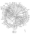
本発明の実施の形態の成膜装置の一例について、図1〜図9を参照して説明する。この装置は、図1〜図4に示すように、平面形状が概ね円形である真空容器1と、この真空容器1内に設けられ、平面で見た時に当該真空容器1の中心に回転中心を有する石英などからなる回転テーブル2と、を備えており、シリコン(Si)からなるウエハWに対して薄膜の成膜処理を行うように構成されている。そして、この成膜装置は、後で詳述するように、ウエハWの表面に例えば数十から百を超えるアスペクト比を持つ凹部が形成されていても、当該凹部の深さ方向に亘って緻密で且つ均質な薄膜を形成できるように構成されている。続いて、この成膜装置の各部について以下に説明する。
An example of a film forming apparatus according to an embodiment of the present invention will be described with reference to FIGS. As shown in FIGS. 1 to 4, this apparatus is provided with a vacuum container 1 having a substantially circular planar shape, and a center of rotation at the center of the vacuum container 1 when viewed in a plane. And a
真空容器1は、天板11及び容器本体12を備えており、天板11が容器本体12から着脱できるように構成されている。天板11の上面側における中央部には、真空容器1内の中心部領域Cにおいて互いに異なる処理ガス同士が混ざり合うことを抑制するために、窒素(N2)ガスを分離ガスとして供給するための分離ガス供給管51が接続されている。図1中13は、容器本体12の上面の周縁部にリング状に設けられたシール部材例えばOリングである。また、図2中10aは、後述の搬送口15を介して真空容器1内に搬入される搬送アーム10b上のウエハWを検出するためのカメラユニットである。また、各図では記載を省略しているが、このカメラユニット10aに対して周方向に離間した位置における天板11上には、当該天板11に嵌め込まれた透明窓などを介して回転テーブル2上のウエハWの温度を検出するための例えば放射温度計などからなる温度検出部が設けられている。
The vacuum container 1 includes a
回転テーブル2は、中心部にて概略円筒形状のコア部21に固定されており、このコア部21の下面に接続されると共に鉛直方向に伸びる回転軸22によって、鉛直軸周りこの例では時計周りに回転自在に構成されている。図1中23は回転軸22を鉛直軸周りに回転させる駆動部(回転機構)であり、20は回転軸22及び駆動部23を収納するケース体である。このケース体20は、上面側のフランジ部分が真空容器1の底面部14の下面に気密に取り付けられている。また、このケース体20には、回転テーブル2の下方領域に窒素ガスをパージガスとして供給するためのパージガス供給管72が接続されている。真空容器1の底面部14におけるコア部21の外周側は、回転テーブル2に下方側から近接するようにリング状に形成されて突出部12aをなしている。
The rotary table 2 is fixed to a substantially
真空容器1の底面部14の上方側には、図1に示すように、加熱部であるヒータユニット7が設けられており、回転テーブル2を介して回転テーブル2上のウエハWを成膜温度例えば300℃〜650℃に加熱するように構成されている。図1中71aはヒータユニット7の側方側に設けられたカバー部材、7aはこのヒータユニット7の上方側を覆う覆い部材である。また、底面部14には、ヒータユニット7の下方側において、ヒータユニット7の配置空間をパージするためのパージガス供給管73が周方向に亘って複数箇所に設けられている。
As shown in FIG. 1, a
回転テーブル2の表面部には、図3〜図4に示すように、ウエハWを落とし込んで保持するために、円形の凹部24が基板載置領域として設けられており、この凹部24は、当該回転テーブル2の回転方向(周方向)に沿って複数箇所例えば5箇所に形成されている。凹部24の通過領域と各々対向する位置には、各々例えば石英からなる5本のノズル31、32、34、41、42が真空容器1の周方向に互いに間隔をおいて放射状に配置されている。これら各ノズル31、32、34、41、42は、例えば真空容器1の外周壁から中心部領域Cに向かってウエハWに対向して水平に伸びるように各々取り付けられている。この例では、後述の搬送口15から見て時計周り(回転テーブル2の回転方向)にプラズマ発生用ガスノズル34、分離ガスノズル41、第1の処理ガスノズル31、分離ガスノズル42及び第2の処理ガスノズル32がこの順番で配列されている。
As shown in FIGS. 3 to 4, a
処理ガスノズル31、32は、夫々第1の処理ガス供給部及び第2の処理ガス供給部をなし、プラズマ発生用ガスノズル34はプラズマ発生用ガス供給部をなしている。また、分離ガスノズル41、42は、各々分離ガス供給部をなしている。尚、図3及び図4はノズル34、42が見えるように後述のプラズマ処理部80、筐体90及び加熱ランプ120を取り外した状態、図4はこれらプラズマ処理部80、筐体90及び加熱ランプ120を取り付けた状態を表している。
The
各ノズル31、32、34、41、42は、流量調整バルブを介して夫々以下の各ガス供給源(図示せず)に夫々接続されている。即ち、第1の処理ガスノズル31は、Si(シリコン)を含む第1の処理ガス例えばBTBAS(ビスターシャルブチルアミノシラン、SiH2(NH−C(CH3)3)2)ガスなどの供給源に接続されている。第2の処理ガスノズル32は、第2の処理ガス例えばオゾン(O3)ガスと酸素(O2)ガスとの混合ガスの供給源(詳しくはオゾナイザーの設けられた酸素ガス供給源)に接続されている。プラズマ発生用ガスノズル34は、例えばアルゴン(Ar)ガスと酸素ガスとの混合ガスからなるプラズマ発生用ガスの供給源に接続されている。分離ガスノズル41、42は、分離ガスである窒素ガスのガス供給源に各々接続されている。これらガスノズル31、32、34、41、42の例えば下面側には、ガス吐出孔33が各々形成されており、このガス吐出孔33は、回転テーブル2の半径方向に沿って複数箇所に例えば等間隔に配置されている。図3中31aは、第1の処理ガスノズル31の上方側に設けられたノズルカバーであり、当該ノズル31から吐出された処理ガスが回転テーブル2上のウエハWの表面に沿って通流するように構成されている。
Each
処理ガスノズル31、32の下方領域は、夫々第1の処理ガスをウエハWに吸着させるための第1の処理領域(成膜領域)P1及びウエハWに吸着した第1の処理ガスの成分と第2の処理ガスとを反応させるための第2の処理領域P2となる。プラズマ発生用ガスノズル34の下方側の領域は、ウエハWに対してプラズマ改質処理を行うための改質領域P3となる。即ち、プラズマ発生用ガスノズル34の上方側には、図1、図4及び図5に示すように、当該ノズル34から供給されるガスをプラズマ化するために、金属線からなるアンテナ83をコイル状に巻回して構成されたプラズマ処理部80が設けられている。尚、図2では、プラズマ処理部80については描画を省略している。
The lower regions of the
このアンテナ83は、図4に示すように、平面で見た時に回転テーブル2の中央部側から外周部側に亘ってウエハWの通過領域を跨ぐように配置されており、回転テーブル2の半径方向に沿って伸びる帯状の領域を囲むように概略8角形をなしている。また、このアンテナ83は、整合器84を介して周波数が例えば13.56MHz及び出力電力が例えば5000Wの高周波電源85に接続されると共に、真空容器1の内部領域から気密に区画されるように配置されている。
As shown in FIG. 4, the
即ち、プラズマ発生用ガスノズル34の上方側における天板11は、平面的に見た時に概略扇形に開口しており、例えば石英などからなる筐体90によって気密に塞がれている。この筐体90は、周縁部が周方向に亘ってフランジ状に水平に伸び出すと共に、中央部が真空容器1の内部領域に向かって窪むように形成されており、この筐体90の内側に前記アンテナ83が収納されている。図1中11aは、筐体90と天板11との間に設けられたシール部材であり、91は、筐体90の周縁部を下方側に向かって押圧するための押圧部材である。また図1中86は、プラズマ処理部80と整合器84及び高周波電源85とを電気的に接続するための接続電極である。
That is, the
筐体90の下面は、当該筐体90の下方領域への窒素ガスやオゾンガスなどの侵入を阻止するために、図1及び図6に示すように、外縁部が周方向に亘って下方側(回転テーブル2側)に向かって垂直に伸び出して、ガス規制用の突起部92をなしている。そして、この突起部92の内周面、筐体90の下面及び回転テーブル2の上面により囲まれた領域には、既述のプラズマ発生用ガスノズル34が収納されている。
As shown in FIGS. 1 and 6, the lower surface of the
筐体90とアンテナ83との間には、図1、図4及び図5に示すように、上面側が開口する概略箱型のファラデーシールド95が配置されており、このファラデーシールド95は、導電性の板状体である金属板により構成されると共に接地されている。このファラデーシールド95の底面には、アンテナ83において発生する電界及び磁界(電磁界)のうち電界成分が下方のウエハWに向かうことを阻止すると共に、磁界をウエハWに到達させるために、スリット97が形成されている。このスリット97は、アンテナ83の巻回方向に対して直交する方向に伸びるように形成されており、アンテナ83に沿うように周方向に亘って当該アンテナ83の下方位置に設けられている。ファラデーシールド95とアンテナ83との間には、これらファラデーシールド95とアンテナ83との絶縁を取るために、例えば石英からなる絶縁板94が介在している。尚、図4ではスリット97について省略している。
As shown in FIGS. 1, 4, and 5, an approximately box-shaped
分離ガスノズル41、42は、各々第1の処理領域P1と第2の処理領域P2とを分離する分離領域Dを各々形成するためのものである。これら分離ガスノズル41、42のうち、始めに分離ガスノズル41について説明すると、当該分離ガスノズル41の上方側における天板11には、図3及び図4に示すように、概略扇形の凸状部4が設けられている。そして、分離ガスノズル41は、この凸状部4の下面において回転テーブル2の半径方向に沿うように形成された溝部43内に収められている。従って、分離ガスノズル41における回転テーブル2の周方向両側には、図8に示すように、各処理ガス同士の混合を阻止するために、前記凸状部4の下面である低い天井面44が配置され、この天井面44の前記周方向両側には、当該天井面よりも高い天井面45が配置されている。凸状部4の周縁部(真空容器1の外縁側の部位)は、各処理ガス同士の混合を阻止するために、回転テーブル2の外端面に対向すると共に容器本体12に対して僅かに離間するように、下方側に向かって直角に屈曲している。尚、図8ではプラズマ処理部80を簡略化して描画している。
The
続いて、分離ガスノズル42について説明する。この分離ガスノズル42の上方側には、既述のプラズマ処理部80にて説明した筐体90が設けられている。即ち、分離ガスノズル42の上方側における天板11は、平面で見た時に概略扇状に開口しており、筐体90により気密に塞がれている。そして、この筐体90についても、下面側における外縁部が周方向に亘って回転テーブル2に向かって垂直に伸び出して、ガス規制用の突起部92をなしている。従って、分離ガスノズル42から見ると、回転テーブル2の回転方向上流側及び下流側と、中心部領域C側と、回転テーブル2の外縁側とには突起部92が各々配置されている。そのため、この分離ガスノズル42から分離ガスを吐出すると、筐体90の下方側の領域が真空容器1内の他の領域よりも陽圧になり、回転テーブル2の回転方向上流側から第1の処理ガスが侵入すること、及び回転テーブル2の回転方向下流側から第2の処理ガスが侵入することが防止される。
Next, the
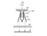
分離ガスノズル42から見て筐体90の上方側には、ウエハWに対して改質(熱アニール)処理を行うための加熱ランプ120が加熱機構として設けられている。この加熱ランプ120は、石英からなる部材(筐体90及び回転テーブル2)を透過すると共にウエハWが吸収する波長の光(例えば0.5μm〜3μmの赤外線)を当該ウエハWに照射して、既述の成膜温度よりも高いアニール温度例えば650℃〜900℃にウエハWを加熱するためのものであり、複数箇所に設けられている。即ち、回転テーブル2上においてウエハWが公転しており、回転テーブル2の回転中心側と外縁側とではウエハWの周速度が異なるので、回転テーブル2の半径方向においてウエハWの加熱温度を揃えるために、加熱ランプ120の配置個数及びレイアウトを調整している。具体的には、加熱ランプ120は、回転テーブル2の回転方向に沿って円弧状に複数箇所に配置されると共に、この円弧状の並びが回転テーブル2の半径方向に互いに離間するように同心円状に複数周この例では5周に亘って並べられている。
A
ここで、前記円弧状の並びを「ランプ群」と呼ぶと共に、各々のランプ群について、図4に示すように、回転テーブル2の回転中心側から外周側に向かって夫々「121」、「122」、「123」、「124」及び「125」の符号を付すと、これらランプ群121〜125における各々の加熱ランプ120は、回転テーブル2の回転中心側から外周部側に向かって数量が増えるように配置されており、具体的には夫々2個、3個、4個、5個及び6個となっている。また、回転テーブル2の回転中心側のランプ群121は、回転テーブル2上のウエハWにおける当該回転中心側の外縁の上方側に位置するように配置されている。回転テーブル2の外周側のランプ群125は、回転テーブル2上のウエハWにおける当該外周側の外縁の上方側に位置するように配置されている。そして、ランプ群122〜124は、回転中心側のランプ群121と、外周側のランプ群125と、の間において回転テーブル2の半径方向に互いに等間隔となるように配置されている。
Here, the arc-shaped arrangement is referred to as a “lamp group”, and for each lamp group, as shown in FIG. 4, “121”, “122” respectively from the rotation center side to the outer periphery side of the
各々の加熱ランプ120について簡単に説明すると、これら加熱ランプ120は、図7に示すように、概略円筒状に上下方向に伸びるガラスなどの光透過材131の内部に輻射源をなす光源132が封入されてハロゲンランプとして各々構成されている。そして、光源132から上方側及び側方側に照射される赤外線を下方側に反射させるために、光透過材131の上方側及び側周面を覆うように、下方側が開口する概略円錐形状の反射部材133が設けられている。従って、光源132から輻射熱として照射される赤外線は、下方側に向かって集約されると共に、光透過材131、筐体90を透過して、回転テーブル2上のウエハWに吸収される。そして、回転テーブル2が既述のように石英により構成されていることから、加熱ランプ120は、ウエハWのみを輻射熱により局所的に加熱することとなる。こうして分離ガスノズル42の下方側の領域は、既述のように分離領域Dをなすと共に、回転テーブル2上のウエハWに対してアニール処理を行う加熱領域P4をなしている。
Each
図7中134は各々の加熱ランプ120に給電するための電源部であり、ウエハWを面内に亘って均一な温度に加熱するために、給電量を例えば300W以下の範囲にて各々のランプ群121〜125毎に調整できるように構成されている。また、図1中135は、下面側が開口する概略箱型の収納部材であり、各々の加熱ランプ120は、この収納部材135の内部において上端部が支持されて、赤外線の照射位置が各々の加熱ランプ120にて揃うように構成されている。尚、図1では、一部の反射部材133については縦断面を示しており、また図5では加熱ランプ120や当該加熱ランプ120の下方側の筐体90について省略している。
In FIG. 7,
図9は、以上説明した各ガスが供給される領域を模式的に示したものであり、第1の処理ガス及び第2の処理ガスが夫々供給される処理領域P1、P2間には各々分離ガスが供給される分離領域Dが介在している。そして、処理領域P2の下流側の分離領域Dと当該処理領域P2との間には、改質領域P3が位置すると共に、この分離領域Dに対して回転テーブル2の周方向に離間して配置された別の分離領域Dは、既述のように加熱領域P4をなしている。
FIG. 9 schematically shows the regions to which the respective gases described above are supplied, and separation is made between the processing regions P1 and P2 to which the first processing gas and the second processing gas are supplied, respectively. A separation region D to which gas is supplied is interposed. A reforming region P3 is located between the separation region D on the downstream side of the processing region P2 and the processing region P2, and is arranged away from the separation region D in the circumferential direction of the
回転テーブル2の外周側において当該回転テーブル2よりも僅かに下位置には、リング状のサイドリング100が配置されており、このサイドリング100の上面には、互いに周方向に離間するように2箇所に排気口61、62が形成されている。言い換えると、真空容器1の底面部14に2つの排気口が形成され、これら排気口に対応する位置におけるサイドリング100に、排気口61、62が形成されている。これら2つの排気口61、62のうち一方及び他方を夫々第1の排気口61及び第2の排気口62と呼ぶと、第1の排気口61は、第1の処理ガスノズル31と、当該第1の処理ガスノズル31よりも回転テーブルの回転方向下流側における分離領域Dとの間において、当該分離領域D側に寄った位置に形成されている。第2の排気口62は、プラズマ発生用ガスノズル34と、当該プラズマ発生用ガスノズル34よりも回転テーブルの回転方向下流側における分離領域Dとの間において、当該分離領域D側に寄った位置に形成されている。
A ring-shaped
第1の排気口61は、第1の処理ガス及び分離ガスを排気するためのものであり、第2の排気口62は、第2の処理ガス及び分離ガスに加えて、プラズマ発生用ガスを排気するためのものである。そして、2つの筐体90、90のうちプラズマ発生用ガスノズル34の上方側の筐体90について、当該筐体90の外縁側におけるサイドリング100の上面に、この筐体90を避けてガスを第2の排気口62に通流させるための溝状のガス流路101が形成されている。これら第1の排気口61及び第2の排気口62は、図1に示すように、各々バタフライバルブなどの圧力調整部65の介設された排気管63により、真空排気機構である例えば真空ポンプ64に接続されている。
The
天板11の下面における中央部には、図3などに示すように、凸状部4における中心部領域C側の部位と連続して周方向に亘って概略リング状に形成されると共に、その下面が凸状部4の下面と同じ高さに形成された突出部5が設けられている。この突出部5よりも回転テーブル2の回転中心側におけるコア部21の上方側には、中心部領域Cにおいて第1の処理ガスと第2の処理ガスとが互いに混ざり合うことを抑制するためのラビリンス構造部110が配置されている。このラビリンス構造部110は、回転テーブル2側から天板11側に向かって周方向に亘って垂直に伸びる第1の壁部111と、天板11側から回転テーブル2に向かって周方向に亘って垂直に伸びる第2の壁部112と、を回転テーブル2の半径方向に交互に配置した構成を採っている。
As shown in FIG. 3 and the like, the central portion of the lower surface of the
真空容器1の側壁には、図2〜図4に示すように、外部の搬送アーム10bと回転テーブル2との間においてウエハWの受け渡しを行うための搬送口15が形成されており、この搬送口15はゲートバルブGより気密に開閉自在に構成されている。また、この搬送口15を臨む位置における回転テーブル2の下方側には、回転テーブル2の貫通口を介してウエハWを裏面側から持ち上げるための昇降ピン(いずれも図示せず)が設けられている。
As shown in FIGS. 2 to 4, a
また、この成膜装置には、装置全体の動作のコントロールを行うためのコンピュータからなる制御部200が設けられており、この制御部200のメモリ内には後述の成膜処理、改質処理及びアニール処理を行うためのプログラムが格納されている。このプログラムは、後述の装置の動作を実行するようにステップ群が組まれており、ハードディスク、コンパクトディスク、光磁気ディスク、メモリカード、フレキシブルディスクなどの記憶媒体である記憶部201から制御部200内にインストールされる。
In addition, the film forming apparatus is provided with a
次に、上述実施の形態の作用について、図10〜図14及び図15のフローチャートに基づいて説明する。先ず、ゲートバルブGを開放して、回転テーブル2を間欠的に回転させながら、搬送アーム10bにより搬送口15を介して回転テーブル2上に例えば5枚のウエハWを載置する。各々のウエハWの表面には、図10に示すように、溝やホールなどからなる凹部10が形成されており、この凹部10のアスペクト比(凹部10の深さ寸法÷凹部10の幅寸法)は、例えば数十から百を超える大きさになっている。次いで、ゲートバルブGを閉じ、真空ポンプ64により真空容器1内を引き切りの状態にすると共に、回転テーブル2を例えば2rpm〜240rpmで時計周りに回転させる。そして、ヒータユニット7によりウエハWを例えば300℃程度に加熱する(ステップS11)。
Next, the operation of the above-described embodiment will be described based on the flowcharts of FIGS. 10 to 14 and 15. First, the gate valve G is opened, and, for example, five wafers W are placed on the rotary table 2 via the
続いて、処理ガスノズル31、32から夫々第1の処理ガス及び第2の処理ガスを吐出すると共に、プラズマ発生用ガスノズル34からプラズマ発生用ガスを吐出する。また、分離ガスノズル41、42から分離ガスを所定の流量で吐出し、分離ガス供給管51及びパージガス供給管72、72からも窒素ガスを所定の流量で吐出する。そして、圧力調整部65により真空容器1内を予め設定した処理圧力に調整する。
Subsequently, the first processing gas and the second processing gas are discharged from the
第1の処理領域P1では、図11に示すように、ウエハWの表面に第1の処理ガスの成分が吸着して吸着層300が生成する(ステップS12)。次いで、第2の処理領域P2において、図12に示すように、ウエハW上の吸着層300が酸化されて、薄膜成分であるシリコン酸化膜(SiO2)の分子層が1層あるいは複数層形成されて反応生成物である反応層301が形成される(ステップS13)。この反応層301には、例えば第1の処理ガスに含まれる残留基のため、水分(OH基)や有機物などの不純物が残る場合がある。
In the first processing region P1, as shown in FIG. 11, the component of the first processing gas is adsorbed on the surface of the wafer W to generate the adsorption layer 300 (step S12). Next, in the second processing region P2, as shown in FIG. 12, the
プラズマ処理部80では、高周波電源85から供給される高周波電力によって電界及び磁界が発生する。これら電界及び磁界のうち電界は、ファラデーシールド95により反射あるいは吸収(減衰)されて、真空容器1内への到達が阻害される。一方、磁界は、ファラデーシールド95にスリット97を形成しているので、このスリット97を通過して、筐体90の底面を介して真空容器1内の改質領域P3に到達する。
In the
従って、プラズマ発生用ガスノズル34から吐出されたプラズマ発生用ガスは、図13に示すように、磁界によって活性化されて、例えばイオン(アルゴンイオン:Ar+)やラジカルなどのプラズマが生成する。既述のように、回転テーブル2の半径方向に伸びる帯状体領域を囲むようにアンテナ83を配置していることから、このプラズマは、アンテナ83の下方側において、回転テーブル2の半径方向に伸びるように概略ライン状となる。このプラズマにウエハWが接触すると、反応層301の改質処理が行われることになる(ステップS14)。具体的には、プラズマがウエハWの表面に衝突することにより、反応層301から水分や有機物などの不純物が放出されたり、反応層301内の元素の再配列が起こって当該反応層301の緻密化(高密度化)が図られたりすることになる。
Therefore, as shown in FIG. 13, the plasma generating gas discharged from the plasma generating
こうして回転テーブル2の回転によって以上説明した吸着層300の成膜処理と、吸着層300の酸化による反応層301の形成処理と、反応層301のプラズマ改質処理と、を多数回(n回、n:自然数)に亘って繰り返すと、反応層301がn層に亘って積層されて薄膜が形成される。即ち、既述の制御部200では、吸着層300の形成、反応層301の形成及びプラズマ改質処理を行った後、回転テーブル2が既にn回回転したか否か、言い換えると反応層301の積層数がn層に到達したか否かを判断している(ステップS15)。反応層301がn層に達していない場合には、回転テーブル2の回転及び各ガスの供給や高周波電源85への給電を継続する。
Thus, the film forming process of the
ここで、ウエハWの表面には既述のように極めて大きなアスペクト比の凹部10が形成されているので、当該凹部10内にはプラズマが入り込みにくい。また、真空容器1内においてプラズマ改質処理と共に成膜処理を行っているので、この真空容器1内の処理圧力は、プラズマが良好に活性を保ちやすい圧力よりも高圧になっている。そのため、凹部10の底面に向かってプラズマが侵入していく時に、例えば凹部10の内壁面にプラズマが接触すると、このプラズマが失活してしまう。従って、図13に示すように、凹部10内では、底面に向かうにつれてプラズマ改質処理の度合いが小さくなるので、上方側から下方側に向かって膜厚が大きくなっていく膜厚勾配が形成される。言い換えると、ウエハWの表面(互いに隣接する凹部10、10間における水平面)では良好にプラズマ改質処理が行われて緻密な薄膜が形成される一方、凹部10の底面に向かうにつれて密度の低い(疎の)薄膜となる。そこで、凹部10の深さ方向に亘って緻密な薄膜を形成するために、既述のステップS15においてn層の反応層301が積層されていて薄膜の成膜が完成していると判断された場合には、以下のようにしてアニール処理による薄膜の改質処理を行う。
Here, since the
具体的には、各ガス(第1の処理ガス、第2の処理ガス、プラズマ発生用ガス、分離ガス)の供給を停止すると共に、高周波電源85への給電を停止する(ステップS16)。そして、真空容器1内からの各ガスの排気が終了した後、即ち真空容器1内の圧力を例えば133〜1333Pa(1〜10Torr)まで減圧した後、各加熱ランプ120に対して電源部134から各々給電する(加熱ランプ120をオンにする)と、これら加熱ランプ120から赤外線が下方側に向かって照射される。この赤外線は、既述のように筐体90及び回転テーブル2を透過する一方、ウエハWに吸収される。そのため、回転テーブル2によって公転している各々のウエハWは、局所的に且つ急速に既述のアニール温度に加熱される。従って、回転テーブル2などの真空容器1内の他の部材は、昇温が抑制される。
Specifically, the supply of each gas (the first processing gas, the second processing gas, the plasma generating gas, and the separation gas) is stopped and the power supply to the high-
こうして回転テーブル2が回転している間に各々のウエハWが加熱ランプ120によって例えば5秒〜120秒の間に亘って加熱されると、ウエハWの厚さ方向に亘って既述のアニール温度となるので、図14に示すように、凹部10の内部にて薄膜内に残っていた既述の水分などの不純物は、当該薄膜から除去されて、凹部10の深さ方向に亘って均質で緻密な薄膜が得られる(ステップS17)。従って、薄膜の膜厚についても、凹部10の深さ方向に亘って均一になる。以上のアニール処理を行っている間、回転テーブル2とウエハWとが接触してので、当該ウエハWからの入熱によって回転テーブル2が昇温していく。しかしながら、回転テーブル2を赤外線に対して透明な石英により構成しているので、またアニール処理が既述のように短時間で終了するので、回転テーブル2の昇温量は極僅かである。尚、以上説明した図11〜図14において、凹部10の寸法や各膜(吸着層300、反応層301)の寸法について模式的に描画している。
When each wafer W is heated by the
また、以上の一連のプロセスを行っている間、サイドリング100にガス流路101を形成しているので、各ガスは、このガス流路101の上方側の筐体90を避けるように、当該ガス流路101を通って排気される。更に、各々の筐体90の下端側周縁部に突起部92を設けていることから、各筐体90内への窒素ガスや各処理ガスの侵入が抑えられる。
Moreover, since the
更にまた、第1の処理領域P1と第2の処理領域P2との間に窒素ガスを供給しているので、第1の処理ガスと第2の処理ガス及びプラズマ発生用ガスとが互いに混合しないように各ガスが排気される。また、回転テーブル2の下方側にパージガスを供給しているため、回転テーブル2の下方側に拡散しようとするガスは、前記パージガスにより排気口61、62側へと押し戻される。
Furthermore, since nitrogen gas is supplied between the first processing region P1 and the second processing region P2, the first processing gas, the second processing gas, and the plasma generating gas do not mix with each other. Each gas is exhausted. Further, since the purge gas is supplied to the lower side of the
上述の実施の形態によれば、回転テーブル2を回転させながら、反応層301を形成するステップと、この反応層301をプラズマにより改質するステップとを繰り返して薄膜を形成した後、各ガスの供給を停止すると共に、薄膜形成時の温度よりも高い温度にウエハWを加熱して薄膜を改質している。そのため、ウエハWの表面に既述のようにアスペクト比の大きな凹部10が形成されていても、当該凹部10の深さ方向に亘って均質で緻密な(良質な)薄膜を形成できる。
According to the above-described embodiment, after forming the thin film by repeating the step of forming the
ここで、プラズマ改質処理と共にアニール処理を以上説明したシーケンスで行っている理由について詳述する。後述の実施例に示すように、例えば300℃程度あるいは650℃程度の低温の成膜温度にてALD法を用いてシリコン酸化膜からなる薄膜を成膜しただけだと、当該薄膜は、熱酸化膜(シリコン基板を加熱しながら酸化処理して得られた酸化膜)と比べて、フッ酸(フッ化水素水溶液)に対するエッチングレートが速い。従って、ALD法により成膜したシリコン酸化膜は、熱酸化膜よりも膜密度が低いと言える。このような薄膜の膜密度を向上させる技術として、背景の項目で述べたように、プラズマ改質処理が知られている。そして、反応層301を形成する度に当該反応層301を改質することにより、即ち各処理領域P1、P2に対して周方向に離間した位置にプラズマ処理部80を配置することにより、既述のように低温で成膜した薄膜であっても良好な膜密度が得られる。しかしながら、ウエハWの表面に凹部10が形成されていると、当該凹部10の底面付近まではプラズマが到達しにくいので、凹部10の深さ方向において膜密度がばらついてしまう。
Here, the reason why the annealing process and the annealing process are performed in the sequence described above will be described in detail. As shown in the examples described later, for example, when a thin film made of a silicon oxide film is formed by using the ALD method at a low film forming temperature of about 300 ° C. or about 650 ° C., the thin film is thermally oxidized. Compared with a film (an oxide film obtained by oxidizing a silicon substrate while heating it), the etching rate for hydrofluoric acid (aqueous hydrogen fluoride solution) is faster. Therefore, it can be said that the silicon oxide film formed by the ALD method has a lower film density than the thermal oxide film. As a technique for improving the film density of such a thin film, as described in the background item, a plasma reforming process is known. By modifying the
一方、プラズマ改質処理と同様に薄膜の膜密度を向上させる技術として、成膜温度よりも高温においてウエハWを加熱する手法であるアニール処理が知られている。このようなアニール処理であれば、ウエハWの厚さ方向に亘って当該ウエハWを加熱できるので、既述のように凹部10が形成されていても、当該凹部10の深さ方向に亘って均一に熱処理を行うことができる。しかしながら、後述の実施例に示すように、アニール処理だけでは十分な膜密度が得られない。
On the other hand, an annealing process, which is a technique for heating the wafer W at a temperature higher than the film forming temperature, is known as a technique for improving the film density of a thin film as in the plasma modification process. With such an annealing process, since the wafer W can be heated in the thickness direction of the wafer W, even if the
そこで、本発明では、既に詳述したように、回転テーブル2が回転する度にプラズマ改質処理を行うと共に、反応層301を多層に亘って積層して薄膜を形成した後、アニール処理を行っている。即ち、プラズマ改質処理については反応層301を形成する度に行う一方、アニール処理については薄膜の形成後に一括して行う手法を採っている。従って、アニール処理をプラズマ改質処理と組み合わせて行うにあたって、本発明の手法は、得られる薄膜の膜質において、また装置の耐熱構造上において、更にはスループットの観点からも、極めて有効な手法である。即ち、薄膜の膜質としては、後述の実施例から分かるように、反応層301を形成する度にアニール処理を行わなくても、薄膜の形成後に一括してアニール処理を行うだけで十分に良質な膜質が得られる。そのため、加熱ランプ120に対して常時通電せずに済むので、コスト面からも有利である。
Therefore, in the present invention, as already described in detail, the plasma reforming process is performed each time the
また、装置の耐熱構造については、既述のように薄膜の形成後に一括してアニール処理を行うと共に、加熱ランプ120によってウエハWを局所的に加熱しているので、アニール処理に要する時間(加熱ランプ120に通電している時間)が数十秒程度の短時間で済む。そのため、このような短時間のアニール処理では、真空容器1内の回転テーブル2などの部材は、ウエハWと比べてほとんど昇温しない。従って、真空容器1と天板11及び筐体90とのシール構造や、回転テーブル2をコア部21に固定する部位における耐熱構造などについて、成膜処理を行う成膜温度(例えば300℃〜650℃)に耐えうる程度の耐熱構造で済む。即ち、装置について、アニール温度に耐える程度までの耐熱構造を取らなくても、言い換えるとアニール温度に耐えられない耐熱構造の装置であっても、アニール温度もの高温のアニール処理を行うことができる。
As for the heat-resistant structure of the apparatus, as described above, the annealing process is collectively performed after the formation of the thin film, and the wafer W is locally heated by the
従って、装置メーカー側からすると、成膜処理やプラズマ改質だけを行う装置と、既述のようにこれら処理に加えてアニール処理を行う装置とにおいて、加熱ランプ120や天板11(筐体90)の構成以外の部材(ヒータユニット7の加熱機構など)については共用化できる。即ち、ALD法を用いた成膜処理とプラズマ改質処理とを行う装置を構成しておけば、加熱ランプ120や筐体90を設けるだけで高温のアニール処理を行うことができる。従って、装置の汎用性が高くなり、当該装置を製造するにあたってコストダウンを図ることができると言える。
Therefore, from the viewpoint of the apparatus manufacturer, the
このような装置を用いて成膜されるシリコン酸化膜の適用例について一例を挙げると、ウエハWをエッチングするためのハードマスクとしてシリコン酸化膜を成膜する時には、当該シリコン酸化膜はその後除去されるので、緻密さについてそれ程要求レベルは高くない。従って、このような場合には、加熱ランプ120を設けない装置が用いられる。一方、例えば凹部内にその後埋め込まれる銅配線に対するバリア膜としてシリコン酸化膜を当該凹部の内壁面に沿って形成する時には、当該シリコン酸化膜は、デバイスの形成後も残るので、このシリコン酸化膜についてはできるだけ緻密であることが求められる。従って、この場合には、加熱ランプ120を備えた装置が用いられる。このように、シリコン酸化膜が適用されるデバイスに応じて、即ちシリコン酸化膜の緻密さについての要求レベルに応じて、適用される装置が選択される。
As an example of an application example of a silicon oxide film formed using such an apparatus, when a silicon oxide film is formed as a hard mask for etching the wafer W, the silicon oxide film is subsequently removed. Therefore, the required level of precision is not so high. Therefore, in such a case, an apparatus without the
そして、一つの共通の真空容器1に各ノズル31、32、41、42及びプラズマ処理部80に加えて加熱ランプ120を組み込むことにより、いわばin situ (イン・サイチュ)でアニール処理を行うことができる。そのため、例えば成膜処理及びプラズマ改質処理を行った後、別の熱処理装置にて熱処理を行う場合と比べて、真空容器1から前記別の熱処理装置へのウエハWの搬送が不要になるので、ウエハWの搬送に要する時間の分だけスループットの向上を図ることができる。
Then, by incorporating the
また、アニール処理を真空容器1内にて行うにあたって、アニール処理におけるウエハWの加熱温度は、既述のように650℃〜900℃と成膜時の温度よりも高い。更に、このアニール温度は、第1の処理ガスであるBTBASガスの熱分解温度(例えば550℃)や、第2の処理ガスであるオゾンの熱分解温度(例えば600℃)よりも高い。そして、加熱ランプ120にてアニール温度に加熱されたウエハWは、後段側の第1の処理領域P1や第2の処理領域P2に到達しても、回転テーブル2が高速で回転しているので、それ程降温していない。そのため、各ガスを供給しながらアニール処理を行おうとすると、このような高温のウエハWに各処理ガスが接触した時、各ガスが熱分解して、第1の処理ガスの吸着や、吸着層300の酸化が良好に行われなくなってしまう。そこで、本発明では、アニール処理を行うにあたって、各ガスの供給を停止すると共に、真空容器1内からこれらガスを排気した上で、アニール処理を行っている。従って、各処理ガスの熱分解を抑制しながら、良好にアニール処理を行うことができる。また、アニール処理でも熱分解しない第2の処理ガスとして例えば酸素プラズマを得るためには、高周波電源などの付帯設備が必要になるが、この第2の処理ガスとしてオゾンガスを用いることにより、このような付帯設備更には当該付帯設備を駆動させる電力が不要になる。
Further, when the annealing process is performed in the vacuum vessel 1, the heating temperature of the wafer W in the annealing process is 650 ° C. to 900 ° C., which is higher than the temperature at the time of film formation as described above. Further, the annealing temperature is higher than the thermal decomposition temperature (for example, 550 ° C.) of the BTBAS gas that is the first processing gas and the thermal decomposition temperature (for example, 600 ° C.) of the ozone that is the second processing gas. Since the wafer W heated to the annealing temperature by the
そして、加熱ランプ120について、第1の処理領域P1と第2の処理領域P2とを分離するための分離領域Dの上方側に配置して、いわばこの分離領域Dとアニール処理を行うための加熱領域P4とを兼用させている。そのため、天板11上にはプラズマ処理部80、カメラユニット10a及びウエハWの温度検出部が周方向に配置されていて、真空容器1内には各ガスノズル31、32、34、41、42が周方向に配置されている、空きスペースのほとんどない既述の装置であっても、当該装置の大型化を抑えながらアニール処理を行うことができる。
加熱ランプ120については、分離ガスノズル41の上方側などに設けても良い。
Then, the
The
以上の例では、n層の反応層301を積層して薄膜を形成した後アニール処理を行ったが、薄膜の形成後におけるアニール処理に加えて、この薄膜の成膜途中においてアニール処理を行っても良い。具体的には、図16に示すように、既述の例と同様にしてm層(m:nよりも小さく且つ1以上の自然数)の反応層301を形成すると共に各々の反応層301のプラズマ改質処理を行った(ステップS21)後、各ガスの供給及び高周波電源85への給電を停止する(ステップS22)。次いで、加熱ランプ120を用いて、m層の反応層301のアニール処理を行う(ステップS23)。続いて、反応層301の積層数がn層に到達していない場合(ステップS24)には、第1の処理ガス、第2の処理ガス及びプラズマ発生用ガスについては供給を停止したまま、例えば分離ガスを真空容器1内に供給して、ヒータユニット7による成膜温度となるまでウエハWを冷却する(ステップS25)。そして、再度プラズマ改質処理を行いながらm層の反応層301を積層した後、同様に各ガスを停止してアニール処理を行う。こうして反応層301の積層、アニール処理及びウエハWの冷却を繰り返すことにより、既述の例と同様にn層の反応層301が積層される。このようなシーケンスにおいても、既述の例と同様の効果が得られる。図16において、ステップS21〜S23からなるシーケンスを複数回に亘って繰り返すにあたり、ステップS21における反応層301の積層数mとしては、あるシーケンスと他のシーケンスとで互いに異なる値にしても良い。また、前記積層数mについて、1回でも良く、即ち反応層301を形成する度にアニール処理を行っても良い。尚、図16におけるステップS21は、既述の図15におけるステップS11〜S15に相当する。
In the above example, the n-
以上の各例において、アニール処理を行う時間(加熱ランプ120に通電する時間)は、短すぎるとウエハWの熱処理が不十分になり、長すぎるとウエハWからの入熱により回転テーブル2が昇温しすぎてしまい、装置の耐熱構造にダメージを与えるおそれがあることから、5秒〜120秒であることが好ましい。更に、加熱ランプ120に給電する時、各ガスの供給を停止して真空容器1内を真空排気したが、アニール処理を行う時点における真空容器1内の真空度は、高すぎると真空容器1内にまだ処理ガスが残留しているおそれがあり、一方低すぎるとスループットの低下に繋がってしまうことから、133〜1333Pa(1〜10Torr)程度であることが好ましい。尚、アニール処理を行う前に、真空容器1内の真空排気と当該真空容器1内への分離ガスの供給とを行って雰囲気の置換を行って、前記真空度以上の圧力においてアニール処理を行っても良い。
In each of the above examples, if the time for performing the annealing process (the time for energizing the heating lamp 120) is too short, the heat treatment of the wafer W is insufficient, and if it is too long, the
更に、プラズマ改質処理について、複数層例えば10〜100層の反応層301を形成する度に行っても良い。具体的には、成膜開始時には高周波電源85への給電を停止しておき、回転テーブル2を反応層301の積層数分だけ回転させた後、ノズル31、32へのガスの供給を停止すると共に、高周波電源85に対して給電してプラズマ改質を行う。その後、再度反応層301の積層とプラズマ改質とを繰り返す。また、本発明は、既述の凹部10が形成されているウエハWだけでなく、このような凹部10が形成されていない平坦なウエハWに対して適用しても良い。
Further, the plasma modification treatment may be performed each time a plurality of layers, for example, 10 to 100 reaction layers 301 are formed. Specifically, power supply to the high-
更にまた、以上述べた各例では、プラズマ処理部80としてアンテナ83を巻回して誘導結合型のプラズマ(ICP:Inductively coupled plasma)を発生させたが、容量結合型のプラズマ(CCP:Capacitively Coupled Plasma)を発生させるようにしても良い。この場合には、プラズマ発生用ガスノズル34に対して回転テーブル2の回転方向下流側に、図示しない一対の電極を平行電極として配置する。そして、これら電極間においてプラズマ発生用ガスをプラズマ化する。
Furthermore, in each of the examples described above, the
また、真空容器1内にて成膜処理及びプラズマ改質処理に加えてアニール処理についても行ったが、アニール処理については別の熱処理装置(加熱機構)にて行っても良い。具体的には、多数枚例えば100枚程度のウエハWを棚状に保持するウエハボートと、このウエハボートを下方側から気密に収納する反応管とを備えた縦型熱処理装置を用いて、成膜処理及びプラズマ改質処理が終了した処理済みのウエハWを一括してアニールするようにしても良い。 In addition to the film forming process and the plasma reforming process in the vacuum vessel 1, the annealing process is also performed. However, the annealing process may be performed by another heat treatment apparatus (heating mechanism). Specifically, a vertical heat treatment apparatus including a wafer boat that holds a large number of, for example, about 100 wafers W in a shelf shape, and a reaction tube that hermetically stores the wafer boat from below is formed. The processed wafers W that have been subjected to the film processing and plasma modification processing may be annealed together.
以上説明したシリコン酸化膜を成膜するにあたって用いる第1の処理ガスとしては、以下の表1の化合物を用いても良い。尚、以下の各表において、「原料Aエリア」とは、第1の処理領域P1を示しており、「原料Bエリア」とは、第2の処理領域P2を示している。また、以下の各ガスは一例であり、既に説明したガスについても併せて記載している。 As the first processing gas used for forming the silicon oxide film described above, the compounds shown in Table 1 below may be used. In the following tables, “raw material A area” indicates the first processing region P1, and “raw material B area” indicates the second processing region P2. Further, the following gases are examples, and the gases already described are also described.
(表1)

第1の処理ガスとして3DMASあるいは4DMASを用いると、この第1の処理ガスの熱分解温度は、BTBASの熱分解温度よりも高くなり、またアニール温度よりも高くなる。
また、表1の第1の処理ガスを酸化するための第2の処理ガスとしては、表2の化合物を用いても良い。
尚、この表2における「プラズマ+O2」や「プラズマ+O3」とは、例えば第2の処理ガスノズル32の上方側にプラズマ処理部80を設けて、あるいは既述の平行電極を用いて、これら酸素ガスやオゾンガスをプラズマ化して用いることを意味している。第2の処理ガスとして酸素ガスのプラズマを用いた場合には、当該第2の処理ガスの熱分解温度は、既述のオゾンガスの熱分解温度よりも高くなり、アニール温度以上となる。
When 3DMAS or 4DMAS is used as the first processing gas, the thermal decomposition temperature of the first processing gas is higher than the thermal decomposition temperature of BTBAS and higher than the annealing temperature.
Further, as the second processing gas for oxidizing the first processing gas in Table 1, the compounds in Table 2 may be used.
Note that “plasma +
また、既述の表1の化合物を第1の処理ガスとして用いると共に、表3の化合物からなるガスを第2の処理ガスとして用いて、シリコン窒化膜(SiN膜)を形成しても良い。
(表3)
(Table 3)
更に、第1の処理ガス及び第2の処理ガスとして表4の化合物からなるガスを各々用いて、炭化シリコン(SiC)膜を成膜しても良い。
(表4)
(Table 4)
更にまた、上に挙げた表4の第1の処理ガスを用いて、シリコン膜(Si膜)を成膜しても良い。即ち、この場合には第2の処理ガスノズル32が設けられておらず、回転テーブル2上のウエハWは、第1の処理領域(成膜領域)P1と改質領域P3とを分離領域Dを介して交互に通過することになる。そして、第1の処理領域P1においてウエハWの表面に第1の処理ガスの成分が吸着して吸着層300が形成されると、回転テーブル2によって回転する間に、ヒータユニット7の熱によってウエハWの表面にて吸着層300が熱分解を起こして水素や塩素などの不純物が脱離していく。従って、吸着層300の熱分解反応によって反応層301が形成されていく。
Furthermore, a silicon film (Si film) may be formed using the first processing gas shown in Table 4 above. That is, in this case, the second
しかしながら、回転テーブル2が鉛直軸周りに回転していることから、回転テーブル2上のウエハWが第1の処理領域P1を通過した後、改質領域P3に至るまでの時間、即ち吸着層300から不純物を排出するための時間は極めて短い。そのため、改質領域P3に到達する直前のウエハWの反応層301には、依然として不純物が含まれている。そこで、改質領域P3において例えばアルゴンガスのプラズマをウエハWに供給することにより、反応層301から不純物が除去されて、良好な膜質の反応層301が得られる。こうして領域P1、P3を交互に通過させることにより、反応層301が多層積層されてシリコン膜が成膜される。その後、処理ガスの供給を停止してアニール処理を行うことにより、凹部10の深さ方向に亘って均一で良質な薄膜が得られる。従って、本発明において「プラズマ改質処理」とは、反応層301から不純物を除去して当該反応層301の改質を行う処理の他に、吸着層300を反応(熱分解反応)させるための処理も含まれる。
シリコン膜のプラズマ処理に用いるプラズマ発生用ガスとしては、ウエハWに対してイオンのエネルギーを与えるプラズマを発生させるガスが用いられ、具体的には既述のアルゴンガスの他に、ヘリウム(He)ガスなどの希ガスあるいは水素ガスなどが用いられる。
However, since the
As the plasma generating gas used for plasma processing of the silicon film, a gas for generating plasma that gives ion energy to the wafer W is used. Specifically, in addition to the above-described argon gas, helium (He) is used. A rare gas such as gas or hydrogen gas is used.
また、シリコン膜を形成する場合には、第2の処理ガスとして表5のドープ材を用いて、ホウ素(B)やリン(P)を当該シリコン膜にドープしても良い。
(表5)
(Table 5)
また、以下の表6に示す化合物からなるガスを第1の処理ガスとして用いると共に、既述の第2の処理ガスを用いることにより、金属酸化膜、金属窒化膜、金属炭化膜あるいはHigh−k膜(高誘電率膜)を形成しても良い。
(表6)
(Table 6)
また、プラズマ改質用ガスあるいは当該プラズマ改質用ガスと共に用いるプラズマイオン注入ガスとしては、以下の表7の化合物からなるガスのプラズマを用いても良い。
(表7)
以上述べた各種の薄膜を成膜する時においても、薄膜の形成後にアニール処理を行っても良いし、薄膜の成膜途中あるいは反応層301を形成する度にアニール処理を行っても良い。また、アニール処理を行う時、各ガスの供給及び高周波電源85への給電を停止したが、分離ガス及びプラズマ発生用ガスの供給、更には高周波電源85への給電(プラズマ発生用ガスのプラズマ化)については、アニール処理に特に悪影響を及ぼさないことから、当該アニール処理を行っている時に前記供給や給電を行っても良い。
Further, as a plasma reforming gas or a plasma ion implantation gas used together with the plasma reforming gas, plasma of a gas composed of the compounds shown in Table 7 below may be used.
(Table 7)
Even when the various thin films described above are formed, annealing may be performed after the thin film is formed, or may be performed during the formation of the thin film or each time the
続いて、本発明について行った実施例について説明する。
(実験例1)
始めに、成膜温度が600℃におけるALD法にてシリコン酸化膜からなる薄膜を成膜した時(プラズマ改質処理及びアニール処理なし)と、この薄膜に対してプラズマ改質処理やアニール処理を行った時とについて、薄膜の膜質を評価した実験について説明する。図17は、以下の表8の各条件にて成膜や後処理を各々行った薄膜について、フッ酸に対するウエットエッチングレートを測定した結果を示しており、参考例である熱酸化膜におけるウエットエッチングレートを1として規格化している。尚、この実験は、凹部の形成されていないシリコンウエハに対して薄膜を成膜しており、成膜処理及びプラズマ改質処理については、既述の真空容器1内にて各々行い、アニール処理は薄膜の成膜後、真空容器1から取り出して別の熱処理装置にて行っている。
(表8)
(Experimental example 1)
First, when a thin film made of a silicon oxide film is formed by the ALD method at a film formation temperature of 600 ° C. (without plasma modification treatment and annealing treatment), plasma modification treatment and annealing treatment are performed on this thin film. An experiment for evaluating the film quality of the thin film will be described. FIG. 17 shows the result of measuring the wet etching rate with respect to hydrofluoric acid for the thin films formed and post-treated under the conditions shown in Table 8 below. The rate is normalized as 1. In this experiment, a thin film is formed on a silicon wafer in which no recess is formed, and the film forming process and the plasma modification process are performed in the vacuum vessel 1 described above, and an annealing process is performed. Is taken out from the vacuum vessel 1 after the thin film is formed, and is performed by another heat treatment apparatus.
(Table 8)
その結果、実験例1−1、1−4、1−5、1−6では、後処理としてプラズマ改質処理及びアニール処理のいずれも施さない場合と比べて、アニール処理を行うことによって薄膜が緻密化しており、アニール温度が高くなる程緻密化が進行していることが分かった。しかしながら、850℃もの高温のアニール処理を行っても、薄膜の緻密さは熱酸化膜と比べて2.5倍程度も低い(悪い)値となっていた。 As a result, in Experimental Examples 1-1, 1-4, 1-5, and 1-6, the thin film was formed by performing the annealing process as compared with the case where neither the plasma modification process nor the annealing process was performed as the post-processing. It was found that the densification progressed as the annealing temperature increased. However, even when annealing at a high temperature of 850 ° C. is performed, the thin film has a density that is about 2.5 times lower (bad) than the thermal oxide film.
一方、実験例1−1、1−2、1−3の結果を比べると、プラズマ改質処理を行うことによって緻密な薄膜が得られることが分かった。そして、実験例1−1、1−7、1−8から分かるように、プラズマ改質処理に加えてアニール処理を行うことにより、熱酸化膜に極めて近い膜特性が得られていた。しかしながら、アニール処理によって緻密化が進行する程度は、実験例1−1、1−6の差異と、実験例1−2(1−3)、1−7(1−8)の差異との比較から、アニール処理に先立ってプラズマ改質処理を行った時には、プラズマ改質処理を行わずにアニール処理を行った場合よりも小さくなっていた。そのため、この実験例1の結果からすると、凹部が形成されていない場合には、プラズマ改質処理に続いてアニール処理を行っても、当該アニール処理による緻密化の効果は小さいと言える。 On the other hand, comparing the results of Experimental Examples 1-1, 1-2, and 1-3, it was found that a dense thin film can be obtained by performing the plasma modification treatment. As can be seen from Experimental Examples 1-1, 1-7, and 1-8, the film characteristics extremely close to those of the thermal oxide film were obtained by performing the annealing process in addition to the plasma modification process. However, the degree to which densification proceeds by annealing treatment is a comparison between the difference between Experimental Examples 1-1 and 1-6 and the difference between Experimental Examples 1-2 (1-3) and 1-7 (1-8). Therefore, when the plasma reforming process was performed prior to the annealing process, it was smaller than when the annealing process was performed without performing the plasma reforming process. Therefore, according to the result of Experimental Example 1, it can be said that if the recess is not formed, the effect of densification by the annealing process is small even if the annealing process is performed after the plasma modification process.
(実験例2)
そこで、凹部の形成されたウエハについて、実験例1と同様に薄膜を形成し、次いで後処理としてプラズマ改質処理やアニール処理を行った時に、この後処理によって凹部の深さ方向における膜質(フッ酸に対するウエットエッチングレート)がどのような傾向になるのか実験を行った。このウエットエッチングレートは、フッ酸に各々のウエハを浸漬した後、ウエハを板厚方向に切断して、互いに隣接する凹部間におけるウエハの表面(水平面)、凹部内の側面、凹部の底面付近における側面について夫々測定した。この実験では凹部の深さ寸法は、1.7μmであり、「凹部内」及び「凹部の底面付近」とは、夫々ウエハの表面から150nm及び1.7μmの部位である。この凹部の開口径は、0.1μmである。実験例2における結果について、表9及び図18に示す。尚、実験例2においても、ウエットエッチングレートは熱酸化膜について得られた結果を1として規格化している。また、実験例2についても、アニール処理は真空容器1とは別の熱処理装置にて行っている。
(表9)
Therefore, when a thin film is formed on the wafer having the recess formed in the same manner as in Experimental Example 1, and then plasma reforming treatment or annealing treatment is performed as post-processing, the film quality in the depth direction of the recess is reduced by this post-processing. An experiment was conducted to determine the tendency of the wet etching rate to acid). This wet etching rate is obtained by immersing each wafer in hydrofluoric acid, then cutting the wafer in the thickness direction, and the wafer surface (horizontal plane) between the adjacent recesses, the side surfaces in the recesses, and the vicinity of the bottom surface of the recesses. Each side was measured. In this experiment, the depth dimension of the concave portion is 1.7 μm, and “inside the concave portion” and “near the bottom surface of the concave portion” are portions of 150 nm and 1.7 μm from the surface of the wafer, respectively. The opening diameter of this recess is 0.1 μm. The results in Experimental Example 2 are shown in Table 9 and FIG. Also in Experimental Example 2, the wet etching rate is normalized with the result obtained for the thermal oxide film as 1. Further, also in Experimental Example 2, the annealing process is performed by a heat treatment apparatus different from the vacuum container 1.
(Table 9)
これら表9及び図18において、「RF0」(プラズマ改質処理なし)の結果では、アニール温度が750℃、800℃及び850℃のいずれの条件においても、凹部の深さ方向に亘っておよそ均一な膜質となっていた。しかしながら、既述の実験例1で説明したように、アニール温度だけではそれ程良好な膜質は得られなかった。 In Table 9 and FIG. 18, as a result of “RF0” (no plasma modification treatment), the annealing temperature is approximately uniform over the depth direction of the recess at any of 750 ° C., 800 ° C. and 850 ° C. The film quality was excellent. However, as explained in Experimental Example 1 described above, film quality not so good was not obtained only by the annealing temperature.
一方、「RF5000」(プラズマ改質処理あり、高周波電源85への給電が5000W)の場合には、アニール処理を行わない時には、ウエハの表面から凹部の底面に向かう程、膜質が悪化していた。しかし、プラズマ改質処理と共にアニール処理を行うことにより、凹部の深さ方向に亘って緻密で且つ均質な薄膜が得られており、この時のウエットエッチングレートは、熱酸化膜における値とほぼ同じ値となっていた。従って、プラズマ改質処理に続いてアニール処理を行うことにより、ウエハの表面に凹部が形成されていても、プラズマ改質処理及びアニール処理のいずれか一方だけを行う場合と比べて良好な膜質の薄膜が得られることが分かった。
On the other hand, in the case of “RF5000” (with plasma modification treatment, the power supply to the high-
W ウエハ
1 真空容器
2 回転テーブル
P1、P2 処理領域
P3 改質領域
P4 加熱領域
10 凹部
80 プラズマ処理部
120 加熱ランプ
W Wafer 1
Claims (6)
基板を載置する基板載置領域を公転させるための回転テーブルと、
前記基板載置領域が通過する領域に第1の処理ガスを供給して基板に第1の処理ガスの成分を吸着させるための第1の処理ガス供給部と、
前記第1の処理ガス供給部に対して回転テーブルの回転方向に離間して設けられ、基板に吸着された前記第1の処理ガスの成分と反応して反応層を形成するための第2の処理ガスを供給する第2の処理ガス供給部と、
前記第1の処理ガス供給部及び前記第2の処理ガス供給部から夫々ガスが供給される処理領域同士を互いに分離するために、これら処理領域同士の間に設けられた分離領域に対して分離ガスを供給するための分離ガス供給部と、
薄膜を形成する成膜温度に基板を加熱するための加熱部と、
前記回転テーブルの回転方向で見て、前記第2の処理ガス供給部の下流側でありかつ第1の処理ガス供給部の上流側に設けられ、プラズマ発生用ガスをプラズマ化して生成したプラズマにより基板上の反応層を改質するためのプラズマ処理部と、
前記回転テーブル上の基板の通過領域と対向するように当該回転テーブルの上方側に設けられ、基板の吸収波長領域の光を当該基板に照射して、前記成膜温度よりも高い温度に基板を加熱して薄膜を改質するための加熱ランプと、
前記回転テーブルの回転により反応層を形成するステップと反応層に対してプラズマにより改質するステップとを繰り返した後、処理ガスの供給を停止し、前記加熱ランプにより基板を加熱するように制御信号を出力する制御部と、を備え、
前記加熱ランプは、前記分離領域の上方側に設けられていることを特徴とする成膜装置。 In a film forming apparatus for performing a film forming process on a substrate in a vacuum vessel,
A turntable for revolving the substrate placement area on which the substrate is placed;
A first processing gas supply unit for supplying a first processing gas to a region through which the substrate placement region passes to adsorb a component of the first processing gas to the substrate;
The second process gas is provided separately from the first process gas supply unit in the rotation direction of the turntable and reacts with the component of the first process gas adsorbed on the substrate to form a reaction layer. A second processing gas supply unit for supplying a processing gas;
In order to separate the processing regions supplied with gas from the first processing gas supply unit and the second processing gas supply unit, respectively, the separation regions provided between these processing regions are separated. A separation gas supply unit for supplying gas;
A heating unit for heating the substrate to a deposition temperature for forming a thin film;
Seen in the rotation direction of the turntable, provided downstream of the second process gas supply unit and upstream of the first process gas supply unit, and by plasma generated by converting the plasma generating gas into plasma A plasma processing unit for modifying the reaction layer on the substrate;
The substrate is provided above the turntable so as to face the passage region of the substrate on the turntable, and the substrate is irradiated with light in the absorption wavelength region of the substrate so that the substrate is heated to a temperature higher than the film formation temperature. A heating lamp for heating and modifying the thin film;
After repeating the step of forming the reaction layer by rotating the turntable and the step of modifying the reaction layer by plasma, the control signal is stopped so that the supply of the processing gas is stopped and the substrate is heated by the heating lamp. and a control unit for outputting,
The film forming apparatus , wherein the heating lamp is provided above the separation region .
真空容器内に設けられた回転テーブル上の基板載置領域に、表面に凹部が形成された基板を載置すると共に、この基板載置領域を公転させる工程と、
薄膜を形成する温度に前記回転テーブル上の基板を加熱する工程と、
次いで、前記回転テーブル上の基板に対して第1の処理ガス供給部から第1の処理ガスを供給して、当該基板上に第1の処理ガスの成分を吸着させるステップと、前記第1の処理ガス供給部に対して回転テーブルの回転方向に離間して設けられた第2の処理ガス供給部から、基板に吸着された前記第1の処理ガスの成分と反応して反応層を形成するための第2の処理ガスを供給するステップと、前記回転テーブルの回転方向で見て、前記第2の処理ガス供給部の下流側でありかつ第1の処理ガス供給部の上流側に設けられたプラズマ処理部にて、プラズマ発生用ガスをプラズマ化して生成したプラズマにより基板上の反応層の改質を行うステップと、を繰り返して薄膜を成膜する工程と、
しかる後、処理ガスの供給を停止した状態で、前記回転テーブル上の基板の通過領域と対向するように設けられた加熱ランプにより基板の吸収波長領域の光を当該基板に照射して、前記成膜温度よりも高い温度に基板を加熱して、前記薄膜を改質する工程と、を含み、
前記改質する工程は、前記分離領域の上方側に設けられた前記加熱ランプにより行われる工程であることを特徴とする成膜方法。 In a film forming method for forming a thin film on a substrate,
A step of placing a substrate having a recess formed on the surface thereof on a substrate placement region on a rotary table provided in a vacuum vessel, and revolving the substrate placement region;
Heating the substrate on the turntable to a temperature at which a thin film is formed;
Next, supplying a first processing gas from a first processing gas supply unit to the substrate on the turntable to adsorb a component of the first processing gas on the substrate; A reaction layer is formed by reacting with a component of the first processing gas adsorbed on the substrate from a second processing gas supply unit provided apart from the processing gas supply unit in the rotation direction of the turntable. And a second processing gas supply step, and a downstream side of the second processing gas supply unit and an upstream side of the first processing gas supply unit when viewed in the rotation direction of the rotary table. A step of modifying the reaction layer on the substrate with the plasma generated by converting the plasma generating gas into a plasma in the plasma processing unit, and repeatedly forming a thin film;
Thereafter, in a state where the supply of the processing gas is stopped, the substrate is irradiated with light in the absorption wavelength region of the substrate by a heating lamp provided so as to face the passage region of the substrate on the rotary table, and the above-described formation is performed. the substrate was heated to a temperature higher than the film temperature, see containing and a step of modifying the thin film,
The film forming method, wherein the modifying step is a step performed by the heating lamp provided above the separation region .
Priority Applications (5)
| Application Number | Priority Date | Filing Date | Title |
|---|---|---|---|
| JP2012161817A JP6040609B2 (en) | 2012-07-20 | 2012-07-20 | Film forming apparatus and film forming method |
| US13/943,919 US9466483B2 (en) | 2012-07-20 | 2013-07-17 | Film deposition apparatus and film deposition method |
| TW102125860A TWI513849B (en) | 2012-07-20 | 2013-07-19 | Film deposition apparatus and film deposition method |
| KR1020130085368A KR101676083B1 (en) | 2012-07-20 | 2013-07-19 | Film forming apparatus and film forming method |
| CN201310306141.1A CN103572259B (en) | 2012-07-20 | 2013-07-19 | Film formation device and film build method |
Applications Claiming Priority (1)
| Application Number | Priority Date | Filing Date | Title |
|---|---|---|---|
| JP2012161817A JP6040609B2 (en) | 2012-07-20 | 2012-07-20 | Film forming apparatus and film forming method |
Publications (2)
| Publication Number | Publication Date |
|---|---|
| JP2014022653A JP2014022653A (en) | 2014-02-03 |
| JP6040609B2 true JP6040609B2 (en) | 2016-12-07 |
Family
ID=49946895
Family Applications (1)
| Application Number | Title | Priority Date | Filing Date |
|---|---|---|---|
| JP2012161817A Active JP6040609B2 (en) | 2012-07-20 | 2012-07-20 | Film forming apparatus and film forming method |
Country Status (5)
| Country | Link |
|---|---|
| US (1) | US9466483B2 (en) |
| JP (1) | JP6040609B2 (en) |
| KR (1) | KR101676083B1 (en) |
| CN (1) | CN103572259B (en) |
| TW (1) | TWI513849B (en) |
Families Citing this family (68)
| Publication number | Priority date | Publication date | Assignee | Title |
|---|---|---|---|---|
| JP5396264B2 (en) * | 2009-12-25 | 2014-01-22 | 東京エレクトロン株式会社 | Deposition equipment |
| TWI509695B (en) | 2010-06-10 | 2015-11-21 | Asm Int | Method for selectively depositing film on substrate |
| US9112003B2 (en) | 2011-12-09 | 2015-08-18 | Asm International N.V. | Selective formation of metallic films on metallic surfaces |
| JP5953994B2 (en) * | 2012-07-06 | 2016-07-20 | 東京エレクトロン株式会社 | Film forming apparatus and film forming method |
| JP6115244B2 (en) * | 2013-03-28 | 2017-04-19 | 東京エレクトロン株式会社 | Deposition equipment |
| TWI686499B (en) | 2014-02-04 | 2020-03-01 | 荷蘭商Asm Ip控股公司 | Selective deposition of metals, metal oxides, and dielectrics |
| JP2015180768A (en) | 2014-03-06 | 2015-10-15 | 株式会社日立国際電気 | Substrate treatment apparatus, semiconductor device manufacturing method, and recording medium |
| US20150252477A1 (en) * | 2014-03-06 | 2015-09-10 | Applied Materials, Inc. | In-situ carbon and oxide doping of atomic layer deposition silicon nitride films |
| US10047435B2 (en) | 2014-04-16 | 2018-08-14 | Asm Ip Holding B.V. | Dual selective deposition |
| JP6243290B2 (en) * | 2014-05-01 | 2017-12-06 | 東京エレクトロン株式会社 | Film forming method and film forming apparatus |
| WO2015180077A1 (en) * | 2014-05-28 | 2015-12-03 | 王东君 | Method for assisted enhanced atomic layer deposition |
| JP6418631B2 (en) * | 2014-06-17 | 2018-11-07 | 株式会社アルバック | Transparent conductive substrate, method for manufacturing the same, and touch panel |
| JP2016012609A (en) * | 2014-06-27 | 2016-01-21 | 東京エレクトロン株式会社 | Etching method |
| KR101576637B1 (en) * | 2014-07-15 | 2015-12-10 | 주식회사 유진테크 | Method for depositing on deep trehcn having high aspect ratio |
| US9508545B2 (en) * | 2015-02-09 | 2016-11-29 | Applied Materials, Inc. | Selectively lateral growth of silicon oxide thin film |
| US9490145B2 (en) | 2015-02-23 | 2016-11-08 | Asm Ip Holding B.V. | Removal of surface passivation |
| JP6388553B2 (en) * | 2015-03-03 | 2018-09-12 | 東京エレクトロン株式会社 | Substrate processing apparatus and substrate processing method |
| JP6524753B2 (en) * | 2015-03-30 | 2019-06-05 | 東京エレクトロン株式会社 | PLASMA PROCESSING APPARATUS, PLASMA PROCESSING METHOD, AND STORAGE MEDIUM |
| JP6447393B2 (en) * | 2015-07-06 | 2019-01-09 | 東京エレクトロン株式会社 | Film forming apparatus, film forming method, and storage medium |
| US10428421B2 (en) | 2015-08-03 | 2019-10-01 | Asm Ip Holding B.V. | Selective deposition on metal or metallic surfaces relative to dielectric surfaces |
| US20210140048A1 (en) * | 2015-08-04 | 2021-05-13 | Samsung Electronics Co., Ltd. | Semiconductor manufacturing apparatus |
| KR102358566B1 (en) * | 2015-08-04 | 2022-02-04 | 삼성전자주식회사 | Method of forming a material layer |
| US10566185B2 (en) | 2015-08-05 | 2020-02-18 | Asm Ip Holding B.V. | Selective deposition of aluminum and nitrogen containing material |
| US10121699B2 (en) | 2015-08-05 | 2018-11-06 | Asm Ip Holding B.V. | Selective deposition of aluminum and nitrogen containing material |
| US10695794B2 (en) | 2015-10-09 | 2020-06-30 | Asm Ip Holding B.V. | Vapor phase deposition of organic films |
| US10343186B2 (en) | 2015-10-09 | 2019-07-09 | Asm Ip Holding B.V. | Vapor phase deposition of organic films |
| US10814349B2 (en) | 2015-10-09 | 2020-10-27 | Asm Ip Holding B.V. | Vapor phase deposition of organic films |
| JP6547650B2 (en) | 2016-02-05 | 2019-07-24 | 東京エレクトロン株式会社 | Substrate processing apparatus, substrate processing method and storage medium |
| US9981286B2 (en) | 2016-03-08 | 2018-05-29 | Asm Ip Holding B.V. | Selective formation of metal silicides |
| JP6584355B2 (en) * | 2016-03-29 | 2019-10-02 | 東京エレクトロン株式会社 | Plasma processing apparatus and plasma processing method |
| US10204782B2 (en) | 2016-04-18 | 2019-02-12 | Imec Vzw | Combined anneal and selective deposition process |
| US10551741B2 (en) * | 2016-04-18 | 2020-02-04 | Asm Ip Holding B.V. | Method of forming a directed self-assembled layer on a substrate |
| US11081342B2 (en) | 2016-05-05 | 2021-08-03 | Asm Ip Holding B.V. | Selective deposition using hydrophobic precursors |
| US10453701B2 (en) | 2016-06-01 | 2019-10-22 | Asm Ip Holding B.V. | Deposition of organic films |
| US10373820B2 (en) | 2016-06-01 | 2019-08-06 | Asm Ip Holding B.V. | Deposition of organic films |
| US9803277B1 (en) | 2016-06-08 | 2017-10-31 | Asm Ip Holding B.V. | Reaction chamber passivation and selective deposition of metallic films |
| US10014212B2 (en) | 2016-06-08 | 2018-07-03 | Asm Ip Holding B.V. | Selective deposition of metallic films |
| CN109314046A (en) | 2016-09-23 | 2019-02-05 | 株式会社国际电气 | The manufacturing method and recording medium of substrate board treatment, semiconductor device |
| US11430656B2 (en) | 2016-11-29 | 2022-08-30 | Asm Ip Holding B.V. | Deposition of oxide thin films |
| JP7169072B2 (en) | 2017-02-14 | 2022-11-10 | エーエスエム アイピー ホールディング ビー.ブイ. | Selective passivation and selective deposition |
| JP6809304B2 (en) * | 2017-03-10 | 2021-01-06 | 東京エレクトロン株式会社 | Film deposition equipment |
| CN108690965B (en) * | 2017-03-31 | 2020-06-30 | 芝浦机械电子装置株式会社 | Plasma processing apparatus |
| JP6754493B2 (en) * | 2017-04-19 | 2020-09-09 | 株式会社Kokusai Electric | Semiconductor device manufacturing methods, substrate processing devices and programs |
| JP6817883B2 (en) * | 2017-04-25 | 2021-01-20 | 東京エレクトロン株式会社 | Film formation method |
| US11501965B2 (en) | 2017-05-05 | 2022-11-15 | Asm Ip Holding B.V. | Plasma enhanced deposition processes for controlled formation of metal oxide thin films |
| WO2018213018A1 (en) | 2017-05-16 | 2018-11-22 | Asm Ip Holding B.V. | Selective peald of oxide on dielectric |
| US10900120B2 (en) | 2017-07-14 | 2021-01-26 | Asm Ip Holding B.V. | Passivation against vapor deposition |
| JP6951548B2 (en) * | 2017-08-01 | 2021-10-20 | アプライド マテリアルズ インコーポレイテッドApplied Materials,Incorporated | Method of post-treatment of metal oxides |
| JP6906439B2 (en) * | 2017-12-21 | 2021-07-21 | 東京エレクトロン株式会社 | Film formation method |
| KR102626483B1 (en) * | 2018-03-01 | 2024-01-17 | 램 리써치 코포레이션 | Silicon-based deposition for semiconductor processing |
| JP7144219B2 (en) * | 2018-03-22 | 2022-09-29 | 芝浦メカトロニクス株式会社 | Vacuum processor and tray |
| JP7146690B2 (en) | 2018-05-02 | 2022-10-04 | エーエスエム アイピー ホールディング ビー.ブイ. | Selective layer formation using deposition and removal |
| JP7249744B2 (en) | 2018-08-02 | 2023-03-31 | 東京エレクトロン株式会社 | Film forming apparatus and film forming method |
| JP2020056104A (en) | 2018-10-02 | 2020-04-09 | エーエスエム アイピー ホールディング ビー.ブイ. | Selective passivation and selective deposition |
| KR102697922B1 (en) * | 2019-01-09 | 2024-08-22 | 삼성전자주식회사 | Apparatus for atomic layer deposition and method for forming thin film using the same |
| US11965238B2 (en) | 2019-04-12 | 2024-04-23 | Asm Ip Holding B.V. | Selective deposition of metal oxides on metal surfaces |
| US11352698B2 (en) | 2019-04-25 | 2022-06-07 | Samsung Electronics Co., Ltd. | Atomic layer deposition apparatus and methods of fabricating semiconductor devices using the same |
| CN114245832A (en) * | 2019-06-07 | 2022-03-25 | 朗姆研究公司 | In-situ control of film properties during atomic layer deposition |
| US11139163B2 (en) | 2019-10-31 | 2021-10-05 | Asm Ip Holding B.V. | Selective deposition of SiOC thin films |
| JP7353199B2 (en) | 2020-02-06 | 2023-09-29 | 東京エレクトロン株式会社 | Film forming equipment |
| CN113265626B (en) * | 2020-02-14 | 2023-06-16 | 芝浦机械电子装置株式会社 | Film forming apparatus and method for removing moisture in film forming apparatus |
| TW202140832A (en) | 2020-03-30 | 2021-11-01 | 荷蘭商Asm Ip私人控股有限公司 | Selective deposition of silicon oxide on metal surfaces |
| TW202204658A (en) | 2020-03-30 | 2022-02-01 | 荷蘭商Asm Ip私人控股有限公司 | Simultaneous selective deposition of two different materials on two different surfaces |
| TW202140833A (en) | 2020-03-30 | 2021-11-01 | 荷蘭商Asm Ip私人控股有限公司 | Selective deposition of silicon oxide on dielectric surfaces relative to metal surfaces |
| CN111564525B (en) * | 2020-05-11 | 2023-06-13 | 江西昌大高新能源材料技术有限公司 | Preparation method of silicon oxide-doped polycrystalline silicon composite film for crystalline silicon solar cell |
| US11834745B2 (en) * | 2020-06-20 | 2023-12-05 | Tokyo Electron Limited | Spatial atomic layer deposition |
| JP7540868B2 (en) | 2021-01-14 | 2024-08-27 | 東京エレクトロン株式会社 | Film forming method and film forming system |
| JP2023103851A (en) | 2022-01-14 | 2023-07-27 | 東京エレクトロン株式会社 | Deposition apparatus and deposition method |
Family Cites Families (19)
| Publication number | Priority date | Publication date | Assignee | Title |
|---|---|---|---|---|
| JP3062116B2 (en) | 1996-07-12 | 2000-07-10 | 東京エレクトロン株式会社 | Film forming and reforming assembly equipment |
| US6576062B2 (en) * | 2000-01-06 | 2003-06-10 | Tokyo Electron Limited | Film forming apparatus and film forming method |
| KR100458982B1 (en) * | 2000-08-09 | 2004-12-03 | 주성엔지니어링(주) | Semiconductor device fabrication apparatus having rotatable gas injector and thin film deposition method using the same |
| US20040142558A1 (en) * | 2002-12-05 | 2004-07-22 | Granneman Ernst H. A. | Apparatus and method for atomic layer deposition on substrates |
| US20060073276A1 (en) * | 2004-10-04 | 2006-04-06 | Eric Antonissen | Multi-zone atomic layer deposition apparatus and method |
| JP2007035740A (en) * | 2005-07-25 | 2007-02-08 | Tokyo Electron Ltd | Film deposition method, film deposition equipment, and storage medium |
| KR101443580B1 (en) * | 2007-05-11 | 2014-10-30 | 가부시키가이샤 한도오따이 에네루기 켄큐쇼 | Method for manufacturing semiconductor device |
| JP5423205B2 (en) * | 2008-08-29 | 2014-02-19 | 東京エレクトロン株式会社 | Deposition equipment |
| JP2010087467A (en) * | 2008-09-04 | 2010-04-15 | Tokyo Electron Ltd | Film deposition apparatus, substrate processing apparatus, film deposition method, and recording medium with recorded program for implementing the film deposition method |
| US9297072B2 (en) * | 2008-12-01 | 2016-03-29 | Tokyo Electron Limited | Film deposition apparatus |
| JP5056735B2 (en) * | 2008-12-02 | 2012-10-24 | 東京エレクトロン株式会社 | Deposition equipment |
| JP5131240B2 (en) * | 2009-04-09 | 2013-01-30 | 東京エレクトロン株式会社 | Film forming apparatus, film forming method, and storage medium |
| JP5287592B2 (en) | 2009-08-11 | 2013-09-11 | 東京エレクトロン株式会社 | Deposition equipment |
| JP5444961B2 (en) * | 2009-09-01 | 2014-03-19 | 東京エレクトロン株式会社 | Film forming apparatus and film forming method |
| US8034723B2 (en) * | 2009-12-25 | 2011-10-11 | Tokyo Electron Limited | Film deposition apparatus and film deposition method |
| JP2012054508A (en) * | 2010-09-03 | 2012-03-15 | Tokyo Electron Ltd | Film deposition apparatus |
| JP2012079785A (en) * | 2010-09-30 | 2012-04-19 | Tokyo Electron Ltd | Reforming method of insulation film |
| JP5644719B2 (en) * | 2011-08-24 | 2014-12-24 | 東京エレクトロン株式会社 | Film forming apparatus, substrate processing apparatus, and plasma generating apparatus |
| JP5953994B2 (en) * | 2012-07-06 | 2016-07-20 | 東京エレクトロン株式会社 | Film forming apparatus and film forming method |
-
2012
- 2012-07-20 JP JP2012161817A patent/JP6040609B2/en active Active
-
2013
- 2013-07-17 US US13/943,919 patent/US9466483B2/en active Active
- 2013-07-19 CN CN201310306141.1A patent/CN103572259B/en active Active
- 2013-07-19 KR KR1020130085368A patent/KR101676083B1/en active IP Right Grant
- 2013-07-19 TW TW102125860A patent/TWI513849B/en active
Also Published As
| Publication number | Publication date |
|---|---|
| US20140024200A1 (en) | 2014-01-23 |
| JP2014022653A (en) | 2014-02-03 |
| US9466483B2 (en) | 2016-10-11 |
| KR20140011989A (en) | 2014-01-29 |
| CN103572259B (en) | 2017-03-01 |
| TW201420802A (en) | 2014-06-01 |
| TWI513849B (en) | 2015-12-21 |
| KR101676083B1 (en) | 2016-11-14 |
| CN103572259A (en) | 2014-02-12 |
Similar Documents
| Publication | Publication Date | Title |
|---|---|---|
| JP6040609B2 (en) | Film forming apparatus and film forming method | |
| JP5644719B2 (en) | Film forming apparatus, substrate processing apparatus, and plasma generating apparatus | |
| JP5971144B2 (en) | Substrate processing apparatus and film forming method | |
| JP5939147B2 (en) | Film forming apparatus, substrate processing apparatus, and film forming method | |
| JP5870568B2 (en) | Film forming apparatus, plasma processing apparatus, film forming method, and storage medium | |
| JP5625624B2 (en) | Film forming apparatus, film forming method, and storage medium | |
| JP5803706B2 (en) | Deposition equipment | |
| JP5712874B2 (en) | Film forming apparatus, film forming method, and storage medium | |
| JP5803714B2 (en) | Deposition equipment | |
| JP5794194B2 (en) | Substrate processing equipment | |
| US20140011372A1 (en) | Film deposition method | |
| JP2014017322A (en) | Deposition apparatus operation method and deposition apparatus | |
| WO2012011480A1 (en) | Interlayer insulating layer formation method and semiconductor device | |
| KR20200052833A (en) | Cleaning method and film forming method | |
| KR102658168B1 (en) | Film forming method | |
| JP2019220515A (en) | Substrate processing apparatus | |
| KR20230046975A (en) | Film forming method and film forming apparatus |
Legal Events
| Date | Code | Title | Description |
|---|---|---|---|
| A621 | Written request for application examination |
Free format text: JAPANESE INTERMEDIATE CODE: A621 Effective date: 20141209 |
|
| A977 | Report on retrieval |
Free format text: JAPANESE INTERMEDIATE CODE: A971007 Effective date: 20150825 |
|
| A131 | Notification of reasons for refusal |
Free format text: JAPANESE INTERMEDIATE CODE: A131 Effective date: 20150908 |
|
| A521 | Request for written amendment filed |
Free format text: JAPANESE INTERMEDIATE CODE: A523 Effective date: 20151109 |
|
| A02 | Decision of refusal |
Free format text: JAPANESE INTERMEDIATE CODE: A02 Effective date: 20160517 |
|
| A521 | Request for written amendment filed |
Free format text: JAPANESE INTERMEDIATE CODE: A523 Effective date: 20160816 |
|
| A911 | Transfer to examiner for re-examination before appeal (zenchi) |
Free format text: JAPANESE INTERMEDIATE CODE: A911 Effective date: 20160915 |
|
| TRDD | Decision of grant or rejection written | ||
| A01 | Written decision to grant a patent or to grant a registration (utility model) |
Free format text: JAPANESE INTERMEDIATE CODE: A01 Effective date: 20161011 |
|
| A61 | First payment of annual fees (during grant procedure) |
Free format text: JAPANESE INTERMEDIATE CODE: A61 Effective date: 20161024 |
|
| R150 | Certificate of patent or registration of utility model |
Ref document number: 6040609 Country of ref document: JP Free format text: JAPANESE INTERMEDIATE CODE: R150 |
|
| R250 | Receipt of annual fees |
Free format text: JAPANESE INTERMEDIATE CODE: R250 |
|
| R250 | Receipt of annual fees |
Free format text: JAPANESE INTERMEDIATE CODE: R250 |
|
| R250 | Receipt of annual fees |
Free format text: JAPANESE INTERMEDIATE CODE: R250 |
|
| R250 | Receipt of annual fees |
Free format text: JAPANESE INTERMEDIATE CODE: R250 |
|
| R250 | Receipt of annual fees |
Free format text: JAPANESE INTERMEDIATE CODE: R250 |