JP5526331B2 - Antireflection film and method for producing the same. - Google Patents
Antireflection film and method for producing the same. Download PDFInfo
- Publication number
- JP5526331B2 JP5526331B2 JP2007119581A JP2007119581A JP5526331B2 JP 5526331 B2 JP5526331 B2 JP 5526331B2 JP 2007119581 A JP2007119581 A JP 2007119581A JP 2007119581 A JP2007119581 A JP 2007119581A JP 5526331 B2 JP5526331 B2 JP 5526331B2
- Authority
- JP
- Japan
- Prior art keywords
- transparent fine
- fine particles
- group
- film
- coated
- Prior art date
- Legal status (The legal status is an assumption and is not a legal conclusion. Google has not performed a legal analysis and makes no representation as to the accuracy of the status listed.)
- Expired - Fee Related
Links
- 238000004519 manufacturing process Methods 0.000 title claims description 86
- 239000010419 fine particle Substances 0.000 claims description 325
- 150000001875 compounds Chemical class 0.000 claims description 179
- 239000000758 substrate Substances 0.000 claims description 113
- 238000005859 coupling reaction Methods 0.000 claims description 89
- 125000003700 epoxy group Chemical group 0.000 claims description 80
- 125000000524 functional group Chemical group 0.000 claims description 61
- 238000006243 chemical reaction Methods 0.000 claims description 51
- 125000003277 amino group Chemical group 0.000 claims description 48
- 238000000034 method Methods 0.000 claims description 41
- -1 titanate ester Chemical class 0.000 claims description 40
- 239000000463 material Substances 0.000 claims description 36
- 239000007822 coupling agent Substances 0.000 claims description 35
- 150000003839 salts Chemical class 0.000 claims description 32
- 239000002184 metal Substances 0.000 claims description 31
- 229910052751 metal Inorganic materials 0.000 claims description 31
- 230000008878 coupling Effects 0.000 claims description 30
- 238000010168 coupling process Methods 0.000 claims description 30
- 239000011248 coating agent Substances 0.000 claims description 25
- 238000000576 coating method Methods 0.000 claims description 25
- 125000001841 imino group Chemical group [H]N=* 0.000 claims description 25
- 150000001732 carboxylic acid derivatives Chemical class 0.000 claims description 20
- 125000005647 linker group Chemical group 0.000 claims description 14
- IQPQWNKOIGAROB-UHFFFAOYSA-N isocyanate group Chemical group [N-]=C=O IQPQWNKOIGAROB-UHFFFAOYSA-N 0.000 claims description 12
- 229920000642 polymer Polymers 0.000 claims description 10
- RTAQQCXQSZGOHL-UHFFFAOYSA-N Titanium Chemical class [Ti] RTAQQCXQSZGOHL-UHFFFAOYSA-N 0.000 claims description 8
- 230000003667 anti-reflective effect Effects 0.000 claims description 7
- 150000001733 carboxylic acid esters Chemical class 0.000 claims description 6
- 239000012528 membrane Substances 0.000 claims description 6
- 150000007524 organic acids Chemical class 0.000 claims description 6
- 239000006117 anti-reflective coating Substances 0.000 claims description 4
- 235000005985 organic acids Nutrition 0.000 claims description 3
- 150000002917 oxazolidines Chemical class 0.000 claims description 3
- 125000006297 carbonyl amino group Chemical group [H]N([*:2])C([*:1])=O 0.000 claims 1
- 230000002265 prevention Effects 0.000 claims 1
- VYPSYNLAJGMNEJ-UHFFFAOYSA-N Silicium dioxide Chemical compound O=[Si]=O VYPSYNLAJGMNEJ-UHFFFAOYSA-N 0.000 description 229
- 239000000377 silicon dioxide Substances 0.000 description 113
- 239000010410 layer Substances 0.000 description 78
- 239000005304 optical glass Substances 0.000 description 76
- LXBGSDVWAMZHDD-UHFFFAOYSA-N 2-methyl-1h-imidazole Chemical compound CC1=NC=CN1 LXBGSDVWAMZHDD-UHFFFAOYSA-N 0.000 description 39
- 239000002904 solvent Substances 0.000 description 29
- LFQSCWFLJHTTHZ-UHFFFAOYSA-N Ethanol Chemical compound CCO LFQSCWFLJHTTHZ-UHFFFAOYSA-N 0.000 description 21
- 125000005370 alkoxysilyl group Chemical group 0.000 description 20
- 239000003054 catalyst Substances 0.000 description 20
- 238000009833 condensation Methods 0.000 description 19
- 230000005494 condensation Effects 0.000 description 19
- 238000002360 preparation method Methods 0.000 description 14
- 239000000126 substance Substances 0.000 description 11
- 238000005406 washing Methods 0.000 description 11
- 238000006482 condensation reaction Methods 0.000 description 10
- 125000002887 hydroxy group Chemical group [H]O* 0.000 description 9
- 229920001296 polysiloxane Polymers 0.000 description 7
- QTBSBXVTEAMEQO-UHFFFAOYSA-N Acetic acid Chemical compound CC(O)=O QTBSBXVTEAMEQO-UHFFFAOYSA-N 0.000 description 6
- HEDRZPFGACZZDS-UHFFFAOYSA-N Chloroform Chemical compound ClC(Cl)Cl HEDRZPFGACZZDS-UHFFFAOYSA-N 0.000 description 6
- YMWUJEATGCHHMB-UHFFFAOYSA-N Dichloromethane Chemical compound ClCCl YMWUJEATGCHHMB-UHFFFAOYSA-N 0.000 description 6
- ZMXDDKWLCZADIW-UHFFFAOYSA-N N,N-Dimethylformamide Chemical compound CN(C)C=O ZMXDDKWLCZADIW-UHFFFAOYSA-N 0.000 description 6
- AYOHIQLKSOJJQH-UHFFFAOYSA-N dibutyltin Chemical compound CCCC[Sn]CCCC AYOHIQLKSOJJQH-UHFFFAOYSA-N 0.000 description 6
- 229920006254 polymer film Polymers 0.000 description 6
- XLYOFNOQVPJJNP-UHFFFAOYSA-N water Substances O XLYOFNOQVPJJNP-UHFFFAOYSA-N 0.000 description 6
- 239000013522 chelant Substances 0.000 description 5
- 239000006185 dispersion Substances 0.000 description 5
- 238000010438 heat treatment Methods 0.000 description 5
- 239000002245 particle Substances 0.000 description 5
- 230000035484 reaction time Effects 0.000 description 5
- 239000002356 single layer Substances 0.000 description 5
- 229910021626 Tin(II) chloride Inorganic materials 0.000 description 4
- MCMNRKCIXSYSNV-UHFFFAOYSA-N Zirconium dioxide Chemical compound O=[Zr]=O MCMNRKCIXSYSNV-UHFFFAOYSA-N 0.000 description 4
- 230000001186 cumulative effect Effects 0.000 description 4
- 238000010586 diagram Methods 0.000 description 4
- 239000011521 glass Substances 0.000 description 4
- 239000000203 mixture Substances 0.000 description 4
- 230000000704 physical effect Effects 0.000 description 4
- 230000003863 physical function Effects 0.000 description 4
- KFZMGEQAYNKOFK-UHFFFAOYSA-N Isopropanol Chemical compound CC(C)O KFZMGEQAYNKOFK-UHFFFAOYSA-N 0.000 description 3
- OKKJLVBELUTLKV-UHFFFAOYSA-N Methanol Chemical compound OC OKKJLVBELUTLKV-UHFFFAOYSA-N 0.000 description 3
- 239000012295 chemical reaction liquid Substances 0.000 description 3
- 238000004140 cleaning Methods 0.000 description 3
- NBVXSUQYWXRMNV-UHFFFAOYSA-N fluoromethane Chemical compound FC NBVXSUQYWXRMNV-UHFFFAOYSA-N 0.000 description 3
- RAXXELZNTBOGNW-UHFFFAOYSA-N imidazole Natural products C1=CNC=N1 RAXXELZNTBOGNW-UHFFFAOYSA-N 0.000 description 3
- 150000002460 imidazoles Chemical class 0.000 description 3
- 239000003208 petroleum Substances 0.000 description 3
- 229920000647 polyepoxide Polymers 0.000 description 3
- 230000009257 reactivity Effects 0.000 description 3
- 239000003981 vehicle Substances 0.000 description 3
- ALQLPWJFHRMHIU-UHFFFAOYSA-N 1,4-diisocyanatobenzene Chemical compound O=C=NC1=CC=C(N=C=O)C=C1 ALQLPWJFHRMHIU-UHFFFAOYSA-N 0.000 description 2
- FERIUCNNQQJTOY-UHFFFAOYSA-N Butyric acid Chemical compound CCCC(O)=O FERIUCNNQQJTOY-UHFFFAOYSA-N 0.000 description 2
- ZAMOUSCENKQFHK-UHFFFAOYSA-N Chlorine atom Chemical compound [Cl] ZAMOUSCENKQFHK-UHFFFAOYSA-N 0.000 description 2
- RTZKZFJDLAIYFH-UHFFFAOYSA-N Diethyl ether Chemical compound CCOCC RTZKZFJDLAIYFH-UHFFFAOYSA-N 0.000 description 2
- 239000004593 Epoxy Substances 0.000 description 2
- OFOBLEOULBTSOW-UHFFFAOYSA-N Malonic acid Chemical compound OC(=O)CC(O)=O OFOBLEOULBTSOW-UHFFFAOYSA-N 0.000 description 2
- XUIMIQQOPSSXEZ-UHFFFAOYSA-N Silicon Chemical compound [Si] XUIMIQQOPSSXEZ-UHFFFAOYSA-N 0.000 description 2
- 125000003545 alkoxy group Chemical group 0.000 description 2
- 125000000217 alkyl group Chemical group 0.000 description 2
- 125000002947 alkylene group Chemical group 0.000 description 2
- PNEYBMLMFCGWSK-UHFFFAOYSA-N aluminium oxide Inorganic materials [O-2].[O-2].[O-2].[Al+3].[Al+3] PNEYBMLMFCGWSK-UHFFFAOYSA-N 0.000 description 2
- 239000005328 architectural glass Substances 0.000 description 2
- 125000004432 carbon atom Chemical group C* 0.000 description 2
- 239000003795 chemical substances by application Substances 0.000 description 2
- 239000000460 chlorine Substances 0.000 description 2
- 229910052801 chlorine Inorganic materials 0.000 description 2
- 239000003426 co-catalyst Substances 0.000 description 2
- NNBZCPXTIHJBJL-UHFFFAOYSA-N decalin Chemical compound C1CCCC2CCCCC21 NNBZCPXTIHJBJL-UHFFFAOYSA-N 0.000 description 2
- DIOQZVSQGTUSAI-UHFFFAOYSA-N decane Chemical compound CCCCCCCCCC DIOQZVSQGTUSAI-UHFFFAOYSA-N 0.000 description 2
- XBDQKXXYIPTUBI-UHFFFAOYSA-N dimethylselenoniopropionate Natural products CCC(O)=O XBDQKXXYIPTUBI-UHFFFAOYSA-N 0.000 description 2
- HGQSXVKHVMGQRG-UHFFFAOYSA-N dioctyltin Chemical compound CCCCCCCC[Sn]CCCCCCCC HGQSXVKHVMGQRG-UHFFFAOYSA-N 0.000 description 2
- 238000003618 dip coating Methods 0.000 description 2
- 238000007606 doctor blade method Methods 0.000 description 2
- UQEAIHBTYFGYIE-UHFFFAOYSA-N hexamethyldisiloxane Chemical compound C[Si](C)(C)O[Si](C)(C)C UQEAIHBTYFGYIE-UHFFFAOYSA-N 0.000 description 2
- 125000004435 hydrogen atom Chemical group [H]* 0.000 description 2
- 230000001771 impaired effect Effects 0.000 description 2
- 238000010030 laminating Methods 0.000 description 2
- BDAGIHXWWSANSR-UHFFFAOYSA-N methanoic acid Natural products OC=O BDAGIHXWWSANSR-UHFFFAOYSA-N 0.000 description 2
- 239000012046 mixed solvent Substances 0.000 description 2
- 238000002156 mixing Methods 0.000 description 2
- 239000011356 non-aqueous organic solvent Substances 0.000 description 2
- BKIMMITUMNQMOS-UHFFFAOYSA-N nonane Chemical compound CCCCCCCCC BKIMMITUMNQMOS-UHFFFAOYSA-N 0.000 description 2
- 230000003287 optical effect Effects 0.000 description 2
- 125000001997 phenyl group Chemical group [H]C1=C([H])C([H])=C(*)C([H])=C1[H] 0.000 description 2
- 239000011148 porous material Substances 0.000 description 2
- 239000002243 precursor Substances 0.000 description 2
- 239000000047 product Substances 0.000 description 2
- 230000001737 promoting effect Effects 0.000 description 2
- 238000007650 screen-printing Methods 0.000 description 2
- 125000005372 silanol group Chemical group 0.000 description 2
- 229910052710 silicon Inorganic materials 0.000 description 2
- 238000004528 spin coating Methods 0.000 description 2
- 239000007921 spray Substances 0.000 description 2
- BPSIOYPQMFLKFR-UHFFFAOYSA-N trimethoxy-[3-(oxiran-2-ylmethoxy)propyl]silane Chemical compound CO[Si](OC)(OC)CCCOCC1CO1 BPSIOYPQMFLKFR-UHFFFAOYSA-N 0.000 description 2
- RUEBPOOTFCZRBC-UHFFFAOYSA-N (5-methyl-2-phenyl-1h-imidazol-4-yl)methanol Chemical compound OCC1=C(C)NC(C=2C=CC=CC=2)=N1 RUEBPOOTFCZRBC-UHFFFAOYSA-N 0.000 description 1
- ZBBLRPRYYSJUCZ-GRHBHMESSA-L (z)-but-2-enedioate;dibutyltin(2+) Chemical compound [O-]C(=O)\C=C/C([O-])=O.CCCC[Sn+2]CCCC ZBBLRPRYYSJUCZ-GRHBHMESSA-L 0.000 description 1
- UWFRVQVNYNPBEF-UHFFFAOYSA-N 1-(2,4-dimethylphenyl)propan-1-one Chemical compound CCC(=O)C1=CC=C(C)C=C1C UWFRVQVNYNPBEF-UHFFFAOYSA-N 0.000 description 1
- CJAGRJAFLCPABV-UHFFFAOYSA-N 2-(4-methylpentan-2-ylideneamino)-n-[2-(4-methylpentan-2-ylideneamino)ethyl]ethanamine Chemical compound CC(C)CC(C)=NCCNCCN=C(C)CC(C)C CJAGRJAFLCPABV-UHFFFAOYSA-N 0.000 description 1
- NOJHYEMRGGBHOI-UHFFFAOYSA-N 2-(butan-2-ylideneamino)-n-[2-(butan-2-ylideneamino)ethyl]ethanamine Chemical compound CCC(C)=NCCNCCN=C(C)CC NOJHYEMRGGBHOI-UHFFFAOYSA-N 0.000 description 1
- CLSFJOSFPTTYLQ-UHFFFAOYSA-N 2-(methylideneamino)-n-[2-(methylideneamino)ethyl]ethanamine Chemical compound C=NCCNCCN=C CLSFJOSFPTTYLQ-UHFFFAOYSA-N 0.000 description 1
- FPHDXPRLWRPJNS-UHFFFAOYSA-N 2-(propan-2-ylideneamino)-n-[2-(propan-2-ylideneamino)ethyl]ethanamine Chemical compound CC(C)=NCCNCCN=C(C)C FPHDXPRLWRPJNS-UHFFFAOYSA-N 0.000 description 1
- MMGVVYCBXBYXRR-UHFFFAOYSA-L 2-acetyl-3-oxobutanoate;dibutyltin(2+) Chemical compound CCCC[Sn+2]CCCC.CC(=O)C(C(C)=O)C([O-])=O.CC(=O)C(C(C)=O)C([O-])=O MMGVVYCBXBYXRR-UHFFFAOYSA-L 0.000 description 1
- ZHJFAUWFPQHZFH-UHFFFAOYSA-L 2-ethylhex-2-enoate iron(2+) Chemical compound [Fe+2].CCCC=C(CC)C([O-])=O.CCCC=C(CC)C([O-])=O ZHJFAUWFPQHZFH-UHFFFAOYSA-L 0.000 description 1
- SDQCONAKTCBAMG-UHFFFAOYSA-N 2-pentadecyl-1h-imidazole Chemical compound CCCCCCCCCCCCCCCC1=NC=CN1 SDQCONAKTCBAMG-UHFFFAOYSA-N 0.000 description 1
- ZCUJYXPAKHMBAZ-UHFFFAOYSA-N 2-phenyl-1h-imidazole Chemical compound C1=CNC(C=2C=CC=CC=2)=N1 ZCUJYXPAKHMBAZ-UHFFFAOYSA-N 0.000 description 1
- LLEASVZEQBICSN-UHFFFAOYSA-N 2-undecyl-1h-imidazole Chemical compound CCCCCCCCCCCC1=NC=CN1 LLEASVZEQBICSN-UHFFFAOYSA-N 0.000 description 1
- HNNQYHFROJDYHQ-UHFFFAOYSA-N 3-(4-ethylcyclohexyl)propanoic acid 3-(3-ethylcyclopentyl)propanoic acid Chemical compound CCC1CCC(CCC(O)=O)C1.CCC1CCC(CCC(O)=O)CC1 HNNQYHFROJDYHQ-UHFFFAOYSA-N 0.000 description 1
- SJECZPVISLOESU-UHFFFAOYSA-N 3-trimethoxysilylpropan-1-amine Chemical compound CO[Si](OC)(OC)CCCN SJECZPVISLOESU-UHFFFAOYSA-N 0.000 description 1
- OSWFIVFLDKOXQC-UHFFFAOYSA-N 4-(3-methoxyphenyl)aniline Chemical compound COC1=CC=CC(C=2C=CC(N)=CC=2)=C1 OSWFIVFLDKOXQC-UHFFFAOYSA-N 0.000 description 1
- RIAHASMJDOMQER-UHFFFAOYSA-N 5-ethyl-2-methyl-1h-imidazole Chemical compound CCC1=CN=C(C)N1 RIAHASMJDOMQER-UHFFFAOYSA-N 0.000 description 1
- BQUSIXSOCHTUCV-UHFFFAOYSA-N 5-ethyl-2-phenyl-1h-imidazole Chemical compound N1C(CC)=CN=C1C1=CC=CC=C1 BQUSIXSOCHTUCV-UHFFFAOYSA-N 0.000 description 1
- ZGMQJOYUICXLDZ-UHFFFAOYSA-N 6-(4-methylpentan-2-ylideneamino)-n-[6-(4-methylpentan-2-ylideneamino)hexyl]hexan-1-amine Chemical compound CC(C)CC(C)=NCCCCCCNCCCCCCN=C(C)CC(C)C ZGMQJOYUICXLDZ-UHFFFAOYSA-N 0.000 description 1
- UHOVQNZJYSORNB-UHFFFAOYSA-N Benzene Chemical compound C1=CC=CC=C1 UHOVQNZJYSORNB-UHFFFAOYSA-N 0.000 description 1
- 239000004215 Carbon black (E152) Substances 0.000 description 1
- IAYPIBMASNFSPL-UHFFFAOYSA-N Ethylene oxide Chemical group C1CO1 IAYPIBMASNFSPL-UHFFFAOYSA-N 0.000 description 1
- SECXISVLQFMRJM-UHFFFAOYSA-N N-Methylpyrrolidone Chemical compound CN1CCCC1=O SECXISVLQFMRJM-UHFFFAOYSA-N 0.000 description 1
- CTQNGGLPUBDAKN-UHFFFAOYSA-N O-Xylene Chemical compound CC1=CC=CC=C1C CTQNGGLPUBDAKN-UHFFFAOYSA-N 0.000 description 1
- LGRFSURHDFAFJT-UHFFFAOYSA-N Phthalic anhydride Natural products C1=CC=C2C(=O)OC(=O)C2=C1 LGRFSURHDFAFJT-UHFFFAOYSA-N 0.000 description 1
- 239000004721 Polyphenylene oxide Substances 0.000 description 1
- ATJFFYVFTNAWJD-UHFFFAOYSA-N Tin Chemical compound [Sn] ATJFFYVFTNAWJD-UHFFFAOYSA-N 0.000 description 1
- ISKQADXMHQSTHK-UHFFFAOYSA-N [4-(aminomethyl)phenyl]methanamine Chemical compound NCC1=CC=C(CN)C=C1 ISKQADXMHQSTHK-UHFFFAOYSA-N 0.000 description 1
- UUQQGGWZVKUCBD-UHFFFAOYSA-N [4-(hydroxymethyl)-2-phenyl-1h-imidazol-5-yl]methanol Chemical compound N1C(CO)=C(CO)N=C1C1=CC=CC=C1 UUQQGGWZVKUCBD-UHFFFAOYSA-N 0.000 description 1
- CQQXCSFSYHAZOO-UHFFFAOYSA-L [acetyloxy(dioctyl)stannyl] acetate Chemical compound CCCCCCCC[Sn](OC(C)=O)(OC(C)=O)CCCCCCCC CQQXCSFSYHAZOO-UHFFFAOYSA-L 0.000 description 1
- UKLDJPRMSDWDSL-UHFFFAOYSA-L [dibutyl(dodecanoyloxy)stannyl] dodecanoate Chemical compound CCCCCCCCCCCC(=O)O[Sn](CCCC)(CCCC)OC(=O)CCCCCCCCCCC UKLDJPRMSDWDSL-UHFFFAOYSA-L 0.000 description 1
- QASXJOGGAHCHBO-UHFFFAOYSA-L [dimethyl(2-sulfanylpropanoyloxy)stannyl] 2-sulfanylpropanoate Chemical compound C[Sn+2]C.CC(S)C([O-])=O.CC(S)C([O-])=O QASXJOGGAHCHBO-UHFFFAOYSA-L 0.000 description 1
- XQBCVRSTVUHIGH-UHFFFAOYSA-L [dodecanoyloxy(dioctyl)stannyl] dodecanoate Chemical compound CCCCCCCCCCCC(=O)O[Sn](CCCCCCCC)(CCCCCCCC)OC(=O)CCCCCCCCCCC XQBCVRSTVUHIGH-UHFFFAOYSA-L 0.000 description 1
- 150000008065 acid anhydrides Chemical class 0.000 description 1
- 238000007259 addition reaction Methods 0.000 description 1
- 238000007605 air drying Methods 0.000 description 1
- 239000005456 alcohol based solvent Substances 0.000 description 1
- 150000001298 alcohols Chemical class 0.000 description 1
- 239000002635 aromatic organic solvent Substances 0.000 description 1
- 125000004429 atom Chemical group 0.000 description 1
- 238000009835 boiling Methods 0.000 description 1
- YHWCPXVTRSHPNY-UHFFFAOYSA-N butan-1-olate;titanium(4+) Chemical compound [Ti+4].CCCC[O-].CCCC[O-].CCCC[O-].CCCC[O-] YHWCPXVTRSHPNY-UHFFFAOYSA-N 0.000 description 1
- JHIWVOJDXOSYLW-UHFFFAOYSA-N butyl 2,2-difluorocyclopropane-1-carboxylate Chemical compound CCCCOC(=O)C1CC1(F)F JHIWVOJDXOSYLW-UHFFFAOYSA-N 0.000 description 1
- 238000004132 cross linking Methods 0.000 description 1
- 239000003431 cross linking reagent Substances 0.000 description 1
- 238000000354 decomposition reaction Methods 0.000 description 1
- 239000002274 desiccant Substances 0.000 description 1
- JQZRVMZHTADUSY-UHFFFAOYSA-L di(octanoyloxy)tin Chemical compound [Sn+2].CCCCCCCC([O-])=O.CCCCCCCC([O-])=O JQZRVMZHTADUSY-UHFFFAOYSA-L 0.000 description 1
- PNOXNTGLSKTMQO-UHFFFAOYSA-L diacetyloxytin Chemical compound CC(=O)O[Sn]OC(C)=O PNOXNTGLSKTMQO-UHFFFAOYSA-L 0.000 description 1
- JGFBRKRYDCGYKD-UHFFFAOYSA-N dibutyl(oxo)tin Chemical compound CCCC[Sn](=O)CCCC JGFBRKRYDCGYKD-UHFFFAOYSA-N 0.000 description 1
- 239000012975 dibutyltin dilaurate Substances 0.000 description 1
- QGBSISYHAICWAH-UHFFFAOYSA-N dicyandiamide Chemical compound NC(N)=NC#N QGBSISYHAICWAH-UHFFFAOYSA-N 0.000 description 1
- 125000005442 diisocyanate group Chemical group 0.000 description 1
- 125000000118 dimethyl group Chemical group [H]C([H])([H])* 0.000 description 1
- 238000004821 distillation Methods 0.000 description 1
- 238000001035 drying Methods 0.000 description 1
- 230000000694 effects Effects 0.000 description 1
- 239000003822 epoxy resin Substances 0.000 description 1
- 125000001495 ethyl group Chemical group [H]C([H])([H])C([H])([H])* 0.000 description 1
- 235000019253 formic acid Nutrition 0.000 description 1
- 125000003055 glycidyl group Chemical group C(C1CO1)* 0.000 description 1
- LNEPOXFFQSENCJ-UHFFFAOYSA-N haloperidol Chemical compound C1CC(O)(C=2C=CC(Cl)=CC=2)CCN1CCCC(=O)C1=CC=C(F)C=C1 LNEPOXFFQSENCJ-UHFFFAOYSA-N 0.000 description 1
- RRAMGCGOFNQTLD-UHFFFAOYSA-N hexamethylene diisocyanate Chemical compound O=C=NCCCCCCN=C=O RRAMGCGOFNQTLD-UHFFFAOYSA-N 0.000 description 1
- 229930195733 hydrocarbon Natural products 0.000 description 1
- 150000002430 hydrocarbons Chemical class 0.000 description 1
- 230000007062 hydrolysis Effects 0.000 description 1
- 238000006460 hydrolysis reaction Methods 0.000 description 1
- 239000012535 impurity Substances 0.000 description 1
- 239000003350 kerosene Substances 0.000 description 1
- 239000004973 liquid crystal related substance Substances 0.000 description 1
- FPYJFEHAWHCUMM-UHFFFAOYSA-N maleic anhydride Chemical compound O=C1OC(=O)C=C1 FPYJFEHAWHCUMM-UHFFFAOYSA-N 0.000 description 1
- 125000002496 methyl group Chemical group [H]C([H])([H])* 0.000 description 1
- XLSZMDLNRCVEIJ-UHFFFAOYSA-N methylimidazole Natural products CC1=CNC=N1 XLSZMDLNRCVEIJ-UHFFFAOYSA-N 0.000 description 1
- 239000011859 microparticle Substances 0.000 description 1
- GEMHFKXPOCTAIP-UHFFFAOYSA-N n,n-dimethyl-n'-phenylcarbamimidoyl chloride Chemical compound CN(C)C(Cl)=NC1=CC=CC=C1 GEMHFKXPOCTAIP-UHFFFAOYSA-N 0.000 description 1
- 229920003986 novolac Polymers 0.000 description 1
- 235000014593 oils and fats Nutrition 0.000 description 1
- 125000004430 oxygen atom Chemical group O* 0.000 description 1
- 239000012188 paraffin wax Substances 0.000 description 1
- RVZRBWKZFJCCIB-UHFFFAOYSA-N perfluorotributylamine Chemical compound FC(F)(F)C(F)(F)C(F)(F)C(F)(F)N(C(F)(F)C(F)(F)C(F)(F)C(F)(F)F)C(F)(F)C(F)(F)C(F)(F)C(F)(F)F RVZRBWKZFJCCIB-UHFFFAOYSA-N 0.000 description 1
- 150000002989 phenols Chemical class 0.000 description 1
- 229920000570 polyether Polymers 0.000 description 1
- 239000002244 precipitate Substances 0.000 description 1
- 125000002924 primary amino group Chemical group [H]N([H])* 0.000 description 1
- BDERNNFJNOPAEC-UHFFFAOYSA-N propan-1-ol Chemical compound CCCO BDERNNFJNOPAEC-UHFFFAOYSA-N 0.000 description 1
- 235000019260 propionic acid Nutrition 0.000 description 1
- IUVKMZGDUIUOCP-BTNSXGMBSA-N quinbolone Chemical compound O([C@H]1CC[C@H]2[C@H]3[C@@H]([C@]4(C=CC(=O)C=C4CC3)C)CC[C@@]21C)C1=CCCC1 IUVKMZGDUIUOCP-BTNSXGMBSA-N 0.000 description 1
- 238000001338 self-assembly Methods 0.000 description 1
- 229910000077 silane Inorganic materials 0.000 description 1
- 150000004756 silanes Chemical class 0.000 description 1
- 239000010703 silicon Substances 0.000 description 1
- 125000003808 silyl group Chemical group [H][Si]([H])([H])[*] 0.000 description 1
- 238000003756 stirring Methods 0.000 description 1
- 229920003002 synthetic resin Polymers 0.000 description 1
- 239000000057 synthetic resin Substances 0.000 description 1
- DVKJHBMWWAPEIU-UHFFFAOYSA-N toluene 2,4-diisocyanate Chemical compound CC1=CC=C(N=C=O)C=C1N=C=O DVKJHBMWWAPEIU-UHFFFAOYSA-N 0.000 description 1
- RUELTTOHQODFPA-UHFFFAOYSA-N toluene 2,6-diisocyanate Chemical compound CC1=C(N=C=O)C=CC=C1N=C=O RUELTTOHQODFPA-UHFFFAOYSA-N 0.000 description 1
- 230000001988 toxicity Effects 0.000 description 1
- 231100000419 toxicity Toxicity 0.000 description 1
- 238000002834 transmittance Methods 0.000 description 1
- 238000007740 vapor deposition Methods 0.000 description 1
- PXXNTAGJWPJAGM-UHFFFAOYSA-N vertaline Natural products C1C2C=3C=C(OC)C(OC)=CC=3OC(C=C3)=CC=C3CCC(=O)OC1CC1N2CCCC1 PXXNTAGJWPJAGM-UHFFFAOYSA-N 0.000 description 1
- 239000011800 void material Substances 0.000 description 1
- 239000008096 xylene Substances 0.000 description 1
Images


Classifications
-
- G—PHYSICS
- G02—OPTICS
- G02B—OPTICAL ELEMENTS, SYSTEMS OR APPARATUS
- G02B1/00—Optical elements characterised by the material of which they are made; Optical coatings for optical elements
- G02B1/10—Optical coatings produced by application to, or surface treatment of, optical elements
- G02B1/11—Anti-reflection coatings
- G02B1/111—Anti-reflection coatings using layers comprising organic materials
-
- G—PHYSICS
- G02—OPTICS
- G02B—OPTICAL ELEMENTS, SYSTEMS OR APPARATUS
- G02B1/00—Optical elements characterised by the material of which they are made; Optical coatings for optical elements
- G02B1/10—Optical coatings produced by application to, or surface treatment of, optical elements
- G02B1/11—Anti-reflection coatings
- G02B1/118—Anti-reflection coatings having sub-optical wavelength surface structures designed to provide an enhanced transmittance, e.g. moth-eye structures
-
- Y—GENERAL TAGGING OF NEW TECHNOLOGICAL DEVELOPMENTS; GENERAL TAGGING OF CROSS-SECTIONAL TECHNOLOGIES SPANNING OVER SEVERAL SECTIONS OF THE IPC; TECHNICAL SUBJECTS COVERED BY FORMER USPC CROSS-REFERENCE ART COLLECTIONS [XRACs] AND DIGESTS
- Y10—TECHNICAL SUBJECTS COVERED BY FORMER USPC
- Y10T—TECHNICAL SUBJECTS COVERED BY FORMER US CLASSIFICATION
- Y10T428/00—Stock material or miscellaneous articles
- Y10T428/25—Web or sheet containing structurally defined element or component and including a second component containing structurally defined particles
-
- Y—GENERAL TAGGING OF NEW TECHNOLOGICAL DEVELOPMENTS; GENERAL TAGGING OF CROSS-SECTIONAL TECHNOLOGIES SPANNING OVER SEVERAL SECTIONS OF THE IPC; TECHNICAL SUBJECTS COVERED BY FORMER USPC CROSS-REFERENCE ART COLLECTIONS [XRACs] AND DIGESTS
- Y10—TECHNICAL SUBJECTS COVERED BY FORMER USPC
- Y10T—TECHNICAL SUBJECTS COVERED BY FORMER US CLASSIFICATION
- Y10T428/00—Stock material or miscellaneous articles
- Y10T428/26—Web or sheet containing structurally defined element or component, the element or component having a specified physical dimension
- Y10T428/261—In terms of molecular thickness or light wave length
Landscapes
- Physics & Mathematics (AREA)
- General Physics & Mathematics (AREA)
- Optics & Photonics (AREA)
- Surface Treatment Of Optical Elements (AREA)
- Laminated Bodies (AREA)
Description
本発明は、光学部品等に用いる反射防止膜およびその製造方法に関する。より具体的には、基材の表面に、透光性の微粒子からなる透明微粒子層が共有結合を介して固定された反射防止膜およびその製造方法に関する。 The present invention relates to an antireflection film used for optical components and the like, and a method for manufacturing the same. More specifically, the present invention relates to an antireflection film in which a transparent fine particle layer made of translucent fine particles is fixed on the surface of a substrate via a covalent bond, and a method for producing the same.
種々の製品に用いられている透光性部材の表面には、高い光透過率と低い反射率とを併せ持つ反射防止膜が形成されている。反射防止膜を形成する目的は様々であり、例えば、車両用のフロントガラス、建築用ガラス、およびディスプレイ用パネル等においては、表面での反射による映り込みの防止、カメラおよび眼鏡用レンズ等においては、多重干渉の発生防止、太陽電池パネルにおいては、反射率の低減による光電変換効率の向上が、その目的として挙げられる。 An antireflection film having both high light transmittance and low reflectance is formed on the surface of a light transmissive member used in various products. The purpose of forming the antireflection film is various. For example, in a windshield for a vehicle, an architectural glass, a display panel, etc. In the case of preventing occurrence of multiple interference and improving the photoelectric conversion efficiency by reducing the reflectance, the solar cell panel can be cited as its purpose.
これまでに種々の反射防止膜が提案されているが、反射防止性能の観点からは、多層干渉膜(例えば、特許文献1および2参照)、および多孔質膜(例えば、特許文献3および4参照)が一般に優れていると言われている。 Various antireflection films have been proposed so far. From the viewpoint of antireflection performance, a multilayer interference film (for example, see Patent Documents 1 and 2) and a porous film (for example, see Patent Documents 3 and 4). ) Is generally said to be excellent.
しかしながら、特許文献1および2に記載の多層干渉膜は、膜厚制御が難しい上に製造コストが高いという問題点を有している。特に、特許文献1に記載の反射防止フィルムは、真空蒸着法を用いて形成されているため、その製造に高価な真空機器を必要とする上に、大面積の基材上に均一な膜厚の反射防止膜を形成するのは困難である。
また、特許文献3および4に記載の多孔質膜においても、膜厚および孔径を厳密に制御することは困難である。
However, the multilayer interference films described in
In the porous membranes described in Patent Documents 3 and 4, it is difficult to strictly control the film thickness and the pore diameter.
本発明は、かかる課題に鑑みてなされたものであり、膜厚、細孔径、および屈折率を容易に制御できる反射防止膜およびその製造方法を提供することをその目的とする。 This invention is made | formed in view of this subject, and it aims at providing the antireflection film which can control a film thickness, a pore diameter, and a refractive index easily, and its manufacturing method.
前記目的に沿う第1の発明に係る反射防止膜は、エポキシ基またはアミノ基である第1の官能基を有する第1の膜化合物の形成する被膜で被覆された基材の表面に、前記第1の膜化合物の形成する被膜で被覆された透明微粒子が配列した透明微粒子層が1層結合固定された反射防止膜であって、前記被覆された透明微粒子は、前記第1の官能基がエポキシ基である場合には2以上のアミノ基またはイミノ基、前記第1の官能基がアミノ基である場合には2以上のエポキシ基またはイソシアネート基を有する第1のカップリング剤と、前記第1の官能基とのカップリング反応により形成されたN−CH 2 CH(OH)結合またはNH−CONH結合を介して前記被覆された基材上に固定されている。
なお、「カップリング反応」とは、官能基間の付加反応、または縮合反応により生成する任意の反応をいい、熱反応、および光反応のいずれであってもよい。
An antireflection film according to a first invention that meets the above-described object is provided on the surface of a base material that is coated with a film formed by a first film compound having a first functional group that is an epoxy group or an amino group . 1 is an antireflection film in which a transparent fine particle layer in which transparent fine particles coated with a film formed by one film compound are arranged is bonded and fixed, wherein the first functional group is an epoxy A first coupling agent having two or more amino groups or imino groups when it is a group, and two or more epoxy groups or isocyanate groups when the first functional group is an amino group, and the first It is fixed on the coated substrate through an N—CH 2 CH (OH) bond or an NH—CONH bond formed by a coupling reaction with a functional group.
The “coupling reaction” refers to any reaction generated by addition reaction between functional groups or condensation reaction, and may be either thermal reaction or photoreaction.
第1の発明に係る反射防止膜において、前記被覆された基材および前記被覆された透明微粒子の表面の被膜の一方または双方が単分子膜であることが好ましい。 In the antireflection film according to the first aspect of the invention, it is preferable that one or both of the coated base material and the coated film on the surface of the coated transparent fine particle be a monomolecular film.
第2の発明に係る反射防止膜は、エポキシ基またはアミノ基である第1の官能基を有する第1の膜化合物の形成する被膜で被覆された基材の表面に、透明微粒子が配列した透明微粒子層が前記被覆された基材側から空気との界面側に向かって第1層から第n層(nは2以上の整数)まで順次積層しており、第x番目(xは、1≦x≦nである整数)の前記透明微粒子層を形成している前記透明微粒子の表面は、前記第1の膜化合物の形成する被膜で被覆されており、前記透明微粒子層の第(x−1)層と第x層は、前記第1の官能基がエポキシ基である場合には2以上のアミノ基またはイミノ基、前記第1の官能基がアミノ基である場合には2以上のエポキシ基またはイソシアネート基を有する第1のカップリング剤と、前記第1の官能基とのカップリング反応により形成されたN−CH 2 CH(OH)結合またはNH−CONHを介して互いに固定されている。 The antireflection film according to the second invention is a transparent film in which transparent fine particles are arranged on the surface of a base material coated with a film formed by a first film compound having a first functional group that is an epoxy group or an amino group. The fine particle layer is sequentially laminated from the coated substrate side toward the air interface side from the first layer to the n-th layer (n is an integer of 2 or more), and the x-th (x is 1 ≦ 1). The surface of the transparent fine particles forming the transparent fine particle layer of x ≦ n is covered with a film formed by the first film compound, and the surface of the transparent fine particle layer (x−1) ) Layer and x-th layer, when the first functional group is an epoxy group, two or more amino groups or imino groups, and when the first functional group is an amino group, two or more epoxy groups or a first coupling agent having an isocyanate group, the first functional group They are fixed to each other via a coupling formed by reacting N-CH 2 CH (OH) bond or NH-CONH.
第2の発明に係る反射防止膜において、前記被覆された基材および前記第x番目の前記透明微粒子層を形成している前記被覆された透明微粒子の表面の被膜が全て単分子膜であることが好ましい。 In the antireflection film according to the second aspect of the invention, the coating on the surface of the coated transparent fine particles forming the coated base material and the xth transparent fine particle layer are all monomolecular films. Is preferred.
第3の発明に係る反射防止膜の製造方法は、分子の両端にそれぞれ第1の官能基および第1の結合基を有する第1の膜化合物の形成する被膜で被覆された基材の表面に、分子の両端にそれぞれ第2の官能基および第2の結合基を有する第2の膜化合物の形成する被膜で被覆された透明微粒子が配列した透明微粒子層が1層結合固定された反射防止膜の製造方法であって、前記第1の膜化合物を含む溶液を基材の表面に接触させ、前記第1の結合基と前記基材の表面との間で結合を形成させ、前記第1の膜化合物の形成する被膜で前記基材の表面が被覆された被覆基材を調製する工程Aと、
前記第2の膜化合物を含む溶液を前記透明微粒子の表面に接触させ、前記第2の結合基と前記第1の透明微粒子の表面との間で結合を形成させ、前記第2の膜化合物の形成する被膜で前記透明微粒子の表面が被覆された第1の被覆透明微粒子を調製する工程Bと、前記第1の官能基とカップリング反応して結合を形成する1または2以上の第1のカップリング反応基と、前記第2の官能基とカップリング反応して結合を形成する1または2以上の第2のカップリング反応基とを有する第1のカップリング剤を、前記被覆された基材および前記第1の被覆透明微粒子の表面にそれぞれ接触させ、前記第1の官能基と前記第1のカップリング反応基とのカップリング反応、および前記第2の官能基と前記第2のカップリング反応基とのカップリング反応により結合を形成させ、前記第1の被覆透明微粒子からなる1層の透明微粒子層を、前記被覆基材の表面に結合固定し、次いで、前記被覆基材の表面に固定されなかった前記第1の被覆透明微粒子を除去する工程Cとを有する。
According to a third aspect of the present invention, there is provided a method for producing an antireflection film on a surface of a substrate coated with a film formed by a first film compound having a first functional group and a first binding group at both ends of a molecule. An antireflection film in which a transparent fine particle layer in which transparent fine particles are coated with a film formed by a second film compound having a second functional group and a second binding group at each end of the molecule is arranged and fixed. A solution containing the first film compound is brought into contact with the surface of a substrate, a bond is formed between the first binding group and the surface of the substrate, and the first Preparing a coated substrate in which the surface of the substrate is coated with a film formed by a membrane compound; and
A solution containing the second film compound is brought into contact with the surface of the transparent fine particles to form a bond between the second binding group and the surface of the first transparent fine particles; Step B for preparing first coated transparent fine particles in which the surface of the transparent fine particles is coated with a film to be formed, and one or more first or more firsts that form a bond by coupling reaction with the first functional group A first coupling agent having a coupling reactive group and one or more second coupling reactive groups that form a bond through a coupling reaction with the second functional group; A contact reaction between the first functional group and the first coupling reactive group, and the second functional group and the second cup. Coupling with ring reactive groups A bond is formed by reaction, and one transparent fine particle layer composed of the first coated transparent fine particles is bonded and fixed to the surface of the coated base material, and then the first fine particle layer that has not been fixed to the surface of the coated base material. And step C for removing one coated transparent fine particle.
第3の発明に係る反射防止膜の製造方法において、前記工程Cでは、前記第1のカップリング剤を、まず、前記被覆基材の表面に接触させ、該第1のカップリング剤の被膜を有する反応性基材を調製し、次いで、該反応性基材の表面に前記第1の被覆透明微粒子を接触させ、該反応性基材の表面に前記第1の被覆透明微粒子を固定してもよい。 In the method for producing an antireflection film according to a third aspect of the invention, in the step C, the first coupling agent is first brought into contact with the surface of the coated substrate, and the coating of the first coupling agent is applied. The first coated transparent fine particles are then brought into contact with the surface of the reactive substrate, and the first coated transparent fine particles are fixed to the surface of the reactive substrate. Good.
第3の発明に係る反射防止膜の製造方法において、前記工程Cでは、まず、前記第1の被覆透明微粒子の表面に前記第1のカップリング剤を接触させ、前記第1のカップリング剤の被膜を有する第1の反応性透明微粒子を調製し、次いで、該第1の反応性透明微粒子の表面を前記被覆基材と接触させ、該被覆基材の表面に前記第1の反応性透明微粒子を固定してもよい。 In the method for producing an antireflection film according to the third invention, in the step C, first, the first coupling agent is brought into contact with the surface of the first coated transparent fine particles, and the first coupling agent First reactive transparent fine particles having a coating are prepared, and then the surface of the first reactive transparent fine particles is brought into contact with the coated substrate, and the first reactive transparent fine particles are formed on the surface of the coated substrate. May be fixed.
第3の発明に係る反射防止膜の製造方法において、前記第1の膜化合物と前記第2の膜化合物とが同一の化合物であることが好ましい。 In the method for manufacturing an antireflection film according to the third invention, it is preferable that the first film compound and the second film compound are the same compound.
第3の発明に係る反射防止膜の製造方法において、前記工程Aおよび前記工程Bにおいて、未反応の前記第1および第2の膜化合物は洗浄除去され、前記被覆基材および前記第1の被覆透明微粒子の表面で前記第1および第2の膜化合物がそれぞれ形成する被膜は、単分子膜であることが好ましい。 In the method of manufacturing an antireflection film according to the third invention, in the step A and the step B, the unreacted first and second film compounds are washed away, and the coated base material and the first coating are removed. The coating film formed by the first and second film compounds on the surface of the transparent fine particles is preferably a monomolecular film.
第3の発明に係る反射防止膜の製造方法において、前記基材上には、前記透明微粒子層が前記基材側から空気との界面側に向かって第1層から第n層(nは2以上の整数)まで順次積層した反射防止膜の製造方法であって、分子の両端にそれぞれ第3の官能基および第3の結合基を有する第3の膜化合物を含む溶液を前記透明微粒子の表面に接触させ、前記第3の結合基と前記透明微粒子の表面との間で結合を形成させ、前記第3の膜化合物の形成する被膜で表面が被覆された第2の被覆透明微粒子を被覆し、次いで、前記第2の被覆透明微粒子の表面に、前記第2のカップリング反応基と、前記第3の官能基とカップリング反応して結合を形成する1または2以上の第3のカップリング反応基とを有する第2のカップリング剤を接触させ、前記第3の官能基と前記第3のカップリング反応基とのカップリング反応により形成させた結合を介して固定された前記第2のカップリング剤の形成する被膜を表面に有する第2の反応性透明微粒子を調製する工程Dと、前記第1の被覆透明微粒子の透明微粒子層の表面に前記第2の反応性透明微粒子を接触させ、前記第2の官能基と前記第2のカップリング反応基とのカップリング反応により結合を形成させ、前記第2の反応性透明微粒子を前記第1の被覆透明微粒子の透明微粒子層の上に結合固定し、次いで、結合固定されなかった前記第2の反応性透明微粒子を除去する工程Eと、前記第2の反応透明微粒子の透明微粒子層の表面に前記第1の被覆透明微粒子を接触させ、前記第2の官能基と前記第2のカップリング反応基とのカップリング反応により結合を形成させ、前記第1の被覆透明微粒子を前記第2の反応性透明微粒子の透明微粒子層の上に結合固定し、次いで、結合固定されなかった前記第1の被覆透明微粒子を除去する工程Fと、前記工程EおよびFをこの順序で繰返し行い、n層の前記透明微粒子層からなる反射防止膜を形成する工程Gとをさらに有していてもよい。
なお、工程Gは、nの値に応じて、工程Eおよび工程Fのいずれで終えてもよい。
In the method for producing an antireflection film according to a third aspect of the invention, the transparent fine particle layer is formed on the substrate from the first layer to the nth layer (n is 2) from the substrate side toward the interface with the air. And a solution containing a third film compound having a third functional group and a third bonding group at both ends of the molecule, respectively, on the surface of the transparent fine particles. To form a bond between the third bonding group and the surface of the transparent fine particle, and coat the second coated transparent fine particle whose surface is coated with a film formed by the third film compound. Then, one or more third couplings that form a bond by coupling reaction with the second coupling reactive group and the third functional group on the surface of the second coated transparent fine particle Contacting a second coupling agent having a reactive group; Second reaction having a coating film formed on the surface of the second coupling agent fixed through a bond formed by a coupling reaction between the third functional group and the third coupling reactive group Preparing the transparent transparent fine particles D, bringing the second reactive transparent fine particles into contact with the surface of the transparent fine particle layer of the first coated transparent fine particles, and the second functional group and the second coupling reaction A bond is formed by a coupling reaction with a group, and the second reactive transparent fine particles are bonded and fixed on the transparent fine particle layer of the first coated transparent fine particles, and then the second fixed transparent fine particles are not bonded and fixed. Removing the reactive transparent fine particles, contacting the first coated transparent fine particles with the surface of the transparent fine particle layer of the second reactive transparent fine particles, and the second functional group and the second coupling reaction. Cup with group The first coated transparent fine particles are bonded and fixed on the transparent fine particle layer of the second reactive transparent fine particles, and then the first coated transparent fine particles not bonded and fixed are bonded. It may further include a step F of removing and a step G of repeating the steps E and F in this order to form an antireflection film composed of the n transparent fine particle layers.
Note that the process G may be completed in either the process E or the process F depending on the value of n.
第3の発明に係る反射防止膜の製造方法において、前記基材上には、前記透明微粒子層が前記基材側から空気との界面側に向かって第1層から第n層(nは2以上の整数)まで順次積層した反射防止膜の製造方法であって、分子の両端にそれぞれ第3の官能基および第3の結合基を有する第3の膜化合物を含む溶液を前記透明微粒子の表面に接触させ、前記第3の結合基と前記透明微粒子の表面との間で結合を形成させ、前記第3の膜化合物の形成する被膜で前記透明微粒子の表面が被覆された第2の被膜透明微粒子を調製する工程Dと、前記第1の反応性透明微粒子の透明微粒子層の表面に前記第2の被覆透明微粒子を接触させ、前記第3の官能基と前記第1のカップリング反応基とのカップリング反応により結合を形成させ、前記第2の被覆透明微粒子を前記第1の反応性透明微粒子の透明微粒子層の上に結合固定し、次いで、結合固定されなかった前記第2の被覆透明微粒子を除去する工程Eと、
前記第2の被覆透明微粒子の透明微粒子層の表面に前記第1の反応性透明微粒子を接触させ、前記第3の官能基と前記第1のカップリング反応基とのカップリング反応により結合を形成させ、前記第1の反応性透明微粒子を前記第2の被覆透明微粒子の透明微粒子層の上に結合固定し、次いで、結合固定されなかった前記第1の反応性透明微粒子を除去する工程Fと、前記工程EおよびFをこの順序で繰返し行い、n層の前記透明微粒子層からなる反射防止膜を形成する工程Gとをさらに有していてもよい。
なお、工程Gは、nの値に応じて、工程Eおよび工程Fのいずれで終えてもよい。
In the method for producing an antireflection film according to a third aspect of the invention, the transparent fine particle layer is formed on the substrate from the first layer to the nth layer (n is 2) from the substrate side toward the interface with the air. And a solution containing a third film compound having a third functional group and a third bonding group at both ends of the molecule, respectively, on the surface of the transparent fine particles. A second coating transparent in which a bond is formed between the third bonding group and the surface of the transparent fine particle, and the surface of the transparent fine particle is coated with a film formed by the third film compound. Step D for preparing fine particles, contacting the second coated transparent fine particles with the surface of the transparent fine particle layer of the first reactive transparent fine particles, the third functional group and the first coupling reactive group, To form a bond by the coupling reaction of The covering transparent fine particles bonded fixed on the first reactive transparent transparent fine particle layer of the microparticles, then the steps E of removing the second covering transparent fine particles that were not connected and fixed,
The first reactive transparent fine particles are brought into contact with the surface of the transparent fine particle layer of the second coated transparent fine particles, and a bond is formed by a coupling reaction between the third functional group and the first coupling reactive group. And fixing and fixing the first reactive transparent fine particles on the transparent fine particle layer of the second coated transparent fine particles, and then removing the first reactive transparent fine particles not fixed and fixed; The steps E and F may be repeated in this order to further include a step G of forming an antireflection film composed of the n transparent fine particle layers.
Note that the process G may be completed in either the process E or the process F depending on the value of n.
第3の発明に係る反射防止膜の製造方法において、前記第1〜第3の膜化合物が同一の化合物であることが好ましい。 In the method for manufacturing an antireflection film according to the third invention, the first to third film compounds are preferably the same compound.
第3の発明に係る反射防止膜の製造方法において、前記工程Dにおいて、未反応の前記第3の膜化合物は洗浄除去され、前記第2の被覆透明微粒子の表面上で前記第3の膜化合物が形成する被膜は、単分子膜であることが好ましい。 In the method for producing an antireflection film according to the third invention, in the step D, the unreacted third film compound is washed away, and the third film compound is formed on the surface of the second coated transparent fine particles. The film formed by is preferably a monomolecular film.
第3の発明に係る反射防止膜の製造方法において、前記第1および第2の膜化合物、あるいは前記第1〜第3の膜化合物は全てアルコキシシラン化合物であり、前記第1および第2の膜化合物、あるいは前記第1〜第3の膜化合物を含む溶液は、さらに、カルボン酸金属塩、カルボン酸エステル金属塩、カルボン酸金属塩ポリマー、カルボン酸金属塩キレート、チタン酸エステル、およびチタン酸エステルキレートからなる群から選択される1または2以上の化合物を含んでいてもよい。 In the method of manufacturing an antireflection film according to the third invention, the first and second film compounds or the first to third film compounds are all alkoxysilane compounds, and the first and second films The compound or the solution containing the first to third film compounds further includes a carboxylic acid metal salt, a carboxylic acid ester metal salt, a carboxylic acid metal salt polymer, a carboxylic acid metal salt chelate, a titanate, and a titanate. One or more compounds selected from the group consisting of chelates may be included.
第3の発明に係る反射防止膜の製造方法において、前記第1および第2の膜化合物、あるいは前記第1〜第3の膜化合物は全てアルコキシシラン化合物であり、前記第1および第2の膜化合物、あるいは前記第1〜第3の膜化合物を含む溶液は、さらに、ケチミン化合物、有機酸、アルジミン化合物、エナミン化合物、オキサゾリジン化合物、およびアミノアルキルアルコキシシラン化合物からなる群より選択される1または2以上の化合物を含んでいてもよい。 In the method of manufacturing an antireflection film according to the third invention, the first and second film compounds or the first to third film compounds are all alkoxysilane compounds, and the first and second films The compound or the solution containing the first to third film compounds is further selected from the group consisting of a ketimine compound, an organic acid, an aldimine compound, an enamine compound, an oxazolidine compound, and an aminoalkylalkoxysilane compound. The above compounds may be included.
第3の発明に係る反射防止膜の製造方法において、前記カップリング反応により形成された結合が、アミノ基またはイミノ基とエポキシ基との反応により形成されたN−CH2CH(OH)結合であってもよい。 In the method for manufacturing an antireflection film according to the third invention, the bond formed by the coupling reaction is an N—CH 2 CH (OH) bond formed by a reaction between an amino group or an imino group and an epoxy group. There may be.
第3の発明に係る反射防止膜の製造方法において、前記カップリング反応により形成された結合が、アミノ基またはイミノ基とイソシアネート基との反応により形成されたNH−CONH結合であってもよい。 In the method for manufacturing an antireflection film according to the third invention, the bond formed by the coupling reaction may be an NH-CONH bond formed by a reaction between an amino group or an imino group and an isocyanate group.
請求項1〜4記載の反射防止膜および請求項5〜19記載の反射防止膜の製造方法においては、車両用のフロントガラス、建築用ガラス、ディスプレイ用パネル、カメラおよび眼鏡用レンズ、ならびに太陽電池パネル等の種々の製品に応用可能な反射防止膜、および製造に特殊な真空チャンバーや高温を必要とせず、大面積の基材に対しても適用可能であり、低コストで製造できる反射防止膜の製造方法を提供できる。
また、基材の表面には、透明微粒子が配列した透明微粒子層が1層結合固定されているので、反射防止膜の耐剥離強度を高めることができる。
さらに、カップリング反応により形成された結合を介して反射防止膜を1層ずつ積層固定するので、反射防止膜の膜厚を容易に制御できる。
The antireflection film according to any one of claims 1 to 4 and the method for producing the antireflection film according to any one of claims 5 to 19 , wherein the vehicle windshield, architectural glass, display panel, camera and eyeglass lens, and solar cell are provided. Anti-reflective coating that can be applied to various products such as panels, and anti-reflective coating that can be applied to large-area substrates without requiring a special vacuum chamber or high temperature for manufacturing, and can be manufactured at low cost Can be provided.
In addition, since the transparent fine particle layer in which the transparent fine particles are arranged is bonded and fixed on the surface of the base material, the peel resistance of the antireflection film can be increased.
Furthermore, since the antireflection film is laminated and fixed one layer at a time through the bond formed by the coupling reaction, the film thickness of the antireflection film can be easily controlled.
請求項1記載の反射防止膜においては、被覆された基材および被覆された透明微粒子の表面の膜化合物とが同一の化合物であるので、製造コストを低減できる。 In the antireflection film according to claim 1, since the film compound of the coated substrate and the coated surface of the transparent fine particles is the same compound, the manufacturing cost can be reduced.
請求項2記載の反射防止膜においては、被覆された基材および前記被覆された透明微粒子の表面の被膜の一方または双方が単分子膜であるので、基材および微粒子のいずれか一方または双方の本来の物性や機能を保持することができる。
In the antireflection film according to
請求項3記載の反射防止膜においては、基材側から空気との界面側に向かって順次積層した透明微粒子層について、積層された透明微粒子層の数、各層の透明微粒子層を構成する微粒子の材質、粒径等を任意に定めることができるため、反射防止膜の膜厚、屈折率、空隙率等を容易に制御できる。 In the antireflection film according to claim 3, for the transparent fine particle layer sequentially laminated from the base material side toward the interface side with the air, the number of laminated transparent fine particle layers, the fine particles constituting the transparent fine particle layer of each layer Since the material, particle size, etc. can be arbitrarily determined, the film thickness, refractive index, porosity, etc. of the antireflection film can be easily controlled .
請求項3記載の反射防止膜においては、膜化合物ならびにカップリング剤がそれぞれ同一の化合物であるので、製造コストをさらに低減できる。
請求項4記載の反射防止膜においては、被覆された基材および第x番目の前記透明微粒子層を形成している被覆された透明微粒子の表面の被膜が全て単分子膜であるので、基材および微粒子の本来の物性や機能を損なうことがない。
In the antireflection film according to claim 3 , since the film compound and the coupling agent are the same compound, the manufacturing cost can be further reduced.
5. The antireflection film according to claim 4 , wherein the coated base material and the coating on the surface of the coated transparent fine particles forming the xth transparent fine particle layer are all monomolecular films. In addition, the original physical properties and functions of the fine particles are not impaired.
請求項1〜4記載の反射防止膜においては、カップリング反応により形成された結合が、アミノ基またはイミノ基とエポキシ基との反応により形成されたN−CH2CH(OH)結合またはアミノ基またはイミノ基とイソシアネート基との反応により形成されたNH−CONH結合であるので、加熱により強固な結合を形成できる。 5. The antireflection film according to claim 1, wherein the bond formed by the coupling reaction is an N—CH 2 CH (OH) bond or an amino group formed by a reaction between an amino group or an imino group and an epoxy group. Alternatively , since the NH—CONH bond is formed by the reaction between an imino group and an isocyanate group, a strong bond can be formed by heating.
請求項6記載の反射防止膜の製造方法においては、工程Cにおいて、まず、被覆基材の表面に第1のカップリング剤を接触させ、第1のカップリング剤の被膜を有する反応性基材を調製するので、第1の被覆透明微粒子に対して前処理を行うことなく、第2の官能基と第2のカップリング反応基とのカップリング反応により、第1の被覆透明微粒子を表面に結合固定することができる。 In the manufacturing method of the antireflection film according to claim 6 , in step C, first, the first coupling agent is brought into contact with the surface of the coated base material to have a coating film of the first coupling agent. Therefore, the first coated transparent fine particles are brought to the surface by the coupling reaction between the second functional group and the second coupling reactive group without pretreatment of the first coated transparent fine particles. Can be fixed.
請求項7記載の反射防止膜の製造方法においては、工程Cにおいて、まず、第1の被覆透明微粒子の表面に第1のカップリング剤を接触させ、第1のカップリング剤の被膜を有する第1の反応性透明微粒子を調製するので、被覆基材に対して前処理を行うことなく、第1の官能基と第1のカップリング反応基とのカップリング反応により、被覆基材の表面に第1の反応性透明微粒子を表面に結合固定することができる。 In the method for producing an antireflection film according to claim 7 , in step C, first, the first coupling agent is brought into contact with the surface of the first coated transparent fine particle, and the first coupling agent coating is provided. 1 reactive transparent fine particles are prepared, so that the surface of the coated substrate can be formed by a coupling reaction between the first functional group and the first coupling reactive group without pretreatment of the coated substrate. The first reactive transparent fine particles can be bonded and fixed to the surface.
請求項8記載の反射防止膜の製造方法においては、第1および第2の膜化合物とが同一の化合物であるので、製造コストを低減できる。 In the method for manufacturing an antireflection film according to claim 8 , since the first and second film compounds are the same compound, the manufacturing cost can be reduced.
請求項9記載の反射防止膜の製造方法においては、第1および第2の膜化合物がそれぞれ形成する被膜が単分子膜であるので、基材および微粒子の本来の物性や機能を保持することができる。 In the method for producing an antireflection film according to claim 9 , since the coating film formed by each of the first and second film compounds is a monomolecular film, the original physical properties and functions of the substrate and the fine particles can be maintained. it can.
請求項10記載の反射防止膜の製造方法においては、3種類の膜化合物、および2種類のカップリング剤を用いて任意の膜厚の反射防止膜を製造できる。 In the manufacturing method of the anti-reflective film of Claim 10, the anti-reflective film of arbitrary film thickness can be manufactured using three types of film compounds and two types of coupling agents.
請求項11記載の反射防止膜の製造方法においては、3種類の膜化合物、および1種類のカップリング剤を用いて任意の膜厚の反射防止膜を製造できるので、製造コストを低減できる。
In the method for producing an antireflection film according to
請求項12記載の反射防止膜の製造方法においては、第1〜第3の膜化合物ならびに第1および第2のカップリング剤にそれぞれ同一の化合物を使用するので、製造コストを大幅に低減できる。
請求項13記載の反射防止膜の製造方法においては、第1〜第3の膜化合物の形成する被膜が全て単分子膜であるので、基材および微粒子の本来の物性や機能を損なうことがない。
In the method for producing an antireflection film according to
In the method for producing an antireflection film according to
請求項14および16記載の反射防止膜の製造方法においては、アルコキシシリル基を有する膜化合物を含む溶液が、アルコキシシリル基とヒドロキシル基との縮合反応を触媒する、カルボン酸金属塩、カルボン酸エステル金属塩、カルボン酸金属塩ポリマー、カルボン酸金属塩キレート、チタン酸エステル、およびチタン酸エステルキレートからなる群から選択される1または2以上の化合物を含むので、反応性透明微粒子の調製時間を短縮し、反射防止膜の製造をより高効率に行うことができる。 17. The method for producing an antireflection film according to claim 14 or 16, wherein the solution containing a film compound having an alkoxysilyl group catalyzes a condensation reaction between an alkoxysilyl group and a hydroxyl group. Includes one or more compounds selected from the group consisting of metal salts, carboxylic acid metal salt polymers, carboxylic acid metal salt chelates, titanate esters, and titanate ester chelates, reducing the preparation time of reactive transparent fine particles In addition, the antireflection film can be manufactured more efficiently.
請求項15および17記載の反射防止膜の製造方法においては、アルコキシシリル基を有する膜化合物を含む溶液が、アルコキシシリル基とヒドロキシル基との縮合反応を触媒する、ケチミン化合物、有機酸、アルジミン化合物、エナミン化合物、オキサゾリジン化合物、アミノアルキルアルコキシシラン化合物からからなる群より選択される1または2以上の化合物をさらに含むので、反応性透明微粒子の調製時間を短縮し、反射防止膜の製造をより高効率に行うことができる。
特に、これらの化合物と上述のカルボン酸金属塩、カルボン酸エステル金属塩、カルボン酸金属塩ポリマー、カルボン酸金属塩キレート、チタン酸エステル、およびチタン酸エステルキレートからなる群から選択される1または2以上の化合物の両者をともに含む場合には、これらの化合物は助触媒として作用するため、調製時間をさらに短縮できる。
18. The method for producing an antireflection film according to claim 15 or 17, wherein the solution containing a film compound having an alkoxysilyl group catalyzes a condensation reaction between an alkoxysilyl group and a hydroxyl group, ketimine compound, organic acid, aldimine compound , An enamine compound, an oxazolidine compound, and an aminoalkylalkoxysilane compound, which further includes one or more compounds selected from the group consisting of compounds, thereby reducing the preparation time of the reactive transparent fine particles and improving the production of the antireflection film. Can be done efficiently.
In particular, 1 or 2 selected from the group consisting of these compounds and the aforementioned carboxylic acid metal salt, carboxylic acid ester metal salt, carboxylic acid metal salt polymer, carboxylic acid metal salt chelate, titanate ester, and titanate ester chelate When both of the above compounds are included, these compounds act as a co-catalyst, so that the preparation time can be further shortened.
請求項18記載の反射防止膜の製造方法においては、カップリング反応により形成された結合が、アミノ基またはイミノ基とエポキシ基との反応により形成されたN−CH2CH(OH)結合であるので、加熱により強固な結合を形成できる。 19. The method for producing an antireflection film according to claim 18, wherein the bond formed by the coupling reaction is an N—CH 2 CH (OH) bond formed by a reaction between an amino group or an imino group and an epoxy group. Therefore, a strong bond can be formed by heating.
請求項19記載の反射防止膜の製造方法においては、カップリング反応により形成された結合が、アミノ基またはイミノ基とイソシアネート基との反応により形成されたNH−CONH結合であるので、加熱により強固な結合を形成できる。 In the method for producing an antireflection film according to claim 19, since the bond formed by the coupling reaction is an NH-CONH bond formed by a reaction between an amino group or an imino group and an isocyanate group, Bonds can be formed.
続いて、添付した図面を参照しつつ、本発明を具体化した実施の形態につき説明し、本発明の理解に供する。
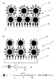
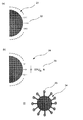
ここで、図1(a)は本発明の第1の実施の形態に係る反射防止膜の断面構造を模式的に表した説明図、図1(b)は本発明の第2の実施の形態に係る反射防止膜の断面構造を模式的に表した説明図、図2は本発明の第1、第2の実施の形態に係る反射防止膜の製造方法において、エポキシ化光学ガラス基材を製造する工程を説明するために分子レベルまで拡大した概念図であり、図2(a)は反応前の光学ガラス基材の断面構造、図2(b)はエポキシ基を有する膜化合物の単分子膜が形成された光学ガラス基材の断面構造をそれぞれ表し、図3は同反射防止膜の製造方法において、エポキシ化シリカ微粒子を製造する工程を説明するために分子レベルまで拡大した概念図であり、図3(a)は反応前のシリカ微粒子の断面構造、図3(b)はエポキシ基を有する膜化合物の単分子膜が形成されたシリカ微粒子の断面構造をそれぞれ表し、図4はエポキシ化光学ガラス基材の表面に、エポキシ基と2−メチルイミダゾールのアミノ基とのカップリング反応により形成された結合を介して固定された2−メチルイミダゾールの被膜を有する反応性光学ガラス基材の断面構造を模式的に表した説明図、図5はエポキシ化シリカ微粒子の表面に、エポキシ基と2−メチルイミダゾールのアミノ基とのカップリング反応により形成された結合を介して固定された2−メチルイミダゾールの被膜を有する反応性シリカ微粒子の断面構造を模式的に表した説明図である。
Next, embodiments of the present invention will be described with reference to the accompanying drawings for understanding of the present invention.
Here, FIG. 1A is an explanatory view schematically showing a cross-sectional structure of the antireflection film according to the first embodiment of the present invention, and FIG. 1B is a second embodiment of the present invention. FIG. 2 is an explanatory view schematically showing a cross-sectional structure of the antireflection film according to the present invention, and FIG. 2 is a method for manufacturing an epoxidized optical glass substrate in the method for manufacturing an antireflection film according to the first and second embodiments of the present invention. FIG. 2 (a) is a cross-sectional structure of an optical glass substrate before reaction, and FIG. 2 (b) is a monomolecular film of a film compound having an epoxy group. Each represents a cross-sectional structure of the optical glass substrate formed, FIG. 3 is a conceptual diagram enlarged to the molecular level to explain the process of producing epoxidized silica fine particles in the production method of the antireflection film, FIG. 3A shows the cross-sectional structure of the silica fine particles before the reaction, and FIG. Represents the cross-sectional structure of silica fine particles on which a monomolecular film of a film compound having an epoxy group is formed. FIG. 4 shows a cup of an epoxy group and an amino group of 2-methylimidazole on the surface of an epoxidized optical glass substrate. FIG. 5 is an explanatory view schematically showing a cross-sectional structure of a reactive optical glass substrate having a 2-methylimidazole film fixed through a bond formed by a ring reaction, and FIG. It is explanatory drawing which represented typically the cross-sectional structure of the reactive silica fine particle which has the film of 2-methylimidazole fixed through the coupling | bonding formed by the coupling reaction of an epoxy group and the amino group of 2-methylimidazole. is there.
次に、本発明の第1の実施の形態に係る反射防止膜1について説明する。
図1(a)に示すように、反射防止膜1は、反応性光学ガラス基材(反応性基材の一例)32の表面に、エポキシ化シリカ微粒子(第1の被覆透明微粒子の一例)24が配列した透明微粒子層が1層結合固定されている。透明微粒子層は、エポキシ化光学ガラス基材14側から空気との界面側に向かって第1層から第n層(nは2以上の整数で、本実施の形態においてはn=2)まで順次積層している。
Next, the antireflection film 1 according to the first embodiment of the present invention will be described.
As shown in FIG. 1A, the antireflection film 1 is formed on the surface of a reactive optical glass substrate (an example of a reactive substrate) 32, and epoxidized silica particles (an example of first coated transparent particles) 24. The transparent fine particle layer in which is arranged is bonded and fixed in one layer. The transparent fine particle layer is sequentially from the first layer to the nth layer (n is an integer of 2 or more, and n = 2 in the present embodiment) from the epoxidized
反応性光学ガラス基材32の表面は、エポキシ基を有する膜化合物(第1の膜化合物の一例)の単分子膜13で被覆され、さらにその表面は、2−メチルイミダゾール(第1のカップリング剤の一例)のアミノ基(第1のカップリング反応基の一例)とエポキシ基とのカップリング反応により形成された結合を介して固定された2−メチルイミダゾールの被膜で被覆されている。
2層目の透明微粒子層を形成しているエポキシ化シリカ微粒子24の表面は、2−メチルイミダゾール(第3のカップリング剤の一例)のアミノ基(第3のカップリング反応基の一例)とエポキシ基とのカップリング反応により形成された結合を介して固定された2−メチルイミダゾールの被膜でさらに被覆されている。
反応性光学ガラス基材32と第1層目の透明微粒子層を形成するエポキシ化シリカ微粒子24、および奇数層目の透明微粒子層を形成するエポキシ化シリカ微粒子24と第2層目の透明微粒子層を形成する反応性シリカ微粒子42との間は、エポキシ基と2−メチルイミダゾールのアミノ基またはイミノ基とのカップリング反応により形成された結合を介して互いに結合固定されている。
The surface of the reactive
The surface of the epoxidized silica
The reactive
反射防止膜1の製造方法は、図2(a)、(b)、図3(a)、(b)、図4、および図5に示すように、エポキシ基を有するアルコキシシラン化合物(第1の膜化合物の一例)を含む溶液を光学ガラス基材(基材の一例)11の表面に接触させ、アルコキシシリル基(第1の結合基の一例)と光学ガラス基材11の表面との間で結合を形成させ、エポキシ化光学ガラス基材14(被覆基材の一例)を調製する工程A(図2参照)と、エポキシ基を有するアルコキシシラン化合物(第2の膜化合物の一例)をシリカ微粒子(透明微粒子の一例)21の表面に接触させ、アルコキシシリル基(第2の結合基の一例)とシリカ微粒子21の表面との間で結合を形成させ、エポキシ化シリカ微粒子24を調製する工程B(図3参照)と、まず、エポキシ化光学ガラス基材14の表面に、2−メチルイミダゾールを接触させ、エポキシ基とアミノ基とをカップリング反応させて反応性光学ガラス基材32を調製し、次いで、反応性光学ガラス基材32の表面にエポキシ化シリカ微粒子24を接触させ、エポキシ基とイミノ基(第2のカップリング反応基の一例)とのカップリング反応により結合を形成させ、エポキシ化光学ガラス基材14の表面にエポキシ化シリカ微粒子24を固定し、次いで、固定されなかったエポキシ化シリカ微粒子24を除去する工程C(図4参照)と、エポキシ化アルコキシシラン化合物(第3の膜化合物の一例)を含む溶液をシリカ微粒子21の表面に接触させ、アルコキシシリル基(第3の結合基の一例)とシリカ微粒子21の表面との間で結合を形成させ、エポキシ化シリカ微粒子(第2の被覆透明微粒子の一例)24を調製し、次いで、エポキシ化シリカ微粒子24の表面に、2−メチルイミダゾール(第2のカップリング剤の一例)を接触させ、エポキシ基(第3の官能基の一例)とアミノ基とのカップリング反応により形成させた結合を介して固定された2−メチルイミダゾールの形成する被膜を表面に有する反応性シリカ微粒子(第2の反応性透明微粒子の一例)42を調製する工程D(図5参照)と、エポキシ化シリカ微粒子24の透明微粒子層を有する反射防止膜1の表面に反応性シリカ微粒子42を接触させ、エポキシ基とイミノ基とのカップリング反応により結合を形成させ、反応性シリカ微粒子42をエポキシ化シリカ微粒子24の透明微粒子層の上に結合固定し、次いで、結合固定されなかった反応性シリカ微粒子42を除去する工程Eと、反応性シリカ微粒子42の透明微粒子層を有する反射防止膜1の表面にエポキシ化シリカ微粒子24を接触させ、エポキシ基とイミノ基とのカップリング反応により結合を形成させ、エポキシ化シリカ微粒子24を反応性シリカ微粒子42の透明微粒子層の上に結合固定し、次いで、結合固定されなかったエポキシ化シリカ微粒子24を除去する工程Fとを有する。
As shown in FIGS. 2 (a), 2 (b), 3 (a), 3 (b), 4 and 5, the production method of the antireflection film 1 is an alkoxysilane compound having an epoxy group (first A solution containing an example of the film compound of the above is brought into contact with the surface of the optical glass substrate (an example of the substrate) 11, and between the alkoxysilyl group (an example of the first bonding group) and the surface of the
以下、工程A〜Fについてより詳細に説明する。
工程Aでは、エポキシ基を有する膜化合物を光学ガラス基材11に接触させ、エポキシ基を有する膜化合物の単分子膜13で表面が覆われたエポキシ化光学ガラス基材14を製造する(図2)。
なお、光学ガラス基材11の形状および大きさには特に制限はない。光学ガラス基材の具体例としては、カメラ、眼鏡、望遠鏡、顕微鏡、液晶プロジェクタ等のレンズ、CRT、LCD、および有機EL等の各種表示装置用ガラス板、反射望遠鏡等の反射鏡、コピー機、フラットヘッドスキャナ等の原稿台ガラス等が挙げられる。
Hereinafter, the steps A to F will be described in more detail.
In step A, a film compound having an epoxy group is brought into contact with the
The shape and size of the
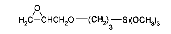
エポキシ基を有する膜化合物としては、光学ガラス基材11の表面に吸着または結合し、自己組織化により単分子膜を形成することのできる任意の化合物を用いることができるが、直鎖状アルキレン基の一方の末端にエポキシ基(オキシラン環)を含む官能基を、他方の末端にアルコキシシリル基(第1の結合基の一例)をそれぞれ有し、下記の一般式(化1)で表されるアルコキシシラン化合物が好ましい。
As the film compound having an epoxy group, any compound that can be adsorbed or bonded to the surface of the
![]()
![]()
上式において、官能基Eはエポキシ基を有する官能基を、mは3〜20の整数を、Rは炭素数1〜4のアルキル基をそれぞれ表す。
用いることのできるエポキシ基を有する膜化合物の具体例としては、下記(1)〜(12)に示したアルコキシシラン化合物が挙げられる。
In the above formula, functional group E represents a functional group having an epoxy group, m represents an integer of 3 to 20, and R represents an alkyl group having 1 to 4 carbon atoms.
Specific examples of the film compound having an epoxy group that can be used include alkoxysilane compounds shown in the following (1) to (12).
(1) (CH2OCH)CH2O(CH2)3Si(OCH3)3
(2) (CH2OCH)CH2O(CH2)7Si(OCH3)3
(3) (CH2OCH)CH2O(CH2)11Si(OCH3)3
(4) (CH2CHOCH(CH2)2)CH(CH2)2Si(OCH3)3
(5) (CH2CHOCH(CH2)2)CH(CH2)4Si(OCH3)3
(6) (CH2CHOCH(CH2)2)CH(CH2)6Si(OCH3)3
(7) (CH2OCH)CH2O(CH2)3Si(OC2H5)3
(8) (CH2OCH)CH2O(CH2)7Si(OC2H5)3
(9) (CH2OCH)CH2O(CH2)11Si(OC2H5)3
(10) (CH2CHOCH(CH2)2)CH(CH2)2Si(OC2H5)3
(11) (CH2CHOCH(CH2)2)CH(CH2)4Si(OC2H5)3
(12) (CH2CHOCH(CH2)2)CH(CH2)6Si(OC2H5)3
(1) (CH 2 OCH) CH 2 O (CH 2 ) 3 Si (OCH 3 ) 3
(2) (CH 2 OCH) CH 2 O (CH 2) 7 Si (OCH 3) 3
(3) (CH 2 OCH) CH 2 O (CH 2) 11 Si (OCH 3) 3
(4) (CH 2 CHOCH ( CH 2) 2) CH (CH 2) 2 Si (OCH 3) 3
(5) (CH 2 CHOCH ( CH 2) 2) CH (CH 2) 4 Si (OCH 3) 3
(6) (CH 2 CHOCH ( CH 2) 2) CH (CH 2) 6 Si (OCH 3) 3
(7) (CH 2 OCH) CH 2 O (CH 2) 3 Si (OC 2 H 5) 3
(8) (CH 2 OCH) CH 2 O (CH 2) 7 Si (OC 2 H 5) 3
(9) (CH 2 OCH) CH 2 O (CH 2 ) 11 Si (OC 2 H 5 ) 3
(10) (CH 2 CHOCH ( CH 2) 2) CH (CH 2) 2 Si (OC 2 H 5) 3
(11) (CH 2 CHOCH ( CH 2) 2) CH (CH 2) 4 Si (OC 2 H 5) 3
(12) (CH 2 CHOCH ( CH 2) 2) CH (CH 2) 6 Si (OC 2 H 5) 3
ここで、(CH2OCH)CH2O−基は、化2で表される官能基(グリシジルオキシ基)を表し、(CH2CHOCH(CH2)2)CH−基は、化3で表される官能基(3,4−エポキシシクロヘキシル基)を表す。 Here, the (CH 2 OCH) CH 2 O— group represents a functional group (glycidyloxy group) represented by Chemical Formula 2 , and the (CH 2 CHOCH (CH 2 ) 2 ) CH— group is represented by Chemical Formula 3. Represents a functional group (3,4-epoxycyclohexyl group).
エポキシ化光学ガラス基材14の製造は、エポキシ基およびアルコキシシリル基(第2の結合基の一例)を含むアルコキシシラン化合物と、アルコキシシリル基と光学ガラス基材11の表面のヒドロキシル基12との縮合反応を促進するための縮合触媒と、非水系の有機溶媒とを混合した反応液を光学ガラス基材11の表面に塗布し、室温の空気中で反応させることにより行われる。塗布は、ドクターブレード法、ディップコート法、スピンコート法、スプレー法、スクリーン印刷法等の任意の方法により行うことができる。
The production of the epoxidized
縮合触媒としては、カルボン酸金属塩、カルボン酸エステル金属塩、カルボン酸金属塩ポリマー、カルボン酸金属塩キレート、チタン酸エステルおよびチタン酸エステルキレート等の金属塩が利用可能である。
縮合触媒の添加量は、好ましくはアルコキシシラン化合物の0.2〜5質量%であり、より好ましくは0.5〜1質量%である。
As the condensation catalyst, metal salts such as carboxylic acid metal salts, carboxylic acid ester metal salts, carboxylic acid metal salt polymers, carboxylic acid metal salt chelates, titanate esters and titanate ester chelates can be used.
The addition amount of the condensation catalyst is preferably 0.2 to 5% by mass of the alkoxysilane compound, and more preferably 0.5 to 1% by mass.
カルボン酸金属塩の具体例としては、酢酸第1スズ、ジブチルスズジラウレート、ジブチルスズジオクテート、ジブチルスズジアセテート、ジオクチルスズジラウレート、ジオクチルスズジオクテート、ジオクチルスズジアセテート、ジオクタン酸第1スズ、ナフテン酸鉛、ナフテン酸コバルト、2−エチルヘキセン酸鉄が挙げられる。 Specific examples of carboxylic acid metal salts include stannous acetate, dibutyltin dilaurate, dibutyltin dioctate, dibutyltin diacetate, dioctyltin dilaurate, dioctyltin dioctate, dioctyltin diacetate, stannous dioctanoate, naphthenic acid Lead, cobalt naphthenate, and iron 2-ethylhexenoate.
カルボン酸エステル金属塩の具体例としては、ジオクチルスズビスオクチリチオグリコール酸エステル塩、ジオクチルスズマレイン酸エステル塩が挙げられる。
カルボン酸金属塩ポリマーの具体例としては、ジブチルスズマレイン酸塩ポリマー、ジメチルスズメルカプトプロピオン酸塩ポリマーが挙げられる。
カルボン酸金属塩キレートの具体例としては、ジブチルスズビスアセチルアセテート、ジオクチルスズビスアセチルラウレートが挙げられる。
Specific examples of the carboxylic acid ester metal salt include dioctyltin bisoctylthioglycolate ester salt and dioctyltin maleate ester salt.
Specific examples of the carboxylic acid metal salt polymer include dibutyltin maleate polymer and dimethyltin mercaptopropionate polymer.
Specific examples of the carboxylic acid metal salt chelate include dibutyltin bisacetylacetate and dioctyltin bisacetyllaurate.
チタン酸エステルの具体例としては、テトラブチルチタネート、テトラノニルチタネートが挙げられる。
チタン酸エステルキレート類の具体例としては、ビス(アセチルアセトニル)ジ−プロピルチタネートが挙げられる。
Specific examples of the titanate ester include tetrabutyl titanate and tetranonyl titanate.
Specific examples of titanate chelates include bis (acetylacetonyl) dipropyl titanate.
アルコキシシリル基と光学ガラス基材11の表面のヒドロキシル基12とが縮合反応を起こし、下記の化4で示されるような構造を有するエポキシ基を有する膜化合物の単分子膜13を生成する。なお、酸素原子から延びた3本の単結合は光学ガラス基材11の表面または隣接するシラン化合物のケイ素(Si)原子と結合しており、そのうち少なくとも1本は光学ガラス基材11の表面のケイ素原子と結合している。
The alkoxysilyl group and the
アルコキシシリル基は、水分の存在下で分解するので、反応は相対湿度45%以下の空気中で行うことが好ましい。なお、縮合反応は、光学ガラス基材11の表面に付着した油脂分や水分により阻害されるので、光学ガラス基材11をよく洗浄して乾燥することにより、これらの不純物を予め除去しておくことが好ましい。
縮合触媒として上述の金属塩のいずれかを用いた場合、縮合反応の完了までに要する時間は2時間程度である。
Since the alkoxysilyl group decomposes in the presence of moisture, the reaction is preferably performed in air with a relative humidity of 45% or less. The condensation reaction is hindered by oils and fats and moisture adhering to the surface of the
When any of the above metal salts is used as the condensation catalyst, the time required for completion of the condensation reaction is about 2 hours.
上述の金属塩の代わりに、ケチミン化合物、有機酸、アルジミン化合物、エナミン化合物、オキサゾリジン化合物、アミノアルキルアルコキシシラン化合物からなる群より選択される1または2以上の化合物を縮合触媒として用いた場合、反応時間を1/2〜2/3程度まで短縮できる。 When one or more compounds selected from the group consisting of ketimine compounds, organic acids, aldimine compounds, enamine compounds, oxazolidine compounds, and aminoalkylalkoxysilane compounds are used as the condensation catalyst instead of the above metal salts, Time can be shortened to about 1/2 to 2/3.
あるいは、これらの化合物を助触媒として、上述の金属塩と混合(質量比1:9〜9:1の範囲で使用可能だが、1:1前後が好ましい)して用いると、反応時間をさらに短縮できる。 Alternatively, when these compounds are used as a co-catalyst and mixed with the above-described metal salt (mass ratio 1: 9 to 9: 1 can be used, preferably around 1: 1), the reaction time is further shortened. it can.
例えば、縮合触媒として、ジブチルスズオキサイドの代わりにケチミン化合物であるジャパンエポキシレジン社のH3を用い、その他の条件は同一にしてエポキシ化シリカ微粒子24の製造を行うと、エポキシ化シリカ微粒子24の品質を損なうことなく反応時間を1時間程度にまで短縮できる。
For example, when H3 from Japan Epoxy Resin Co., Ltd., which is a ketimine compound, is used instead of dibutyltin oxide as the condensation catalyst, and the other conditions are the same, the quality of the epoxidized silica
さらに、縮合触媒として、ジャパンエポキシレジン社のH3とジブチルスズビスアセチルアセトネートとの混合物(混合比は1:1)を用い、その他の条件は同一にしてエポキシ化シリカ微粒子24の製造を行うと、反応時間を20分程度に短縮できる。
Furthermore, when a mixture of H3 and dibutyltin bisacetylacetonate of Japan Epoxy Resin Co., Ltd. (mixing ratio is 1: 1) is used as the condensation catalyst, and the other conditions are the same, the epoxidized silica
なお、ここで用いることができるケチミン化合物は特に限定されるものではないが、例えば、2,5,8−トリアザ−1,8−ノナジエン、3,11−ジメチル−4,7,10−トリアザ−3,10−トリデカジエン、2,10−ジメチル−3,6,9−トリアザ−2,9−ウンデカジエン、2,4,12,14−テトラメチル−5,8,11−トリアザ−4,11−ペンタデカジエン、2,4,15,17−テトラメチル−5,8,11,14−テトラアザ−4,14−オクタデカジエン、2,4,20,22−テトラメチル−5,12,19−トリアザ−4,19−トリエイコサジエン等が挙げられる。 The ketimine compound that can be used here is not particularly limited, and examples thereof include 2,5,8-triaza-1,8-nonadiene, 3,11-dimethyl-4,7,10-triaza- 3,10-tridecadiene, 2,10-dimethyl-3,6,9-triaza-2,9-undecadiene, 2,4,12,14-tetramethyl-5,8,11-triaza-4,11-penta Decadiene, 2,4,15,17-tetramethyl-5,8,11,14-tetraaza-4,14-octadecadiene, 2,4,20,22-tetramethyl-5,12,19-triaza -4,19-trieicosadiene and the like.
また、用いることができる有機酸としても特に限定されるものではないが、例えば、ギ酸、酢酸、プロピオン酸、酪酸、マロン酸等が挙げられる。 Moreover, although it does not specifically limit as an organic acid which can be used, For example, a formic acid, an acetic acid, propionic acid, a butyric acid, malonic acid etc. are mentioned.
反応液の製造には、有機塩素系溶媒、炭化水素系溶媒、フッ化炭素系溶媒、シリコーン系溶媒、およびこれらの混合溶媒を用いることができる。アルコキシシラン化合物の加水分解を防止するために、乾燥剤または蒸留により使用する溶媒から水分を除去しておくことが好ましい。また、溶媒の沸点は50〜250℃であることが好ましい。 For the production of the reaction solution, an organic chlorine solvent, a hydrocarbon solvent, a fluorocarbon solvent, a silicone solvent, and a mixed solvent thereof can be used. In order to prevent hydrolysis of the alkoxysilane compound, it is preferable to remove water from the desiccant or the solvent used by distillation. Moreover, it is preferable that the boiling point of a solvent is 50-250 degreeC.
具体的に使用可能な溶媒としては、非水系の石油ナフサ、ソルベントナフサ、石油エーテル、石油ベンジン、イソパラフィン、ノルマルパラフィン、デカリン、工業ガソリン、ノナン、デカン、灯油、ジメチルシリコーン、フェニルシリコーン、アルキル変性シリコーン、ポリエーテルシリコーン、ジメチルホルムアミド等を挙げることができる。
さらに、メタノール、エタノール、プロパノール等のアルコール系溶媒、あるいはそれらの混合物を用いることもできる。
Specific usable solvents include non-aqueous petroleum naphtha, solvent naphtha, petroleum ether, petroleum benzine, isoparaffin, normal paraffin, decalin, industrial gasoline, nonane, decane, kerosene, dimethyl silicone, phenyl silicone, and alkyl-modified silicone. , Polyether silicone, dimethylformamide and the like.
Furthermore, alcohol solvents such as methanol, ethanol, propanol, or a mixture thereof can also be used.
また、用いることができるフッ化炭素系溶媒としては、フロン系溶媒、フロリナート(米国3M社製)、アフルード(旭硝子株式会社製)等がある。なお、これらは1種単独で用いても良いし、良く混ざるものなら2種以上を組み合わせてもよい。さらに、ジクロロメタン、クロロホルム等の有機塩素系溶媒を添加してもよい。 Fluorocarbon solvents that can be used include fluorocarbon solvents, Fluorinert (manufactured by 3M, USA), Afludo (manufactured by Asahi Glass Co., Ltd.), and the like. In addition, these may be used individually by 1 type and may mix 2 or more types as long as it mixes well. Furthermore, an organic chlorine solvent such as dichloromethane or chloroform may be added.
反応液におけるアルコキシシラン化合物の好ましい濃度は、0.5〜3質量%である。 The preferable density | concentration of the alkoxysilane compound in a reaction liquid is 0.5-3 mass%.
反応後、溶媒で洗浄し、未反応物として表面に残った余分なアルコキシシラン化合物および縮合触媒を除去すると、エポキシ基を有する膜化合物の単分子膜13で表面が覆われたエポキシ化光学ガラス基材14が得られる。このようにして製造されるエポキシ化光学ガラス基材14の断面構造の模式図を図2(b)に示す。
After the reaction, the epoxidized optical glass group whose surface is covered with a
洗浄溶媒としては、アルコキシシラン化合物を溶解できる任意の溶媒を用いることができるが、安価であり、溶解性が高く、風乾により容易に除去することのできるジクロロメタン、クロロホルム、N−メチルピロリドン等が好ましい。 As the cleaning solvent, any solvent that can dissolve the alkoxysilane compound can be used, but dichloromethane, chloroform, N-methylpyrrolidone, etc. that are inexpensive, have high solubility, and can be easily removed by air drying are preferable. .
反応後、生成したエポキシ化光学ガラス基材14を溶媒で洗浄せずに空気中に放置すると、表面に残ったアルコキシシラン化合物の一部が空気中の水分により加水分解を受け、生成したシラノール基がアルコキシシリル基と縮合反応を起こす。その結果、エポキシ化光学ガラス基材14の表面にポリシロキサンよりなる極薄のポリマー膜が形成される。このポリマー膜は、エポキシ化光学ガラス基材14の表面に必ずしも共有結合により固定されていないが、エポキシ基を含んでいるため、エポキシ化光学ガラス基材14に対してエポキシ基を有する膜化合物の単分子膜13と同様の反応性を有している。そのため、洗浄を行わなくても、工程C以降の製造工程に特に支障をきたすことはない。
After the reaction, when the produced epoxidized
なお、本実施の形態においては、エポキシ基を有するアルコキシシラン化合物を用いたが、直鎖状アルキレン基の一方の末端にアミノ基を、他方の末端にアルコキシシリル基をそれぞれ有し、下記の一般式(化5)で表されるアルコキシシラン化合物を用いてもよい。なお、アミノ基と反応するカップリング剤としては、両端にグリシジル基を有する化合物が使用できる。 In the present embodiment, an alkoxysilane compound having an epoxy group is used. However, the linear alkylene group has an amino group at one end and an alkoxysilyl group at the other end. An alkoxysilane compound represented by the formula (Formula 5) may be used. In addition, as a coupling agent which reacts with an amino group, the compound which has a glycidyl group at both ends can be used.
![]()
![]()
上式において、mは3〜20の整数を、Rは炭素数1〜4のアルキル基をそれぞれ表す。
用いることのできるアミノ基を有する膜化合物の具体例としては、下記(21)〜(28)に示したアルコキシシラン化合物が挙げられる。
In the above formula, m represents an integer of 3 to 20, and R represents an alkyl group having 1 to 4 carbon atoms.
Specific examples of the film compound having an amino group that can be used include alkoxysilane compounds shown in the following (21) to (28).
(21) H2N(CH2)3Si(OCH3)3
(22) H2N(CH2)5Si(OCH3)3
(23) H2N(CH2)7Si(OCH3)3
(24) H2N(CH2)9Si(OCH3)3
(25) H2N(CH2)5Si(OC2H5)3
(26) H2N(CH2)5Si(OC2H5)3
(27) H2N(CH2)7Si(OC2H5)3
(28) H2N(CH2)9Si(OC2H5)3
(21) H 2 N (CH 2 ) 3 Si (OCH 3 ) 3
(22) H 2 N (CH 2 ) 5 Si (OCH 3 ) 3
(23) H 2 N (CH 2 ) 7 Si (OCH 3 ) 3
(24) H 2 N (CH 2 ) 9 Si (OCH 3 ) 3
(25) H 2 N (CH 2) 5 Si (OC 2 H 5) 3
(26) H 2 N (CH 2 ) 5 Si (OC 2 H 5 ) 3
(27) H 2 N (CH 2 ) 7 Si (OC 2 H 5 ) 3
(28) H 2 N (CH 2 ) 9 Si (OC 2 H 5 ) 3
ただし、この場合に反応液において用いることのできる縮合触媒のうち、スズ(Sn)塩を含む化合物は、アミノ基と反応して沈殿を生成するため、アミノ基を有するアルコキシシラン化合物に対しては縮合触媒として用いることができない。
したがって、アミノ基を有するアルコキシシラン化合物を用いる場合には、カルボン酸スズ塩、カルボン酸エステルスズ塩、カルボン酸スズ塩ポリマー、カルボン酸スズ塩キレートを除き、エポキシ基を有するアルコキシシラン化合物の場合と同様の化合物を単独でまたは2種類以上を混合して縮合触媒として用いることができる。
用いることのできる助触媒の種類およびそれらの組み合わせ、溶媒の種類、アルコキシシラン化合物、縮合触媒、および助触媒の濃度、反応条件ならびに反応時間についてはエポキシ基を有するアルコキシシラン化合物の場合と同様であるので、説明を省略する。
However, among the condensation catalysts that can be used in the reaction solution in this case, a compound containing a tin (Sn) salt reacts with an amino group to form a precipitate, so that for an alkoxysilane compound having an amino group, It cannot be used as a condensation catalyst.
Therefore, when using an alkoxysilane compound having an amino group, excluding carboxylic acid tin salt, carboxylic acid ester tin salt, carboxylic acid tin salt polymer, carboxylic acid tin salt chelate, and an alkoxysilane compound having an epoxy group Similar compounds can be used alone or in combination of two or more as a condensation catalyst.
The types of cocatalysts that can be used and combinations thereof, the types of solvents, the concentration of alkoxysilane compounds, condensation catalysts, and cocatalysts, reaction conditions, and reaction times are the same as in the case of alkoxysilane compounds having an epoxy group. Therefore, explanation is omitted.
本実施の形態においては、各種光学機器に用いられる光学ガラス基材を基材として用いたが、自動車、鉄道車両、および船舶等のフロントスクリーン用ガラス等を基材として用いてもよい。
また、その表面にヒドロキシル基、アミノ基等の活性水素基を有する透明な合成樹脂等も基材として用いることができる。
(以上工程A)
In the present embodiment, an optical glass base material used for various optical devices is used as a base material, but glass for front screens of automobiles, railway vehicles, ships, etc. may be used as the base material.
A transparent synthetic resin having an active hydrogen group such as a hydroxyl group or an amino group on its surface can also be used as a substrate.
(End of process A)
工程Bでは、工程Aにおいて用いたものと同様のエポキシ基を有する膜化合物をシリカ微粒子21と接触させ、エポキシ基を有する膜化合物の単分子膜23で表面が覆われたエポキシ化シリカ微粒子24を製造する(図3)。
In step B, a film compound having an epoxy group similar to that used in step A is brought into contact with silica
用いることのできるシリカ微粒子21の粒径は、製造される反射防止膜の膜厚、屈折率、および空隙率等に応じて適宜決定されるが、可視光の散乱を防止するために可視光波長(380〜700nm)より小さくなければならない。
具体的には、微粒子の直径は10〜400nmであることが好ましく、10〜300nmであることがより好ましく、10〜100nmであることがさらに好ましい。
The particle diameter of the silica
Specifically, the diameter of the fine particles is preferably 10 to 400 nm, more preferably 10 to 300 nm, and even more preferably 10 to 100 nm.
エポキシ化シリカ微粒子24の製造は、エポキシ基を含むアルコキシシラン化合物と、アルコキシシリル基とシリカ微粒子21の表面のヒドロキシル基22との縮合反応を促進するための縮合触媒と、非水系の有機溶媒とを混合した反応液中にシリカ微粒子21を分散させ、室温の空気中で反応させることにより行われる。
The production of the epoxidized silica
工程Bにおいて用いることのできるエポキシ基を有するアルコキシシラン化合物の種類、縮合触媒、助触媒の種類およびそれらの組み合わせ、溶媒の種類、アルコキシシラン化合物、縮合触媒、および助触媒の濃度、反応条件ならびに反応時間については工程Aと同様であるので、説明を省略する。 Types of alkoxysilane compounds having an epoxy group that can be used in Step B, types of condensation catalysts, types of promoters and combinations thereof, types of solvents, concentrations of alkoxysilane compounds, condensation catalysts, and promoters, reaction conditions and reactions Since the time is the same as in step A, the description is omitted.
反応後、溶媒で洗浄し、未反応物として表面に残った余分なアルコキシシラン化合物および縮合触媒を除去すると、エポキシ基を有する膜化合物の単分子膜23で表面が覆われたエポキシ化シリカ微粒子24が得られる。このようにして製造されるエポキシ化シリカ微粒子24の断面構造の模式図を図3(b)に示す。
After the reaction, washing with a solvent to remove excess alkoxysilane compound and condensation catalyst remaining on the surface as unreacted substances, the epoxidized silica
洗浄溶媒としては、工程Aと同様の洗浄溶媒を用いることができる。
反応後、生成したエポキシ化シリカ微粒子24を溶媒で洗浄せずに空気中に放置すると、表面に残ったアルコキシシラン化合物の一部が空気中の水分により加水分解を受け、生成したシラノール基がアルコキシシリル基と縮合反応を起こす。その結果、エポキシ化シリカ微粒子24の表面にポリシロキサンよりなる極薄のポリマー膜が形成される。このポリマー膜は、エポキシ化シリカ微粒子24の表面に全てが共有結合により固定されているわけではないが、エポキシ基を含んでいるため、エポキシ化シリカ微粒子24に対してエポキシ基を有する膜化合物の単分子膜23と同様の反応性を有している。そのため、洗浄を行わなくても、工程C以降の製造工程に特に支障をきたすことはない。
As the washing solvent, the same washing solvent as in step A can be used.
After the reaction, if the produced epoxidized silica
なお、本実施の形態においてはエポキシ基を有するアルコキシシラン化合物を用いたが、工程Aと同様、直鎖状アルキレン基の一方の末端にアミノ基を、他方の末端にアルコキシシリル基をそれぞれ有するアルコキシシラン化合物を用いてもよい。
また、本実施の形態においては工程Aと同一のアルコキシシラン化合物を用いているが、異なるアルコキシシラン化合物を用いてもよい。ただし、工程Cにおいて用いるカップリング剤のカップリング反応基と反応して結合を形成する官能基を有するものでなければならない。
In this embodiment, an alkoxysilane compound having an epoxy group is used. However, as in Step A, an alkoxy group having an amino group at one end of a linear alkylene group and an alkoxysilyl group at the other end is used. Silane compounds may be used.
In the present embodiment, the same alkoxysilane compound as in step A is used, but a different alkoxysilane compound may be used. However, it must have a functional group that reacts with the coupling reactive group of the coupling agent used in Step C to form a bond.
また、本実施の形態においては、透明微粒子としてシリカ微粒子を用いたが、透明であり、かつ膜化合物と結合の形成が可能な官能基を表面に有する任意の微粒子を用いることができる。用いることができる透明微粒子としては、アルミナ、ジルコニア等の無機微粒子、有機微粒子、有機−無機ハイブリッド微粒子等が挙げられる。 In the present embodiment, silica fine particles are used as the transparent fine particles. However, any fine particles that are transparent and have functional groups that can form bonds with the film compound on the surface can be used. Examples of the transparent fine particles that can be used include inorganic fine particles such as alumina and zirconia, organic fine particles, and organic-inorganic hybrid fine particles.
シリカ微粒子以外の微粒子であっても、その表面に水酸基、アミノ基等の活性水素基を有する場合には、膜化合物としてアルコキシシラン化合物を用いることができる。この様な透明微粒子の具体例としては、アルミナ、ジルコニア等が挙げられる。 Even in the case of fine particles other than silica fine particles, an alkoxysilane compound can be used as the film compound when the surface has active hydrogen groups such as hydroxyl groups and amino groups. Specific examples of such transparent fine particles include alumina and zirconia.
本実施の形態においては、第1および第2の膜化合物として、ともにエポキシ基を有する膜化合物を用いているが、両者は同一の化合物であってもよく、また異なる化合物であってもよい。さらに、第1および第2の膜化合物が異なる官能基(例えば、一方がエポキシ基で他方がイソシアネート基)を有していてもよい。
(以上工程B)
In the present embodiment, as the first and second film compounds, film compounds having an epoxy group are used, but both may be the same compound or different compounds. Furthermore, the first and second film compounds may have different functional groups (for example, one is an epoxy group and the other is an isocyanate group).
(End of process B)
工程Cでは、まず、エポキシ化光学ガラス基材14の表面に、2−メチルイミダゾールを接触させ、エポキシ基とアミノ基とをカップリング反応させて反応性光学ガラス基材32を調製し、次いで、反応性光学ガラス基材32の表面にエポキシ化シリカ微粒子24を接触させ、エポキシ基とイミノ基とのカップリング反応により結合を形成させ、エポキシ化光学ガラス基材14の表面にエポキシ化シリカ微粒子24を固定し、次いで、固定されなかったエポキシ化シリカ微粒子24を除去する
In Step C, first, 2-methylimidazole is brought into contact with the surface of the epoxidized
2−メチルイミダゾールはエポキシ基と反応するアミノ基およびイミノ基をそれぞれ1−位および3−位に有しており、下記の化6に示すような架橋反応により結合を形成する。 2-Methylimidazole has an amino group and an imino group that react with an epoxy group at the 1-position and 3-position, respectively, and forms a bond by a crosslinking reaction as shown in Chemical Formula 6 below.
反応性光学ガラス基材32の製造は、2−メチルイミダゾールと溶媒とを混合した反応液をエポキシ化光学ガラス基材14の表面に塗布し、加熱して反応させることにより行われる。塗布は、ドクターブレード法、ディップコート法、スピンコート法、スプレー法、スクリーン印刷法等の任意の方法により行うことができる。
膜前駆体の製造には、2−メチルイミダゾールが可溶な任意の溶媒を用いることができるが、価格、室温での揮発性、および毒性等を考慮すると、イソプロピルアルコール、エタノール等の低級アルコール系溶媒が好ましい。
2−メチルイミダゾールの添加量、塗布する溶液の濃度、反応温度および反応時間は、用いる基材および微粒子の種類、形成する反射防止膜の膜厚等に応じて適宜調節される。
The production of the reactive
For the production of the film precursor, any solvent in which 2-methylimidazole is soluble can be used. However, considering the price, volatility at room temperature, toxicity, etc., lower alcohols such as isopropyl alcohol and ethanol are used. A solvent is preferred.
The addition amount of 2-methylimidazole, the concentration of the solution to be applied, the reaction temperature and the reaction time are appropriately adjusted according to the type of substrate and fine particles used, the thickness of the antireflection film to be formed, and the like.
反応後、溶媒で洗浄し、未反応物として表面に残った余分な2−メチルイミダゾールを除去すると、反応性単分子膜31で表面が覆われた反応性光学ガラス基材32が得られる(図4)。
After the reaction, the substrate is washed with a solvent to remove excess 2-methylimidazole remaining on the surface as an unreacted material, thereby obtaining a reactive
このようにして得られた反応性光学ガラス基材32の表面にエポキシ化シリカ微粒子24の分散液を塗布後加熱し、エポキシ化シリカ微粒子24上のエポキシ基と、反応性単分子膜31上の2−メチルイミダゾールに由来するイミノ基とのカップリング反応によりエポキシ化シリカ微粒子24を反応性光学ガラス基材32の表面に結合固定し、単層の透明微粒子層を有する反射防止膜1を製造する。
加熱温度は、100〜200℃が好ましい。加熱温度が100℃未満だと、カップリング反応の進行に長時間を要し、200℃を上回ると、エポキシ基を有する単分子膜23や反応性単分子膜31の分解反応が起こり、均一な反射防止膜1が得られない。
The dispersion of the epoxidized silica
The heating temperature is preferably 100 to 200 ° C. When the heating temperature is less than 100 ° C., it takes a long time for the coupling reaction to proceed, and when it exceeds 200 ° C., the decomposition reaction of the
反応後、水やアルコール等の溶媒で洗浄することにより、過剰のエポキシ化シリカ微粒子24を除去する。
After the reaction, excess epoxidized silica
本実施の形態においては、カップリング剤として2−メチルイミダゾールを用いたが、下記化7で表される任意のイミダゾール誘導体を用いることができる。 In the present embodiment, 2-methylimidazole is used as a coupling agent, but any imidazole derivative represented by the following chemical formula 7 can be used.
化7で表されるイミダゾール誘導体の具体例としては、下記(31)〜(38)に示すものが挙げられる。
(31) 2−メチルイミダゾール(R2=Me、R4=R5=H)
(32) 2−ウンデシルイミダゾール(R2=C11H23、R4=R5=H)
(33) 2−ペンタデシルイミダゾール(R2=C15H31、R4=R5=H)
(34) 2−メチル−4−エチルイミダゾール(R2=Me、R4=Et、R5=H)
(35) 2−フェニルイミダゾール(R2=Ph、R4=R5=H)
(36) 2−フェニル−4−エチルイミダゾール(R2=Ph、R4=Et、R5=H)
(37) 2−フェニル−4−メチル−5−ヒドロキシメチルイミダゾール(R2=Ph、R4=Me、R5=CH2OH)
(38) 2−フェニル−4,5−ビス(ヒドロキシメチル)イミダゾール(R2=Ph、R4=R5=CH2OH)
なお、Me、Et、およびPhは、それぞれメチル基、エチル基、およびフェニル基を表す。
Specific examples of the imidazole derivative represented by Chemical Formula 7 include those shown in the following (31) to (38).
(31) 2-Methylimidazole (R 2 = Me, R 4 = R 5 = H)
(32) 2-Undecylimidazole (R 2 = C 11 H 23 , R 4 = R 5 = H)
(33) 2-Pentadecylimidazole (R 2 = C 15 H 31 , R 4 = R 5 = H)
(34) 2-methyl-4-ethylimidazole (R 2 = Me, R 4 = Et, R 5 = H)
(35) 2-Phenylimidazole (R 2 = Ph, R 4 = R 5 = H)
(36) 2-phenyl-4-ethylimidazole (R 2 = Ph, R 4 = Et, R 5 = H)
(37) 2-phenyl-4-methyl-5-hydroxymethylimidazole (R 2 = Ph, R 4 = Me, R 5 =
(38) 2-Phenyl-4,5-bis (hydroxymethyl) imidazole (R 2 = Ph, R 4 = R 5 = CH 2 OH)
Me, Et, and Ph represent a methyl group, an ethyl group, and a phenyl group, respectively.
また、エポキシ樹脂の硬化剤として用いられる無水フタル酸、無水マレイン酸等の酸無水物、ジシアンジアミド、ノボラック等のフェノール誘導体等の化合物をカップリング剤として用いてもよい。この場合、カップリング反応を促進するためにイミダゾール誘導体を触媒として用いてもよい。 In addition, compounds such as acid anhydrides such as phthalic anhydride and maleic anhydride, and phenol derivatives such as dicyandiamide and novolak, which are used as a curing agent for epoxy resins, may be used as a coupling agent. In this case, an imidazole derivative may be used as a catalyst in order to accelerate the coupling reaction.
なお、本実施の形態においては官能基としてエポキシ基を有する膜化合物を用いた場合について説明しているが、官能基としてアミノ基またはイミノ基を有する膜化合物を用いる場合には、カップリング反応基として2もしくは3以上のエポキシ基または2もしくは3以上のイソシアネート基を有するカップリング剤を用いる。イソシアネート基を有する化合物の具体例としては、p−フェニレンジイソシアネート、ヘキサメチレン−1,6−ジイソシアネート、トルエン−2,6−ジイソシアネート、トルエン−2,4−ジイソシアネート等が挙げられる。
これらのジイソシアネート化合物の添加量は、2−メチルイミダゾールの場合と同様、エポキシ化シリカ微粒子の5〜15重量%が好ましい。この場合、膜前駆体の製造に用いることのできる溶媒としては、キシレン等の芳香族有機溶媒が挙げられる。
また、アミノ基を有する膜化合物を用いる場合には、架橋剤としては、エチレングリコールジグリシジルエーテル等の2または3以上のエポキシ基を有する化合物を用いることもできる。
(以上工程C)
In this embodiment, the case of using a film compound having an epoxy group as a functional group is described. However, when a film compound having an amino group or an imino group as a functional group is used, a coupling reactive group is used. A coupling agent having 2 or 3 or more epoxy groups or 2 or 3 or more isocyanate groups is used. Specific examples of the compound having an isocyanate group include p-phenylene diisocyanate, hexamethylene-1,6-diisocyanate, toluene-2,6-diisocyanate, toluene-2,4-diisocyanate and the like.
The addition amount of these diisocyanate compounds is preferably 5 to 15% by weight of the epoxidized silica fine particles as in the case of 2-methylimidazole. In this case, examples of the solvent that can be used for the production of the film precursor include aromatic organic solvents such as xylene.
Moreover, when using the film | membrane compound which has an amino group, the compound which has 2 or 3 or more epoxy groups, such as ethylene glycol diglycidyl ether, can also be used as a crosslinking agent.
(End of process C)
工程Dでは、エポキシ化アルコキシシラン化合物を含む溶液をシリカ微粒子21の表面に接触させ、アルコキシシリル基とシリカ微粒子21の表面との間で結合を形成させ、エポキシ化シリカ微粒子24を調製し、次いで、エポキシ化シリカ微粒子24の表面に、2−メチルイミダゾールを接触させ、エポキシ基と2−メチルイミダゾールに由来するアミノ基とのカップリング反応により形成させた結合を介して固定された2−メチルイミダゾールの形成する被膜を表面に有する反応性シリカ微粒子42を調製する(図5)。
用いられる2−メチルイミダゾール溶液の濃度、反応条件等は、溶液を塗布するのではなく、エポキシ化シリカ微粒子24を溶液中に分散させて加熱することを除けば、工程Cにおける反応性光学ガラス基材32の調製の場合と同様であるので、詳しい説明を省略する。他に用いることのできるカップリング剤についても、工程Cにおける反応性光学ガラス基材32の調製の場合と同様である。
In Step D, a solution containing the epoxidized alkoxysilane compound is brought into contact with the surface of the silica
The concentration of the 2-methylimidazole solution used, reaction conditions, etc. are not applied to the solution, but the epoxidized silica
本実施の形態においては、第3の膜化合物として、ともにエポキシ基を有する膜化合物を用いているが、第1および第2の膜化合物の一方または双方と同一の化合物であってもよく、また異なる化合物であってもよい。さらに、第1および第2の膜化合物と異なる官能基(例えば、アミノ基)を有していてもよい。
(以上工程D)
In the present embodiment, a film compound having an epoxy group is used as the third film compound, but it may be the same compound as one or both of the first and second film compounds. Different compounds may be used. Furthermore, you may have a different functional group (for example, amino group) from the 1st and 2nd film | membrane compound.
(End of process D)
工程Eでは、エポキシ化シリカ微粒子24の透明微粒子層を有する反射防止膜1の表面に反応性シリカ微粒子42を接触させ、エポキシ基とイミノ基とのカップリング反応により結合を形成させ、反応性シリカ微粒子42をエポキシ化シリカ微粒子24の透明微粒子層の上に結合固定し、次いで、結合固定されなかった反応性シリカ微粒子42を除去する。
また、工程Fでは、反応性シリカ微粒子42の透明微粒子層を有する反射防止膜1の表面にエポキシ化シリカ微粒子24を接触させ、エポキシ基とイミノ基とのカップリング反応により結合を形成させ、エポキシ化シリカ微粒子24を反応性シリカ微粒子42の透明微粒子層の上に結合固定し、次いで、結合固定されなかったエポキシ化シリカ微粒子24を除去する。
工程E、Fにおける反応条件については、工程Dと同様であるので、詳しい説明を省略する。
(以上工程EおよびF)
In step E, the reactive silica
Further, in step F, the epoxidized silica
Since the reaction conditions in the steps E and F are the same as those in the step D, detailed description thereof is omitted.
(End of steps E and F)
本実施の形態においては、透明微粒子層を2層有する反射防止膜の調製について説明したが、工程EおよびFをこの順序で繰り返し行って、n(nは2以上の整数)層の透明微粒子層からなる反射防止膜を形成する工程Gをさらに行ってもよい。なお、工程Gは、nの値に応じて、工程Eおよび工程Fのいずれで終えてもよい。 In the present embodiment, the preparation of the antireflection film having two transparent fine particle layers has been described. However, the steps E and F are repeated in this order to obtain n (n is an integer of 2 or more) transparent fine particle layers. The step G of forming an antireflection film made of may be further performed. Note that the process G may be completed in either the process E or the process F depending on the value of n.
次に、本発明の第2の実施の形態に係る反射防止膜2について説明する。
図1(b)に示すように、反射防止膜2は、エポキシ化光学ガラス基材14の表面に、反応性シリカ微粒子(第1の反応性透明微粒子の一例)42が配列した透明微粒子層が1層結合固定されている。透明微粒子層は、エポキシ化光学ガラス基材14側から空気との界面側に向かって第1層から第n層(nは2以上の整数で、本実施の形態においてはn=2)まで順次積層している。
Next, the
As shown in FIG. 1B, the
エポキシ化光学ガラス基材14の表面は、エポキシ基を有する膜化合物の単分子膜13で被覆されている。
1層目の透明微粒子層を形成している反応性シリカ微粒子42の表面は、2−メチルイミダゾールのアミノ基とエポキシ基とのカップリング反応により形成された結合を介して固定された2−メチルイミダゾールの被膜でさらに被覆されている。
エポキシ化光学ガラス基材14と第1層目の透明微粒子層を形成する反応性シリカ微粒子42、および奇数層目の透明微粒子層を形成する反応性シリカ微粒子42と偶数層目の透明微粒子層を形成するエポキシ化シリカ微粒子24との間は、エポキシ基と2−メチルイミダゾールのアミノ基またはイミノ基とのカップリング反応により形成された結合を介して互いに結合固定されている。
The surface of the epoxidized
The surface of the reactive silica
The epoxidized
反射防止膜2の製造方法は、図2(a)、(b)、図3(a)、(b)、および図5に示すように、エポキシ基を有するアルコキシシラン化合物を含む溶液を光学ガラス基材11の表面に接触させ、アルコキシシリル基と光学ガラス基材11の表面との間で結合を形成させ、エポキシ化光学ガラス基材14を調製する工程Aと、エポキシ基を有するアルコキシシラン化合物をシリカ微粒子21の表面に接触させ、アルコキシシリル基とシリカ微粒子21の表面との間で結合を形成させ、エポキシ化シリカ微粒子24を調製する工程Bと、まず、エポキシ化シリカ微粒子24の表面に、2−メチルイミダゾールを接触させ、エポキシ基とアミノ基とをカップリング反応させて反応性光学ガラス基材32を調製し、次いで、反応性光学ガラス基材32の表面に反応性シリカ微粒子42を接触させ、エポキシ基とイミノ基(第2のカップリング反応基の一例)とのカップリング反応により結合を形成させ、エポキシ化光学ガラス基材14の表面に反応性シリカ微粒子42を固定し、次いで、固定されなかった反応性シリカ微粒子42を除去する工程Cと、エポキシ化アルコキシシラン化合物を含む溶液をシリカ微粒子21の表面に接触させ、アルコキシシリル基とシリカ微粒子21の表面との間で結合を形成させ、エポキシ化シリカ微粒子24を調製する工程Dと、反応性シリカ微粒子42の透明微粒子層を有する反射防止膜1の表面にエポキシ化シリカ微粒子24を接触させ、エポキシ基とイミノ基とのカップリング反応により結合を形成させ、反応性エポキシ化シリカ微粒子24を反応性シリカ微粒子42の透明微粒子層の上に結合固定し、次いで、結合固定されなかったエポキシ化シリカ微粒子24を除去する工程Eと、エポキシ化シリカ微粒子24の透明微粒子層を有する反射防止膜1の表面に反応性シリカ微粒子42を接触させ、エポキシ基とイミノ基とのカップリング反応により結合を形成させ、反応性シリカ微粒子42をエポキシ化シリカ微粒子24の透明微粒子層の上に結合固定し、次いで、結合固定されなかった反応性シリカ微粒子42を除去する工程Fとを有する。
As shown in FIGS. 2 (a), 2 (b), 3 (a), 3 (b), and FIG. 5, a method for manufacturing the
工程A〜Fにおける、エポキシ化光学ガラス基材14、エポキシ化シリカ微粒子24、反応性光学ガラス基材32、および反応性シリカ微粒子42の調製、ならびにこれらの反応については、第1の実施の形態にかかる反射防止膜1の場合と同様であるので、詳しい説明は省略する。
The preparation of the epoxidized
次に、本発明の作用効果を確認するために行った実施例について説明する。 Next, examples carried out for confirming the effects of the present invention will be described.
実施例1:エポキシ化光学ガラス基材の調製
光学ガラス基材を用意し、洗浄後よく乾燥した。
3−グリシジルオキシプロピルトリメトキシシラン(化8、信越化学工業株式会社製)0.99重量部、およびジブチルスズビスアセチルアセトナート(縮合触媒)0.01重量部を秤量し、これを100重量部のヘキサメチルジシロキサン溶媒に溶解し、反応液を調製した。
Example 1 Preparation of Epoxidized Optical Glass Substrate An optical glass substrate was prepared and dried well after washing.
0.99 parts by weight of 3-glycidyloxypropyltrimethoxysilane (Chemical 8; manufactured by Shin-Etsu Chemical Co., Ltd.) and 0.01 parts by weight of dibutyltin bisacetylacetonate (condensation catalyst) were weighed, and 100 parts by weight of this was weighed. A reaction solution was prepared by dissolving in a hexamethyldisiloxane solvent.
このようにして得られた反応液を光学ガラス基材に塗布し、空気中(相対湿度45%)で2時間程度反応させた。
その後、クロロホルムで洗浄し、余分なアルコキシシラン化合物およびジブチルスズビスアセチルアセトナートを除去した。
The reaction solution thus obtained was applied to an optical glass substrate and reacted in air (relative humidity 45%) for about 2 hours.
Thereafter, the mixture was washed with chloroform to remove excess alkoxysilane compound and dibutyltin bisacetylacetonate.
実施例2;エポキシ化シリカ微粒子の調製
粒径が100nm程度の無水のシリカ微粒子を用意し、よく乾燥した。
3−グリシジルオキシプロピルトリメトキシシラン(化8)0.99重量部、およびジブチルスズビスアセチルアセトナート(縮合触媒)0.01重量部を秤量し、これを100重量部のヘキサメチルジシロキサン溶媒に溶解し、反応液を調製した。
Example 2 Preparation of Epoxidized Silica Fine Particles Anhydrous silica fine particles having a particle diameter of about 100 nm were prepared and dried well.
0.99 parts by weight of 3-glycidyloxypropyltrimethoxysilane (Chemical Formula 8) and 0.01 parts by weight of dibutyltin bisacetylacetonate (condensation catalyst) are weighed and dissolved in 100 parts by weight of hexamethyldisiloxane solvent. The reaction solution was prepared.
このようにして得られた反応液中にシリカ微粒子を混合し、撹拌しながら空気中(相対湿度45%)で2時間程度反応させた。
その後、トリクレンで洗浄し、余分なアルコキシシラン化合物およびジブチルスズビスアセチルアセトナートを除去した。
Silica fine particles were mixed in the reaction solution thus obtained and reacted in air (relative humidity 45%) for about 2 hours while stirring.
Thereafter, the resultant was washed with trichlene to remove excess alkoxysilane compound and dibutyltin bisacetylacetonate.
実施例3:反応性光学ガラス基材の調製
実施例1で調製したエポキシ化光学ガラス基材の表面に、2−メチルイミダゾールのエタノール溶液を塗布し、100℃で加熱すると、エポキシ基と2−メチルイミダゾールのアミノ基とが反応して反応性光学ガラス基材が得られた。エタノールで洗浄することにより余分な2−メチルイミダゾールを除去した。
Example 3 Preparation of Reactive Optical Glass Substrate When an ethanol solution of 2-methylimidazole is applied to the surface of the epoxidized optical glass substrate prepared in Example 1, and heated at 100 ° C., epoxy groups and 2- A reactive optical glass substrate was obtained by reaction with the amino group of methylimidazole. Excess 2-methylimidazole was removed by washing with ethanol.
実施例4:反応性シリカ微粒子の調製
実施例2で調製したエポキシ化シリカ微粒子を、2−メチルイミダゾールのエタノール溶液中に分散して、100℃で加熱すると、エポキシ基と2−メチルイミダゾールのアミノ基とが反応して反応性光学ガラス基材が得られた。エタノールで洗浄することにより余分な2−メチルイミダゾールを除去した。
Example 4 Preparation of Reactive Silica Fine Particles When the epoxidized silica fine particles prepared in Example 2 are dispersed in an ethanol solution of 2-methylimidazole and heated at 100 ° C., epoxy groups and amino of 2-methylimidazole are obtained. A reactive optical glass substrate was obtained by reaction with the group. Excess 2-methylimidazole was removed by washing with ethanol.
実施例5:反射防止膜の調製(1)
実施例3で調製した反応性光学ガラス基材の表面に、実施例2で調製したエポキシ化シリカ微粒子のエタノール分散液を塗布し、100℃で加熱した。反応後、水で洗浄し、余分なエポキシ化シリカ微粒子を除去して、1層の微粒子膜よりなる単層反射防止膜を形成した。このとき、単層反射防止膜において、透明微粒子層の厚さは約100nmで、かつ均一性が高かったため、干渉色は観測されなかった。
このようにして得られた、透明微粒子層が1層積層した単層反射防止膜の表面に、さらに実施例4で調製した反応性シリカ微粒子のエタノール分散液をさらに塗布し、100℃で加熱した。反応後、水で洗浄し、余分な反応性シリカ微粒子を除去すると、2層の透明微粒子層が積層した累積反射防止膜が得られた。
Example 5: Preparation of antireflection film (1)
The ethanol dispersion of the epoxidized silica fine particles prepared in Example 2 was applied to the surface of the reactive optical glass substrate prepared in Example 3, and heated at 100 ° C. After the reaction, it was washed with water to remove excess epoxidized silica fine particles, thereby forming a single-layer antireflection film consisting of a single fine particle film. At this time, in the single-layer antireflection film, the thickness of the transparent fine particle layer was about 100 nm and the uniformity was high, so no interference color was observed.
An ethanol dispersion of the reactive silica fine particles prepared in Example 4 was further applied to the surface of the single-layer antireflection film obtained by laminating one transparent fine particle layer, and heated at 100 ° C. . After the reaction, it was washed with water to remove excess reactive silica fine particles, whereby a cumulative antireflection film in which two transparent fine particle layers were laminated was obtained.
実施例6:反射防止膜の調製(2)
実施例1で調製したエポキシ化光学ガラス基材の表面に、実施例4で調製した反応性シリカ微粒子のエタノール分散液を塗布し、100℃で加熱した。反応後、水で洗浄し、余分な反応性シリカ微粒子を除去した。
このようにして得られた、透明微粒子層が1層積層した単層反射防止膜の表面に、実施例2で調製したエポキシ化シリカ微粒子のエタノール分散液をさらに塗布し、100℃で加熱した。反応後、水で洗浄し、余分なエポキシ化シリカ微粒子を除去すると、2層の透明微粒子層が積層した2層累積反射防止膜が得られた。
2層累積反射防止膜において、透明微粒子層の厚さは約200nmで、かつ均一性が高かったため、干渉色は観測されなかった。
Example 6: Preparation of antireflection film (2)
The ethanol dispersion of reactive silica fine particles prepared in Example 4 was applied to the surface of the epoxidized optical glass substrate prepared in Example 1, and heated at 100 ° C. After the reaction, it was washed with water to remove excess reactive silica fine particles.
The ethanol dispersion of the epoxidized silica fine particles prepared in Example 2 was further applied to the surface of the single-layer antireflection film obtained by laminating one transparent fine particle layer, and heated at 100 ° C. After the reaction, washing with water to remove excess epoxidized silica fine particles yielded a two-layer cumulative antireflection film in which two transparent fine particle layers were laminated.
In the two-layer cumulative antireflection film, the thickness of the transparent fine particle layer was about 200 nm and the uniformity was high, so no interference color was observed.
実施例7:反射防止膜の調製(3)
3−アミノプロピルトリメトキシシラン(化9、信越化学工業株式会社製)0.99重量部、および酢酸(縮合触媒)0.01重量部を秤量し、これを100重量部のヘキサメチルジシロキサン−ジメチルホルムアミド混合溶媒(1:1v/v)に溶解した反応液を用いて、実施例1および実施例2と同様の処理を行い、アミノ化光学ガラス基材および粒径が約100nmのアミノ化シリカ微粒子を調製した。
また、カップリング剤として、p−フェニレンジイソシアネートを用いて、実施例3および実施例4と同様の処理を行い、カップリング反応基としてイソシアネート基を有する反応性光学ガラス基材および反応性シリカ微粒子を調製した。
これらの原料を用いて、実施例5および実施例6と同様の処理を行うと、1層または2層の透明微粒子層が積層した累積反射防止膜が得られた。
2層反射防止膜において、透明微粒子層の厚さは約200nmで、かつ均一性が高かったため、干渉色は観測されなかった。
Example 7: Preparation of antireflection film (3)
0.99 parts by weight of 3-aminopropyltrimethoxysilane (Chemical 9; manufactured by Shin-Etsu Chemical Co., Ltd.) and 0.01 part by weight of acetic acid (condensation catalyst) were weighed, and 100 parts by weight of hexamethyldisiloxane- Using a reaction solution dissolved in a dimethylformamide mixed solvent (1: 1 v / v), the same treatment as in Example 1 and Example 2 was performed to obtain an aminated optical glass substrate and an aminated silica having a particle size of about 100 nm. Fine particles were prepared.
Moreover, the same process as Example 3 and Example 4 is performed using p-phenylene diisocyanate as a coupling agent, and the reactive optical glass base material and reactive silica fine particle which have an isocyanate group as a coupling reactive group are obtained. Prepared.
When these materials were used and the same treatment as in Example 5 and Example 6 was performed, a cumulative antireflection film in which one or two transparent fine particle layers were laminated was obtained.
In the two-layer antireflection film, since the thickness of the transparent fine particle layer was about 200 nm and the uniformity was high, no interference color was observed.
![]()
![]()
1、2:反射防止膜、11:光学ガラス基材、12:ヒドロキシル基、13:エポキシ基を有する膜化合物の単分子膜、14:エポキシ化光学ガラス基材、21:シリカ微粒子、22:ヒドロキシル基、23:エポキシ基を有する膜化合物の単分子膜、24:エポキシ化シリカ微粒子、31:反応性単分子膜、32:反応性光学ガラス基材、41:反応性単分子膜、42:反応性シリカ微粒子 1, 2: Antireflection film, 11: Optical glass substrate, 12: Hydroxyl group, 13: Monomolecular film of film compound having epoxy group, 14: Epoxidized optical glass substrate, 21: Silica fine particle, 22: Hydroxyl 23: Monomolecular film of a film compound having an epoxy group, 24: Epoxidized silica fine particles, 31: Reactive monomolecular film, 32: Reactive optical glass substrate, 41: Reactive monomolecular film, 42: Reaction Silica fine particles
Claims (19)
前記被覆された透明微粒子は、前記第1の官能基がエポキシ基である場合には2以上のアミノ基またはイミノ基、前記第1の官能基がアミノ基である場合には2以上のエポキシ基またはイソシアネート基を有する第1のカップリング剤と、前記第1の官能基とのカップリング反応により形成されたN−CH 2 CH(OH)結合またはNH−CONH結合を介して前記被覆された基材上に固定されていることを特徴とする反射防止膜。 Transparent fine particles coated with the film formed by the first film compound are formed on the surface of the substrate coated with the film formed by the first film compound having the first functional group which is an epoxy group or an amino group. An antireflection film in which the arranged transparent fine particle layers are bonded and fixed in one layer,
The coated transparent fine particle has two or more amino groups or imino groups when the first functional group is an epoxy group, and two or more epoxy groups when the first functional group is an amino group. Alternatively, the coated group is formed through an N—CH 2 CH (OH) bond or an NH—CONH bond formed by a coupling reaction between the first coupling agent having an isocyanate group and the first functional group. An antireflection film characterized by being fixed on a material.
第x番目(xは、1≦x≦nである整数)の前記透明微粒子層を形成している前記透明微粒子の表面は、前記第1の膜化合物の形成する被膜で被覆されており、
前記透明微粒子層の第(x−1)層と第x層は、前記第1の官能基がエポキシ基である場合には2以上のアミノ基またはイミノ基、前記第1の官能基がアミノ基である場合には2以上のエポキシ基またはイソシアネート基を有する第1のカップリング剤と、前記第1の官能基とのカップリング反応により形成されたN−CH 2 CH(OH)結合またはNH−CONHを介して互いに固定されていることを特徴とする反射防止膜。 A transparent fine particle layer in which transparent fine particles are arranged on the surface of the base material coated with the film formed by the first film compound having the first functional group which is an epoxy group or an amino group is formed from the side of the coated base material. The layers are sequentially laminated from the first layer to the n-th layer (n is an integer of 2 or more) toward the interface with the air,
The surface of the transparent fine particles forming the x-th (x is an integer satisfying 1 ≦ x ≦ n) is coated with a film formed by the first film compound,
The (x-1) th layer and the xth layer of the transparent fine particle layer have two or more amino groups or imino groups when the first functional group is an epoxy group, and the first functional group is an amino group. a first coupling agent having two or more epoxy groups or isocyanate groups in the case where, the first formed by a coupling reaction with the functional groups N-CH 2 CH (OH) bond or NH- An antireflection film, which is fixed to each other through CONH .
前記第1の膜化合物を含む溶液を基材の表面に接触させ、前記第1の結合基と前記基材の表面との間で結合を形成させ、前記第1の膜化合物の形成する被膜で前記基材の表面が被覆された被覆基材を調製する工程Aと、
前記第2の膜化合物を含む溶液を前記透明微粒子の表面に接触させ、前記第2の結合基と前記第1の透明微粒子の表面との間で結合を形成させ、前記第2の膜化合物の形成する被膜で前記透明微粒子の表面が被覆された第1の被覆透明微粒子を調製する工程Bと、
前記第1の官能基とカップリング反応して結合を形成する1または2以上の第1のカップリング反応基と、前記第2の官能基とカップリング反応して結合を形成する1または2以上の第2のカップリング反応基とを有する第1のカップリング剤を、前記被覆された基材および前記第1の被覆透明微粒子の表面にそれぞれ接触させ、前記第1の官能基と前記第1のカップリング反応基とのカップリング反応、および前記第2の官能基と前記第2のカップリング反応基とのカップリング反応により結合を形成させ、前記第1の被覆透明微粒子からなる1層の透明微粒子層を、前記被覆基材の表面に結合固定し、次いで、前記被覆基材の表面に固定されなかった前記第1の被覆透明微粒子を除去する工程Cとを有することを特徴とする反射防止膜の製造方法。 The second functional group and the second functional group are formed on the surface of the substrate coated with the film formed by the first film compound having the first functional group and the first binding group on both ends of the molecule, respectively. A method for producing an antireflection film in which a transparent fine particle layer in which transparent fine particles coated with a film formed by a second film compound having a bonding group of
A film formed by the first film compound is formed by bringing a solution containing the first film compound into contact with a surface of a base material to form a bond between the first binding group and the surface of the base material. Preparing a coated substrate coated with a surface of the substrate; and
A solution containing the second film compound is brought into contact with the surface of the transparent fine particles to form a bond between the second binding group and the surface of the first transparent fine particles; Step B for preparing first coated transparent fine particles in which the surface of the transparent fine particles is coated with a film to be formed;
One or two or more first coupling reactive groups that form a bond by coupling reaction with the first functional group, and one or two or more that form a bond by coupling reaction with the second functional group The first coupling agent having the second coupling reactive group is brought into contact with the coated substrate and the surface of the first coated transparent fine particle, respectively, and the first functional group and the first A bond formed by a coupling reaction with a coupling reaction group of the second functional group and a coupling reaction between the second functional group and the second coupling reaction group, And a step C of bonding and fixing the transparent fine particle layer to the surface of the coated base material, and then removing the first coated transparent fine particles not fixed to the surface of the coated base material. Prevention film Production method.
分子の両端にそれぞれ第3の官能基および第3の結合基を有する第3の膜化合物を含む溶液を前記透明微粒子の表面に接触させ、前記第3の結合基と前記透明微粒子の表面との間で結合を形成させ、前記第3の膜化合物の形成する被膜で表面が被覆された第2の被覆透明微粒子を被覆し、次いで、前記第2の被覆透明微粒子の表面に、前記第2のカップリング反応基と、前記第3の官能基とカップリング反応して結合を形成する1または2以上の第3のカップリング反応基とを有する第2のカップリング剤を接触させ、前記第3の官能基と前記第3のカップリング反応基とのカップリング反応により形成させた結合を介して固定された前記第2のカップリング剤の形成する被膜を表面に有する第2の反応性透明微粒子を調製する工程Dと、
前記第1の被覆透明微粒子の透明微粒子層の表面に前記第2の反応性透明微粒子を接触させ、前記第2の官能基と前記第2のカップリング反応基とのカップリング反応により結合を形成させ、前記第2の反応性透明微粒子を前記第1の被覆透明微粒子の透明微粒子層の上に結合固定し、次いで、結合固定されなかった前記第2の反応性透明微粒子を除去する工程Eと、
前記第2の反応透明微粒子の透明微粒子層の表面に前記第1の被覆透明微粒子を接触させ、前記第2の官能基と前記第2のカップリング反応基とのカップリング反応により結合を形成させ、前記第1の被覆透明微粒子を前記第2の反応性透明微粒子の透明微粒子層の上に結合固定し、次いで、結合固定されなかった前記第1の被覆透明微粒子を除去する工程Fと、
前記工程EおよびFをこの順序で繰返し行い、n層の前記透明微粒子層からなる反射防止膜を形成する工程Gとをさらに有することを特徴とする反射防止膜の製造方法。 7. The method for producing an antireflection film according to claim 6 , wherein the transparent fine particle layer is formed on the substrate from the first layer to the nth layer (n is 2 or more) from the substrate side toward the interface with the air. An anti-reflective coating that is sequentially laminated up to
A solution containing a third film compound having a third functional group and a third bonding group at each end of the molecule is brought into contact with the surface of the transparent fine particle, and the third bonding group and the surface of the transparent fine particle are brought into contact with each other. The second coated transparent fine particles, the surfaces of which are coated with the film formed by the third film compound, are coated on the surfaces of the second coated transparent fine particles. A second coupling agent having a coupling reactive group and one or more third coupling reactive groups that form a bond through a coupling reaction with the third functional group is contacted; Second reactive transparent fine particles having a coating film formed on the surface by the second coupling agent fixed through a bond formed by a coupling reaction between the functional group of the third group and the third coupling reactive group Preparing step D;
The second reactive transparent fine particles are brought into contact with the surface of the transparent fine particle layer of the first coated transparent fine particles, and a bond is formed by a coupling reaction between the second functional group and the second coupling reactive group. And fixing and binding the second reactive transparent fine particles on the transparent fine particle layer of the first coated transparent fine particles, and then removing the second reactive transparent fine particles that have not been bonded and fixed; ,
The first coated transparent fine particles are brought into contact with the surface of the transparent fine particle layer of the second reactive transparent fine particles, and a bond is formed by a coupling reaction between the second functional group and the second coupling reactive group. Binding and fixing the first coated transparent fine particles on the transparent fine particle layer of the second reactive transparent fine particles, and then removing the first coated transparent fine particles not fixed and fixed; and
The process E and F are repeated in this order, and it further has the process G which forms the antireflection film which consists of the said transparent fine particle layer of n layers, The manufacturing method of the antireflection film characterized by the above-mentioned.
分子の両端にそれぞれ第3の官能基および第3の結合基を有する第3の膜化合物を含む溶液を前記透明微粒子の表面に接触させ、前記第3の結合基と前記透明微粒子の表面との間で結合を形成させ、前記第3の膜化合物の形成する被膜で前記透明微粒子の表面が被覆された第2の被膜透明微粒子を調製する工程Dと、
前記第1の反応性透明微粒子の透明微粒子層の表面に前記第2の被覆透明微粒子を接触させ、前記第3の官能基と前記第1のカップリング反応基とのカップリング反応により結合を形成させ、前記第2の被覆透明微粒子を前記第1の反応性透明微粒子の透明微粒子層の上に結合固定し、次いで、結合固定されなかった前記第2の被覆透明微粒子を除去する工程Eと、
前記第2の被覆透明微粒子の透明微粒子層の表面に前記第1の反応性透明微粒子を接触させ、前記第3の官能基と前記第1のカップリング反応基とのカップリング反応により結合を形成させ、前記第1の反応性透明微粒子を前記第2の被覆透明微粒子の透明微粒子層の上に結合固定し、次いで、結合固定されなかった前記第1の反応性透明微粒子を除去する工程Fと、
前記工程EおよびFをこの順序で繰返し行い、n層の前記透明微粒子層からなる反射防止膜を形成する工程Gとをさらに有することを特徴とする反射防止膜の製造方法。 8. The method of manufacturing an antireflection film according to claim 7 , wherein the transparent fine particle layer is formed on the substrate from the first layer to the nth layer (n is 2 or more) from the substrate side toward the interface with the air. An anti-reflective coating that is sequentially laminated up to
A solution containing a third film compound having a third functional group and a third bonding group at each end of the molecule is brought into contact with the surface of the transparent fine particle, and the third bonding group and the surface of the transparent fine particle are brought into contact with each other. Forming a bond between them, and preparing a second coated transparent fine particle in which the surface of the transparent fine particle is coated with a film formed by the third film compound; and
The second coated transparent fine particles are brought into contact with the surface of the transparent fine particle layer of the first reactive transparent fine particles, and a bond is formed by a coupling reaction between the third functional group and the first coupling reactive group. The second coated transparent fine particles are bonded and fixed onto the transparent fine particle layer of the first reactive transparent fine particles, and then the second coated transparent fine particles that are not bonded and fixed are removed; and
The first reactive transparent fine particles are brought into contact with the surface of the transparent fine particle layer of the second coated transparent fine particles, and a bond is formed by a coupling reaction between the third functional group and the first coupling reactive group. And fixing and fixing the first reactive transparent fine particles on the transparent fine particle layer of the second coated transparent fine particles, and then removing the first reactive transparent fine particles not fixed and fixed; ,
The process E and F are repeated in this order, and it further has the process G which forms the antireflection film which consists of the said transparent fine particle layer of n layers, The manufacturing method of the antireflection film characterized by the above-mentioned.
Priority Applications (3)
| Application Number | Priority Date | Filing Date | Title |
|---|---|---|---|
| JP2007119581A JP5526331B2 (en) | 2007-04-27 | 2007-04-27 | Antireflection film and method for producing the same. |
| US12/597,743 US8475916B2 (en) | 2007-04-27 | 2008-04-16 | Antireflection film and method for manufacturing the same |
| PCT/JP2008/057425 WO2008136267A1 (en) | 2007-04-27 | 2008-04-16 | Antireflection film and method for producing the same |
Applications Claiming Priority (1)
| Application Number | Priority Date | Filing Date | Title |
|---|---|---|---|
| JP2007119581A JP5526331B2 (en) | 2007-04-27 | 2007-04-27 | Antireflection film and method for producing the same. |
Publications (2)
| Publication Number | Publication Date |
|---|---|
| JP2008275898A JP2008275898A (en) | 2008-11-13 |
| JP5526331B2 true JP5526331B2 (en) | 2014-06-18 |
Family
ID=39943383
Family Applications (1)
| Application Number | Title | Priority Date | Filing Date |
|---|---|---|---|
| JP2007119581A Expired - Fee Related JP5526331B2 (en) | 2007-04-27 | 2007-04-27 | Antireflection film and method for producing the same. |
Country Status (3)
| Country | Link |
|---|---|
| US (1) | US8475916B2 (en) |
| JP (1) | JP5526331B2 (en) |
| WO (1) | WO2008136267A1 (en) |
Families Citing this family (2)
| Publication number | Priority date | Publication date | Assignee | Title |
|---|---|---|---|---|
| JP5526331B2 (en) | 2007-04-27 | 2014-06-18 | 国立大学法人 香川大学 | Antireflection film and method for producing the same. |
| JP2012031290A (en) * | 2010-07-30 | 2012-02-16 | Nitto Denko Corp | Phase-separated structure and production method therefor |
Family Cites Families (17)
| Publication number | Priority date | Publication date | Assignee | Title |
|---|---|---|---|---|
| US2696629A (en) * | 1948-07-15 | 1954-12-14 | Internat Steel Wool Corp | Reinforced metal wool pad |
| DE4319413C2 (en) | 1993-06-14 | 1999-06-10 | Forschungszentrum Juelich Gmbh | Interference filter or dielectric mirror |
| FR2707763B1 (en) | 1993-07-16 | 1995-08-11 | Commissariat Energie Atomique | Composite material with a high refractive index, process for manufacturing this composite material and optically active material comprising this composite material. |
| US5747152A (en) * | 1993-12-02 | 1998-05-05 | Dai Nippon Printing Co., Ltd. | Transparent functional membrane containing functional ultrafine particles, transparent functional film, and process for producing the same |
| JP3567483B2 (en) | 1994-05-09 | 2004-09-22 | 日本板硝子株式会社 | Method for producing antifouling low reflectance glass |
| JPH11281802A (en) | 1998-03-31 | 1999-10-15 | Fuji Photo Film Co Ltd | Antireflection film, antireflection member and production of antireflection member |
| JP3597507B2 (en) * | 2001-01-24 | 2004-12-08 | 松下電器産業株式会社 | Fine particle array, method for producing the same, and device using the same |
| JP4068901B2 (en) * | 2001-06-27 | 2008-03-26 | 富士フイルム株式会社 | Surface functional material |
| JP2005017544A (en) | 2003-06-25 | 2005-01-20 | Dainippon Printing Co Ltd | Antireflection film and image display device |
| JP2005182001A (en) * | 2003-11-28 | 2005-07-07 | Takatoshi Kinoshita | Optical body and its manufacturing method |
| JP4505346B2 (en) | 2005-02-18 | 2010-07-21 | 富士フイルム株式会社 | Antireflection film, polarizing plate, and display device |
| TW200700510A (en) | 2005-02-25 | 2007-01-01 | Optimax Tech Corp | Inorganic-organic hybrid nanocomposite antiglare and antireflection coatings |
| JP2006272588A (en) | 2005-03-28 | 2006-10-12 | Toray Ind Inc | Reflection preventing film and image display |
| JP4618550B2 (en) | 2005-03-29 | 2011-01-26 | 東レフィルム加工株式会社 | Optical filter for optical film and plasma display panel |
| JP4756977B2 (en) | 2005-09-28 | 2011-08-24 | 大阪瓦斯株式会社 | Polymerizable composition and cured product thereof |
| JP2007127847A (en) | 2005-11-04 | 2007-05-24 | Kagawa Univ | Antireflection film, manufacturing method thereof, and optical apparatus using the same |
| JP5526331B2 (en) | 2007-04-27 | 2014-06-18 | 国立大学法人 香川大学 | Antireflection film and method for producing the same. |
-
2007
- 2007-04-27 JP JP2007119581A patent/JP5526331B2/en not_active Expired - Fee Related
-
2008
- 2008-04-16 WO PCT/JP2008/057425 patent/WO2008136267A1/en not_active Ceased
- 2008-04-16 US US12/597,743 patent/US8475916B2/en not_active Expired - Fee Related
Also Published As
| Publication number | Publication date |
|---|---|
| WO2008136267A1 (en) | 2008-11-13 |
| US20100062240A1 (en) | 2010-03-11 |
| US8475916B2 (en) | 2013-07-02 |
| JP2008275898A (en) | 2008-11-13 |
Similar Documents
| Publication | Publication Date | Title |
|---|---|---|
| JP5347124B2 (en) | Water and oil repellent and antifouling antireflection film, method for producing the same, lens, glass plate and glass formed therewith, optical device using them, solar energy utilization device, display | |
| JP5804548B2 (en) | Super water- and oil-repellent antifouling translucent film, production method thereof, glass window using them, solar energy utilization device, optical device, and display device | |
| JP5487460B2 (en) | Silicon fine particles, production method thereof, solar cell using the same, and production method thereof | |
| JP5347125B2 (en) | Water / oil repellent / antifouling antireflection film and method for producing the same, lens, glass plate, glass, optical device, solar energy utilization device and display | |
| US8455092B2 (en) | Fluorescent fine particle films | |
| JP5526331B2 (en) | Antireflection film and method for producing the same. | |
| JP5326086B2 (en) | Solar energy utilization apparatus and manufacturing method thereof | |
| US9200012B2 (en) | Patterned fine particle film structures | |
| US8597460B2 (en) | Adhesion method, and biochemical chip and optical component made by the same | |
| WO2008068873A1 (en) | Monolayer nanoparticle film, multilayer nanoparticle film, and manufacturing method thereof | |
| JP5235059B2 (en) | Optical sensor and manufacturing method thereof | |
| JP5374674B2 (en) | Solar cell and method for manufacturing the same | |
| JP4993700B2 (en) | Protective film and method for producing the same | |
| JP5200244B2 (en) | Fine particle film and manufacturing method thereof | |
| JP2008221369A (en) | Particulate membrane and method of manufacturing the same | |
| JP5611503B2 (en) | Patterned insulating fine particle film, method for producing the same, electronic component, micromachine, and optical component using the same | |
| JP2012219003A (en) | Wear-resistant water-ultrarepellent, oil-repellent antifouling glass, method for manufacturing the same, glass window using the same, solar energy utilization device, optical equipment and display device | |
| JP5343226B2 (en) | Water-repellent glass plate, vehicle and building window glass using the same, and method for producing water-repellent glass plate | |
| JP5288432B2 (en) | Insulating fine particle film, manufacturing method thereof, and capacitor using insulating fine particle film | |
| JP6028238B2 (en) | Semiconductor fine particle film, diode, photoelectric conversion element, and manufacturing method thereof | |
| JP2007127847A (en) | Antireflection film, manufacturing method thereof, and optical apparatus using the same | |
| JP2007142005A (en) | Protective film and manufacturing method thereof | |
| JP2012164898A (en) | Semiconductor fine particle film, diode, photoelectric conversion element and manufacturing method therefor | |
| WO2008139633A1 (en) | Patterned single layer insulating particle film and insulating particle accumulation film where their arrangements are controlled, and method of manufacturing them | |
| JP2007160519A (en) | Single-layer phosphor fine particle film, phosphor fine particle film laminate, production method thereof, display device, photoconductor and sensor using the same |
Legal Events
| Date | Code | Title | Description |
|---|---|---|---|
| A621 | Written request for application examination |
Free format text: JAPANESE INTERMEDIATE CODE: A621 Effective date: 20100422 |
|
| RD02 | Notification of acceptance of power of attorney |
Free format text: JAPANESE INTERMEDIATE CODE: A7422 Effective date: 20100711 |
|
| A521 | Written amendment |
Free format text: JAPANESE INTERMEDIATE CODE: A821 Effective date: 20100712 |
|
| A131 | Notification of reasons for refusal |
Free format text: JAPANESE INTERMEDIATE CODE: A131 Effective date: 20121113 |
|
| A521 | Written amendment |
Free format text: JAPANESE INTERMEDIATE CODE: A523 Effective date: 20130116 |
|
| A072 | Dismissal of procedure |
Free format text: JAPANESE INTERMEDIATE CODE: A072 Effective date: 20130611 |
|
| A02 | Decision of refusal |
Free format text: JAPANESE INTERMEDIATE CODE: A02 Effective date: 20130924 |
|
| A521 | Written amendment |
Free format text: JAPANESE INTERMEDIATE CODE: A523 Effective date: 20131222 |
|
| A911 | Transfer of reconsideration by examiner before appeal (zenchi) |
Free format text: JAPANESE INTERMEDIATE CODE: A911 Effective date: 20140106 |
|
| TRDD | Decision of grant or rejection written | ||
| A01 | Written decision to grant a patent or to grant a registration (utility model) |
Free format text: JAPANESE INTERMEDIATE CODE: A01 Effective date: 20140311 |
|
| A61 | First payment of annual fees (during grant procedure) |
Free format text: JAPANESE INTERMEDIATE CODE: A61 Effective date: 20140314 |
|
| R150 | Certificate of patent or registration of utility model |
Ref document number: 5526331 Country of ref document: JP Free format text: JAPANESE INTERMEDIATE CODE: R150 |
|
| RD03 | Notification of appointment of power of attorney |
Free format text: JAPANESE INTERMEDIATE CODE: R3D03 |
|
| S111 | Request for change of ownership or part of ownership |
Free format text: JAPANESE INTERMEDIATE CODE: R313113 |
|
| R350 | Written notification of registration of transfer |
Free format text: JAPANESE INTERMEDIATE CODE: R350 |
|
| R250 | Receipt of annual fees |
Free format text: JAPANESE INTERMEDIATE CODE: R250 |
|
| LAPS | Cancellation because of no payment of annual fees |