JP5516623B2 - Power converter - Google Patents
Power converter Download PDFInfo
- Publication number
- JP5516623B2 JP5516623B2 JP2012059310A JP2012059310A JP5516623B2 JP 5516623 B2 JP5516623 B2 JP 5516623B2 JP 2012059310 A JP2012059310 A JP 2012059310A JP 2012059310 A JP2012059310 A JP 2012059310A JP 5516623 B2 JP5516623 B2 JP 5516623B2
- Authority
- JP
- Japan
- Prior art keywords
- igbt
- heat sink
- pattern
- printed
- print pattern
- Prior art date
- Legal status (The legal status is an assumption and is not a legal conclusion. Google has not performed a legal analysis and makes no representation as to the accuracy of the status listed.)
- Expired - Fee Related
Links
Images


Description
本発明は電力変換装置に関し、特に、電力変換装置に用いられる半導体デバイスの実装方法に適用して好適なものである。 The present invention relates to a power converter, and is particularly suitable for application to a semiconductor device mounting method used in a power converter.
インバータなどの半導体電力変換装置からは伝導・放射ノイズが発生し、電子機器メーカは、この伝導・放射ノイズの規格に準拠した製品を製造および販売する必要がある。
図7は、インバータを用いた半導体電力変換装置の一例を示す図である。
図7において、三相交流電源101は、整流器102および平滑コンデンサC4を介してインバータ103に接続され、インバータ103はモータ104に接続されている。そして、三相交流電源101の各相は、コモンモードノイズを低減するために、接地コンデンサC1〜C3をそれぞれ介して接地されている。ここで、整流器102には、整流ダイオードD1〜D6が設けられるとともに、インバータ103には、スイッチング素子M11〜M16およびスイッチング素子M11〜M16にそれぞれ逆並列接続された帰還ダイオードD11〜D16が設けられている。
Conduction / radiation noise is generated from semiconductor power conversion devices such as inverters, and electronic equipment manufacturers need to manufacture and sell products that comply with the standard of conduction / radiation noise.
FIG. 7 is a diagram illustrating an example of a semiconductor power conversion device using an inverter.
In FIG. 7, a three-phase
なお、スイッチング素子M11〜M16としては、例えば、IGBT(絶縁ゲートバイポーラトランジスタ:Insulated Gate Bipolar Transistor)を用いることができる。
そして、三相交流電源101にて生成された交流電圧は整流器102および平滑コンデンサC4にて直流電圧に変換され、整流器102および平滑コンデンサC4にて生成された直流電圧はインバータ103にて交流電圧に変換されてモータ104に供給される。
For example, IGBTs (Insulated Gate Bipolar Transistors) can be used as the switching elements M11 to M16.
The AC voltage generated by the three-phase
ここで、各スイッチング素子M11〜M16と各帰還ダイオードD11〜D16の組で基本回路(アーム)が構成され、インバータ103は、この基本回路を6個用いることで構成することができる。
そして、インバータモジュールは、冷却のためにヒートシンク105上に設置され、このヒートシンク105は、一般に安全のためにアース電位に接続される。
Here, a basic circuit (arm) is configured by a set of the switching elements M11 to M16 and the feedback diodes D11 to D16, and the
The inverter module is installed on a
なお、インバータモジュールは、IGBTのディスクリート構成とする方法の他、上下アーム2素子分を1組(2in1タイプ)とするか、あるいは6素子分を1組(6in1タイプ)として構成することができ、3相インバータでは、ディスクリート構成のIGBTを2直列−3並列接続する方法の他、2素子の組を3並列接続するか、6素子の組をそのまま用いることができる。 In addition to the discrete configuration of the IGBT, the inverter module can be configured as one set (2 in 1 type) for the upper and lower arms 2 elements, or as one set (6 in 1 type) for 6 elements, In a three-phase inverter, in addition to a method of connecting discretely configured IGBTs in two series-three parallel connections, a set of two elements can be connected in three parallel or a set of six elements can be used as they are.
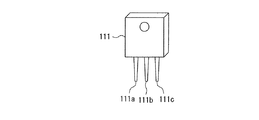
図8は、ディスクリート構成のIGBTの外観構成を示す斜視図である。
図8において、IGBT111は封止樹脂にて封止され、IGBT111のゲート端子111a、正側出力端子に接続されるコレクタ端子111bおよび負側出力端子に接続されるエミッタ端子111cが封止樹脂から取り出されている。
FIG. 8 is a perspective view showing an external configuration of a discrete IGBT.
In FIG. 8, the IGBT 111 is sealed with a sealing resin, and the
図9は、従来のIGBTの実装方法を示す斜視図、図10は、従来のIGBTの実装方法を示す断面図である。
図9および図10において、IGBT111にてインバータを構成する場合、IGBT111は、放熱のためにアース電位に接続されたヒートシンク123にねじ止めされる。例えば、三相インバータでは、上アーム用として3個、下アーム用として3個のIGBT111を1組として同一のヒートシンク123にねじ止めすることができる。
そして、ヒートシンク123にねじ止めされたIGBT111は、プリントパターン122が形成されたプリント基板121上に実装され、ゲート端子111a、コレクタ端子111bおよびエミッタ端子111cがプリントパターン122に接続される。
FIG. 9 is a perspective view showing a conventional IGBT mounting method, and FIG. 10 is a cross-sectional view showing a conventional IGBT mounting method.
9 and 10, when an inverter is constituted by the IGBT 111, the IGBT 111 is screwed to a
The IGBT 111 screwed to the
ここで、IGBT111を構成する半導体チップを出力端子と接続できるようにするために、IGBT111のパッケージ内部では半導体チップは金属パターン上に実装される。そして、IGBT111をヒートシンク123上に搭載すると、IGBT111のパッケージ内部の金属パターンとヒートシンク123とが対向するように配置されることから、IGBT111のコレクタとヒートシンク123との間に浮遊容量C122が形成される。
Here, in order to connect the semiconductor chip constituting the
また、ヒートシンク123にねじ止めされたIGBT111をプリント基板121上に実装すると、プリントパターン122とヒートシンク123とが対向するように配置されることから、プリントパターン122とヒートシンク123との間の静電結合によって浮遊容量C121が形成されるとともに、プリントパターン122が互いに近接して配置されると、プリントパターン122間にも浮遊容量が形成される。
Further, when the IGBT 111 screwed to the
すなわち、簡単のためにIGBT111の周辺の静電結合に限定して考えると、直流中間コンデンサの正極と上アーム用のIGBT111のコレクタを接続するプリントパターン122をパターンA、上アーム用のIGBT111のエミッタと下アーム用のIGBT111のコレクタを接続するプリントパターン122をパターンB、下アーム用のIGBT111のエミッタと直流中間コンデンサの負極を接続するプリントパターン122をパターンCとすると、プリントパターンA、B、Cとヒートシンク123との間、プリントパターンA、B間、プリントパターンB、C間、プリントパターンA、C間の静電結合によって浮遊容量が形成される。
That is, for the sake of simplicity, when considering only the electrostatic coupling around the IGBT 111, the printed
図11は、図7の2素子構成のインバータを用いた場合におけるコモンモード電流経路を示す図である。
図11において、インバータモジュールは、アース電位と同電位のヒートシンク105上に実装され、上アーム側コレクタとヒートシンク105との間および下アーム側コレクタとヒートシンク105との間に形成される浮遊容量C5、C6もアース電位に接続される。これらの浮遊容量C5、C6の充放電電流がコモンモード電流となり、このコモンモード電流は、浮遊容量C5、C6を通るコモンモード電流経路RCを介して主に流れる。同様に、プリントパターン122とヒートシンク123との間の浮遊容量C121の充放電電流がコモンモード電流となる。
FIG. 11 is a diagram showing a common mode current path when the inverter having the two-element configuration of FIG. 7 is used.
In FIG. 11, the inverter module is mounted on a
そして、伝導ノイズや放射ノイズの大きさはコモンモード電流の大きさに依存し、コモンモード電流の大きさは上下アーム接続点とアースとの間の浮遊容量に比例することから、上下アーム接続点とアースとの間の浮遊容量が大きくなるに従って、伝導ノイズや放射ノイズも大きくなる。
また、特許文献1には、電力変換回路から浮遊容量を介して流れる充放電電流によって発生する不要電磁波を、電力変換回路の半導体モジュール内の電流ループの面積を小さくすることで低く抑えられるようにするために、電力変換回路を構成する半導体モジュールに直流正側電位の出力電極、直流負側電位の出力電極および負荷と接続される出力電極のほかに、アース電位等と同電位となる出力電極を設けるとともに、これを、銅バーを介してアース電位と同電位の銅ベースへ接続する方法が開示されている。
The magnitude of conduction noise and radiation noise depends on the magnitude of the common mode current, and the magnitude of the common mode current is proportional to the stray capacitance between the upper and lower arm connection point and the ground. As the stray capacitance between the ground and the ground increases, the conduction noise and radiation noise also increase.
Patent Document 1 discloses that unnecessary electromagnetic waves generated by charging / discharging current flowing from the power conversion circuit through the stray capacitance can be suppressed to a low level by reducing the area of the current loop in the semiconductor module of the power conversion circuit. In addition to the output electrode connected to the DC positive potential output, the DC negative potential output electrode, and the load on the semiconductor module constituting the power conversion circuit, the output electrode having the same potential as the ground potential, etc. And a method of connecting it to a copper base having the same potential as the ground potential via a copper bar is disclosed.
しかしながら、従来のIGBT111の実装方法では、プリントパターン122とヒートシンク123とが対向するように配置される。このため、プリントパターン122とヒートシンク123との間の浮遊容量C121が増大し、コモンモード電流が増加することから、伝導ノイズや放射ノイズを増大させる要因となるという問題があった。
また、特許文献1に開示された方法では、コモンモード電流経路を小さくすることができるが、プリントパターン122とヒートシンク123との間の浮遊容量C121については考慮されていないため、コモンモード電流の大きさを低減することができないという問題があった。
そこで、本発明の目的は、半導体スイッチング素子の実装時のレイアウトに起因するコモンモード電流の増大を抑制することが可能な電力変換装置を提供することである。
However, in the
In the method disclosed in Patent Document 1, the common mode current path can be reduced. However, since the stray capacitance C121 between the printed
Accordingly, an object of the present invention is to provide a power conversion device capable of suppressing an increase in common mode current caused by a layout when a semiconductor switching element is mounted.
上述した課題を解決するために、請求項1記載の電力変換装置によれば、スイッチング動作を行う半導体スイッチング素子と、前記半導体スイッチング素子が表面側に実装されたプリント基板と、前記プリント基板の表面側に配置され、前記半導体スイッチング素子から発生する熱を放熱する導電体と、前記プリント基板の表面側に形成され、前記半導体スイッチング素子のスイッチング動作にて電位が変動しない端子に接続された第1プリントパターンと、前記プリント基板の裏面側に形成され、前記半導体スイッチング素子のスイッチング動作にて電位が変動する端子に接続された第2プリントパターンと、を備え、前記第2プリントパターンと前記導電体とが重なり合う領域が覆われるように前記第1プリントパターンを配置することを特徴とする。 In order to solve the above-described problem, according to the power conversion device of claim 1, a semiconductor switching element that performs a switching operation, a printed board on which the semiconductor switching element is mounted on a surface side, and a surface of the printed board And a conductor that dissipates heat generated from the semiconductor switching element, and a first conductor that is formed on the surface side of the printed circuit board and that is connected to a terminal whose potential does not vary during the switching operation of the semiconductor switching element. A printed pattern, and a second printed pattern formed on the back side of the printed circuit board and connected to a terminal whose potential is changed by a switching operation of the semiconductor switching element. The second printed pattern and the conductor placing the first printed pattern such areas bets overlap is covered And features.
これにより、プリントパターンと導電体とを重ねて配置した場合においても、プリントパターンと導電体との間に形成される浮遊容量を小さくすることが可能となる。このため、実装面積の増大を抑制しつつ、半導体スイッチング素子の実装時のレイアウトに起因するコモンモード電流の増大を抑制することが可能となり、伝導ノイズや放射ノイズを低減することができる。 As a result, even when the printed pattern and the conductor are arranged to overlap, the stray capacitance formed between the printed pattern and the conductor can be reduced. For this reason, it is possible to suppress an increase in common mode current due to the layout at the time of mounting the semiconductor switching element while suppressing an increase in mounting area, and it is possible to reduce conduction noise and radiation noise.
また、第2プリントパターンから導電体に到達する電気力線を第1プリントパターンにて遮蔽することができ、第2プリントパターンと導電体とを重ねて配置した場合においても、第2プリントパターンと導電体との間に形成される浮遊容量を小さくすることが可能となることから、実装面積の増大を抑制しつつ、半導体スイッチング素子の実装時のレイアウトに起因するコモンモード電流の増大を抑制することが可能となる。 In addition , the lines of electric force reaching the conductor from the second print pattern can be shielded by the first print pattern, and even when the second print pattern and the conductor are arranged in an overlapping manner, Since the stray capacitance formed between the conductors can be reduced, the increase in the common mode current due to the layout when mounting the semiconductor switching element is suppressed while the increase in the mounting area is suppressed. It becomes possible.
また、請求項2記載の電力変換装置によれば、前記第1プリントパターンと前記導電体とが重なり合う領域は、前記第2プリントパターンと前記導電体とが重なり合う領域よりも面積が大きいことを特徴とする。
これにより、第2プリントパターンから導電体に到達する電気力線を減らすことができ、第2プリントパターンと導電体との間に形成される浮遊容量を小さくすることが可能となることから、半導体スイッチング素子の実装時のレイアウトに起因するコモンモード電流の増大を抑制することが可能となる。
Further, according to the power converter according to claim 2, wherein the first printed pattern and the conductive region and overlap the body, characterized in that a larger area than the region with the second printed pattern and the conductor overlap And
As a result, the lines of electric force reaching the conductor from the second print pattern can be reduced, and the stray capacitance formed between the second print pattern and the conductor can be reduced. It is possible to suppress an increase in common mode current due to the layout when the switching element is mounted.
本発明に係る電力変換装置によれば、プリントパターンと導電体との間に形成される浮遊容量を小さくすることが可能となり、半導体スイッチング素子の実装時のレイアウトに起因するコモンモード電流の増大を抑制することが可能となることから、伝導ノイズや放射ノイズを低減することができる。 According to the power conversion device of the present invention, it is possible to reduce the stray capacitance formed between the printed pattern and the conductor, and to increase the common mode current due to the layout when the semiconductor switching element is mounted. Since it becomes possible to suppress, conduction noise and radiation noise can be reduced.
以下、本発明の実施形態に係る電力変換装置について図面を参照しながら説明する。
図1は、本発明に関連する第1実施形態に係る電力変換装置のIGBTの実装方法を示す断面図である。
図1において、IGBT14は、放熱のためにアース電位に接続されたヒートシンク13にねじ止めされている。例えば、三相インバータでは、上アーム用として3個、下アーム用として3個のIGBT14を1組として同一のヒートシンク13にねじ止めすることができる。
Hereinafter, a power converter according to an embodiment of the present invention will be described with reference to the drawings.
FIG. 1 is a cross-sectional view showing a method for mounting an IGBT of a power converter according to a first embodiment related to the present invention.
In FIG. 1, the
そして、ヒートシンク13にねじ止めされたIGBT14は、プリントパターン12が形成されたプリント基板11上に実装され、IGBT14のゲート端子、コレクタ端子およびエミッタ端子がプリントパターン12に接続される。
ここで、ヒートシンク13は、IGBT14のスイッチング動作にて電位が変動する端子に接続されたプリントパターン12と対向しない位置に配置することができる。例えば、IGBT14を用いて三相インバータを構成した場合、上下アーム接続点に接続されたプリントパターン12はヒートシンク13と対向しない位置に配置することができる。
The
Here, the
これにより、プリントパターン12とヒートシンク13とを離して配置することが可能となり、コンデンサの静電容量は電極面積および比誘電率に比例し、電極間距離に反比例することから、プリントパターン12とヒートシンク13との間に形成される浮遊容量C11を小さくすることが可能となる。このため、IGBT14の実装時のレイアウトに起因するコモンモード電流の増大を抑制することが可能となり、伝導ノイズや放射ノイズを低減することができる。
As a result, the printed
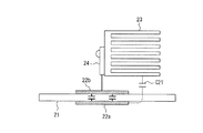
図2は、本発明の第2実施形態に係る電力変換装置のIGBTの実装方法を示す断面図である。
図2において、IGBT24は、放熱のためにアース電位に接続されたヒートシンク23にねじ止めされている。例えば、三相インバータでは、上アーム用として3個、下アーム用として3個のIGBT24を1組として同一のヒートシンク23にねじ止めすることができる。
FIG. 2 is a cross-sectional view illustrating a method for mounting an IGBT of a power conversion device according to a second embodiment of the present invention.
In FIG. 2, the
また、プリント基板21の表面には、プリントパターン22bが形成されるとともに、プリント基板21の裏面には、プリントパターン22bと対向するようにしてプリントパターン22aが形成されている。そして、ヒートシンク23にねじ止めされたIGBT24は、プリント基板21の表面側に実装され、IGBT24のスイッチング動作にて電位が変動しない端子はプリントパターン22bに接続されるとともに、IGBT24のスイッチング動作にて電位が変動する端子はプリントパターン22aに接続されている。なお、IGBT24のスイッチング動作にて電位が変動する端子をプリントパターン22aに接続する方法としては、例えば、プリント基板21に形成されたスルーホールを介して行うことができる。
A printed
例えば、IGBT24を用いて三相インバータを構成した場合、上下アーム接続点となる端子はプリントパターン22aに接続し、電力変換器の正極や負極に接続される端子はプリントパターン22bに接続することができる。ここで、プリントパターン22bはヒートシンク23との間で浮遊容量を形成した場合においても、IGBT24のスイッチング動作にて電位が変動しないことから、コモンモード電流が流れることはない。一方、プリントパターン22aと対向するようにしてプリントパターン22bを形成することにより、プリントパターン22a、22b間の静電結合を強めることができ、プリントパターン22aからヒートシンク23に到達する電気力線をプリントパターン22bにて遮蔽することができる。
For example, when a three-phase inverter is configured using the
これにより、プリントパターン22aとヒートシンク23とを重ねて配置した場合においても、プリントパターン22aとヒートシンク23との間に形成される浮遊容量C21を小さくすることが可能となることから、実装面積の増大を抑制しつつ、IGBT24の実装時のレイアウトに起因するコモンモード電流の増大を抑制することが可能となり、伝導ノイズや放射ノイズを低減することができる。
Thereby, even when the printed
図3は、本発明の第3実施形態に係る電力変換装置のIGBTの実装方法を示す断面図である。
図3において、IGBT34は、放熱のためにアース電位に接続されたヒートシンク33にねじ止めされている。例えば、三相インバータでは、上アーム用として3個、下アーム用として3個のIGBT34を1組として同一のヒートシンク33にねじ止めすることができる。
また、プリント基板31の表面には、プリントパターン32bが形成されるとともに、プリント基板31の裏面には、プリントパターン32aが形成されている。ここで、プリントパターン32bは、プリントパターン32aとヒートシンク33とが重なり合う領域が覆われるようにプリント基板31の表面に配置するとともに、プリントパターン32bに流れる電流を確保するための必要最小限の面積に設定することができる。
FIG. 3 is a cross-sectional view illustrating a method for mounting an IGBT of a power conversion device according to a third embodiment of the present invention.
In FIG. 3, the
A printed
そして、ヒートシンク33にねじ止めされたIGBT34は、プリント基板31の表面側に実装され、IGBT34のスイッチング動作にて電位が変動しない端子はプリントパターン32bに接続されるとともに、IGBT34のスイッチング動作にて電位が変動する端子はプリントパターン32aに接続されている。
例えば、IGBT34を用いて三相インバータを構成した場合、上下アーム接続点に接続される端子はプリントパターン32aに接続し、電力変換器の正極や負極に接続される端子はプリントパターン32bに接続することができる。ここで、プリントパターン32bはヒートシンク33との間で浮遊容量を形成した場合においても、IGBT34のスイッチング動作にて電位が変動しないことから、コモンモード電流が流れることはない。一方、プリントパターン32aと対向するようにしてプリントパターン32bを形成することにより、プリントパターン32a、32b間の静電結合を強めることができ、プリントパターン32aからヒートシンク33に到達する電気力線をプリントパターン22bにて遮蔽することができる。
The
For example, when a three-phase inverter is configured using the
これにより、プリントパターン32aとヒートシンク33とを重ねて配置した場合においても、プリントパターン32aとヒートシンク33との間に形成される浮遊容量C31を小さくすることが可能となり、実装面積の増大を抑制しつつ、IGBT34の実装時のレイアウトに起因するコモンモード電流の増大を抑制することが可能となる。
As a result, even when the
図4は、本発明の第4実施形態に係る電力変換装置のIGBTの実装方法を示す断面図である。
図4において、IGBT44は、放熱のためにアース電位に接続されたヒートシンク43にねじ止めされている。例えば、三相インバータでは、上アーム用として3個、下アーム用として3個のIGBT44を1組として同一のヒートシンク43にねじ止めすることができる。
FIG. 4 is a cross-sectional view illustrating an IGBT mounting method for a power conversion device according to a fourth embodiment of the present invention.
In FIG. 4, the
また、プリント基板41の表面には、プリントパターン42bが形成されるとともに、プリント基板41の裏面には、プリントパターン42aが形成されている。ここで、プリントパターン42bは、プリントパターン42aとヒートシンク43とが重なり合う領域が覆われるようにプリント基板41の表面に配置するとともに、プリントパターン42bとヒートシンク43とが重なり合う領域は、プリントパターン42aとヒートシンク43とが重なり合う領域よりも面積が大きくなるように設定することができる。そして、ヒートシンク43にねじ止めされたIGBT44は、プリント基板41の表面側に実装され、IGBT44のスイッチング動作にて電位が変動しない端子はプリントパターン42bに接続されるとともに、IGBT44のスイッチング動作にて電位が変動する端子はプリントパターン42aに接続されている。
A printed
例えば、IGBT44を用いて三相インバータを構成した場合、上下アーム接続点に接続される端子はプリントパターン42aに接続し、電力変換器の正極や負極に接続される端子はプリントパターン42bに接続することができる。ここで、プリントパターン42bはヒートシンク43との間で浮遊容量を形成した場合においても、IGBT44のスイッチング動作にて電位が変動しないことから、コモンモード電流が流れることはない。一方、プリントパターン42aと対向するようにしてプリントパターン42bを形成することにより、プリントパターン42a、42b間の静電結合を強めることができ、プリントパターン42aからヒートシンク43に到達する電束をプリントパターン42bにて遮蔽することができる。
For example, when a three-phase inverter is configured using the
これにより、プリントパターン42aとヒートシンク43とを重ねて配置した場合においても、プリントパターン42aからヒートシンク43に到達する電気力線を減らすことができ、プリントパターン42aとヒートシンク43との間に形成される浮遊容量C41を小さくすることが可能となることから、実装面積の増大を抑制しつつ、IGBT44の実装時のレイアウトに起因するコモンモード電流の増大を抑制することが可能となる。
As a result, even when the
図5は、本発明の第5実施形態に係る電力変換装置のIGBTの実装方法を示す断面図である。
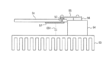
図5において、2in1タイプのIGBT54は、放熱のためにアース電位に接続されたヒートシンク53にねじ止めされている。また、プリント基板51の表面にはプリントパターン52が形成され、プリントパターン52はスルーホール57を介してプリント基板51の裏面に引き出されている。そして、IGBT54の出力端子に接続された電極56は、バスバー55を介してプリントパターン52に接続されている。
ここで、プリントパターン52は、IGBT54のスイッチング動作にて電位が変動する端子に接続することができ、例えば、IGBT54を用いて三相インバータを構成した場合、上下アーム接続点に接続することができる。
FIG. 5: is sectional drawing which shows the mounting method of IGBT of the power converter device which concerns on 5th Embodiment of this invention.
In FIG. 5, a 2-in-1
Here, the
また、プリントパターン52の面積が大きい場合、プリントパターン52はヒートシンク53と対向するように配置することができる。このような構成にするのは以下の理由からである。プリント基板はたかだか1〜2mm程度の厚さであるに対し、一般的に基板に使用されるFR4は比誘電率4〜5程度ある。基板の裏面にパターンをひくことで、浮遊容量の電極間距離が約1〜2mm長くなるが、基板比誘電率が大気(比誘電率1)より大きいために、静電容量が増加してしまう。したがって、別のプリントパターンによる遮蔽が困難な場合には、スイッチングにより激しく電位変動するパターンをヒートシンクに対向した位置に配置した方が、問題となる浮遊容量は小さく、漏れ電流は少なくなる。
When the area of the
ここで、ヒートシンク53と対向するようにプリントパターン52を配置する場合、プリントパターン52に流れる電流を確保するための必要最小限の面積に設定する。
これにより、プリントパターン52とヒートシンク53とが対向して配置された場合においても、プリントパターン52の面積を極力小さくすることが可能となることから、プリントパターン52とヒートシンク53との間に形成される浮遊容量C51を小さくすることが可能となる。このため、IGBT54の実装時のレイアウトに起因するコモンモード電流の増大を抑制することが可能となり、伝導ノイズや放射ノイズを低減することができる。
Here, when the
Thus, even when the
なお、上述した実施形態では、スイッチング素子としてIGBTを例にとって説明したが、パワーMOSFETやバイポーラトランジスタを用いるようにしてもよい。また、上述した実施形態では、ディスクリート構成のIGBTを用いて三相インバータを構成する方法を例にとって説明したが、本発明はインバータのアーム数や半導体の種類を問うことなく適用することができる。 In the above-described embodiment, the IGBT is described as an example of the switching element, but a power MOSFET or a bipolar transistor may be used. In the above-described embodiment, the method of configuring a three-phase inverter using discrete IGBTs has been described as an example. However, the present invention can be applied regardless of the number of arms of the inverter and the type of semiconductor.
さらに、上述した実施形態では、ヒートシンクがアースされている場合を例にとって説明したが、ヒートシンクがアースされてない場合に適用してもよい。
また、上述した実施形態では、スイッチングアームの直列回路で構成したインバータを例にとって説明したが、スイッチング素子が一つだけからなる電力変換装置に適用してもよい。
Furthermore, in the above-described embodiment, the case where the heat sink is grounded has been described as an example. However, the present invention may be applied when the heat sink is not grounded.
In the above-described embodiment, the inverter configured by a series circuit of switching arms has been described as an example. However, the present invention may be applied to a power conversion apparatus including only one switching element.
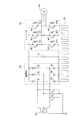
図6は、本発明の第6実施形態に係る電力変換装置の概略構成を回路的に示す図である。
図6において、フライバックコンバータでは、図11のスイッチング素子M11および帰還ダイオードD11の代わりに、トランス62の1次側が上アーム側に接続される。そして、トランス62の2次側には、ダイオードD61を介してコンデンサC61と抵抗R61との並列回路が接続されている。
FIG. 6 is a circuit diagram showing a schematic configuration of the power conversion device according to the sixth embodiment of the present invention.
In FIG. 6, in the flyback converter, the primary side of the
ここで、トランス62とスイッチング素子M14との接続点がプリントパターン61に接続されるものとすると、スイッチング素子M14の放熱に使われるヒートシンクは、プリントパターン61と対向しない位置に配置することができる。あるいは、スイッチング素子M14のスイッチング動作にて電位が変動しないプリントパターンをプリント基板の表面に形成するとともに、スイッチング素子M14のスイッチング動作にて電位が変動するプリントパターンをプリント基板の裏面に形成し、スイッチング素子M14の放熱に使われるヒートシンクをプリント基板の表面に配置するようにしてもよい。
Here, if the connection point between the
これにより、スイッチング素子が一つだけからなる電力変換装置に適用した場合においても、プリントパターン61とヒートシンクとの間に形成される浮遊容量を小さくすることが可能となり、スイッチング素子M14の実装時のレイアウトに起因するコモンモード電流の増大を抑制することが可能となる。
This makes it possible to reduce the stray capacitance formed between the printed
11、21、31、41、51…プリント基板
12、22a、22b、32a、32b、42a、42b、52…プリントパターン
13、23、33、43、53…ヒートシンク
14、24、34、44、54…IGBT
55…バスバー
56…電極
57…スルーホール
C11、C21、C31、C41、C51…浮遊容量
11, 21, 31, 41, 51 ... Printed
55 ...
Claims (2)
前記半導体スイッチング素子が表面側に実装されたプリント基板と、
前記プリント基板の表面側に配置され、前記半導体スイッチング素子から発生する熱を放熱する導電体と、
前記プリント基板の表面側に形成され、前記半導体スイッチング素子のスイッチング動作にて電位が変動しない端子に接続された第1プリントパターンと、
前記プリント基板の裏面側に形成され、前記半導体スイッチング素子のスイッチング動作にて電位が変動する端子に接続された第2プリントパターンと、を備え、
前記第2プリントパターンと前記導電体とが重なり合う領域が覆われるように前記第1プリントパターンを配置することを特徴とする電力変換装置。 A semiconductor switching element that performs a switching operation;
A printed circuit board on which the semiconductor switching element is mounted on the surface side;
A conductor disposed on the surface side of the printed circuit board and dissipating heat generated from the semiconductor switching element;
A first printed pattern formed on the surface side of the printed circuit board and connected to a terminal whose potential does not vary in the switching operation of the semiconductor switching element;
A second printed pattern formed on the back side of the printed circuit board and connected to a terminal whose potential varies in the switching operation of the semiconductor switching element ,
The power conversion device , wherein the first print pattern is arranged so as to cover a region where the second print pattern and the conductor overlap .
Priority Applications (1)
| Application Number | Priority Date | Filing Date | Title |
|---|---|---|---|
| JP2012059310A JP5516623B2 (en) | 2012-03-15 | 2012-03-15 | Power converter |
Applications Claiming Priority (1)
| Application Number | Priority Date | Filing Date | Title |
|---|---|---|---|
| JP2012059310A JP5516623B2 (en) | 2012-03-15 | 2012-03-15 | Power converter |
Related Parent Applications (1)
| Application Number | Title | Priority Date | Filing Date |
|---|---|---|---|
| JP2007070479A Division JP2008236855A (en) | 2007-03-19 | 2007-03-19 | Power conversion device |
Publications (2)
| Publication Number | Publication Date |
|---|---|
| JP2012110231A JP2012110231A (en) | 2012-06-07 |
| JP5516623B2 true JP5516623B2 (en) | 2014-06-11 |
Family
ID=46495184
Family Applications (1)
| Application Number | Title | Priority Date | Filing Date |
|---|---|---|---|
| JP2012059310A Expired - Fee Related JP5516623B2 (en) | 2012-03-15 | 2012-03-15 | Power converter |
Country Status (1)
| Country | Link |
|---|---|
| JP (1) | JP5516623B2 (en) |
Families Citing this family (2)
| Publication number | Priority date | Publication date | Assignee | Title |
|---|---|---|---|---|
| JP6433579B2 (en) * | 2015-04-07 | 2018-12-05 | 株式会社日立製作所 | Power converter |
| JP6880851B2 (en) | 2017-03-13 | 2021-06-02 | オムロン株式会社 | Power converter and power supply |
Family Cites Families (5)
| Publication number | Priority date | Publication date | Assignee | Title |
|---|---|---|---|---|
| JP2770652B2 (en) * | 1992-05-26 | 1998-07-02 | 富士通株式会社 | Switch element noise suppression method |
| JP2582144Y2 (en) * | 1992-10-16 | 1998-09-30 | 新電元工業株式会社 | Switching power supply circuit board |
| JPH11251525A (en) * | 1998-03-02 | 1999-09-17 | Toshiba Corp | Semiconductor device |
| JP2005197554A (en) * | 2004-01-09 | 2005-07-21 | Mitsubishi Electric Corp | Semiconductor device |
| JP2005310957A (en) * | 2004-04-20 | 2005-11-04 | Fujitsu Hitachi Plasma Display Ltd | Display unit |
-
2012
- 2012-03-15 JP JP2012059310A patent/JP5516623B2/en not_active Expired - Fee Related
Also Published As
| Publication number | Publication date |
|---|---|
| JP2012110231A (en) | 2012-06-07 |
Similar Documents
| Publication | Publication Date | Title |
|---|---|---|
| US10116201B2 (en) | High power density inverter (I) | |
| JP6041862B2 (en) | Power converter | |
| US8836080B2 (en) | Power semiconductor module | |
| US10811958B2 (en) | Water-cooling power supply module | |
| JP6041583B2 (en) | Power converter | |
| US10312801B2 (en) | High power density inverter (II) | |
| JP6206338B2 (en) | Switching module | |
| KR20190040194A (en) | Power semiconductor modules, snubber circuits, and induction heating power supplies | |
| JP2008042124A (en) | Semiconductor power module | |
| JP2006197735A (en) | Inverter | |
| JP4687414B2 (en) | Power semiconductor module | |
| JP4872345B2 (en) | Inverter module of power converter | |
| JP2005251839A (en) | Insulating substrate of power semiconductor module | |
| JP5516623B2 (en) | Power converter | |
| JP2006115649A (en) | Power converter | |
| JP2005020868A (en) | Power converting circuit | |
| JP2006060986A (en) | Conductor structure of power converter | |
| JP6289577B2 (en) | Power converter | |
| JP2006196721A (en) | Power semiconductor device | |
| JP2008236855A (en) | Power conversion device | |
| JP5119741B2 (en) | Switching module | |
| JP4487682B2 (en) | Capacitor and installation method | |
| JP2004007888A (en) | Power conversion circuit | |
| JP2013004683A (en) | Power converter of printed board | |
| CN110506384B (en) | Low inductance half-bridge power module |
Legal Events
| Date | Code | Title | Description |
|---|---|---|---|
| A621 | Written request for application examination |
Free format text: JAPANESE INTERMEDIATE CODE: A621 Effective date: 20120315 |
|
| A977 | Report on retrieval |
Free format text: JAPANESE INTERMEDIATE CODE: A971007 Effective date: 20130605 |
|
| A131 | Notification of reasons for refusal |
Free format text: JAPANESE INTERMEDIATE CODE: A131 Effective date: 20130618 |
|
| A521 | Written amendment |
Free format text: JAPANESE INTERMEDIATE CODE: A523 Effective date: 20130809 |
|
| A131 | Notification of reasons for refusal |
Free format text: JAPANESE INTERMEDIATE CODE: A131 Effective date: 20131105 |
|
| A521 | Written amendment |
Free format text: JAPANESE INTERMEDIATE CODE: A523 Effective date: 20131220 |
|
| TRDD | Decision of grant or rejection written | ||
| A01 | Written decision to grant a patent or to grant a registration (utility model) |
Free format text: JAPANESE INTERMEDIATE CODE: A01 Effective date: 20140304 |
|
| A61 | First payment of annual fees (during grant procedure) |
Free format text: JAPANESE INTERMEDIATE CODE: A61 Effective date: 20140317 |
|
| R150 | Certificate of patent or registration of utility model |
Ref document number: 5516623 Country of ref document: JP Free format text: JAPANESE INTERMEDIATE CODE: R150 |
|
| LAPS | Cancellation because of no payment of annual fees |