JP5515216B2 - Adaptive bandwidth phase-locked loop with feedforward divider. - Google Patents
Adaptive bandwidth phase-locked loop with feedforward divider. Download PDFInfo
- Publication number
- JP5515216B2 JP5515216B2 JP2007341739A JP2007341739A JP5515216B2 JP 5515216 B2 JP5515216 B2 JP 5515216B2 JP 2007341739 A JP2007341739 A JP 2007341739A JP 2007341739 A JP2007341739 A JP 2007341739A JP 5515216 B2 JP5515216 B2 JP 5515216B2
- Authority
- JP
- Japan
- Prior art keywords
- sub
- pll
- division ratio
- clock signal
- output
- Prior art date
- Legal status (The legal status is an assumption and is not a legal conclusion. Google has not performed a legal analysis and makes no representation as to the accuracy of the status listed.)
- Active
Links
Images
Classifications
-
- H—ELECTRICITY
- H03—ELECTRONIC CIRCUITRY
- H03L—AUTOMATIC CONTROL, STARTING, SYNCHRONISATION OR STABILISATION OF GENERATORS OF ELECTRONIC OSCILLATIONS OR PULSES
- H03L7/00—Automatic control of frequency or phase; Synchronisation
- H03L7/06—Automatic control of frequency or phase; Synchronisation using a reference signal applied to a frequency- or phase-locked loop
- H03L7/16—Indirect frequency synthesis, i.e. generating a desired one of a number of predetermined frequencies using a frequency- or phase-locked loop
- H03L7/22—Indirect frequency synthesis, i.e. generating a desired one of a number of predetermined frequencies using a frequency- or phase-locked loop using more than one loop
- H03L7/23—Indirect frequency synthesis, i.e. generating a desired one of a number of predetermined frequencies using a frequency- or phase-locked loop using more than one loop with pulse counters or frequency dividers
-
- H—ELECTRICITY
- H03—ELECTRONIC CIRCUITRY
- H03L—AUTOMATIC CONTROL, STARTING, SYNCHRONISATION OR STABILISATION OF GENERATORS OF ELECTRONIC OSCILLATIONS OR PULSES
- H03L7/00—Automatic control of frequency or phase; Synchronisation
- H03L7/06—Automatic control of frequency or phase; Synchronisation using a reference signal applied to a frequency- or phase-locked loop
- H03L7/08—Details of the phase-locked loop
- H03L7/085—Details of the phase-locked loop concerning mainly the frequency- or phase-detection arrangement including the filtering or amplification of its output signal
- H03L7/089—Details of the phase-locked loop concerning mainly the frequency- or phase-detection arrangement including the filtering or amplification of its output signal the phase or frequency detector generating up-down pulses
- H03L7/0891—Details of the phase-locked loop concerning mainly the frequency- or phase-detection arrangement including the filtering or amplification of its output signal the phase or frequency detector generating up-down pulses the up-down pulses controlling source and sink current generators, e.g. a charge pump
- H03L7/0895—Details of the current generators
-
- H—ELECTRICITY
- H03—ELECTRONIC CIRCUITRY
- H03L—AUTOMATIC CONTROL, STARTING, SYNCHRONISATION OR STABILISATION OF GENERATORS OF ELECTRONIC OSCILLATIONS OR PULSES
- H03L7/00—Automatic control of frequency or phase; Synchronisation
- H03L7/06—Automatic control of frequency or phase; Synchronisation using a reference signal applied to a frequency- or phase-locked loop
- H03L7/08—Details of the phase-locked loop
- H03L7/085—Details of the phase-locked loop concerning mainly the frequency- or phase-detection arrangement including the filtering or amplification of its output signal
- H03L7/093—Details of the phase-locked loop concerning mainly the frequency- or phase-detection arrangement including the filtering or amplification of its output signal using special filtering or amplification characteristics in the loop
-
- H—ELECTRICITY
- H03—ELECTRONIC CIRCUITRY
- H03L—AUTOMATIC CONTROL, STARTING, SYNCHRONISATION OR STABILISATION OF GENERATORS OF ELECTRONIC OSCILLATIONS OR PULSES
- H03L7/00—Automatic control of frequency or phase; Synchronisation
- H03L7/06—Automatic control of frequency or phase; Synchronisation using a reference signal applied to a frequency- or phase-locked loop
- H03L7/08—Details of the phase-locked loop
- H03L7/099—Details of the phase-locked loop concerning mainly the controlled oscillator of the loop
- H03L7/0995—Details of the phase-locked loop concerning mainly the controlled oscillator of the loop the oscillator comprising a ring oscillator
Landscapes
- Stabilization Of Oscillater, Synchronisation, Frequency Synthesizers (AREA)
Description
本発明の実施形態は、一般的に位相ロックループに関する。 Embodiments of the present invention generally relate to phase locked loops.
位相ロックループ(PLL)は、一般的に集積回路チップ及びシステムに使用され、入力信号に関連した周波数及び位相を有する規準信号と呼ばれる信号を発生させる。基準信号は、典型的にはクロック信号である。PLLの出力信号も、典型的には入力基準クロック信号に「固定した」クロック信号である。PLLは、マイクロプロセッサ、通信機器、及び他の電子機器を含む広範なチップにおいて使用される。 Phase locked loops (PLLs) are commonly used in integrated circuit chips and systems to generate a signal called a reference signal having a frequency and phase associated with an input signal. The reference signal is typically a clock signal. The output signal of the PLL is also a clock signal that is typically “fixed” to the input reference clock signal. PLLs are used in a wide range of chips including microprocessors, communication equipment, and other electronic equipment.
典型的なPLLは、位相周波数検出器(PFD)、チャージポンプ(CP)、ループフィルタ(LF)(ローパスフィルタとすることができる)、電圧制御発振器(VCO)、及び周波数分割回路を含む。PFDは、基準信号の位相を周波数分割回路からのフィードバック信号と比較する。基準信号及びフィードバック信号の位相関係により、PFDは、LFを通じてVCOへの電圧を昇圧又は降圧するようにCPに命令する信号をCPに供給する。LFは、信号を積分してそれを平滑化することができる。平滑化された信号は、VCOに供給される。VCOの周波数は、LFからの電圧信号に応じて高く又は低くなる。VCOの出力は、基準信号に比例して(又はそれに等しい)かつそれと同相の周波数をVCOの出力信号に持たせるループ内の周波数分割器を通じてPFDに返される。 A typical PLL includes a phase frequency detector (PFD), a charge pump (CP), a loop filter (LF) (which can be a low pass filter), a voltage controlled oscillator (VCO), and a frequency divider circuit. The PFD compares the phase of the reference signal with the feedback signal from the frequency division circuit. Depending on the phase relationship between the reference signal and the feedback signal, the PFD supplies the CP with a signal that instructs the CP to step up or step down the voltage to the VCO through the LF. The LF can integrate the signal and smooth it. The smoothed signal is supplied to the VCO. The frequency of the VCO increases or decreases depending on the voltage signal from the LF. The output of the VCO is returned to the PFD through a frequency divider in a loop that causes the VCO output signal to have a frequency in proportion to (or equal to) and in phase with the reference signal.
多くのPFDは、周波数の差に応答することができ、これは、許容入力のロックイン範囲を拡大させる。一部のPLLは、基準クロック信号と位相検出器への基準入力との間に分割回路を含む。一部の設計では、PFDの2つの出力があり、1つは、CPにVCOへの電圧を増加させるアップ信号を有し、別のものは、CPにVCOへの電圧を低下させるダウン信号を有する。
適応帯域幅PLLは、処理、電圧、及び温度(PVT)変動と殆ど無関係に作動周波数に比例してその力学をスケーリングするPLLの部類を意味する。
Many PFDs can respond to frequency differences, which increases the allowable input lock-in range. Some PLLs include a divider circuit between the reference clock signal and the reference input to the phase detector. In some designs, there are two outputs of the PFD, one has an up signal that increases the voltage to the VCO on the CP, and another has a down signal that decreases the voltage to the VCO on the CP. Have.
Adaptive bandwidth PLL refers to a class of PLLs that scale their dynamics in proportion to their operating frequency almost independent of processing, voltage, and temperature (PVT) variations.
アナログPLL設計者が今日直面している課題の1つは、リングVCO周波数範囲の減少である。VCO制御電圧の使用可能範囲は、供給電圧が1.2V(ボルト)よりも低くなったので相当に縮小した。一方、PLL適用領域は、拡大し続け、1つのPLLから更に広い周波数範囲を要求している。 One challenge facing analog PLL designers today is the reduction of the ring VCO frequency range. The usable range of the VCO control voltage was considerably reduced because the supply voltage was lower than 1.2V (volt). On the other hand, the PLL application area continues to expand and requires a wider frequency range from one PLL.
一部の実施形態では、チップは、第1及び第2の電圧制御式発振器(VCO)出力信号を供給するための第1及び第2のVCOと、第1及び第2VCO出力信号の第1及び第2の周波数を第1及び第2の分周率によって分割するための第1及び第2のフィードフォワード分割回路とを含む第1及び第2のサブ位相ロックループ(サブPLL)を含む。チップはまた、第1及び第2分周率を選択するための位相ロックループ制御回路を含む。 In some embodiments, the chip includes first and second VCOs for providing first and second voltage controlled oscillator (VCO) output signals, and first and second VCO output signal first and second VCO output signals. First and second sub-phase-locked loops (sub-PLLs) including first and second feed-forward dividing circuits for dividing the second frequency by the first and second division ratios are included. The chip also includes a phase locked loop control circuit for selecting the first and second division ratios.
一部の実施形態では、PLL制御回路は、第1及び第2出力クロック信号と第1及び第2VCO内への第1及び第2フィードフォワード電圧信号入力とに応答して第1及び第2分周率を選択する。
一部の実施形態では、方法は、第1及び第2サブ位相ロックループ(サブPLL)の第1及び第2電圧制御式発振器(VCO)に電圧制御信号を供給する段階を含む。更に、本方法は、第1及び第2VCOから第1及び第2VCO出力信号と第1及び第2フィードフォワード分割回路とを出力する段階と、第1及び第2VCO出力信号の第1及び第2周波数を第1及び第2分周率によって分割する段階と、第1及び第2分周率を選択する段階とを含む。
In some embodiments, the PLL control circuit is responsive to first and second output clock signals and first and second feedforward voltage signal inputs into the first and second VCOs. Select the frequency.
In some embodiments, the method includes providing a voltage control signal to first and second voltage controlled oscillators (VCOs) of first and second sub phase locked loops (sub PLLs). Further, the method includes outputting first and second VCO output signals and first and second feedforward divider circuits from the first and second VCOs, and first and second frequencies of the first and second VCO output signals. Are divided by the first and second division ratios, and the first and second division ratios are selected.
更に別の実施形態では、チップは、入力クロック信号を搬送する少なくとも1つの導体と、デュアル位相ロックループ(デュアルPLL)とを含む。デュアルPLLは、第1及び第2VCO出力信号を供給する第1及び第2電圧制御式発振器(VCO)と、第1及び第2分周率によって第1及び第2VCO出力信号の第1及び第2周波数を分割する第1及び第2フィードフォワード分割回路と含む第1及び第2サブ位相ロックループ(サブPLL)、及び第1及び第2分周率を選択する位相ロックループ制御回路を含む。
他の実施形態も説明して特許請求する。
本発明は、本発明の実施形態を示すために使用される以下の説明及び添付図面を参照することによって理解することができる。しかし、本発明は、これらの図面の詳細に限定されるものではない。
In yet another embodiment, the chip includes at least one conductor that carries an input clock signal and a dual phase locked loop (dual PLL). The dual PLL includes first and second voltage controlled oscillators (VCOs) that supply first and second VCO output signals, and first and second VCO output signals according to first and second division ratios. First and second sub-phase lock loops (sub-PLL) including first and second feed-forward division circuits for dividing the frequency, and a phase lock loop control circuit for selecting the first and second division ratios are included.
Other embodiments are also described and claimed.
The present invention can be understood by reference to the following description and attached drawings that are used to illustrate embodiments of the invention. However, the invention is not limited to the details of these drawings.
一部の実施形態では、本発明は、広い周波数範囲を有する適応帯域幅PLLを含む。単に例示的に、一部の実施形態では、周波数範囲は、500:1であるが、他の比率でもよい。一部の実施形態では、周波数範囲は、動的にフィードフォワード分割器の分周率を調節するデュアルPLLアーキテクチャにより拡大される。
図1は、位相周波数検出器(PFD)10と、チャージポンプ(CP)/ループフィルタ(LF)16と、電圧制御式発振器(VCO)22及び分周率Nを有するフィードフォワード周波数分割器(FF Div)24を含む出力周波数制御回路20と、分周率Mを有するフィードバック周波数分割器(FB Div)28とを有するPLL10を示している。VCO22は、周波数fVCOを有するVCO信号を供給する。「FF Div」24は、周波数fOUTを有する出力クロック信号(out clk)を供給し、かつこの信号はまた、「FB Div」28に対しても供給される。「FB Div」28の出力は、PFD14への入力として供給される。CP/LF16のチャージポンプ及びループフィルタは、異なる回路であるが、図示を容易にするために結合されている。「FF Div」24の分周率(N)は、調節される。一部の実施形態では、VCOの調節領域が比較的狭い場合であっても、この調節によって「FF Div」24が広い領域の周波数を発生させることを可能にする。
In some embodiments, the present invention includes an adaptive bandwidth PLL having a wide frequency range. By way of example only, in some embodiments, the frequency range is 500: 1, although other ratios may be used. In some embodiments, the frequency range is extended by a dual PLL architecture that dynamically adjusts the division ratio of the feedforward divider.
FIG. 1 illustrates a phase frequency detector (PFD) 10, a charge pump (CP) / loop filter (LF) 16, a voltage controlled oscillator (VCO) 22, and a feedforward frequency divider (
図2は、分周率Nの異なる値、例えば、N=24、N=23、N=22、N=21などに対するlogfVCO対logfOUTの線のグラフを示している。fVCOの周波数がfoとfo/2との間で高くなる時、fOUTの周波数は、N=24に対するfo/24を始点として、N=23に対するfo/23を始点として、N=22に対するfo/22を始点として、N=21に対するfo/21を始点として高くなる。1つの線(例えば、N=24の線)の最高周波数が、次の線(例えば、N=23の線)の最低周波数よりも高くなるように、周波数の線は、重なり合うことになることに注意されたい。 FIG. 2 shows a graph of the logf VCO vs. logf OUT line for different values of the division ratio N, for example, N = 2 4 , N = 2 3 , N = 2 2 , N = 2 1, etc. When the frequency of f VCO increases between fo and fo / 2, the frequency of f OUT as starting point fo / 2 4 for N = 2 4, the fo / 2 3 as the starting point for the N = 2 3, the fo / 2 2 for N = 2 2 as the starting point, the higher the fo / 2 1 for N = 2 1 as a starting point. The frequency lines will overlap so that the highest frequency of one line (eg, N = 2 4 line) is higher than the lowest frequency of the next line (eg, N = 2 3 line). Please note that.
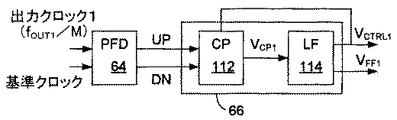
図3は、2つのPLL、サブPLL1、及びサブPLL2を含むデュアルPLL回路50を示し、各サブPLLは、図1のPLL10と同様である。サブPLL1において、PFD64は、基準クロック信号(ref clk)及び「out clk」1の周波数FOUT1をMによって分割するフィードバック周波数分割器78の出力を受け取る。PFD64は、CP/LF66に対して信号を供給し、CP/LF66は、電圧信号VCTRL1及び電圧信号VFF1を出力周波数制御回路70のVCO72に供給する。信号VCOclk1は、VCO72の出力であり、VCOclk1信号をN1によって分割するフィードフォワード周波数分割回路74に供給される。ここで、N1は、例えば図2及び4に示されている変数である。出力クロック信号(out clk 1)は、分割されたVCOclk1信号であり、この信号は、選択回路79に供給される。
FIG. 3 shows a
サブPLL2において、PFD84は、基準クロック信号(ref clk)及び「out clk」1の周波数fOUT2をMによって分割するフィードバック周波数分割器98の出力を受け取る。PFD84は、CP/LF86に信号を供給し、CP/LF86は、電圧信号VCTRL2及び電圧信号VFF2を出力周波数制御回路90のVCO92に供給する。信号VCOclk2は、VCO92の出力であり、VCOclk2信号をN2によって分割するフィードフォワード周波数分割回路94に供給される。ここで、N2は、例えば図2及び4に示されている変数である。出力クロック信号(out clk 2)は、分割されたVCOclk2信号であり、この信号は、選択回路79に供給される。
In
PLL制御回路82は、N1及びN2の値を選択し、選択回路79に選択信号を供給して、「out clk」1又は「out clk」2が出力信号として選択回路79によって供給されるか否かを制御する。一部の実施形態では、N1はN2に等しく、他の実施形態では、N1とN2は異なる場合がある。一部の実施形態では、PLL制御回路82は、VCTRL1及びVCTRL2並びに判断を助けるための出力クロック信号「out clk」1及び「out clk」2を受け取る。他の実施形態では、PLL制御回路82は、VCOxlk1及びVCOclk2信号を受け取る。
図3において、周波数範囲は、フィードフォワード分割回路74及び94を通して拡張することができる。低周波数fOUTが必要になる場合、分割器74及び94は、VCO72及び92を低fOUTで振動させる代わりに、N1又はN2によりVCO周波数(fVCO)を低下させる。上述のように、PLL制御回路82は、N1及びN2を選択する。一部の実施形態では、選択上の問題は、デジタル的に選択可能な負荷コンデンサを有するLC発振器において直面する粗周波数制御問題に類似している。従来方式は、VCO制御電圧(VCTRL)を外部から供給される上限と下限(VH及びVL)の間に設定するNを選択する段階を含む。しかし、リング発振器が、LC発振器よりもPVT変動に対して敏感であるので、この方式は、リング発振器に向いていないと考えられる。第1に、切れ目のない周波数のカバー範囲を保証するために、外部制限VH及びVLは、慎重にマージンを設定し、隣接周波数のサブ領域間に十分な重なりを補償することができる。第2に、Nを変化させることは、PLLに一時的に固定を失わせることになるので、Nの選択は、起動時に1回のみ行うことができ、十分なマージンを有するように慎重に行って、起こり得る最悪のPVT変動を少しずつ調節することができる。これらのマージンは、VCOの広範な調節範囲を必要とし、フィードフォワード分割回路74及び94の利点を減少する。
In FIG. 3, the frequency range can be extended through
提案するデュアルPLL回路(図3におけるような)は、Nを動的に変化させることを可能にし、かつVCTRLの中間レベルに設定するために単一の電圧VOPTを使用することにより、これらのマージンの必要性をなくすことができる。図3に表現したように、デュアルPLLは、異なるフィードフォワード分周率N1及びN2を有する2つのサブPLL1及びサブPLL2を含む。一方のサブPLLは、選択回路79を通して出力(out clk)を駆動すると共に、他方のサブPLLは、より良いNを検索する。後者がより良いNを見出した場合、後者は、出力を駆動する役割を引き継ぎ、前者は、新たなNの検索を開始する。固定したサブPLLのみが出力を駆動するので、Nの切り換えからの過渡状態は、出力から隠され、分周率Nを実時間で変更することができる。Nの最適性は、固定されたVCTRLのVOPTへの接近度によって評価され、従って、使用されるVCTRLの範囲は、VH及びVLを設定することなくVOPTに合わせられることになる。従って、以前の方式において必要とされた上述のマージンは、もはや必要とされない。更に、中間VCTRLレベルのVOPTを、VCOのPVT状態を追跡するように設計して、常にこれを最小ジッタに対して最適なVCTRL範囲に置くことができる。
The proposed dual PLL circuit (as in FIG. 3) allows these to be changed dynamically, and by using a single voltage V OPT to set it to an intermediate level of V CTRL The need for margins can be eliminated. As represented in FIG. 3, the dual PLL includes two sub-PLL1 and sub-PLL2 having different feedforward division ratios N1 and N2. One sub PLL drives the output (out clk) through the
図4は、N1及びN2を発見するためのアルゴリズムを示している。単に一例として、一部の実施形態では、1対のVCO分割器は、分周率Nが2のべき乗をとることを仮定して2:1の狭いfVCO範囲で広い範囲のfOUTを発生させるが、他の実施形態は、これらの詳細に限定されない。図4は、分周率Nの異なる値、例えば、N=26、N=25、N=24、N=23、N=22、N=21などに対する確定したfCTRL対logfOUTのグラフを示している。「確定した」は、PLLが確定するか又は固定されることを指す。図4には、3種の類似の直線がある。細い実線は、2偶数に等しいNの値に対するサブPLL1のVCTRL対fOUT特性を示している。細い破線は、2奇数に等しいNの値に対するサブPLL2のVCTRL対fOUT特性を示している。太い実線は、選択されたサブPLL(サブPLL1又はサブPLL2)のVCTRL対fOUT特性を示している。図2の場合と同様に、1つの線分の最高周波数が次の線分の最低周波数よりも大きくなるように、周波数線分は、重なり合うことができる。しかし、太線の上端(大きな黒丸)は、次の線分の最下端(小さい丸)の直上にある。例えば、N=24の線分の最下部の小さい丸は、N=25の太線の頂点(大きい丸)と同一のfOUT値を有する。
FIG. 4 shows an algorithm for finding N1 and N2. By way of example only, in some embodiments, a pair of VCO dividers generates a wide range of f OUT with a narrow f VCO range of 2: 1 assuming that the division ratio N is a power of two. However, other embodiments are not limited to these details. FIG. 4 shows the determined f CTRL pairs for different values of the division ratio N, such as N = 2 6 , N = 2 5 , N = 2 4 , N = 2 3 , N = 2 2 , N = 2 1, etc. A graph of logf OUT is shown. “Determined” refers to the PLL being established or fixed. In FIG. 4, there are three similar straight lines. The thin solid line shows the V CTRL vs. f OUT characteristic of
VOPTにより近い確定したVCTRLを有するサブPLLは、出力を駆動する。サブPLLの駆動は、2つのVCTRLがVOPTに等しい距離を有する時、すなわち、2つのサブPLLがfOUTを発生させるために最適値に等しい時に変更される。切り換えられると、出力位相は、静的位相オフセット中の偏差のためシフトすることがある。この位相シフトがチャタリングによって高周波数のジッタに変化することを防ぐために、ヒステリシスを加えることができる。また、両方のVCRTLがVOPTよりも高いか又は低い時、それらの一方は、VOPTから離れすぎていると考えられ、選択されていないサブPLLは、それをより近づけるように係数4によってNを更新することができる。PLL50の帯域幅は、fVCO/(N×M)に比例して変えることができる。ここで、N×Mは、分周率の合計である。VOPTの値を選択するための異なる方法がある。正確なVOPT値は重要ではない場合もあるが、周波数における不連続性は、回避されるべきである。これは、図4において、次の線分の下端(小さい丸)の直上にある太線の上端(大きい丸)の間にかなりの空間があってはならないことを意味する。
A sub PLL with a defined V CTRL closer to V OPT drives the output. The driving of the sub PLL is changed when the two V CTRLs have a distance equal to V OPT , that is, when the two sub PLLs are equal to the optimum value to generate f OUT . When switched, the output phase may shift due to deviations in the static phase offset. Hysteresis can be added to prevent this phase shift from changing to high frequency jitter due to chattering. Also, when both V CRTL are higher or lower than V OPT , one of them is considered too far from V OPT and the unselected sub-PLL is multiplied by a factor of 4 to make it closer. N can be updated. The bandwidth of the
一部の実施形態では、PLL制御回路82は、分周率の動的かつ欠陥なしのスイッチングを可能にする。一部の実施形態では、比較的狭い調節範囲を使用することにより、PLL50は、最良の状態中でのみVCOを作動させることによって低ジッタを達成することができる。また、分周率Nによって明示的に制御される回路帯域幅を用いて、PLL50は、以前の実現手段よりも正確な適応帯域幅力学を維持することができる。
In some embodiments, the
図5は、チャージポンプ112に対するアップ信号及びダウン信号の両方を供給するPFD64の実施形態を示している。図5において、図3のCP/LF66は、チャージポンプ(CP)112及びループフィルタ(LF)114を含む。図6、7、及び8は、チャージポンプ112、ループフィルタ114、及びVCO72の一部の実施形態の詳細を提供するが、他の実施形態は、これらの詳細を含まない。
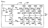
図6は、一部の実施形態によるチャージポンプ112及びそのバイアス回路の例を示すが、他の実施形態は、これらの詳細を含まない。適応式帯域幅に対してVBN(負バイアス)をVBNを通じてVCTRLに等しく設定することにより、チャージポンプ電流は、VCO電流に追従するようにバイアスされ、比較器122にフィードバック信号として供給される。また、このフィードバックは、VBP(正バイアス)を制御し、昇圧及び降圧電流が、例えば2%内に合わされて、静的位相オフセットを削減する。チャージポンプ112は、それぞれ、NMの1、2、及び4に対して、1倍、1/2倍、及び1/4倍の電流レベルをとるように区分される。Pチャンネル金属酸化膜半導体電界効果トランジスタ(PMOSFET)Q11、Q12、Q13、Q14、及びQ15のゲートは、比較器122の出力(VBP信号)を受け取ると共に、Nチャンネル金属酸化膜半導体電界効果トランジスタ(NMOSFET)Q26、Q27、Q28、Q29、及びQ30のゲートは、VBN信号を受け取る。「PMOSFET」Q17、Q18、Q19、及びQ20は、アップ信号UP0 *、UP1 *、UP2 *、及びUP2 *を受け取る。ここでUP0 *、UP1 *及びUP2 *は、UP0、UP1、及びUP2の論理的逆である。UP2は、UP0及びUP1の2倍の重みを有することに注意されたい。「NMOSFET」Q22、Q23、Q24、及びQ25は、ダウン信号DN0、DN1、DN2、及びDN3を受け取る。DN2は、DN0及びDN1の2倍の重みがあることに注意されたい。「PMOSFET」Q16及び「NMOSFET」Q21は、Q16及びQ21間にVBN信号を有してQ11及びQ26間で結合される。チャージポンプ電圧VCPは、「PMOSFET」Q17、Q18、Q19、及びQ20と「NMOSFET」Q22、Q23、Q24、及びQ25間に供給される。
FIG. 5 illustrates an embodiment of a
FIG. 6 illustrates an example of a
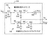
図7は、一部の実施形態によるループフィルタ114を示すが、他の実施形態は、これらの詳細を含まない。ループフィルタ114は、電荷再分配ネットワーク116及び半負荷サンプルフィードフォワードループフィルタ118を含む。電荷再分配116は、スイッチS1及びS1*(これはS1の逆である)を含む。スイッチS1及びS1*は、開及び閉であるかの2者択一である。コンデンサC11及びC12(それぞれ容量Cpを有する)は、それぞれ、接地とノードN11及びN12との間に結合される。バッファ112は、VCTRL信号を供給する。S1が閉であり、S1*が開である時、VCP及びVCTRL電圧は、ノード11上で統合され、C11中に蓄積される。各電荷再分配ネットワーク116は、ノード11においてVCP上に蓄積されるエラー電荷を半減することができる。プログラマブル分割器は、制御信号を発生し、スイッチを順に配列し、4よりも大きなN×Mに対してN×M/4(=2n+m-2)によってループ利得を縮小する。
FIG. 7 illustrates a
半負荷サンプルフィードフォワードループフィルタ118は、スイッチS2及びS2*(S2*は、S2の逆である)を含む。C13及びC14(それぞれ容量Cp及びC1を有する)は、それぞれ、接地とノードN13及びN14との間に結合される。ループフィルタ114は、基準サイクル長の半分であるフィードフォワードパルスVFFを生成し、基準周波数fREFとの望ましい比較を達成する。スイッチS1、S1*、S2、及びS2*は、コンデンサC11、C12、C13、及びC14上の電荷を制御するために開閉する。S1が閉じている時、C11上に蓄積された電荷は、C12と共有され、また、S2が閉じられている時、C11上の電荷は、C13と共有される。スイッチS1*は、C12上の電圧をリセットする。スイッチS1、S1*、S2、及びS2*は、図8のVCO回路からの出力を受け取る論理によって制御される。
The half-load sample feedforward loop filter 118 includes switches S2 and S2 * (S2 * is the inverse of S2). C13 and C14 (with capacitors Cp and C1, respectively) are coupled between ground and nodes N13 and N14, respectively. The
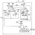
図8は、レプリカ補償電源レギュレータ(「PMOSFET」Q62及びQ64並びに「NMOSFET」Q63及びQ65を含む)を含むインバータベースのリング発振器を示している。レプリカフィードバックは、電源ノイズに応答する高速フィードバックパスを達成することによって電源ノイズ除去を改善する。ループフィルタ114からのフィードフォワード電圧VFFは、「NMOSFET」Q44及びQ47のゲートによって受け取られる。VFFが「high」(高い電圧を有する)の時、Q44及びQ47は、ONになり、Q42のドレーンを引き下げる。レギュレータ電圧VREGが「high」の時、「NMOSFET」Q43もまた、「PMOSFET」Q41のドレーン上で引き下げられ、「PMOSFET」Q41及びQ42をONにする。Q44、Q47、Q42がONの時、ノードN15は、「low」に引き下げられ、「PMOSFET」Q61をONにする。Q61のドレーンにおける電圧VRPL(レプリカ)は、「NMOSFET」Q46をONにする。「NMOSFET」Q45及びQ48のゲートは、VBN信号を受け取る。これは、図6に示すもの又は図6と同様な付加回路と同一の信号からのものであり、図8のVBNを発生する。
N15の電圧が引き下げられる時、「PMOSFET」Q71はONになり、VREGを昇圧してQ43をOFFにする。コンデンサC20は、電圧変動を平滑化する。電圧VREGは、インバータI1、I2、I3、I4、及びI5が振動する速度を制御し、その結果インバータI5から供給されるVCO1クロック信号の周波数を制御する。
FIG. 8 shows an inverter-based ring oscillator including replica compensated power supply regulators (including “PMOSFETs” Q62 and Q64 and “NMOSFETs” Q63 and Q65). Replica feedback improves power supply noise rejection by achieving a fast feedback path that is responsive to power supply noise. The feedforward voltage V FF from the
When the voltage at N15 is lowered, the “PMOSFET” Q71 is turned on, boosting V REG and turning off Q43. The capacitor C20 smoothes voltage fluctuation. The voltage V REG controls the speed at which the inverters I1, I2, I3, I4, and I5 oscillate, and as a result controls the frequency of the VCO1 clock signal supplied from the inverter I5.
図9は、サンプルチップ200における回路レイアウトを示している。PLL1は、LF、分割器(DIV)、PFD、CP、及びVCOを含む。PLL2は、同一の構成要素を含む。試験回路202は、PLL1及びPLL2を試験する。走査チェーン204は、PLLの一部にアクセスする外部回路を提供する。適応帯域PLLは、0.13μmCMOS処理で実施され、以下の特性を有していた。
処理技術:0.13μm、N−ウェル、1P6M CMOS
面積:1.1×0.46mm2
電源電圧:1.2V公称
ワット損:36mW
基準周波数範囲:2MHz〜1GHz
出力周波数範囲:2MHz〜1GHz
増倍率範囲:M=20〜9
ループ帯域幅:基準周波数の〜1/100
ジッタ(M=1、1.024GHz):13.10ps、pp、1.62ps、rms
FIG. 9 shows a circuit layout in the
Processing technology: 0.13 μm, N-well, 1P6M CMOS
Area: 1.1 × 0.46mm 2
Power supply voltage: 1.2V nominal Power dissipation: 36mW
Reference frequency range: 2 MHz to 1 GHz
Output frequency range: 2 MHz to 1 GHz
Gain range: M = 2 0-9
Loop bandwidth: ~ 1/100 of the reference frequency
Jitter (M = 1, 1.024 GHz): 13.10 ps, pp, 1.62 ps, rms
この例では、PLLは、広いN選択範囲21〜24を有していたが、この例示的PLLは、2MHzから1GHzの基準周波数範囲に固定されていた。チャージポンプにおける閾値下の漏れが、2MHzよりも低く作動を制限した可能性がある。Nの動的選択は、成功裏に行われ、VCO振動周波数は、1〜2GHzの狭い範囲に限定された。このPLLは、M×fREFが1GHzを超えない限り、M=2mを有するあらゆる逓倍周波数を供給することができると考えられる。測定されたジッタ対基準信号fREF及びMは、PLL帯域幅がfREFで縮小することを確認した。VCO位相ノイズが測定の設定では出力ジッタを支配していたので、追跡ジッタは、帯域幅の減少に伴い増加した。fOUTにNを自己適応させることにより、デュアルPLLアーキテクチャは、VCOをジッタ傾向の低周波数振動に近づけないようにし、その結果、固定NのPLLよりも低いジッタを達成する。ジッタ傾向における不連続点は、Nが切り換わる点を示し、静的位相オフセットにおける最悪ステップ変動は、基準サイクルの3.6%であった。本発明の他の実施では、上記と異なる詳細を含むことができることに注意されたい。
図10は、デュアルPLL234が外部クロック信号を受け取り、このデュアルPLLが回路238に内部クロック信号を供給するチップ230を示している。
In this example, the PLL had a wide N selection range 21-24 , but this exemplary PLL was fixed to a reference frequency range of 2 MHz to 1 GHz. A subthreshold leak in the charge pump may have limited operation below 2 MHz. The dynamic selection of N was successful and the VCO oscillation frequency was limited to a narrow range of 1-2 GHz. It is believed that this PLL can supply any multiplying frequency with M = 2 m as long as M × f REF does not exceed 1 GHz. The measured jitter versus reference signals f REF and M confirmed that the PLL bandwidth was reduced by f REF . Since VCO phase noise dominates the output jitter in the measurement setup, the tracking jitter increased with decreasing bandwidth. By self-adapting N to f OUT , the dual PLL architecture keeps the VCO close to jitter-prone low frequency oscillations, resulting in lower jitter than a fixed N PLL. The discontinuity in the jitter trend indicates the point where N switches, and the worst step variation in static phase offset was 3.6% of the reference cycle. It should be noted that other implementations of the invention may include details different from those described above.
FIG. 10 shows a
本発明は、いかなる特定の信号伝達形式にも限定されない。入力及びクロック信号は、シングルエンド又は区別したものとすることができる。クロッキングは、1倍データ転送速度、2倍データ転送速度、4倍データ転送速度などとすることができる。2倍データ転送速度では、単一のクロック信号の立ち上がり立下りエッジを使用することができ、又は位相クロックからの2つを使用することができる。信号は、パケット化又は非パケット化することができる。 The present invention is not limited to any particular signaling format. Input and clock signals can be single-ended or distinct. Clocking can be 1x data transfer rate, 2x data transfer rate, 4x data transfer rate, and the like. At double data rates, the rising and falling edges of a single clock signal can be used, or two from the phase clock can be used. The signal can be packetized or non-packetized.
本発明の開示は、本質的に概要であって様々な詳細を含まない様々な図を含む。実際の実施においては、システム及びチップは、示されてはいないが、図の回路間に含まれる付加的な構成要素を含むであろう。図示の構成要素は、様々な付加的な入力及び出力を有することができる。本明細書に説明した様々なアルゴリズム及び方法は、ファームウエア又はソフトウエアの支援なしにハードウエア回路中で実行することができる。しかし、ファームウエア及び/又はソフトウエアは、アルゴリズム及び方法が実行される全体的システムに使用することができる。
図3では、分割Mは、回路78及び98に対して同じであるが、これらは異なっていてもよい。
The present disclosure includes various figures that are schematic in nature and do not contain various details. In actual implementation, the system and chip will include additional components that are not shown, but are included between the illustrated circuits. The illustrated components can have a variety of additional inputs and outputs. The various algorithms and methods described herein can be implemented in hardware circuits without firmware or software assistance. However, firmware and / or software can be used for the overall system in which the algorithms and methods are executed.
In FIG. 3, the division M is the same for
本明細書で使用される場合、用語「実施形態」は、実施例を指す。「実施形態」、「一実施形態」、「一部の実施形態」、又は「他の実施形態」への本明細書中での参照は、これらの実施形態に関連して説明される特定の特徴、構造、又は特性が少なくとも一部の実施形態に含まれるが、本発明の全ての実施形態に含まれる必要はないことを意味する。「一部の実施形態」への異なる参照は、同じ「一部の実施形態」を指す必要はない。 As used herein, the term “embodiment” refers to an example. References herein to “embodiments”, “one embodiment”, “some embodiments”, or “other embodiments” are specific to the embodiments described in connection with these embodiments. It means that a feature, structure, or characteristic is included in at least some embodiments, but need not be included in all embodiments of the invention. Different references to “some embodiments” need not refer to the same “some embodiments”.
本明細書が、構成要素、特徴、構造、又は特性を含む「場合がある」、「かもしれない」、又は「ことができると考えられる」と説明する場合、この特定の構成要素、特徴、構造、又は特性は含まれる必要はない。本明細書又は特許請求の範囲が「a」を付した構造を参照する場合、これは、構造が1つのみであることを意味しない。
本発明をいくつかの実施形態によって説明したが、本発明は、説明したそれらの実施形態に限定されるべきではなく、特許請求の範囲及び精神の範囲内で修正及び変更して実施することができる。以上の説明は、従って、限定的ではなく例示的であるとみなすものとする。
Where this specification describes “may be”, “may be”, or “conceivable” to include a component, feature, structure, or characteristic, this particular component, feature, A structure or property need not be included. Where this specification or claim refers to structures with an “a”, this does not mean there is only one structure.
Although the invention has been described in terms of several embodiments, the invention should not be limited to those described embodiments, but can be practiced with modification and alteration within the scope and spirit of the claims. it can. The above description is therefore to be regarded as illustrative instead of limiting.
10 位相ロックループ
22 電圧制御式発振器
24 フィードフォワード周波数分割器
N、M 分周率
10 Phase Locked
Claims (14)
前記第1及び第2の分周率を選択し、前記第1のサブPLLからの前記第1の出力クロック信号又は前記第2のサブPLLからの前記第2の出力クロック信号のいずれかを出力信号として選択する位相ロックループ(PLL)制御回路であって、前記第1の出力クロック信号、前記第2の出力クロック信号、前記第1のサブPLLの前記第1のVCOによって受信される第1の制御電圧及び前記第2のサブPLLの前記第2のVCOによって受信される第2の制御電圧に基づいて、可変の分周率の選択と前記出力信号の選択をするPLL制御回路と、
を含み、
前記サブPLLの1つが、前記出力信号を提供するために前記位相ロックループ制御回路によって選択され、前記位相ロックループ制御回路が他のサブPLLに対する分周率を変更でき、
前記PLL制御回路による前記第1の分周率及び前記第2の分周率の選択は、前記第1の制御電圧及び前記第2の制御電圧が単一の最適電圧値に対してどの程度近いかに基づいていることを特徴とする位相ロックループ出力信号を生成するチップ。 First and second sub-phase locked loops (sub-PLLs) for supplying first and second voltage controlled oscillator (VCO) output signals; The first and second frequencies of the two VCO output signals are divided by variable first and second frequency division ratios to generate a first output clock signal from the first sub-PLL; First and second sub-phase-locked loops (sub-PLLs) including first and second feedforward divider circuits that generate a second output clock signal from the sub-PLL;
The first and second frequency division ratios are selected and either the first output clock signal from the first sub PLL or the second output clock signal from the second sub PLL is output. A phase-locked loop (PLL) control circuit to select as a signal , the first output clock signal, the second output clock signal, and a first VCO received by the first VCO of the first sub-PLL A PLL control circuit for selecting a variable division ratio and selecting the output signal based on the control voltage of the second sub-PLL and the second control voltage received by the second VCO of the second sub-PLL ;
Including
One of the sub-PLLs is selected by the phase-locked loop control circuit to provide the output signal, and the phase-locked loop control circuit can change the division ratio for the other sub-PLLs ;
The selection of the first division ratio and the second division ratio by the PLL control circuit is based on how close the first control voltage and the second control voltage are to a single optimum voltage value. A chip that generates a phase-locked loop output signal characterized by how it is based .
前記第1の分周率に対する前記整数は、前記第2の分周率に対する前記整数と異なっている、
ことを特徴とする請求項1に記載のチップ。 The first division ratio is equal to an integer power of 2, and the second division ratio is also equal to an integer power of 2.
The integer for the first division ratio is different from the integer for the second division ratio;
The chip according to claim 1.
第1及び第2の位相周波数検出器、及び
前記第1及び第2の出力クロック信号の前記周波数を分割する第1及び第2のフィードバック分割回路であって、第1及び第2の分割回路の出力を前記第1及び第2の位相周波数検出器に供給する第1及び第2のフィードバック分割回路、
を含む、
ことを特徴とする請求項1に記載のチップ。 The first and second sub PLLs are:
First and second phase frequency detectors, and first and second feedback divider circuits for dividing the frequencies of the first and second output clock signals, wherein the first and second divider circuits First and second feedback divider circuits that provide outputs to the first and second phase frequency detectors;
including,
The chip according to claim 1.
前記第1及び第2のVCOから第1及び第2のフィードフォワード分割回路に第1及び第2のVCO出力信号を出力する段階と、
前記第1のサブPLLから第1の出力クロック信号を生成すると共に前記第2のサブPLLから第2の出力クロック信号を生成するために、前記第1及び第2のフィードフォワード分割回路を用いて前記第1及び第2のVCO出力信号の第1及び第2の周波数を可変の第1及び第2の分周率によって分割する段階と、
前記第1及び第2分周率を選択する段階と、
記第1のサブPLLからの前記第1の出力クロック信号又は前記第2のサブPLLからの前記第2の出力クロック信号のいずれかを出力信号として選択する段階と、
を含み、
前記サブPLLの1つの前記出力クロック信号が、前記出力信号として選択され、他のサブPLLに対する分周率を変更でき、
前記可変の第1及び第2の分周率の選択と前記出力信号の選択は、前記第1の出力クロック信号、前記第2の出力クロック信号、前記第1のサブPLLの前記第1のVCOによって受信される第1の制御電圧及び前記第2のサブPLLの前記第2のVCOによって受信される第2の制御電圧に基づいてなされるものであり、前記PLL制御回路による前記第1の分周率及び前記第2の分周率の選択は、前記第1の制御電圧及び前記第2の制御電圧が単一の最適電圧値に対してどの程度近いかに基づいていることを特徴とする位相ロックループ出力信号を生成する方法。 Providing first and second voltage control signals to first and second voltage controlled oscillators (VCOs) of first and second sub phase locked loops (sub PLLs);
Outputting first and second VCO output signals from the first and second VCOs to first and second feedforward divider circuits;
In order to generate a first output clock signal from the first sub-PLL and a second output clock signal from the second sub-PLL, the first and second feedforward divider circuits are used. Dividing the first and second frequencies of the first and second VCO output signals by variable first and second division ratios;
Selecting the first and second division ratios;
Selecting either the first output clock signal from the first sub-PLL or the second output clock signal from the second sub-PLL as an output signal;
Including
The output clock signal of one of the sub PLLs is selected as the output signal, and the division ratio for the other sub PLLs can be changed .
The selection of the variable first and second frequency division ratios and the selection of the output signal are performed by selecting the first output clock signal, the second output clock signal, and the first VCO of the first sub PLL. Based on the first control voltage received by the second sub-PLL and the second control voltage received by the second VCO of the second sub-PLL. The selection of the divide ratio and the second divide ratio is based on how close the first control voltage and the second control voltage are to a single optimum voltage value. A method for generating a lock loop output signal.
第1及び第2の電圧制御式発振器(VCO)出力信号を供給する第1及び第2のVCOと、該第1及び第2のVCO出力信号の第1及び第2の周波数を可変の第1及び第2の分周率によって分割する第1及び第2のフィードフォワード分割回路とを含む第1及び第2のサブ位相ロックループ(サブPLL)であって、前記第1のサブPLLから第1の出力クロック信号を生成し、前記第2のサブPLLから第2の出力クロック信号を生成する第1及び第2のサブPLL、及び
前記第1及び第2の分周率を選択し、記第1のサブPLLからの前記第1の出力クロック信号又は前記第2のサブPLLからの前記第2の出力クロック信号のいずれかを出力信号として選択する位相ロックループ(PLL)制御回路、
を含むデュアル位相ロックループ(デュアルPLL)と、
を含み、
前記サブPLLの1つが、前記出力信号を提供するために前記PLL制御回路によって選択される一方で、前記PLL制御回路が他のサブPLLに対する分周率を変更でき、
前記可変の第1及び第2の分周率の選択と前記出力信号の選択は、前記第1の出力クロック信号、前記第2の出力クロック信号、前記第1のサブPLLの前記第1のVCOによって受信される第1の制御電圧及び前記第2のサブPLLの前記第2のVCOによって受信される第2の制御電圧に基づいてなされるものであり、前記PLL制御回路による前記第1の分周率及び前記第2の分周率の選択は、前記第1の制御電圧及び前記第2の制御電圧が単一の最適電圧値に対してどの程度近いかに基づいていることを特徴とする位相ロックループ出力信号を生成するチップ。 At least one conductor carrying an input clock signal;
First and second VCOs that supply first and second voltage controlled oscillator (VCO) output signals, and first and second frequencies of the first and second VCO output signals that are variable . And a first and second sub-phase locked loop (sub-PLL) including first and second feed-forward division circuits that divide by a second frequency division ratio, the first sub-PLL to the first sub-PLL The first and second sub PLLs that generate the second output clock signal from the second sub PLL, and the first and second frequency division ratios are selected, and A phase-locked loop (PLL) control circuit that selects either the first output clock signal from one sub-PLL or the second output clock signal from the second sub-PLL as an output signal;
Including a dual phase lock loop (dual PLL);
Including
One of the sub-PLLs is selected by the PLL control circuit to provide the output signal, while the PLL control circuit can change the division ratio for other sub-PLLs ;
The selection of the variable first and second frequency division ratios and the selection of the output signal are performed by selecting the first output clock signal, the second output clock signal, and the first VCO of the first sub PLL. Based on the first control voltage received by the second sub-PLL and the second control voltage received by the second VCO of the second sub-PLL. The selection of the divide ratio and the second divide ratio is based on how close the first control voltage and the second control voltage are to a single optimum voltage value. A chip that generates a lock loop output signal.
前記第1の分周率に対する前記整数は、前記第2の分周率に対する前記整数と異なっている、
ことを特徴とする請求項10に記載のチップ。 The first division ratio is equal to an integer power of 2, and the second division ratio is also equal to an integer power of 2.
The integer for the first division ratio is different from the integer for the second division ratio;
The chip according to claim 10 .
Applications Claiming Priority (2)
| Application Number | Priority Date | Filing Date | Title |
|---|---|---|---|
| US11/637,254 | 2006-12-11 | ||
| US11/637,254 US7602253B2 (en) | 2006-12-11 | 2006-12-11 | Adaptive bandwidth phase locked loop with feedforward divider |
Publications (2)
| Publication Number | Publication Date |
|---|---|
| JP2008148346A JP2008148346A (en) | 2008-06-26 |
| JP5515216B2 true JP5515216B2 (en) | 2014-06-11 |
Family
ID=38996611
Family Applications (1)
| Application Number | Title | Priority Date | Filing Date |
|---|---|---|---|
| JP2007341739A Active JP5515216B2 (en) | 2006-12-11 | 2007-12-11 | Adaptive bandwidth phase-locked loop with feedforward divider. |
Country Status (7)
| Country | Link |
|---|---|
| US (1) | US7602253B2 (en) |
| EP (1) | EP1933464B1 (en) |
| JP (1) | JP5515216B2 (en) |
| KR (1) | KR101470990B1 (en) |
| CN (1) | CN101202546B (en) |
| DE (1) | DE602007009176D1 (en) |
| TW (1) | TWI356592B (en) |
Families Citing this family (18)
| Publication number | Priority date | Publication date | Assignee | Title |
|---|---|---|---|---|
| US7747237B2 (en) * | 2004-04-09 | 2010-06-29 | Skyworks Solutions, Inc. | High agility frequency synthesizer phase-locked loop |
| US20080317185A1 (en) * | 2007-06-25 | 2008-12-25 | Broadcom Corporation | Dual phase locked loop (pll) architecture for multi-mode operation in communication systems |
| US7821343B1 (en) * | 2008-08-27 | 2010-10-26 | Altera Corporation | Transmitter with multiple phase locked loops |
| TWI384761B (en) * | 2009-02-20 | 2013-02-01 | Sunplus Technology Co Ltd | Low jitter, wide operating frequency band and frequency synthesis system suitable for low voltage operation |
| US8044726B2 (en) * | 2009-03-17 | 2011-10-25 | Qualcomm Incorporated | Systems and methods for self testing a voltage controlled oscillator |
| US7973612B2 (en) * | 2009-04-26 | 2011-07-05 | Qualcomm Incorporated | Supply-regulated phase-locked loop (PLL) and method of using |
| JP2011188077A (en) * | 2010-03-05 | 2011-09-22 | Renesas Electronics Corp | Phase locked loop circuit and control method thereof |
| US8415999B2 (en) | 2010-07-28 | 2013-04-09 | International Business Machines Corporation | High frequency quadrature PLL circuit and method |
| US8258835B1 (en) * | 2011-06-15 | 2012-09-04 | Asahi Kasei Microdevices Corporation | Cancellation system for phase jumps at loop gain changes in fractional-N frequency synthesizers |
| CN103269220A (en) * | 2013-05-30 | 2013-08-28 | 上海坤锐电子科技有限公司 | Clock recovery circuit through NFC active load modulation based on digital phase-locked loop |
| CN103346784B (en) * | 2013-06-18 | 2016-04-13 | 成都嘉纳海威科技有限责任公司 | A kind of matching type charge pump circuit for phase-locked loop |
| US9350362B2 (en) | 2013-10-08 | 2016-05-24 | Thomas & Betts International, Llc | Programmable slew rate phase locked loop |
| US9444473B2 (en) * | 2014-09-09 | 2016-09-13 | Qualcomm Incorporated | Increased synthesizer performance in carrier aggregation/multiple-input, multiple-output systems |
| ES2719545T3 (en) | 2015-04-15 | 2019-07-11 | Mitsubishi Electric Corp | Synthesizer |
| US10958278B2 (en) * | 2019-07-31 | 2021-03-23 | Intel Corporation | Techniques in phase-lock loop configuration in a computing device |
| JP7643994B2 (en) * | 2021-12-22 | 2025-03-11 | ルネサスエレクトロニクス株式会社 | Semiconductor Device |
| US12531564B2 (en) * | 2022-09-19 | 2026-01-20 | Qualcomm Incorporated | Synchronizing multiple phase-locked loop circuits |
| US12261609B1 (en) * | 2023-10-18 | 2025-03-25 | Shaoxing Yuanfang Semiconductor Co., Ltd. | Inter-PLL communication in a multi-PLL environment |
Family Cites Families (27)
| Publication number | Priority date | Publication date | Assignee | Title |
|---|---|---|---|---|
| JPS60197015A (en) | 1984-03-21 | 1985-10-05 | Nec Corp | Phase locked oscillator |
| JPS63305619A (en) * | 1987-06-08 | 1988-12-13 | Mitsubishi Electric Corp | Pll synthesizer device |
| JPH01120133U (en) * | 1988-02-06 | 1989-08-15 | ||
| JPH03190428A (en) * | 1989-12-20 | 1991-08-20 | Matsushita Electric Ind Co Ltd | Phase synchronizing circuit |
| JPH05145413A (en) * | 1991-11-20 | 1993-06-11 | Nippon Denki Musen Denshi Kk | Phase locked loop circuit |
| JPH05199109A (en) * | 1992-01-20 | 1993-08-06 | Ricoh Co Ltd | PLL circuit |
| JPH05227024A (en) * | 1992-02-12 | 1993-09-03 | Sony Tektronix Corp | Pll oscillation device |
| US5483202A (en) * | 1994-08-31 | 1996-01-09 | Polaroid Corporation | Compensated phase locked loop for generating a controlled output clock signal |
| JPH08125529A (en) * | 1994-10-20 | 1996-05-17 | Fujitsu General Ltd | PLL circuit |
| GB2295930B (en) | 1994-12-06 | 1999-11-24 | Motorola Ltd | Method and apparatus for implementing frequency hopping in a TDMA system |
| US5610558A (en) * | 1995-11-03 | 1997-03-11 | Motorola, Inc. | Controlled tracking of oscillators in a circuit with multiple frequency sensitive elements |
| JPH10271002A (en) * | 1997-03-21 | 1998-10-09 | Sony Corp | Oscillation controller |
| US6049254A (en) * | 1997-10-16 | 2000-04-11 | Oasis Design, Inc. | Phase-locked loop which can automatically adjust to and lock upon a variable input frequency |
| JPH11136124A (en) * | 1997-10-27 | 1999-05-21 | Matsushita Electric Ind Co Ltd | PLL circuit |
| JPH11214992A (en) * | 1998-01-23 | 1999-08-06 | Mitsubishi Electric Corp | Frequency synthesizer |
| US6111442A (en) * | 1998-03-09 | 2000-08-29 | International Business Machines Corporation | Phase-locked loop circuit with dynamic backup |
| JP2000252821A (en) * | 1999-02-26 | 2000-09-14 | Ando Electric Co Ltd | Clock generating circuit for communication unit and method for generating clock of the communication unit |
| KR20010059868A (en) * | 1999-12-30 | 2001-07-06 | 윤종용 | Method for generating frequency in dual phase locked loop |
| GB2363268B (en) * | 2000-06-08 | 2004-04-14 | Mitel Corp | Timing circuit with dual phase locked loops |
| JP2002064378A (en) * | 2000-08-18 | 2002-02-28 | Advantest Corp | Signal generator |
| US6281727B1 (en) * | 2000-10-05 | 2001-08-28 | Pericom Semiconductor Corp. | Fine-tuning phase-locked loop PLL using variable resistor between dual PLL loops |
| US6670833B2 (en) * | 2002-01-23 | 2003-12-30 | Intel Corporation | Multiple VCO phase lock loop architecture |
| US7302599B2 (en) * | 2004-02-12 | 2007-11-27 | Via Technologies, Inc. | Instantaneous frequency-based microprocessor power management |
| US7290156B2 (en) | 2003-12-17 | 2007-10-30 | Via Technologies, Inc. | Frequency-voltage mechanism for microprocessor power management |
| US6812797B1 (en) * | 2003-05-30 | 2004-11-02 | Agere Systems Inc. | Phase-locked loop with loop select signal based switching between frequency detection and phase detection |
| US6762634B1 (en) * | 2003-08-13 | 2004-07-13 | Pericom Semiconductor Corp. | Dual-loop PLL with DAC offset for frequency shift while maintaining input tracking |
| US7630468B2 (en) * | 2003-12-19 | 2009-12-08 | Broadcom Corporation | Dual-PLL signaling for maintaining synchronization in a communications system |
-
2006
- 2006-12-11 US US11/637,254 patent/US7602253B2/en active Active
-
2007
- 2007-10-24 TW TW096139964A patent/TWI356592B/en active
- 2007-10-31 EP EP07254315A patent/EP1933464B1/en active Active
- 2007-10-31 DE DE602007009176T patent/DE602007009176D1/en active Active
- 2007-12-10 KR KR1020070127886A patent/KR101470990B1/en active Active
- 2007-12-10 CN CN2007101942310A patent/CN101202546B/en active Active
- 2007-12-11 JP JP2007341739A patent/JP5515216B2/en active Active
Also Published As
| Publication number | Publication date |
|---|---|
| EP1933464A1 (en) | 2008-06-18 |
| DE602007009176D1 (en) | 2010-10-28 |
| TW200830719A (en) | 2008-07-16 |
| CN101202546B (en) | 2012-12-26 |
| CN101202546A (en) | 2008-06-18 |
| KR20080053902A (en) | 2008-06-16 |
| US20080136531A1 (en) | 2008-06-12 |
| US7602253B2 (en) | 2009-10-13 |
| JP2008148346A (en) | 2008-06-26 |
| KR101470990B1 (en) | 2014-12-12 |
| EP1933464B1 (en) | 2010-09-15 |
| TWI356592B (en) | 2012-01-11 |
Similar Documents
| Publication | Publication Date | Title |
|---|---|---|
| JP5515216B2 (en) | Adaptive bandwidth phase-locked loop with feedforward divider. | |
| US8040191B2 (en) | PLL circuit with VCO gain control | |
| US5781048A (en) | Synchronous circuit capable of properly removing in-phase noise | |
| US7379521B2 (en) | Delay circuit with timing adjustment function | |
| US20090015303A1 (en) | Delay cell of voltage controlled delay line using digital and analog control scheme | |
| US5952892A (en) | Low-gain, low-jitter voltage controlled oscillator circuit | |
| US8264259B2 (en) | Phase-locked loop circuit and delay-locked loop circuit | |
| US7339438B2 (en) | Phase and delay locked loops and semiconductor memory device having the same | |
| US20090033429A1 (en) | Phase locked loop for stably operating in a matter that is insensitive to variation in process, voltage and temperature and method of operating the same | |
| US6624706B2 (en) | Automatic bias adjustment circuit for use in PLL circuit | |
| KR20000056764A (en) | Analog dll circuit | |
| US7719331B2 (en) | PLL circuit | |
| US7375557B2 (en) | Phase-locked loop and method thereof and a phase-frequency detector and method thereof | |
| US20070057735A1 (en) | Voltage-controlled oscillator for low-voltage, wide frequency range operation | |
| US8531218B1 (en) | Frequency generating system | |
| US8471613B2 (en) | Internal clock signal generator and operating method thereof | |
| JP7514162B2 (en) | PLL circuit using intermittent amplifier | |
| JP2000036741A (en) | PLL circuit | |
| JP4534140B2 (en) | PLL circuit | |
| US12500590B2 (en) | Phase-locked loop circuit | |
| US8373465B1 (en) | Electronic device and method for phase locked loop | |
| TWI637601B (en) | Band selected clock data recovery circuit and associated method | |
| US20250125811A1 (en) | Initial control voltage generating circuit for voltage-controlled oscillator and phase-locked loop circuit with the initial control voltage generating circuit | |
| US20060140325A1 (en) | Integrated CMOS clock generator with a self-biased phase locked loop circuit | |
| KR20060103605A (en) | Phase synchronizer with VCO with low frequency gain and control method thereof |
Legal Events
| Date | Code | Title | Description |
|---|---|---|---|
| A621 | Written request for application examination |
Free format text: JAPANESE INTERMEDIATE CODE: A621 Effective date: 20101206 |
|
| A977 | Report on retrieval |
Free format text: JAPANESE INTERMEDIATE CODE: A971007 Effective date: 20120611 |
|
| A131 | Notification of reasons for refusal |
Free format text: JAPANESE INTERMEDIATE CODE: A131 Effective date: 20120618 |
|
| A601 | Written request for extension of time |
Free format text: JAPANESE INTERMEDIATE CODE: A601 Effective date: 20120918 |
|
| A602 | Written permission of extension of time |
Free format text: JAPANESE INTERMEDIATE CODE: A602 Effective date: 20120921 |
|
| A521 | Request for written amendment filed |
Free format text: JAPANESE INTERMEDIATE CODE: A523 Effective date: 20121018 |
|
| A131 | Notification of reasons for refusal |
Free format text: JAPANESE INTERMEDIATE CODE: A131 Effective date: 20130415 |
|
| A601 | Written request for extension of time |
Free format text: JAPANESE INTERMEDIATE CODE: A601 Effective date: 20130716 |
|
| A602 | Written permission of extension of time |
Free format text: JAPANESE INTERMEDIATE CODE: A602 Effective date: 20130719 |
|
| A601 | Written request for extension of time |
Free format text: JAPANESE INTERMEDIATE CODE: A601 Effective date: 20130814 |
|
| A602 | Written permission of extension of time |
Free format text: JAPANESE INTERMEDIATE CODE: A602 Effective date: 20130819 |
|
| A521 | Request for written amendment filed |
Free format text: JAPANESE INTERMEDIATE CODE: A523 Effective date: 20130917 |
|
| TRDD | Decision of grant or rejection written | ||
| A01 | Written decision to grant a patent or to grant a registration (utility model) |
Free format text: JAPANESE INTERMEDIATE CODE: A01 Effective date: 20140224 |
|
| RD03 | Notification of appointment of power of attorney |
Free format text: JAPANESE INTERMEDIATE CODE: A7423 Effective date: 20140228 |
|
| RD04 | Notification of resignation of power of attorney |
Free format text: JAPANESE INTERMEDIATE CODE: A7424 Effective date: 20140228 |
|
| A61 | First payment of annual fees (during grant procedure) |
Free format text: JAPANESE INTERMEDIATE CODE: A61 Effective date: 20140317 |
|
| R150 | Certificate of patent or registration of utility model |
Ref document number: 5515216 Country of ref document: JP Free format text: JAPANESE INTERMEDIATE CODE: R150 |
|
| R250 | Receipt of annual fees |
Free format text: JAPANESE INTERMEDIATE CODE: R250 |
|
| R250 | Receipt of annual fees |
Free format text: JAPANESE INTERMEDIATE CODE: R250 |
|
| R250 | Receipt of annual fees |
Free format text: JAPANESE INTERMEDIATE CODE: R250 |
|
| R250 | Receipt of annual fees |
Free format text: JAPANESE INTERMEDIATE CODE: R250 |
|
| R250 | Receipt of annual fees |
Free format text: JAPANESE INTERMEDIATE CODE: R250 |
|
| R250 | Receipt of annual fees |
Free format text: JAPANESE INTERMEDIATE CODE: R250 |
|
| R250 | Receipt of annual fees |
Free format text: JAPANESE INTERMEDIATE CODE: R250 |
|
| R250 | Receipt of annual fees |
Free format text: JAPANESE INTERMEDIATE CODE: R250 |
|
| R250 | Receipt of annual fees |
Free format text: JAPANESE INTERMEDIATE CODE: R250 |
|
| R250 | Receipt of annual fees |
Free format text: JAPANESE INTERMEDIATE CODE: R250 |