EP1933464A1 - Adaptive bandwith phase locked loop with feedforward divider - Google Patents
Adaptive bandwith phase locked loop with feedforward divider Download PDFInfo
- Publication number
- EP1933464A1 EP1933464A1 EP07254315A EP07254315A EP1933464A1 EP 1933464 A1 EP1933464 A1 EP 1933464A1 EP 07254315 A EP07254315 A EP 07254315A EP 07254315 A EP07254315 A EP 07254315A EP 1933464 A1 EP1933464 A1 EP 1933464A1
- Authority
- EP
- European Patent Office
- Prior art keywords
- pll
- chip
- sub
- division
- control circuitry
- Prior art date
- Legal status (The legal status is an assumption and is not a legal conclusion. Google has not performed a legal analysis and makes no representation as to the accuracy of the status listed.)
- Granted
Links
- 230000003044 adaptive effect Effects 0.000 title description 2
- 238000000034 method Methods 0.000 claims description 12
- 230000009977 dual effect Effects 0.000 claims description 6
- 230000008859 change Effects 0.000 claims description 4
- 230000004044 response Effects 0.000 claims description 4
- 239000004020 conductor Substances 0.000 claims description 2
- 101100113692 Caenorhabditis elegans clk-2 gene Proteins 0.000 description 7
- 238000010586 diagram Methods 0.000 description 7
- 101100003180 Colletotrichum lindemuthianum ATG1 gene Proteins 0.000 description 5
- 101100328957 Caenorhabditis elegans clk-1 gene Proteins 0.000 description 4
- 239000003990 capacitor Substances 0.000 description 4
- 239000013256 coordination polymer Substances 0.000 description 3
- 230000007423 decrease Effects 0.000 description 3
- 230000008569 process Effects 0.000 description 3
- 230000003068 static effect Effects 0.000 description 3
- 101100350613 Arabidopsis thaliana PLL1 gene Proteins 0.000 description 2
- 101100082028 Arabidopsis thaliana PLL2 gene Proteins 0.000 description 2
- 230000005669 field effect Effects 0.000 description 2
- 229910044991 metal oxide Inorganic materials 0.000 description 2
- 150000004706 metal oxides Chemical class 0.000 description 2
- 230000010355 oscillation Effects 0.000 description 2
- 239000004065 semiconductor Substances 0.000 description 2
- 239000007787 solid Substances 0.000 description 2
- 238000012360 testing method Methods 0.000 description 2
- 230000004075 alteration Effects 0.000 description 1
- 244000145845 chattering Species 0.000 description 1
- 230000003247 decreasing effect Effects 0.000 description 1
- 230000003467 diminishing effect Effects 0.000 description 1
- 238000005516 engineering process Methods 0.000 description 1
- 238000005259 measurement Methods 0.000 description 1
- 230000004048 modification Effects 0.000 description 1
- 238000012986 modification Methods 0.000 description 1
- 230000010363 phase shift Effects 0.000 description 1
- 230000009467 reduction Effects 0.000 description 1
- 230000000630 rising effect Effects 0.000 description 1
- 230000011664 signaling Effects 0.000 description 1
Images


Classifications
-
- H—ELECTRICITY
- H03—ELECTRONIC CIRCUITRY
- H03L—AUTOMATIC CONTROL, STARTING, SYNCHRONISATION OR STABILISATION OF GENERATORS OF ELECTRONIC OSCILLATIONS OR PULSES
- H03L7/00—Automatic control of frequency or phase; Synchronisation
- H03L7/06—Automatic control of frequency or phase; Synchronisation using a reference signal applied to a frequency- or phase-locked loop
- H03L7/16—Indirect frequency synthesis, i.e. generating a desired one of a number of predetermined frequencies using a frequency- or phase-locked loop
- H03L7/22—Indirect frequency synthesis, i.e. generating a desired one of a number of predetermined frequencies using a frequency- or phase-locked loop using more than one loop
- H03L7/23—Indirect frequency synthesis, i.e. generating a desired one of a number of predetermined frequencies using a frequency- or phase-locked loop using more than one loop with pulse counters or frequency dividers
-
- H—ELECTRICITY
- H03—ELECTRONIC CIRCUITRY
- H03L—AUTOMATIC CONTROL, STARTING, SYNCHRONISATION OR STABILISATION OF GENERATORS OF ELECTRONIC OSCILLATIONS OR PULSES
- H03L7/00—Automatic control of frequency or phase; Synchronisation
- H03L7/06—Automatic control of frequency or phase; Synchronisation using a reference signal applied to a frequency- or phase-locked loop
- H03L7/08—Details of the phase-locked loop
- H03L7/085—Details of the phase-locked loop concerning mainly the frequency- or phase-detection arrangement including the filtering or amplification of its output signal
- H03L7/089—Details of the phase-locked loop concerning mainly the frequency- or phase-detection arrangement including the filtering or amplification of its output signal the phase or frequency detector generating up-down pulses
- H03L7/0891—Details of the phase-locked loop concerning mainly the frequency- or phase-detection arrangement including the filtering or amplification of its output signal the phase or frequency detector generating up-down pulses the up-down pulses controlling source and sink current generators, e.g. a charge pump
- H03L7/0895—Details of the current generators
-
- H—ELECTRICITY
- H03—ELECTRONIC CIRCUITRY
- H03L—AUTOMATIC CONTROL, STARTING, SYNCHRONISATION OR STABILISATION OF GENERATORS OF ELECTRONIC OSCILLATIONS OR PULSES
- H03L7/00—Automatic control of frequency or phase; Synchronisation
- H03L7/06—Automatic control of frequency or phase; Synchronisation using a reference signal applied to a frequency- or phase-locked loop
- H03L7/08—Details of the phase-locked loop
- H03L7/085—Details of the phase-locked loop concerning mainly the frequency- or phase-detection arrangement including the filtering or amplification of its output signal
- H03L7/093—Details of the phase-locked loop concerning mainly the frequency- or phase-detection arrangement including the filtering or amplification of its output signal using special filtering or amplification characteristics in the loop
-
- H—ELECTRICITY
- H03—ELECTRONIC CIRCUITRY
- H03L—AUTOMATIC CONTROL, STARTING, SYNCHRONISATION OR STABILISATION OF GENERATORS OF ELECTRONIC OSCILLATIONS OR PULSES
- H03L7/00—Automatic control of frequency or phase; Synchronisation
- H03L7/06—Automatic control of frequency or phase; Synchronisation using a reference signal applied to a frequency- or phase-locked loop
- H03L7/08—Details of the phase-locked loop
- H03L7/099—Details of the phase-locked loop concerning mainly the controlled oscillator of the loop
- H03L7/0995—Details of the phase-locked loop concerning mainly the controlled oscillator of the loop the oscillator comprising a ring oscillator
Definitions
- Embodiments of the inventions relate generally to phase locked loops.
- PLLs Phase locked loops
- the reference signal is typically a clock signal.
- the output signal of the PLL is typically also a clock signal that is "locked" to the input reference clock signal.
- PLLs are used in a wide variety of chips including microprocessor, communications, and other electronics.
- a typical PLL includes a phase frequency detector (PFD), a charge pump (CP), a loop filter (LF) (which may be a low-pass filter), a voltage controlled oscillator (VCO), and frequency divider circuit.
- the PFD compares the phase of the reference signal with a feedback signal from the frequency divider circuit. Depending on the relationship of the phase of the reference signal and the feedback signal, the PFD provides a signal(s) to the CP that instructs the CP to increase or decrease the voltage to the VCO through the LF.
- the LF may integrate the signal to smooth it. The smoothed signal is provided to the VCO.
- the frequency of the VCO increases or decreases depending on the voltage signal from the LF.
- the output of the VCO is fed back to the PFD through the frequency divider in a loop that causes the output signal of the VCO to have a frequency that is proportional to (or equal to) and in phase with the reference signal.
- PFDs can respond to frequency differences, which increases the lock-in range of allowable inputs.
- Some PLLs include a divider circuit between a reference clock signal and the reference input to the phase detector. In some designs, there are two outputs of the PFD: one with an up signal that causes the CP to increase the voltage to the VCO and another with a down signal that causes the CP to decrease the voltage to the VCO.
- Adaptive-bandwidth PLL refers to a class of PLL that scales its dynamics proportionally with the operating frequency largely regardless of the process, voltage, and temperature (PVT) variations.
- the present invention provides a chip according to Claim 1, Other aspects and embodiments are set out below.
- a chip includes first and second sub phase lock loops (sub-PLLs) including first and second voltage controlled oscillators (VCOs) to provide first and second VCO output signals and first and second feedforward divider circuits to divide first and second frequencies of the first and second VCO output signals by first and second division factors.
- the chip also includes phase locked loop control circuitry to select the first and second division factors.
- the PLL control circuitry selects the first and second division factors in response to the first and second output clock signals and the first and second feedfoward voltage signal inputs into the first and second VCOs.
- a method includes providing first and second voltage controlled oscillators (VCOs) of first and second sub phase lock loops (sub-PLLs) with voltage control signals. The method further includes outputting first and second VCO output signals and first and second feedforward divider circuits from the first and second VCOs, dividing first and second frequencies of the first and second VCO output signals by first and second division factors, and selecting the first and second division factors.
- VCOs voltage controlled oscillators
- sub-PLLs sub phase lock loops
- a chip includes at least one conductor carrying an input clock signal and a dual phase locked loop (dual-PLL).
- the dual-PLL includes first and second sub phase lock loops (sub-PLLs) including first and second voltage controlled oscillators (VCOs) to provide first and second VCO output signals and first and second feedforward divider circuits to divide first and second frequencies of the first and second VCO output signals by first and second division factors; and phase locked loop control circuitry to select the first and second division factors.
- sub-PLLs first and second sub phase lock loops
- VCOs voltage controlled oscillators
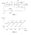
- FIG. 1 is a block diagram representation of a system including a phase locked loop with components that may be used in some embodiments of the invention.
- FIG. 2 is a graphical representation of lines of log f VCO versus log f OUT for different values of division factor N.
- FIG. 3 is a block diagram representation of a dual phase locked loop according to some embodiments of the invention.
- FIG. 4 is a graph of lines of log f CTRL versus log f OUT for different values of division factor N.
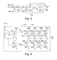
- FIG. 5 is a block diagram representation of a phase frequency detector, charge pump, and loop filter that may be used in some embodiments of the invention.
- FIG. 6 is a block diagram representation of the charge pump of FIG. 5 .
- FIG. 7 is a block diagram representation of the loop filter of FIG. 5 .
- FIG. 8 is a block diagram representation of the voltage controlled oscillator of FIG. 5 .
- FIG. 9 is a block diagram representation of a chip layout for an example of the dual phase locked loop according to some embodiments with scan chain circuitry.
- FIG. 10 is a block chip including a dual phase locked loop according to some embodiments that provides an internal clock signal to circuitry.
- the inventions involves an adaptive-bandwidth PLL with a wide frequency range.
- the frequency range is 500:1, but it could be another ratio.
- the frequency range is extended with a dual-PLL architecture that dynamically adjusts the division factor of a feedforward divider.
- FIG. 1 illustrates a PLL 10 with a phase frequency detector (PFD) 10, a charge pump (CP)/loop filter (LF)16 and output frequency control circuit 20 including a voltage control oscillator (VCO) 22 and a feedforward frequency divider (FF Div) 24 with a division factor of N, and a feedback frequency divider (FB Div) 28 with a division factor of M.
- VCO 22 provides a VCO signal with a frequency f VCO .
- FF Div 24 provides an output clock signal (out clk) with a frequency f OUT that is also provided to FB Div 28.
- the output of FB Div 28 is provided as an input to PFD 14.
- the charge pump and loop filter of CP/LF 16 are different circuits but for convenience of illustration are combined.
- the division factor (N) of FF Div 24 is adjusted. In some embodiments, this adjustment allows FF Div 24 to generate a wide range of frequencies even if the VCO tuning range is relative narrow.
- FIG. 3 illustrates a dual-PLL circuit 50 including two PLLs, sub-PLL 1 and sub-PLL 2, each of which is similar to PLL 10 in FIG. 1 .
- PFD 64 receives the reference clock signal (ref clk) and the output of feedback frequency divider 78, which divides the frequency F OUT1 of out clk1 by M.
- PFD 64 provides a signal(s) to CP/LF 66, which provides a voltage signal V CTRL1 and a voltage signal V FF1 to VCO 72 of output frequency control circuit 70.
- the signal VCO clk 1 is the output of VCO 72 and it is provided to feedforward frequency divider circuit 74, which divides the VCO clk1 signal by N1, where N1 is variable as, for example, is shown in FIGS. 2 and 4 .
- the output clock signal (out clk 1) is the divided VCO clk1 signal and it is provided to selected circuit 78.
- PFD 84 receives the reference clock signal (ref clk) and the output of feedback frequency divider 98, which divides the frequency F OUT2 of out clk1 by M.
- PFD 84 provides a signal(s) to CP/LF 86, which provides a voltage signal V CTRL2 and a voltage signal V FF2 to VCO 82 of output frequency control circuit 90.
- the signal VCO clk 2 is the output of VCO 92 and it is provided to feedfoward frequency divider circuit 94, which divides the VCO clk2 signal by N2, where N2 is variable as, for example, is shown in FIGS. 2 and 4 .
- the output clock signal (out clk 2) is the divided VCO clk2 signal and it is provided to selected circuit 78.
- PLL control circuitry 82 selects the value of N1 and N2 and also provides a selection signal to selection circuit 78 to control whether out clk 1 or out clk 2 is provided by selection circuit 78 as the output signal.
- N1 equals N2 and in other embodiments, N1 and N2 may be different.
- PLL control circuitry 82 receives the V CTRL1 and V CTRL2 and the output clock signals out clk 1 and out clk 2 to help with the decisions. In other embodiments, PLL control circuitry 82 receives the VCO clk1 and VCO clk2 signals.
- the frequency range may be extending through the feedforward divider circuits 74 and 94.
- dividers 74 and 94 scale down the VCO frequency (f VCO ) by N1 or N2, instead of letting VCO 72 and 92 oscillate at the low f OUT .
- PLL control circuitry 82 selects N1 and N2.
- the problem of selection is similar to the coarse frequency control problem encountered in LC oscillators with digitally-selectable load capacitors.
- a prior art scheme involves choosing an N that places the VCO control voltage (V CTRL ) between the high- and low-limits provided externally (V H and V L ).
- this scheme may be unsuitable for ring oscillators because they are more sensitive to PVT variations than LC oscillators.
- the external limits V H and V L may be set with conservative margins to guarantee sufficient overlap between the adjacent frequency sub-ranges.
- the selection of N may be made only once at start-up and may be made prudently, with enough margins to accommodate the worst possible PVT variation over time.
- dual-PLL 50 includes two sub-PLLs 1 and 2 with different feedforward division factors N1 and N2.
- One sub-PLL drives the output (out clk) through selection circuit 78 while the other searches for a better N. If the latter does find a better N, it takes over the role of driving the output and the former starts a new search for N. Since only the locked sub-PLL drives the output, the transients from switching N are hidden from the output and the division factor N can change in real-time.
- the optimality ofN is assessed by how close the settled V CTRL is to V OPT and thus the range of V CTRL in use will be centered at V OPT , without having to set V H and V L . Therefore, the aforementioned margins required in the previous scheme are no longer needed.
- the mid- V CTRL level V OPT can be designed to track the PVT conditions of the VCO to always place it in the optimal V CTRL -range for the lowest jitter.
- FIG. 4 illustrates an algorithm to find N1 and N2.
- the VCO-divider pair can generate a wide range of f OUT with a narrow f VCO range of 2:1, assuming that the division factor N takes the powers of 2, although other embodiments are not limited to these details.
- “Settled" refers to the PLL being settled or locked.
- FIG. 4 three types of co-linear lines.
- a solid thin line indicates V CTRL versus f OUT characteristics of sub-PLL 1 for N values equal to 2 even .
- a dashed thin line indicates V CTRL versus f OUT characteristics of sub-PLL 2 for N values equal to 2 odd .
- a solid thick line indicates V CTRL versus f OUT characteristics of the selected PLL (sub-PLL I or sub-PLL 2)
- the frequency lines may overlap such that of the highest frequency of one line may be more than the lowest frequency of the next line.
- the upper end (large dark circle) of a heavy line is directly above the lowest end (small circle) of the next line.
- the sub-PLL with the settled V CTRL closer to the V OPT drives the output.
- the driving sub-PLL is changed when the two V CTRL 's have equal distances to V OPT , that is, when the two sub-PLLs are equally optimal to generate f OUT .
- the output phase may experience a shift due to the difference in static phase offsets. A hysteresis may be added to prevent this phase shift from turning into a high-frequency jitter via chattering.
- both V CTRL 's are higher or lower than V OPT , one of them is deemed too far from V OPT and the unselected sub-PLL may update N by a factor 4 to bring it closer.
- the bandwidth of PLL 50 may vary proportionally with f VCO /(N x M), where N x M is the total division factor.
- V OPT may not be important but discontinuities in frequency should be avoided. That means in FIG. 4 , there should not be substantial space between the upper end (large dark circle) of a heavy line is directly above the lowest end (small circle) of the next line.
- PLL control circuitry 82 enables dynamic and glitch-free switching of the division factor.
- PLL 50 can achieve low jitter by operating the VCO in its best condition only.
- PLL 50 may maintain a more accurate adaptive-bandwidth dynamic than previous implementations.
- FIG. 5 illustrates embodiments of PFD 64 which provides both an up signal and a down signal to charge pump 112.
- CP/LF 66 of FIG. 3 includes charge pump(CP) 112 and loop filter (LP) 114.
- FIGS. 6 , 7 , and 8 provide details of some embodiments of charge pump 112, loop filter 114, and VCO 72, while other embodiments do not include these details.
- FIG. 6 shows an example of charge pump 112 and its biasing circuit according to some embodiments, while other embodiments do not include these details.
- the charge pump current is biased to track the VCO current, by settling V BN (biased negative) equal to V CTRL1 through V BN being provided as a feedback signal to comparator 122.
- the feedback controls V BP (bias positive) so that the up and down currents are matched within, for example, 2% to reduce static phase offsets.
- Charge pump 112 is segmented to scale the current level by x1, x1/2, and x1/4 for NM of 1, 2, and 4, respectively
- the gates of P-channel metal oxide semiconductor field effect transistors (PMOSFETs) Q11, Q12, Q13, Q14, and Q15 receive the output (V BP signal) of comparator 122, while the gates of N-channel metal oxide semiconductor field effect transistors (NMOSFETs) Q26, Q27, Q28, Q29, and Q30 receive the V BN signal.
- PMOSFETs P-channel metal oxide semiconductor field effect transistors
- NMOSFETs N-channel metal oxide semiconductor field effect transistors
- PMOSFETs Q17, Q18, Q19, and Q20 receive Up signals UP 0 *, UP 1 *, UP 2 *, and UP 2 * where UP 0 *, UP 1 *, and UP 2 *, are the logical inverses of UP 0 , UP 1 , and UP 2 .
- UP 2 has twice the weight as UP 0 and UP 1 .
- NMOSFETs Q22, Q23, Q24, and Q25 receive Down signals DN 0 , DN 1 , DN 2 , and DN 2 .
- DN 2 has twice the weight as DN 0 and DN 1 .
- PMOSFET Q16 and NMOSFET Q21 are joined between Q11 and Q26, with the V BN signal between Q16 and Q21.
- the charge pump voltage V CP is provided between PMOSFETs Q17, Q18, Q19, and Q20 and NMOSFETs Q22, Q23, Q24, and Q25.
- FIG. 7 shows the loop filter 114 according to some embodiments, while other embodiments do not include these details.
- Loop filter 114 includes a charge redistribution network 116 and a half-duty sampled-feedforward loop filter 118.
- Charge redistribution 116 includes switch S1 and S1* (which is the inverse of S1). Switches S1 and S1* alternative being opened and closed.
- Capacitors C11 and C12 (each having a capacitance Cp) are coupled between ground and nodes N11 and N12, respectively.
- Buffer 112 provides the V CTRL signal. When S1* is closed and S 1 is open, the V CTRL voltage is held in C12.
- V CP and V CTRL voltages combine on node N11 and are stored in C11.
- Each charge sharing across the switch S 1 may halve the error charge stored on V CP at node N11.
- the charge redistribution network 116 may replace the role of a programmable current divider.
- the half-duty sampled feedforward loop filter 118 includes a switch S2 and S2* (which is the inverse of S2).
- C13 and C14 (having capacitance Cp and C1, respectively) are coupled between ground and nodes N13 and N14 respectively.
- Loop filter 114 produces a feedforward pulse V FF that is half a reference cycle long and realizes the desired scaling with the reference frequency f REF .
- Switches S1 and S1* and S2 and S2* are opened and closed to control the charge on capacitors C11, C12, C13, and C14. When S1 is closed, the charge is stored on C11 is shared with C12 and when S2 is closed, the charge on C11 is shared with C13.
- Switch S1* resets voltage on C12. Switches S1 and S1* and S2 and S2* may be controlled by logic that received an output from the VCO circuit of FIG. 8 .
- FIG. 8 illustrates an inverter-based ring oscillator including a replica-compensated supply regulator 144 (including PMOSFETs Q62 and Q64 and NMOSFETs Q63 and Q65).
- the replica-feedback improves supply noise rejection by providing a faster feedback path that responds to supply noise.
- the feedforward voltage V FF from loop filter 114 is received by the gates of NMOSFET Q44 and Q47. When V FF is high (has a high voltage), Q44 and Q74 turn ON pulling the drain of Q42 down.
- regulator voltage V REG is high, NMOSFETs Q43 also pulls down on the drain of PMOSFET Q41 and turns ON PMOSFETs Q41 and Q42.
- V RPL replica of NMOSFETs
- the gates of NMOSFETs Q45 and Q48 receive V BN signal. This may be from the same signal as in FIG. 6 or that can be additional circuitry like that in FIG. 6 to generate the V BN for FIG. 8 .
- FIG. 9 illustrates a circuit layout in a sample chip 200.
- PLL1 includes a LF, divider (DIV), PFD, CP, and VCO.
- PLL2 includes the same components.
- Testing circuits 202 tests PLL1 and PLL2.
- Scan chain 204 provides external circuitry with access to portions of the PLLs through.
- the PLL had a wide N-selection range of 2 1 ⁇ 24 , but the example PLL locked to the reference frequency ranging from 2 MHz to 1 GHz.
- the subthreshold leakage in the charge pump may have limited the operation below 2 MHz.
- the dynamic selection of N operated successfully and the VCO oscillation frequency was confined to a narrow range of 1 to 2 GHz.
- the measured jitter versus the reference frequency f REF and M confirmed that the PLL bandwidth scales with f REF . Since the VCO phase noise dominated the output jitter in the measurement setup, the tracking jitter increased as the bandwidth decreased.
- the dual-PLL architecture keeps the VCO away from the jitter-prone, low-frequency oscillation and therefore achieves lower jitter than the fixed-N PLL.
- the discontinuities in the jitter trend indicated the points where N switches, and the worst-case step change in the static phase offset was 3.6% of the reference cycle. Note that other implementations of the inventions may include different details than those mentioned.
- FIG. 10 illustrates a chip 230 with an external clock signal received by dual PLL 234, which provides an internal clock signal to circuitry 238.
- the inventions are not restricted to any particular type of signaling.
- the input and clock signals can be single ended or differential.
- the clocking can be single data rate, double data rate, quad data rate, etc. In double data rate, a rising falling edge of a single clock signal may be used, or two out of phase clocks may be used.
- the signals may be packetized or non-packetized.
- the division M is the same for circuits 78 and 98, but they could be different.
- the term “embodiment” refers to an implementation.
- Reference in the specification to "an embodiment,” “one embodiment,” “some embodiments,” or “other embodiments” means that a particular feature, structure, or characteristic described in connection with the embodiments is included in at least some embodiments, but not necessarily all embodiments, of the inventions. Different references to “some embodiments” do not necessarily refer to the same “some embodiments.”
Landscapes
- Stabilization Of Oscillater, Synchronisation, Frequency Synthesizers (AREA)
Abstract
Description
- Embodiments of the inventions relate generally to phase locked loops.
- Phase locked loops (PLLs) are commonly used in integrated circuit chips and systems to generate a signal that has a frequency and phase related to an input signal, called a reference signal. The reference signal is typically a clock signal. The output signal of the PLL is typically also a clock signal that is "locked" to the input reference clock signal. PLLs are used in a wide variety of chips including microprocessor, communications, and other electronics.
- A typical PLL includes a phase frequency detector (PFD), a charge pump (CP), a loop filter (LF) (which may be a low-pass filter), a voltage controlled oscillator (VCO), and frequency divider circuit. The PFD compares the phase of the reference signal with a feedback signal from the frequency divider circuit. Depending on the relationship of the phase of the reference signal and the feedback signal, the PFD provides a signal(s) to the CP that instructs the CP to increase or decrease the voltage to the VCO through the LF. The LF may integrate the signal to smooth it. The smoothed signal is provided to the VCO. The frequency of the VCO increases or decreases depending on the voltage signal from the LF. The output of the VCO is fed back to the PFD through the frequency divider in a loop that causes the output signal of the VCO to have a frequency that is proportional to (or equal to) and in phase with the reference signal.
- Many PFDs can respond to frequency differences, which increases the lock-in range of allowable inputs. Some PLLs include a divider circuit between a reference clock signal and the reference input to the phase detector. In some designs, there are two outputs of the PFD: one with an up signal that causes the CP to increase the voltage to the VCO and another with a down signal that causes the CP to decrease the voltage to the VCO.
- Adaptive-bandwidth PLL refers to a class of PLL that scales its dynamics proportionally with the operating frequency largely regardless of the process, voltage, and temperature (PVT) variations.
- One of the challenges that analog PLL designers face today is the reduction in the ring VCO frequency range. The usable range of the VCO control voltage has shrunk considerably as the supply voltage has scaled below 1.2V (volts). On the other hand, the PLL application space continues to expand, demanding even wider frequency range from a single PLL.
- Accordingly, in a first aspect, the present invention provides a chip according to
Claim 1, Other aspects and embodiments are set out below. - In some embodiments, a chip includes first and second sub phase lock loops (sub-PLLs) including first and second voltage controlled oscillators (VCOs) to provide first and second VCO output signals and first and second feedforward divider circuits to divide first and second frequencies of the first and second VCO output signals by first and second division factors. The chip also includes phase locked loop control circuitry to select the first and second division factors.
- In some embodiments, the PLL control circuitry selects the first and second division factors in response to the first and second output clock signals and the first and second feedfoward voltage signal inputs into the first and second VCOs.
- In some embodiments, a method includes providing first and second voltage controlled oscillators (VCOs) of first and second sub phase lock loops (sub-PLLs) with voltage control signals. The method further includes outputting first and second VCO output signals and first and second feedforward divider circuits from the first and second VCOs, dividing first and second frequencies of the first and second VCO output signals by first and second division factors, and selecting the first and second division factors.
- In further embodiments, a chip includes at least one conductor carrying an input clock signal and a dual phase locked loop (dual-PLL). The dual-PLL includes first and second sub phase lock loops (sub-PLLs) including first and second voltage controlled oscillators (VCOs) to provide first and second VCO output signals and first and second feedforward divider circuits to divide first and second frequencies of the first and second VCO output signals by first and second division factors; and phase locked loop control circuitry to select the first and second division factors.
- Other embodiments are described and claimed.
- The inventions may be understood by referring to the following description and accompanying drawings that are used to illustrate embodiments of the invention. However, the inventions are not limited to the details of these drawings.
-
FIG. 1 is a block diagram representation of a system including a phase locked loop with components that may be used in some embodiments of the invention. -
FIG. 2 is a graphical representation of lines of log fVCO versus log fOUT for different values of division factor N. -
FIG. 3 is a block diagram representation of a dual phase locked loop according to some embodiments of the invention. -
FIG. 4 is a graph of lines of log fCTRL versus log fOUT for different values of division factor N. -
FIG. 5 is a block diagram representation of a phase frequency detector, charge pump, and loop filter that may be used in some embodiments of the invention. -
FIG. 6 is a block diagram representation of the charge pump ofFIG. 5 . -
FIG. 7 is a block diagram representation of the loop filter ofFIG. 5 . -
FIG. 8 is a block diagram representation of the voltage controlled oscillator ofFIG. 5 . -
FIG. 9 is a block diagram representation of a chip layout for an example of the dual phase locked loop according to some embodiments with scan chain circuitry. -
FIG. 10 is a block chip including a dual phase locked loop according to some embodiments that provides an internal clock signal to circuitry. - In some embodiments, the inventions involves an adaptive-bandwidth PLL with a wide frequency range. Merely as an example, in some implementations, the frequency range is 500:1, but it could be another ratio. In some embodiments, the frequency range is extended with a dual-PLL architecture that dynamically adjusts the division factor of a feedforward divider.
-
FIG. 1 illustrates aPLL 10 with a phase frequency detector (PFD) 10, a charge pump (CP)/loop filter (LF)16 and outputfrequency control circuit 20 including a voltage control oscillator (VCO) 22 and a feedforward frequency divider (FF Div) 24 with a division factor of N, and a feedback frequency divider (FB Div) 28 with a division factor ofM. VCO 22 provides a VCO signal with a frequency fVCO. FF Div 24 provides an output clock signal (out clk) with a frequency fOUT that is also provided to FB Div 28. The output of FB Div 28 is provided as an input toPFD 14. The charge pump and loop filter of CP/LF 16 are different circuits but for convenience of illustration are combined. The division factor (N) of FF Div 24 is adjusted. In some embodiments, this adjustment allows FF Div 24 to generate a wide range of frequencies even if the VCO tuning range is relative narrow. -
FIG. 2 illustrates a graph of lines of log fVCO versus log fOUT for different values of division factor N, for example, N = 24, N = 23 , N = 22 , N = 21. As the frequency of fVCO increases between fO and fO/2, the frequency of fOUT increases beginning at fO/24 for N = 24, beginning at fo /23 for N = 23, beginning at fO/22 for N = 22, and beginning at fO/21 for N = 21. Note that the frequency lines may overlap such that of the highest frequency of one line (for example, the N = 24 line) may be more than the lowest frequency of the next line (for example, the N =23 line). -
FIG. 3 illustrates a dual-PLL circuit 50 including two PLLs,sub-PLL 1 andsub-PLL 2, each of which is similar toPLL 10 inFIG. 1 . Insub-PLL 1,PFD 64 receives the reference clock signal (ref clk) and the output offeedback frequency divider 78, which divides the frequency FOUT1 of out clk1 byM. PFD 64 provides a signal(s) to CP/LF 66, which provides a voltage signal VCTRL1 and a voltage signal VFF1 toVCO 72 of outputfrequency control circuit 70. Thesignal VCO clk 1 is the output ofVCO 72 and it is provided to feedforwardfrequency divider circuit 74, which divides the VCO clk1 signal by N1, where N1 is variable as, for example, is shown inFIGS. 2 and4 . The output clock signal (out clk 1) is the divided VCO clk1 signal and it is provided to selectedcircuit 78. - In
sub-PLL 2,PFD 84 receives the reference clock signal (ref clk) and the output offeedback frequency divider 98, which divides the frequency FOUT2 of out clk1 byM. PFD 84 provides a signal(s) to CP/LF 86, which provides a voltage signal VCTRL2 and a voltage signal VFF2 toVCO 82 of outputfrequency control circuit 90. Thesignal VCO clk 2 is the output ofVCO 92 and it is provided to feedfowardfrequency divider circuit 94, which divides the VCO clk2 signal by N2, where N2 is variable as, for example, is shown inFIGS. 2 and4 . The output clock signal (out clk 2) is the divided VCO clk2 signal and it is provided to selectedcircuit 78. -
PLL control circuitry 82 selects the value of N1 and N2 and also provides a selection signal toselection circuit 78 to control whether outclk 1 or outclk 2 is provided byselection circuit 78 as the output signal. In some embodiments, N1 equals N2 and in other embodiments, N1 and N2 may be different. In some embodiments,PLL control circuitry 82 receives the VCTRL1 and VCTRL2 and the output clock signals outclk 1 and outclk 2 to help with the decisions. In other embodiments,PLL control circuitry 82 receives the VCO clk1 and VCO clk2 signals. - In
FIG. 3 , the frequency range may be extending through thefeedforward divider circuits dividers VCO PLL control circuitry 82 selects N1 and N2. In some embodiments, the problem of selection is similar to the coarse frequency control problem encountered in LC oscillators with digitally-selectable load capacitors. A prior art scheme involves choosing an N that places the VCO control voltage (VCTRL) between the high- and low-limits provided externally (VH and VL). However, this scheme may be unsuitable for ring oscillators because they are more sensitive to PVT variations than LC oscillators. First, to ensure seamless coverage of frequency, the external limits VH and VL may be set with conservative margins to guarantee sufficient overlap between the adjacent frequency sub-ranges. Second, since changing N may cause the PLL to lose lock momentarily, the selection of N may be made only once at start-up and may be made prudently, with enough margins to accommodate the worst possible PVT variation over time. These margins call for a wide tuning range of the VCO, diminishing the benefits of thefeedforward divider circuits - The proposed dual-PLL circuitry (such as in
FIG. 3 ) may eliminate the need for those margins by allowing N to change dynamically and using a single voltage VOPT to set the mid level of VCTRL. As depicted inFIG. 3 , dual-PLL 50 includes twosub-PLLs selection circuit 78 while the other searches for a better N. If the latter does find a better N, it takes over the role of driving the output and the former starts a new search for N. Since only the locked sub-PLL drives the output, the transients from switching N are hidden from the output and the division factor N can change in real-time. The optimality ofN is assessed by how close the settled VCTRL is to VOPT and thus the range of VCTRL in use will be centered at VOPT, without having to set VH and VL. Therefore, the aforementioned margins required in the previous scheme are no longer needed. In addition, the mid- VCTRL level VOPT can be designed to track the PVT conditions of the VCO to always place it in the optimal VCTRL -range for the lowest jitter. -
FIG. 4 illustrates an algorithm to find N1 and N2. Merely as an example, in some embodiments, the VCO-divider pair can generate a wide range of fOUT with a narrow fVCO range of 2:1, assuming that the division factor N takes the powers of 2, although other embodiments are not limited to these details.FIG. 4 illustrates a graph of lines of settled fCTRL versus log fOUT for different values of division factor N, for example, N = 26, N = 25, N = 24, N = 23, N = 22, N = 21. "Settled" refers to the PLL being settled or locked.FIG. 4 three types of co-linear lines. A solid thin line indicates VCTRL versus fOUT characteristics of sub-PLL 1 for N values equal to 2even. A dashed thin line indicates VCTRL versus fOUT characteristics of sub-PLL 2 for N values equal to 2odd. A solid thick line indicates VCTRL versus fOUT characteristics of the selected PLL (sub-PLL I or sub-PLL 2) Like inFIG. 2 , the frequency lines may overlap such that of the highest frequency of one line may be more than the lowest frequency of the next line. However, the upper end (large dark circle) of a heavy line is directly above the lowest end (small circle) of the next line. For example, the small circle at the bottom of line N=24 has the same fOUT value as the top (large circle) of the heavy line of N=25. - The sub-PLL with the settled VCTRL closer to the VOPT drives the output. The driving sub-PLL is changed when the two VCTRL's have equal distances to VOPT, that is, when the two sub-PLLs are equally optimal to generate fOUT. Upon the switch, the output phase may experience a shift due to the difference in static phase offsets. A hysteresis may be added to prevent this phase shift from turning into a high-frequency jitter via chattering. Also, when both VCTRL's are higher or lower than VOPT, one of them is deemed too far from VOPT and the unselected sub-PLL may update N by a factor 4 to bring it closer. The bandwidth of
PLL 50 may vary proportionally with fVCO/(N x M), where N x M is the total division factor. There are different ways to choose the value of VOPT. The precise value of VOPT may not be important but discontinuities in frequency should be avoided. That means inFIG. 4 , there should not be substantial space between the upper end (large dark circle) of a heavy line is directly above the lowest end (small circle) of the next line. - In some embodiments,
PLL control circuitry 82 enables dynamic and glitch-free switching of the division factor. In some embodiments, by leveraging a relatively narrow tuning range,PLL 50 can achieve low jitter by operating the VCO in its best condition only. Also, with the loop bandwidth explicitly controlled by the division factor N,PLL 50 may maintain a more accurate adaptive-bandwidth dynamic than previous implementations. -
FIG. 5 illustrates embodiments ofPFD 64 which provides both an up signal and a down signal to chargepump 112. InFIG. 5 , CP/LF 66 ofFIG. 3 includes charge pump(CP) 112 and loop filter (LP) 114.FIGS. 6 ,7 , and8 provide details of some embodiments ofcharge pump 112,loop filter 114, andVCO 72, while other embodiments do not include these details. -
FIG. 6 shows an example ofcharge pump 112 and its biasing circuit according to some embodiments, while other embodiments do not include these details. For adaptive bandwidth, the charge pump current is biased to track the VCO current, by settling VBN (biased negative) equal to VCTRL1 through VBN being provided as a feedback signal tocomparator 122. Also, the feedback controls VBP (bias positive) so that the up and down currents are matched within, for example, 2% to reduce static phase offsets.Charge pump 112 is segmented to scale the current level by x1, x1/2, and x1/4 for NM of 1, 2, and 4, respectively The gates of P-channel metal oxide semiconductor field effect transistors (PMOSFETs) Q11, Q12, Q13, Q14, and Q15 receive the output (VBP signal) ofcomparator 122, while the gates of N-channel metal oxide semiconductor field effect transistors (NMOSFETs) Q26, Q27, Q28, Q29, and Q30 receive the VBN signal. PMOSFETs Q17, Q18, Q19, and Q20 receive Up signals UP0*, UP1*, UP2*, and UP2* where UP0*, UP1*, and UP2*, are the logical inverses of UP0, UP1, and UP2. Note that UP2 has twice the weight as UP0 and UP1. NMOSFETs Q22, Q23, Q24, and Q25 receive Down signals DN0, DN1, DN2, and DN2. Note that DN2 has twice the weight as DN0 and DN1. PMOSFET Q16 and NMOSFET Q21 are joined between Q11 and Q26, with the VBN signal between Q16 and Q21. The charge pump voltage VCP is provided between PMOSFETs Q17, Q18, Q19, and Q20 and NMOSFETs Q22, Q23, Q24, and Q25. -
FIG. 7 shows theloop filter 114 according to some embodiments, while other embodiments do not include these details.Loop filter 114 includes acharge redistribution network 116 and a half-duty sampled-feedforward loop filter 118.Charge redistribution 116 includes switch S1 and S1* (which is the inverse of S1). Switches S1 and S1* alternative being opened and closed. Capacitors C11 and C12 (each having a capacitance Cp) are coupled between ground and nodes N11 and N12, respectively.Buffer 112 provides the VCTRL signal. When S1* is closed andS 1 is open, the VCTRL voltage is held in C12. WhenS 1 is closed and S1* is open, the VCP and VCTRL voltages combine on node N11 and are stored in C11. Each charge sharing across theswitch S 1 may halve the error charge stored on VCP at node N11. Thecharge redistribution network 116 may replace the role of a programmable current divider. The programmable divider generates the control signals to sequence the switches and scale down the loop gain by N x M/4 (=2n+m-2) for N x M greater than 4. - The half-duty sampled
feedforward loop filter 118 includes a switch S2 and S2* (which is the inverse of S2). C13 and C14 (having capacitance Cp and C1, respectively) are coupled between ground and nodes N13 and N14 respectively.Loop filter 114 produces a feedforward pulse VFF that is half a reference cycle long and realizes the desired scaling with the reference frequency fREF. Switches S1 and S1* and S2 and S2* are opened and closed to control the charge on capacitors C11, C12, C13, and C14. When S1 is closed, the charge is stored on C11 is shared with C12 and when S2 is closed, the charge on C11 is shared with C13. Switch S1* resets voltage on C12. Switches S1 and S1* and S2 and S2* may be controlled by logic that received an output from the VCO circuit ofFIG. 8 . -
FIG. 8 illustrates an inverter-based ring oscillator including a replica-compensated supply regulator 144 (including PMOSFETs Q62 and Q64 and NMOSFETs Q63 and Q65). The replica-feedback improves supply noise rejection by providing a faster feedback path that responds to supply noise. The feedforward voltage VFF fromloop filter 114 is received by the gates of NMOSFET Q44 and Q47. When VFF is high (has a high voltage), Q44 and Q74 turn ON pulling the drain of Q42 down. When regulator voltage VREG is high, NMOSFETs Q43 also pulls down on the drain of PMOSFET Q41 and turns ON PMOSFETs Q41 and Q42. When Q44, Q47, Q42 are ON, node N15 is pulled low turning ON PMOSFET Q61. A voltage VRPL (replica) at the drain of Q61 turns ON NMOSFET Q46. The gates of NMOSFETs Q45 and Q48 receive VBN signal. This may be from the same signal as inFIG. 6 or that can be additional circuitry like that inFIG. 6 to generate the VBN forFIG. 8 . - When the voltage of N15 is pulled down, PMOSFET Q71 turns ON, which pulls up VREG up and turns OFF Q43. Capacitor C20 smoothes out voltage changes. Voltage VREG controls the rate at which inverters I1, I2, I3, I4, and I5 oscillate and, therefore, control the frequency of the VCO1 clock signal provided from inverter I5.
-
FIG. 9 illustrates a circuit layout in asample chip 200. PLL1 includes a LF, divider (DIV), PFD, CP, and VCO. PLL2 includes the same components.Testing circuits 202 tests PLL1 and PLL2.Scan chain 204 provides external circuitry with access to portions of the PLLs through. An adaptive-bandwidth PLL was implemented in a 0.13µm CMOS process and had the following characteristics:Process Technology: 0.13 µm N-well 1P6M CMOS Area: 1.1 x 0.46mm2 Supply voltage: 1.2V nominal Power dissipation: 36mW Reference frequency range: 2MHz ~ 1 GHz Output frequency range: 2MHz ~ 1 GHz Multiplication factor range: M = 20~9 Loop bandwidth: ~1/100 of reference frequency Jitter (M=1, 1.024GHz) 13.10ps, pp, 1.62ps, rms - In the example, the PLL had a wide N-selection range of 21 ~ 24, but the example PLL locked to the reference frequency ranging from 2 MHz to 1 GHz. The subthreshold leakage in the charge pump may have limited the operation below 2 MHz. The dynamic selection of N operated successfully and the VCO oscillation frequency was confined to a narrow range of 1 to 2 GHz. The PLL could provide any multiplied frequency with M=2m as long as M x fREF is no greater that 1 GHz. The measured jitter versus the reference frequency fREF and M confirmed that the PLL bandwidth scales with fREF. Since the VCO phase noise dominated the output jitter in the measurement setup, the tracking jitter increased as the bandwidth decreased. By self-adapting N to fOUT, the dual-PLL architecture keeps the VCO away from the jitter-prone, low-frequency oscillation and therefore achieves lower jitter than the fixed-N PLL. The discontinuities in the jitter trend indicated the points where N switches, and the worst-case step change in the static phase offset was 3.6% of the reference cycle. Note that other implementations of the inventions may include different details than those mentioned.
-
FIG. 10 illustrates achip 230 with an external clock signal received bydual PLL 234, which provides an internal clock signal tocircuitry 238. - The inventions are not restricted to any particular type of signaling. The input and clock signals can be single ended or differential. The clocking can be single data rate, double data rate, quad data rate, etc. In double data rate, a rising falling edge of a single clock signal may be used, or two out of phase clocks may be used. The signals may be packetized or non-packetized.
- This disclosures includes various figures that are schematic in nature and do not include various details. In actual implementations, the systems and chips would include additional components that are not illustrated including between circuitry illustrated in the figures. The illustrated components may have various additional inputs and outputs. Various algorithms and methods described herein may be performed in hardware circuitry without or without the assistance of firmware or software. However, firmware and/or software may be used in overall systems in which the algorithms and methods are performed.
- In
FIG. 3 , the division M is the same forcircuits - As used herein, the term "embodiment" refers to an implementation. Reference in the specification to "an embodiment," "one embodiment," "some embodiments," or "other embodiments" means that a particular feature, structure, or characteristic described in connection with the embodiments is included in at least some embodiments, but not necessarily all embodiments, of the inventions. Different references to "some embodiments" do not necessarily refer to the same "some embodiments."
- If the specification states a component, feature, structure, or characteristic "may", "might", or "could" be included, that particular component, feature, structure, or characteristic is not required to be included. If the specification or claim refers to "a" structure, that does not mean there is only one of the structure.
- While the invention has been described in terms of several embodiments, the invention should not limited to only those embodiments described, but can be practiced with modification and alteration within the spirit and scope of the appended claims. The description is thus to be regarded as illustrative instead of limiting.
Claims (20)
- A chip comprising:first and second sub phase lock loops (sub-PLLs) including first and second voltage controlled oscillators (VCOs) to provide first and second VCO output signals and first and second feedforward divider circuits to divide first and second frequencies of the first and second VCO output signals by first and second division factors; andphase locked loop control circuitry to select the first and second division factors.
- The chip of claim 1, wherein the PLL control circuitry selects the first and second division factors in response to the first and second output clock signals and the first and second feedfoward voltage signal inputs into the first and second VCOs.
- The chip of claim 1, wherein the first division factor is typically different than the second division factor.
- The chip of claim 1, wherein the PLL control circuitry selects the first and second division factors while considering an optimal voltage value.
- The chip of claim 1, further comprising output signal selection circuitry to select either the divided first and second VCO output signals under the control of the phase locked loop control circuitry.
- The chip of claim 1, wherein the first division factor is equal to 2 raised to an integer power and the second first division factor is equal to 2 raised to an integer power, and wherein the integer for the first division factor is typically different than the integer for the second division factor.
- The chip of claim 6, wherein the integers of the first sub-PLL are even integers and the integers of the second sub-PLL are odd integers.
- The chip of claim 1, wherein while one sub-PLL is provide the output, PLL control circuitry may change the division factor for the other sub-PLL.
- The chip of claim 1, wherein the first and second sub-PLLs include:first and second phase frequency detectors; andfirst and second feedback divider circuits to divide the frequency of divided first and second VCO output signals and provide them to the first and second phase frequency detectors.
- A method comprising:providing first and second voltage controlled oscillators (VCOs) of first and second sub phase lock loops (sub-PLLs) with voltage control signals;outputting first and second VCO output signals and first and second feedforward divider circuits from the first and second VCOs;dividing first and second frequencies of the first and second VCO output signals by first and second division factors; andselecting the first and second division factors.
- The method of claim 10, further comprising selecting the output of the first or the second sub-PLLs as a PLL output signal.
- The method of claim 10, wherein the PLL control circuitry selects the first and second division factors in response to the first and second output clock signals and the first and second feedfoward voltage signal inputs into the first and second VCOs.
- The method of claim 10, wherein the first division factor is typically different than the second division factor.
- The method of claim 10, wherein PLL control circuitry selects the first and second division factors while considering an optimal voltage value.
- A chip comprising:at least one conductor carrying an input clock signal;a dual phase locked loop (dual-PLL) including:first and second sub phase lock loops (sub-PLLs) including first and second voltage controlled oscillators (VCOs) to provide first and second VCO output signals and first and second feedforward divider circuits to divide first and second frequencies of the first and second VCO output signals by first and second division factors; andphase locked loop control circuitry to select the first and second division factors.
- The chip of claim 15, wherein the PLL control circuitry selects the first and second division factors in response to the first and second output clock signals and the first and second feedfoward voltage signal inputs into the first and second VCOs.
- The chip of claim 15, wherein the first division factor is typically different than the second division factor.
- The chip of claim 15, wherein the PLL control circuitry selects the first and second division factors while considering an optimal voltage value.
- The chip of claim 15, further comprising output signal selection circuitry to select either the divided first and second VCO output signals under the control of the phase locked loop control circuitry.
- The chip of claim 15, wherein the first division factor is equal to 2 raised to an integer power and the second first division factor is equal to 2 raised to an integer power, and wherein the integer for the first division factor is typically different than the integer for the second division factor.
Applications Claiming Priority (1)
| Application Number | Priority Date | Filing Date | Title |
|---|---|---|---|
| US11/637,254 US7602253B2 (en) | 2006-12-11 | 2006-12-11 | Adaptive bandwidth phase locked loop with feedforward divider |
Publications (2)
| Publication Number | Publication Date |
|---|---|
| EP1933464A1 true EP1933464A1 (en) | 2008-06-18 |
| EP1933464B1 EP1933464B1 (en) | 2010-09-15 |
Family
ID=38996611
Family Applications (1)
| Application Number | Title | Priority Date | Filing Date |
|---|---|---|---|
| EP07254315A Active EP1933464B1 (en) | 2006-12-11 | 2007-10-31 | Adaptive bandwith phase locked loop with feedforward divider |
Country Status (7)
| Country | Link |
|---|---|
| US (1) | US7602253B2 (en) |
| EP (1) | EP1933464B1 (en) |
| JP (1) | JP5515216B2 (en) |
| KR (1) | KR101470990B1 (en) |
| CN (1) | CN101202546B (en) |
| DE (1) | DE602007009176D1 (en) |
| TW (1) | TWI356592B (en) |
Families Citing this family (15)
| Publication number | Priority date | Publication date | Assignee | Title |
|---|---|---|---|---|
| US7747237B2 (en) * | 2004-04-09 | 2010-06-29 | Skyworks Solutions, Inc. | High agility frequency synthesizer phase-locked loop |
| US20080317185A1 (en) * | 2007-06-25 | 2008-12-25 | Broadcom Corporation | Dual phase locked loop (pll) architecture for multi-mode operation in communication systems |
| US7821343B1 (en) * | 2008-08-27 | 2010-10-26 | Altera Corporation | Transmitter with multiple phase locked loops |
| TWI384761B (en) * | 2009-02-20 | 2013-02-01 | Sunplus Technology Co Ltd | Low jitter, wide operating frequency band and frequency synthesis system suitable for low voltage operation |
| US8044726B2 (en) * | 2009-03-17 | 2011-10-25 | Qualcomm Incorporated | Systems and methods for self testing a voltage controlled oscillator |
| US7973612B2 (en) * | 2009-04-26 | 2011-07-05 | Qualcomm Incorporated | Supply-regulated phase-locked loop (PLL) and method of using |
| JP2011188077A (en) * | 2010-03-05 | 2011-09-22 | Renesas Electronics Corp | Phase locked loop circuit and control method thereof |
| US8415999B2 (en) | 2010-07-28 | 2013-04-09 | International Business Machines Corporation | High frequency quadrature PLL circuit and method |
| US8258835B1 (en) * | 2011-06-15 | 2012-09-04 | Asahi Kasei Microdevices Corporation | Cancellation system for phase jumps at loop gain changes in fractional-N frequency synthesizers |
| CN103269220A (en) * | 2013-05-30 | 2013-08-28 | 上海坤锐电子科技有限公司 | Clock recovery circuit through NFC active load modulation based on digital phase-locked loop |
| CN103346784B (en) * | 2013-06-18 | 2016-04-13 | 成都嘉纳海威科技有限责任公司 | A kind of matching type charge pump circuit for phase-locked loop |
| US9350362B2 (en) | 2013-10-08 | 2016-05-24 | Thomas & Betts International, Llc | Programmable slew rate phase locked loop |
| US9444473B2 (en) * | 2014-09-09 | 2016-09-13 | Qualcomm Incorporated | Increased synthesizer performance in carrier aggregation/multiple-input, multiple-output systems |
| ES2719545T3 (en) | 2015-04-15 | 2019-07-11 | Mitsubishi Electric Corp | Synthesizer |
| US10958278B2 (en) | 2019-07-31 | 2021-03-23 | Intel Corporation | Techniques in phase-lock loop configuration in a computing device |
Citations (3)
| Publication number | Priority date | Publication date | Assignee | Title |
|---|---|---|---|---|
| JPS60197015A (en) * | 1984-03-21 | 1985-10-05 | Nec Corp | Phase locked oscillator |
| GB2295930A (en) * | 1994-12-06 | 1996-06-12 | Motorola Ltd | Frequency hopping in a TDMA system |
| US5610558A (en) * | 1995-11-03 | 1997-03-11 | Motorola, Inc. | Controlled tracking of oscillators in a circuit with multiple frequency sensitive elements |
Family Cites Families (24)
| Publication number | Priority date | Publication date | Assignee | Title |
|---|---|---|---|---|
| JPS63305619A (en) * | 1987-06-08 | 1988-12-13 | Mitsubishi Electric Corp | Pll synthesizer device |
| JPH01120133U (en) * | 1988-02-06 | 1989-08-15 | ||
| JPH03190428A (en) * | 1989-12-20 | 1991-08-20 | Matsushita Electric Ind Co Ltd | Phase synchronizing circuit |
| JPH05145413A (en) * | 1991-11-20 | 1993-06-11 | Nippon Denki Musen Denshi Kk | Phase locked loop circuit |
| JPH05199109A (en) * | 1992-01-20 | 1993-08-06 | Ricoh Co Ltd | Pll circuit |
| JPH05227024A (en) * | 1992-02-12 | 1993-09-03 | Sony Tektronix Corp | Pll oscillation device |
| US5483202A (en) * | 1994-08-31 | 1996-01-09 | Polaroid Corporation | Compensated phase locked loop for generating a controlled output clock signal |
| JPH08125529A (en) * | 1994-10-20 | 1996-05-17 | Fujitsu General Ltd | Pll circuit |
| JPH10271002A (en) * | 1997-03-21 | 1998-10-09 | Sony Corp | Oscillation controller |
| US6049254A (en) * | 1997-10-16 | 2000-04-11 | Oasis Design, Inc. | Phase-locked loop which can automatically adjust to and lock upon a variable input frequency |
| JPH11136124A (en) * | 1997-10-27 | 1999-05-21 | Matsushita Electric Ind Co Ltd | Pll circuit |
| JPH11214992A (en) * | 1998-01-23 | 1999-08-06 | Mitsubishi Electric Corp | Frequency synthesizer |
| US6111442A (en) * | 1998-03-09 | 2000-08-29 | International Business Machines Corporation | Phase-locked loop circuit with dynamic backup |
| JP2000252821A (en) * | 1999-02-26 | 2000-09-14 | Ando Electric Co Ltd | Clock generating circuit for communication unit and method for generating clock of the communication unit |
| KR20010059868A (en) | 1999-12-30 | 2001-07-06 | 윤종용 | Method for generating frequency in dual phase locked loop |
| GB2363268B (en) | 2000-06-08 | 2004-04-14 | Mitel Corp | Timing circuit with dual phase locked loops |
| JP2002064378A (en) * | 2000-08-18 | 2002-02-28 | Advantest Corp | Signal generator |
| US6281727B1 (en) | 2000-10-05 | 2001-08-28 | Pericom Semiconductor Corp. | Fine-tuning phase-locked loop PLL using variable resistor between dual PLL loops |
| US6670833B2 (en) | 2002-01-23 | 2003-12-30 | Intel Corporation | Multiple VCO phase lock loop architecture |
| US7290156B2 (en) | 2003-12-17 | 2007-10-30 | Via Technologies, Inc. | Frequency-voltage mechanism for microprocessor power management |
| US7302599B2 (en) | 2004-02-12 | 2007-11-27 | Via Technologies, Inc. | Instantaneous frequency-based microprocessor power management |
| US6812797B1 (en) | 2003-05-30 | 2004-11-02 | Agere Systems Inc. | Phase-locked loop with loop select signal based switching between frequency detection and phase detection |
| US6762634B1 (en) | 2003-08-13 | 2004-07-13 | Pericom Semiconductor Corp. | Dual-loop PLL with DAC offset for frequency shift while maintaining input tracking |
| US7630468B2 (en) | 2003-12-19 | 2009-12-08 | Broadcom Corporation | Dual-PLL signaling for maintaining synchronization in a communications system |
-
2006
- 2006-12-11 US US11/637,254 patent/US7602253B2/en active Active
-
2007
- 2007-10-24 TW TW096139964A patent/TWI356592B/en active
- 2007-10-31 EP EP07254315A patent/EP1933464B1/en active Active
- 2007-10-31 DE DE602007009176T patent/DE602007009176D1/en active Active
- 2007-12-10 KR KR1020070127886A patent/KR101470990B1/en active IP Right Grant
- 2007-12-10 CN CN2007101942310A patent/CN101202546B/en active Active
- 2007-12-11 JP JP2007341739A patent/JP5515216B2/en active Active
Patent Citations (3)
| Publication number | Priority date | Publication date | Assignee | Title |
|---|---|---|---|---|
| JPS60197015A (en) * | 1984-03-21 | 1985-10-05 | Nec Corp | Phase locked oscillator |
| GB2295930A (en) * | 1994-12-06 | 1996-06-12 | Motorola Ltd | Frequency hopping in a TDMA system |
| US5610558A (en) * | 1995-11-03 | 1997-03-11 | Motorola, Inc. | Controlled tracking of oscillators in a circuit with multiple frequency sensitive elements |
Also Published As
| Publication number | Publication date |
|---|---|
| CN101202546B (en) | 2012-12-26 |
| TWI356592B (en) | 2012-01-11 |
| TW200830719A (en) | 2008-07-16 |
| JP2008148346A (en) | 2008-06-26 |
| EP1933464B1 (en) | 2010-09-15 |
| CN101202546A (en) | 2008-06-18 |
| US20080136531A1 (en) | 2008-06-12 |
| US7602253B2 (en) | 2009-10-13 |
| JP5515216B2 (en) | 2014-06-11 |
| KR101470990B1 (en) | 2014-12-12 |
| DE602007009176D1 (en) | 2010-10-28 |
| KR20080053902A (en) | 2008-06-16 |
Similar Documents
| Publication | Publication Date | Title |
|---|---|---|
| EP1933464B1 (en) | Adaptive bandwith phase locked loop with feedforward divider | |
| US8508308B2 (en) | Automatic frequency calibration of a multi-LCVCO phase locked loop with adaptive thresholds and programmable center control voltage | |
| US5757240A (en) | Low gain voltage-controlled oscillator | |
| US6057739A (en) | Phase-locked loop with variable parameters | |
| US7696799B2 (en) | Delay cell of voltage controlled delay line using digital and analog control scheme | |
| US7161398B2 (en) | VCDL-based dual loop DLL having infinite phase shift function | |
| US7339438B2 (en) | Phase and delay locked loops and semiconductor memory device having the same | |
| US6664829B1 (en) | Charge pump using dynamic charge balance compensation circuit and method of operation | |
| KR100319607B1 (en) | Analog dll circuit | |
| US5952892A (en) | Low-gain, low-jitter voltage controlled oscillator circuit | |
| US7379521B2 (en) | Delay circuit with timing adjustment function | |
| US7719331B2 (en) | PLL circuit | |
| US8232822B2 (en) | Charge pump and phase-detecting apparatus, phase-locked loop and delay-locked loop using the same | |
| US7375557B2 (en) | Phase-locked loop and method thereof and a phase-frequency detector and method thereof | |
| US8570113B2 (en) | Digital VCO calibration method and apparatus | |
| US8264259B2 (en) | Phase-locked loop circuit and delay-locked loop circuit | |
| US7764092B2 (en) | Phase locked loop and phase locking method | |
| KR101394762B1 (en) | Phase shifting in dll/pll | |
| US7498886B2 (en) | Clock distribution system and method thereof | |
| US9432028B2 (en) | Clock data recovery circuit and a method of operating the same | |
| US9214946B2 (en) | Phase locked loop circuit | |
| US20140347110A1 (en) | Capacitive load pll with calibration loop | |
| US8373465B1 (en) | Electronic device and method for phase locked loop | |
| KR20130116112A (en) | A phase locked loop, frequency control circuit of pll, and locking method of pll |
Legal Events
| Date | Code | Title | Description |
|---|---|---|---|
| PUAI | Public reference made under article 153(3) epc to a published international application that has entered the european phase |
Free format text: ORIGINAL CODE: 0009012 |
|
| AK | Designated contracting states |
Kind code of ref document: A1 Designated state(s): AT BE BG CH CY CZ DE DK EE ES FI FR GB GR HU IE IS IT LI LT LU LV MC MT NL PL PT RO SE SI SK TR |
|
| AX | Request for extension of the european patent |
Extension state: AL BA HR MK RS |
|
| 17P | Request for examination filed |
Effective date: 20081113 |
|
| 17Q | First examination report despatched |
Effective date: 20081215 |
|
| AKX | Designation fees paid |
Designated state(s): DE FR GB TR |
|
| GRAP | Despatch of communication of intention to grant a patent |
Free format text: ORIGINAL CODE: EPIDOSNIGR1 |
|
| GRAS | Grant fee paid |
Free format text: ORIGINAL CODE: EPIDOSNIGR3 |
|
| GRAA | (expected) grant |
Free format text: ORIGINAL CODE: 0009210 |
|
| AK | Designated contracting states |
Kind code of ref document: B1 Designated state(s): DE FR GB TR |
|
| REG | Reference to a national code |
Ref country code: GB Ref legal event code: FG4D |
|
| REF | Corresponds to: |
Ref document number: 602007009176 Country of ref document: DE Date of ref document: 20101028 Kind code of ref document: P |
|
| PLBE | No opposition filed within time limit |
Free format text: ORIGINAL CODE: 0009261 |
|
| STAA | Information on the status of an ep patent application or granted ep patent |
Free format text: STATUS: NO OPPOSITION FILED WITHIN TIME LIMIT |
|
| 26N | No opposition filed |
Effective date: 20110616 |
|
| REG | Reference to a national code |
Ref country code: DE Ref legal event code: R097 Ref document number: 602007009176 Country of ref document: DE Effective date: 20110616 |
|
| PG25 | Lapsed in a contracting state [announced via postgrant information from national office to epo] |
Ref country code: TR Free format text: LAPSE BECAUSE OF FAILURE TO SUBMIT A TRANSLATION OF THE DESCRIPTION OR TO PAY THE FEE WITHIN THE PRESCRIBED TIME-LIMIT Effective date: 20100915 |
|
| REG | Reference to a national code |
Ref country code: FR Ref legal event code: PLFP Year of fee payment: 9 |
|
| REG | Reference to a national code |
Ref country code: FR Ref legal event code: PLFP Year of fee payment: 10 |
|
| REG | Reference to a national code |
Ref country code: FR Ref legal event code: PLFP Year of fee payment: 11 |
|
| REG | Reference to a national code |
Ref country code: FR Ref legal event code: PLFP Year of fee payment: 12 |
|
| PGFP | Annual fee paid to national office [announced via postgrant information from national office to epo] |
Ref country code: GB Payment date: 20231027 Year of fee payment: 17 |
|
| PGFP | Annual fee paid to national office [announced via postgrant information from national office to epo] |
Ref country code: FR Payment date: 20231025 Year of fee payment: 17 Ref country code: DE Payment date: 20231027 Year of fee payment: 17 |