JP5513402B2 - r-plane single crystal sapphire wafer - Google Patents
r-plane single crystal sapphire wafer Download PDFInfo
- Publication number
- JP5513402B2 JP5513402B2 JP2010535082A JP2010535082A JP5513402B2 JP 5513402 B2 JP5513402 B2 JP 5513402B2 JP 2010535082 A JP2010535082 A JP 2010535082A JP 2010535082 A JP2010535082 A JP 2010535082A JP 5513402 B2 JP5513402 B2 JP 5513402B2
- Authority
- JP
- Japan
- Prior art keywords
- ribbon
- plane
- single crystal
- sapphire
- rate
- Prior art date
- Legal status (The legal status is an assumption and is not a legal conclusion. Google has not performed a legal analysis and makes no representation as to the accuracy of the status listed.)
- Expired - Fee Related
Links
- 239000013078 crystal Substances 0.000 title claims description 98
- 229910052594 sapphire Inorganic materials 0.000 title claims description 67
- 239000010980 sapphire Substances 0.000 title claims description 67
- 238000002441 X-ray diffraction Methods 0.000 claims description 2
- 238000012876 topography Methods 0.000 claims description 2
- 238000000034 method Methods 0.000 description 32
- 230000004584 weight gain Effects 0.000 description 22
- 235000019786 weight gain Nutrition 0.000 description 22
- 238000004519 manufacturing process Methods 0.000 description 20
- 239000000155 melt Substances 0.000 description 19
- 235000012431 wafers Nutrition 0.000 description 19
- 238000001816 cooling Methods 0.000 description 17
- 239000000463 material Substances 0.000 description 15
- 238000002425 crystallisation Methods 0.000 description 8
- 230000008025 crystallization Effects 0.000 description 8
- 238000010438 heat treatment Methods 0.000 description 8
- ZOKXTWBITQBERF-UHFFFAOYSA-N Molybdenum Chemical compound [Mo] ZOKXTWBITQBERF-UHFFFAOYSA-N 0.000 description 6
- 230000007547 defect Effects 0.000 description 6
- 238000005516 engineering process Methods 0.000 description 6
- 239000011733 molybdenum Substances 0.000 description 6
- 230000015572 biosynthetic process Effects 0.000 description 5
- 230000006698 induction Effects 0.000 description 5
- PNEYBMLMFCGWSK-UHFFFAOYSA-N Alumina Chemical compound [O-2].[O-2].[O-2].[Al+3].[Al+3] PNEYBMLMFCGWSK-UHFFFAOYSA-N 0.000 description 4
- 229910052750 molybdenum Inorganic materials 0.000 description 4
- 230000005855 radiation Effects 0.000 description 4
- 230000007704 transition Effects 0.000 description 4
- 229910018072 Al 2 O 3 Inorganic materials 0.000 description 3
- 238000005231 Edge Defined Film Fed Growth Methods 0.000 description 3
- 238000004854 X-ray topography Methods 0.000 description 3
- 238000005520 cutting process Methods 0.000 description 3
- 230000007423 decrease Effects 0.000 description 3
- 230000001747 exhibiting effect Effects 0.000 description 3
- 239000007789 gas Substances 0.000 description 3
- 230000002829 reductive effect Effects 0.000 description 3
- XKRFYHLGVUSROY-UHFFFAOYSA-N Argon Chemical compound [Ar] XKRFYHLGVUSROY-UHFFFAOYSA-N 0.000 description 2
- 229910001182 Mo alloy Inorganic materials 0.000 description 2
- 229910001080 W alloy Inorganic materials 0.000 description 2
- 230000008901 benefit Effects 0.000 description 2
- 238000009529 body temperature measurement Methods 0.000 description 2
- 230000008859 change Effects 0.000 description 2
- 239000012530 fluid Substances 0.000 description 2
- 239000011261 inert gas Substances 0.000 description 2
- 238000009413 insulation Methods 0.000 description 2
- 230000004048 modification Effects 0.000 description 2
- 238000012986 modification Methods 0.000 description 2
- 238000010899 nucleation Methods 0.000 description 2
- 230000008569 process Effects 0.000 description 2
- 239000000047 product Substances 0.000 description 2
- 229910052710 silicon Inorganic materials 0.000 description 2
- 239000010703 silicon Substances 0.000 description 2
- 238000009331 sowing Methods 0.000 description 2
- 239000000758 substrate Substances 0.000 description 2
- OKTJSMMVPCPJKN-UHFFFAOYSA-N Carbon Chemical compound [C] OKTJSMMVPCPJKN-UHFFFAOYSA-N 0.000 description 1
- 238000004458 analytical method Methods 0.000 description 1
- 238000013459 approach Methods 0.000 description 1
- 229910052786 argon Inorganic materials 0.000 description 1
- 239000000919 ceramic Substances 0.000 description 1
- 229910010293 ceramic material Inorganic materials 0.000 description 1
- 230000005465 channeling Effects 0.000 description 1
- 239000007795 chemical reaction product Substances 0.000 description 1
- 238000004891 communication Methods 0.000 description 1
- 229910052593 corundum Inorganic materials 0.000 description 1
- 239000010431 corundum Substances 0.000 description 1
- 230000008878 coupling Effects 0.000 description 1
- 238000010168 coupling process Methods 0.000 description 1
- 238000005859 coupling reaction Methods 0.000 description 1
- 239000002178 crystalline material Substances 0.000 description 1
- 230000003247 decreasing effect Effects 0.000 description 1
- 230000000694 effects Effects 0.000 description 1
- 230000008014 freezing Effects 0.000 description 1
- 238000007710 freezing Methods 0.000 description 1
- 229910002804 graphite Inorganic materials 0.000 description 1
- 239000010439 graphite Substances 0.000 description 1
- 230000006872 improvement Effects 0.000 description 1
- 238000009434 installation Methods 0.000 description 1
- 229910052741 iridium Inorganic materials 0.000 description 1
- GKOZUEZYRPOHIO-UHFFFAOYSA-N iridium atom Chemical compound [Ir] GKOZUEZYRPOHIO-UHFFFAOYSA-N 0.000 description 1
- 230000002427 irreversible effect Effects 0.000 description 1
- 230000000670 limiting effect Effects 0.000 description 1
- 230000007246 mechanism Effects 0.000 description 1
- 238000002844 melting Methods 0.000 description 1
- 230000008018 melting Effects 0.000 description 1
- 239000000203 mixture Substances 0.000 description 1
- 238000012544 monitoring process Methods 0.000 description 1
- 230000003287 optical effect Effects 0.000 description 1
- 230000003647 oxidation Effects 0.000 description 1
- 238000007254 oxidation reaction Methods 0.000 description 1
- 238000002360 preparation method Methods 0.000 description 1
- 239000011819 refractory material Substances 0.000 description 1
- 238000000611 regression analysis Methods 0.000 description 1
- 230000000717 retained effect Effects 0.000 description 1
- 239000004065 semiconductor Substances 0.000 description 1
- WFKWXMTUELFFGS-UHFFFAOYSA-N tungsten Chemical compound [W] WFKWXMTUELFFGS-UHFFFAOYSA-N 0.000 description 1
- 229910052721 tungsten Inorganic materials 0.000 description 1
- 239000010937 tungsten Substances 0.000 description 1
- 230000000007 visual effect Effects 0.000 description 1
Images
Classifications
-
- C—CHEMISTRY; METALLURGY
- C30—CRYSTAL GROWTH
- C30B—SINGLE-CRYSTAL GROWTH; UNIDIRECTIONAL SOLIDIFICATION OF EUTECTIC MATERIAL OR UNIDIRECTIONAL DEMIXING OF EUTECTOID MATERIAL; REFINING BY ZONE-MELTING OF MATERIAL; PRODUCTION OF A HOMOGENEOUS POLYCRYSTALLINE MATERIAL WITH DEFINED STRUCTURE; SINGLE CRYSTALS OR HOMOGENEOUS POLYCRYSTALLINE MATERIAL WITH DEFINED STRUCTURE; AFTER-TREATMENT OF SINGLE CRYSTALS OR A HOMOGENEOUS POLYCRYSTALLINE MATERIAL WITH DEFINED STRUCTURE; APPARATUS THEREFOR
- C30B15/00—Single-crystal growth by pulling from a melt, e.g. Czochralski method
- C30B15/20—Controlling or regulating
- C30B15/203—Controlling or regulating the relationship of pull rate (v) to axial thermal gradient (G)
-
- C—CHEMISTRY; METALLURGY
- C30—CRYSTAL GROWTH
- C30B—SINGLE-CRYSTAL GROWTH; UNIDIRECTIONAL SOLIDIFICATION OF EUTECTIC MATERIAL OR UNIDIRECTIONAL DEMIXING OF EUTECTOID MATERIAL; REFINING BY ZONE-MELTING OF MATERIAL; PRODUCTION OF A HOMOGENEOUS POLYCRYSTALLINE MATERIAL WITH DEFINED STRUCTURE; SINGLE CRYSTALS OR HOMOGENEOUS POLYCRYSTALLINE MATERIAL WITH DEFINED STRUCTURE; AFTER-TREATMENT OF SINGLE CRYSTALS OR A HOMOGENEOUS POLYCRYSTALLINE MATERIAL WITH DEFINED STRUCTURE; APPARATUS THEREFOR
- C30B15/00—Single-crystal growth by pulling from a melt, e.g. Czochralski method
- C30B15/20—Controlling or regulating
- C30B15/22—Stabilisation or shape controlling of the molten zone near the pulled crystal; Controlling the section of the crystal
- C30B15/28—Stabilisation or shape controlling of the molten zone near the pulled crystal; Controlling the section of the crystal using weight changes of the crystal or the melt, e.g. flotation methods
-
- C—CHEMISTRY; METALLURGY
- C30—CRYSTAL GROWTH
- C30B—SINGLE-CRYSTAL GROWTH; UNIDIRECTIONAL SOLIDIFICATION OF EUTECTIC MATERIAL OR UNIDIRECTIONAL DEMIXING OF EUTECTOID MATERIAL; REFINING BY ZONE-MELTING OF MATERIAL; PRODUCTION OF A HOMOGENEOUS POLYCRYSTALLINE MATERIAL WITH DEFINED STRUCTURE; SINGLE CRYSTALS OR HOMOGENEOUS POLYCRYSTALLINE MATERIAL WITH DEFINED STRUCTURE; AFTER-TREATMENT OF SINGLE CRYSTALS OR A HOMOGENEOUS POLYCRYSTALLINE MATERIAL WITH DEFINED STRUCTURE; APPARATUS THEREFOR
- C30B15/00—Single-crystal growth by pulling from a melt, e.g. Czochralski method
- C30B15/34—Edge-defined film-fed crystal-growth using dies or slits
-
- C—CHEMISTRY; METALLURGY
- C30—CRYSTAL GROWTH
- C30B—SINGLE-CRYSTAL GROWTH; UNIDIRECTIONAL SOLIDIFICATION OF EUTECTIC MATERIAL OR UNIDIRECTIONAL DEMIXING OF EUTECTOID MATERIAL; REFINING BY ZONE-MELTING OF MATERIAL; PRODUCTION OF A HOMOGENEOUS POLYCRYSTALLINE MATERIAL WITH DEFINED STRUCTURE; SINGLE CRYSTALS OR HOMOGENEOUS POLYCRYSTALLINE MATERIAL WITH DEFINED STRUCTURE; AFTER-TREATMENT OF SINGLE CRYSTALS OR A HOMOGENEOUS POLYCRYSTALLINE MATERIAL WITH DEFINED STRUCTURE; APPARATUS THEREFOR
- C30B29/00—Single crystals or homogeneous polycrystalline material with defined structure characterised by the material or by their shape
- C30B29/10—Inorganic compounds or compositions
- C30B29/16—Oxides
- C30B29/20—Aluminium oxides
-
- C—CHEMISTRY; METALLURGY
- C30—CRYSTAL GROWTH
- C30B—SINGLE-CRYSTAL GROWTH; UNIDIRECTIONAL SOLIDIFICATION OF EUTECTIC MATERIAL OR UNIDIRECTIONAL DEMIXING OF EUTECTOID MATERIAL; REFINING BY ZONE-MELTING OF MATERIAL; PRODUCTION OF A HOMOGENEOUS POLYCRYSTALLINE MATERIAL WITH DEFINED STRUCTURE; SINGLE CRYSTALS OR HOMOGENEOUS POLYCRYSTALLINE MATERIAL WITH DEFINED STRUCTURE; AFTER-TREATMENT OF SINGLE CRYSTALS OR A HOMOGENEOUS POLYCRYSTALLINE MATERIAL WITH DEFINED STRUCTURE; APPARATUS THEREFOR
- C30B29/00—Single crystals or homogeneous polycrystalline material with defined structure characterised by the material or by their shape
- C30B29/10—Inorganic compounds or compositions
- C30B29/16—Oxides
- C30B29/22—Complex oxides
Landscapes
- Chemical & Material Sciences (AREA)
- Engineering & Computer Science (AREA)
- Crystallography & Structural Chemistry (AREA)
- Materials Engineering (AREA)
- Metallurgy (AREA)
- Organic Chemistry (AREA)
- Inorganic Chemistry (AREA)
- Crystals, And After-Treatments Of Crystals (AREA)
Description
本発明は、セラミクスおよびその生産方法、そして特にr平面単結晶サファイアおよびその製造方法に関する。 The present invention relates to ceramics and production methods thereof, and more particularly to r-plane single crystal sapphire and production methods thereof.
単結晶サファイアまたはα−アルミナは、数多くの分野の用途にとって魅力のある特性を有するセラミック材料である。例えば、単結晶サファイアは硬質で透明、かつ耐熱性があり、そのため例えば光学、電子、装甲および結晶成長の利用分野において有用である。単結晶サファイアの結晶構造に起因して、サファイアシートは、C平面、m平面、r平面、およびa平面を含めたさまざまな平面配向で形成され得る。さまざまな平面配向は、さまざまな有用性を提供する、さまざまな特性を生み出すかもしれない。例えばr平面ウェーハは、半導体の生産において使用されてよく、サファイア上シリコン(SOS)製品の生産において特に有用である。例えば、「Minimum charge FET fabricated on an ultrathin silicon on sapphire wafer」という名称の米国特許第5,416,043号明細書を参照のこと。 Single crystal sapphire or α-alumina is a ceramic material that has attractive properties for many applications. For example, single crystal sapphire is hard, transparent, and heat resistant, and is therefore useful in applications such as optics, electronics, armor and crystal growth. Due to the crystal structure of single crystal sapphire, sapphire sheets can be formed in a variety of planar orientations including C-plane, m-plane, r-plane, and a-plane. Different planar orientations may produce different properties that offer different utilities. For example, r-plane wafers may be used in semiconductor production and are particularly useful in the production of silicon on sapphire (SOS) products. See, for example, US Pat. No. 5,416,043, entitled “Minimum charge FET fabricated on an ultrathin silicon on sapphire wafer”.
Kyropolos,Czochralski,Harizontal Bridgeman,Verneuile技術、熱交換および成形結晶成長技術、例えば縁端限定膜供給成長方法を含めた複数の単結晶サファイア生産方法が公知である。 A number of single crystal sapphire production methods are known, including Kyropolos, Czochralski, Horizontal Bridgeman, Verneuile technology, heat exchange and shaped crystal growth techniques, such as edge limited film feed growth methods.
本出願の主題には、場合により、相互に関連性を有する製品、特定の問題に対する代替的解決法および/または単一のシステムまたは物品の複数の異なる使用が含まれ得る。 The subject matter of this application may optionally include interrelated products, alternative solutions to a particular problem, and / or multiple different uses of a single system or article.
一態様においては、200mm以上の直径を有するr平面単結晶サファイアウェーハが提供されている。 In one aspect, an r-plane single crystal sapphire wafer having a diameter of 200 mm or greater is provided.
別の態様においては、本質的にr平面配向および150mm以上の幅を有し、検出可能なリネージを全く示さない単結晶サファイアリボンが提供されている。 In another aspect, a single crystal sapphire ribbon is provided that has an essentially r-plane orientation and a width greater than or equal to 150 mm and exhibits no detectable lineage.
別の態様では、r平面単結晶サファイアリボンのスプレッドを形成する方法であって、結晶メルトをr平面配向に播種するステップと、種結晶を引張ってスプレッドを形成させるステップと;任意の1インチの引張り長さ増加中の重量増加速度を、先行する1インチの引張り長さ増加についての重量増加速度の2倍未満に制限することにより、スプレッドの幅が0.5インチから最大幅まで増大し始める期間中の結晶の重量増加を制御するステップとを含む方法が提供されている。 In another aspect, a method of forming a spread of an r-plane single crystal sapphire ribbon comprising: seeding a crystal melt into an r-plane orientation; and pulling a seed crystal to form a spread; By limiting the rate of weight increase during the pull length increase to less than twice the weight increase rate for the preceding one inch pull length increase, the spread width begins to increase from 0.5 inches to the maximum width. And controlling the weight gain of the crystals during the period.
別の態様では、yを重量増加速度、xを結晶の引張り長さそしてaおよびbを定数として、r平面単結晶サファイアリボンのスプレッドを形成する方法が提供されている。この方法は、0.5インチの引張り長さから最大スプレッド幅まで結晶を引張るステップを含み、ここでこの期間中の重量増加速度は式y=axbに当てはまり、この範囲にわたるr2値は少なくとも0.95である。 In another aspect, a method is provided for forming a spread of an r-plane single crystal sapphire ribbon, where y is the rate of weight gain, x is the tensile length of the crystal, and a and b are constants. The method includes pulling the crystal from a 0.5 inch pull length to a maximum spread width, where the rate of weight increase during this period applies to the equation y = ax b , and the r 2 value over this range is at least 0.95.
別の態様では、単結晶サファイアの生産用装置であって、メルト供給源と;メルト供給源と流体連通し、第1の能動加熱ゾーン内にあるダイと;ダイより上に取付けられ、開放上面を画定しかつ第2の独立制御可能な加熱ゾーンを含む断熱された煙突と;煙突の上面に取付けられ、開放上面の面積の少なくとも50%を覆い、サファイアリボンが開放上面を通して上向きに引張られる時に開放するように構築され配置されている断熱された扉とを含む装置が提供されている。 In another aspect, an apparatus for producing single crystal sapphire, comprising: a melt source; a die in fluid communication with the melt source and in a first active heating zone; And an insulated chimney including a second independently controllable heating zone; attached to the top surface of the chimney, covering at least 50% of the area of the open top surface, and when the sapphire ribbon is pulled upwardly through the open top surface An apparatus is provided that includes an insulated door constructed and arranged to open.
別の態様では、リネージ無しのr平面サファイアリボンの生産方法であって、ダイ開口部の長手方向軸に対し実質的に平行でかつ結晶成長方向に平行なr平面配向を有する種結晶をメルト治具に播種するステップと;メルト界面においてダイより上で単結晶サファイアを結晶化するステップと;結晶の重量増加速度が最大重量増加速度の80%未満である、一定速度でスプレッドを形成させるステップと、を含む方法が提供されている。 In another aspect, a method of producing an r-plane sapphire ribbon without lineage, wherein a seed crystal having an r-plane orientation substantially parallel to the longitudinal axis of the die opening and parallel to the crystal growth direction is melt-treated. Seeding the tool; crystallizing the single crystal sapphire above the die at the melt interface; forming the spread at a constant rate, wherein the rate of crystal weight gain is less than 80% of the maximum weight gain rate; There is provided a method comprising:
別の態様では、r平面単結晶サファイアの形成方法であって、ダイ開口部の長手方向軸に対しておよび結晶成長方向に対して実質的に平行なr平面配向を有する種結晶をメルト治具に播種するステップと;サファイアの主面に対して実質的に垂直なr軸配向を示す単結晶サファイアをダイより上で結晶化するステップと;約65℃/in未満の第1の熱勾配を示す第1の領域内に単結晶サファイアを通過させるステップと;その後、約16℃/in未満の第2の熱勾配を示す第2の領域内にサファイアを通過させるステップとを含み、第1の領域がダイ先端部から2分の1インチ以内にあり、約3インチ未満の長さを有し、第2の領域が第1の領域に隣接している方法が提供されている。 In another aspect, a method for forming r-plane single crystal sapphire, comprising: melting a seed crystal having an r-plane orientation substantially parallel to a longitudinal axis of a die opening and a crystal growth direction; Crystallizing single crystal sapphire exhibiting an r-axis orientation substantially perpendicular to the major surface of the sapphire above the die; and a first thermal gradient of less than about 65 ° C./in. Passing the single crystal sapphire through the first region shown; and then passing the sapphire through the second region showing a second thermal gradient of less than about 16 ° C./in, A method is provided wherein the region is within a half inch from the die tip, has a length of less than about 3 inches, and the second region is adjacent to the first region.
別の態様では、単結晶r平面サファイアリボンの生産方法であって、ダイ開口部の長手方向軸に対しておよび結晶成長方向に対して実質的に平行なr平面配向を有する種結晶をメルト治具に播種するステップと;重量増加速度を最大重量増加速度の80%未満に制御することにより0.5インチから最大幅までのスプレッド中にリボンの幅を増大させるステップと;リボンの一部分を摂氏30度未満の温度低下に付す一方でダイ先端部より1インチ上の高さまでダイ先端部からリボンのこの部分を引張るステップとを含む方法が提供されている。 In another aspect, a method for producing a single crystal r-plane sapphire ribbon comprising melt-treating a seed crystal having an r-plane orientation substantially parallel to the longitudinal axis of the die opening and to the crystal growth direction. Sowing the tool; increasing the width of the ribbon during a spread from 0.5 inches to the maximum width by controlling the weight increase rate to less than 80% of the maximum weight increase rate; Subjecting the temperature drop to less than 30 degrees while pulling this portion of the ribbon from the die tip to a height of 1 inch above the die tip.
別の態様では、単結晶r平面サファイアリボンの生産方法であって、ダイ開口部の長手方向軸に対しておよび結晶成長方向に対して実質的に平行なr平面配向を有する種結晶をメルト治具に播種するステップと;重量増加速度を最大重量増加速度の80%未満に制御することにより、0.5インチから最大幅までスプレッド中にリボンの幅を増大させるステップと;リボンを摂氏30度未満の温度低下に付す間に、少なくとも1時間ダイ先端部からリボンを引抜くステップとを含む方法が提供されている。 In another aspect, a method for producing a single crystal r-plane sapphire ribbon comprising melt-treating a seed crystal having an r-plane orientation substantially parallel to the longitudinal axis of the die opening and to the crystal growth direction. Sowing the tool; increasing the width of the ribbon in the spread from 0.5 inches to the maximum width by controlling the weight increase rate to less than 80% of the maximum weight increase rate; Withdrawing the ribbon from the die tip for at least one hour while subjecting to a temperature drop of less than.
本開示中で記述されている材料および方法には、r平面単結晶サファイアおよびr平面サファイアの生産用方法および装置が含まれている。r平面サファイアは、例えばSOSチップを上に成長させるための基板としてさまざまな利用分野で使用されてよい。 The materials and methods described in this disclosure include r-plane single crystal sapphire and methods and apparatus for the production of r-plane sapphire. r-plane sapphire may be used in various applications, for example as a substrate for growing SOS chips on it.
a平面およびC平面を含めた複数の平面構成で単結晶サファイアを成長させるためには、縁端限定膜供給成長(EFG)技術が使用されてきた。例えば、本明細書に参照により援用されている「C−PLANE SAPPHIRE METHOD AND APPARATUS」という名称の2007年9月21日に出願された米国特許出願第11/858,949号明細書を参照のこと。 Edge-limited film feed growth (EFG) technology has been used to grow single crystal sapphire in multiple planar configurations including the a-plane and the C-plane. See, for example, US patent application Ser. No. 11 / 858,949, filed Sep. 21, 2007, entitled “C-PLANE SAPPHIRE METHOD AND APPARATUS”, incorporated herein by reference. .
一態様においては、本発明は、本質的にリネージを含まないr平面単結晶サファイアを生産するための新規なEFG方法を画定する方法および装置を含む。結果として得られるリボンは、既存の技術に比べて増大した幅および長さを示し得る。KyropolosおよびCzochralskiなどの方法を用いてブールから形成されたウェーハに固有のサイズ制限を回避することができ、また結果として得られるリボンから15cm超、20cm超および25cm超の直径でウェーハを切断することができる。ウェーハは完全に丸形でなくてもよく、例えばウェーハの配向のため使用し得る1つ以上の切欠きまたは平坦な部分を含むことができる。本明細書で使用されている通り、ウェーハの直径は、縁端から縁端までウェーハを横断する最大寸法であり、切欠きまたは平坦部から測定されるべきではない。 In one aspect, the present invention includes a method and apparatus that defines a novel EFG method for producing r-plane single crystal sapphire that is essentially free of lineage. The resulting ribbon may exhibit increased width and length compared to existing technology. The inherent size limitations of wafers formed from boules can be avoided using methods such as Kyropolos and Czochralski, and the resulting ribbons are cut to diameters greater than 15 cm, greater than 20 cm and greater than 25 cm Can do. The wafer may not be completely round and may include, for example, one or more notches or flat portions that may be used for wafer orientation. As used herein, the diameter of a wafer is the largest dimension that traverses the wafer from edge to edge and should not be measured from notches or flats.
別の態様においては、r平面サファイアリボンまたはシートを、リボンの制御された冷却を提供する装置の中で成長させてよい。例えば、断熱扉を追加しビューポートのサイズを削減することを通して、リボンからの熱損失を削減することによって、冷却速度を低下させてよい。その他の実施形態においては、制御された速度でリボンのスプレットに重みを付加することによって欠陥を減少させてよい。 In another aspect, an r-plane sapphire ribbon or sheet may be grown in an apparatus that provides controlled cooling of the ribbon. For example, the cooling rate may be reduced by reducing heat loss from the ribbon through the addition of insulated doors and reducing the size of the viewport. In other embodiments, defects may be reduced by adding weight to the ribbon's spreads at a controlled rate.
「単結晶サファイア」はα−Al2O3を意味し、主として単結晶であるコランダムとしても知られている。 “Single crystal sapphire” means α-Al 2 O 3 and is also known as corundum, which is mainly single crystal.
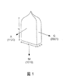
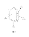
「r平面単結晶サファイア」とは、材料の主面に対して実質的に垂直である(±10度、通常は±1度)であるr軸を有する、実質的に平面の単結晶サファイアを意味する。図2を参照のこと。「サファイアr平面」というのは、当該技術分野において知られている通りであり、3つのサファイア平面[1−102]、[−1012]、および[01−12]の1つである。 “R-plane single crystal sapphire” refers to a substantially planar single crystal sapphire having an r-axis that is substantially perpendicular (± 10 degrees, usually ± 1 degree) to the major surface of the material. means. See FIG. The “sapphire r-plane” is as known in the art and is one of the three sapphire planes [1-102], [−1012], and [01-12].
「転位」は、本明細書において、当業者がそれを使用している通りに用いられており、Bragg回折に基づくx線回折トポグラフィを用いて検出可能である結晶欠陥を表わしている。 “Dislocations” are used herein as those skilled in the art are using them and represent crystal defects that can be detected using x-ray diffraction topography based on Bragg diffraction.
「リネージ」は、多結晶性の1形態であり、成長方向に対して低い誤配位角を有する1つの結晶内部の1つまたは複数の結晶粒である。この誤配位角は、典型的には2度未満であるが、それより大きいものでもあり得る。リネージは、結晶の全長さまたはその大部分を走行する列または行内に通常拘束されている多結晶性の一形態である。一部の条件下では、リネージは組織度が低くなるかもしれず、また全体的多結晶性へと崩壊するかもしれない。リネージを示す結晶は、数多くの利用分野において、特にチップ製造のために使用される場合またはサファイアが結晶成長のための基板または鋳型として使用される場合には、典型的に望ましいものではない。リネージはx線トポグラフィを用いて検出可能である。 “Lineage” is one form of polycrystallinity, and is one or more crystal grains within one crystal having a low misorientation angle with respect to the growth direction. This misorientation angle is typically less than 2 degrees, but can be larger. Lineage is a form of polycrystallinity that is usually constrained within columns or rows that run the full length of the crystal or most of it. Under some conditions, lineage may be less organized and may decay to overall polycrystallineness. Crystals exhibiting lineage are typically not desirable in many applications, particularly when used for chip manufacture or when sapphire is used as a substrate or mold for crystal growth. Lineage can be detected using x-ray topography.
結晶リボンの「スプレッド」は、当業者にとって公知の用語であり、リボンが最大幅に達する前に形成されるリボンの最初の部分である。それは典型的には種結晶における狭い部分から開始し、最大幅に達するまで幅が増大する。 The “spread” of a crystalline ribbon is a term known to those skilled in the art and is the first part of a ribbon that is formed before the ribbon reaches its maximum width. It typically starts from a narrow portion in the seed crystal and increases in width until the maximum width is reached.
「熱勾配」とは、単結晶サファイア生産装置内の2つの場所の間の距離にわたる平均的温度変化を意味する。2つの場所の間の距離は、生産プロセス中に単結晶サファイアがそれに沿って前進するライン上で測定される。例えば、縁端限定膜供給成長技術においては、炉内の第1の位置と炉内の第2の位置の間の温度差は摂氏50度であってよい。熱勾配の単位は、例えば「cmあたりの度数」または「インチあたりの度数」であってよい。特に規定されていない場合、温度変化は、サファイア結晶が勾配を通って第1の場所から第2の場所まで通過するにつれて、高温から低温に向かう。 “Thermal gradient” means the average temperature change over the distance between two locations in a single crystal sapphire production apparatus. The distance between the two locations is measured on a line along which the single crystal sapphire advances during the production process. For example, in the edge limited film feed growth technique, the temperature difference between the first position in the furnace and the second position in the furnace may be 50 degrees Celsius. The unit of thermal gradient may be, for example, “degrees per cm” or “degrees per inch”. Unless otherwise specified, the temperature change goes from high temperature to low temperature as the sapphire crystal passes through the gradient from the first location to the second location.
「リボン」とは、成形結晶成長技術を用いて形成されたプレートを意味する。 “Ribbon” means a plate formed using a shaped crystal growth technique.
縁端限定膜供給成長技術を用いて、単結晶サファイアの均一なa平面シートを効率良く生産できるということが示されてきた(米国特許出願公開第2005/0227117号明細書を参照のこと)。しかしながら、r平面シートは典型的には、例えばCzochralski法を用いて異なる成長配向に沿って成長させられるブールからスライスされる。ブールはさまざまな形状を有することができ、異なるブール内に異なるr軸配向が存在するような形に配向することができる。ウェーハを製造するためには、所望の直径の円筒をブールから切取り、例えば円筒の直径を通るワイヤーソースライシングを用いることで所望のウェーハを円筒から切断してよい。切断後、スライスを典型的には切削し研磨して、r平面ウェーハを生産する。最初にスライスを予め選択された幅に切断し、次に所望の寸法までラップ仕上げすることによりウェーハの厚みを選択してよい。ブールからプレートまたはウェーハを形成するのにこの生産方法を使用すると、各シートまたはウェーハはその主面に沿って少なくとも1回切断しなくてはならない。単結晶サファイアの硬度が極端に高いことは、切断ステップにコストおよび時間がかかり得ることを意味している。追加の準備ステップも必要となるかもしれない。その上、さらに大きいサイズのウェーハ例えば直径が5cmまたは10cm以上のウェーハの生産は、一部には二次および三次作業に起因して数週間を必要とする可能性がある。 It has been shown that uniform a-plane sheets of single crystal sapphire can be efficiently produced using edge-limited film feed growth techniques (see US Patent Application Publication No. 2005/0227117). However, r-plane sheets are typically sliced from boules that are grown along different growth orientations using, for example, the Czochralski method. The boules can have a variety of shapes and can be oriented such that there are different r-axis orientations within different boules. To manufacture a wafer, a desired diameter cylinder may be cut from the boule and the desired wafer may be cut from the cylinder, for example, using wire source slicing through the diameter of the cylinder. After cutting, the slice is typically cut and polished to produce an r-plane wafer. The wafer thickness may be selected by first cutting the slice to a preselected width and then lapping to the desired dimensions. Using this production method to form plates or wafers from boules, each sheet or wafer must be cut at least once along its major surface. The extremely high hardness of single crystal sapphire means that the cutting step can be costly and time consuming. Additional preparatory steps may also be required. Moreover, the production of larger sized wafers, for example wafers with a diameter of 5 cm or more than 10 cm, may require several weeks due in part to secondary and tertiary operations.
シートまたはリボンの形で形成されたr平面単結晶サファイアはこれらの準備ステップの多くを削減または短縮することができ得る。これらの様々な理由から、優れた光学特性および低いリネージを示すr平面シートは、r平面単結晶サファイアの好適な供給源を提供する可能性がある。 An r-plane single crystal sapphire formed in the form of a sheet or ribbon can reduce or shorten many of these preparation steps. For these various reasons, r-plane sheets that exhibit excellent optical properties and low lineage may provide a suitable source of r-plane single crystal sapphire.
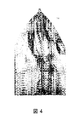
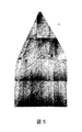
C−PLANE SAPPHIRE METHOD AND APPARATUSという名称の米国特許出願第11/858949号明細書中で記載されている通りのC平面材料用のEFG技術を使用してr平面リボンを製造することができる。可視光下ではこれらのリボンには欠陥がないように見える。しかしながら、x線トポグラフィは、リボンの一定長を走行する広範なリネージを明らかにしている。図2を参照のこと。 R-plane ribbons can be made using EFG technology for C-plane materials as described in US patent application Ser. No. 11 / 858,949, entitled C-PLANE SAPPHIRE METHOD AND APPARATUS. Under visible light, these ribbons appear to be free of defects. However, x-ray topography reveals extensive lineage that travels a certain length of ribbon. See FIG.
一実施形態においては、内部で冷却速度が具体的に制御されている2つ以上の冷却領域内にリボンを通過させるステップを含む成形結晶成長技術を用いて、リネージの不在を示すr平面単結晶サファイアリボンを成長させることができる。 In one embodiment, an r-plane single crystal exhibiting the absence of lineage using a shaped crystal growth technique that includes passing a ribbon through two or more cooling zones with cooling rates specifically controlled therein. Sapphire ribbon can be grown.
従来のEFG技術を用いて成長させたr平面リボンは、多くの場合、SOSチップの生産にとって適切であると考えられる完全結晶であると思われる。しかしながら、この技術を用いて成長させたウェーハは、SOSチップの生産には適していないことが判明した。リボンのx線トポグラフ解析後、リボンが多くのリネージを含むことがわかった。その上、ウェーハがSOSチップ生産に適していないのは、このリネージのためである。したがって、リネージの無いr平面単結晶サファイアを生産する方法は、現行の従来技術の大幅な改善であると思われる。 R-plane ribbons grown using conventional EFG technology often appear to be perfect crystals that are considered suitable for the production of SOS chips. However, it has been found that wafers grown using this technique are not suitable for the production of SOS chips. After x-ray topographic analysis of the ribbon, it was found that the ribbon contained a lot of lineage. Moreover, it is this lineage that makes the wafers unsuitable for SOS chip production. Therefore, the method of producing r-plane single crystal sapphire without lineage appears to be a significant improvement over current prior art.
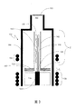
図3は、r平面リボンを生産するために用いられる装置100の横断面図を提供している。絶縁性加熱器144は、誘導コイル150および152によりひき起こされるPF場と結合するグラファイトなどの耐熱材料で作られていてよい。この装置は、溶融Al2O3であってよいメルトを保持するため、るつぼ110などのメルト供給源を含む。熱は、エンクロージャ144およびるつぼ110の両方の中で生成されてよい。るつぼは、メルトを収納できるあらゆる材料でできていてよい。アルミナは、バッチ式または連続式にるつぼに補給されてよい。るつぼ構造に適した材料は、例えばイリジウム、モリブデン、タングステンまたはモリブデン/タングステン合金である。モリブデン/タングステン合金は、組成がモリブデン0%から100%まで変動し得る。キャピラリーダイ120は、メルトと流体接触しており、メルトを引抜くことのできる3つのダイ先端部を含んでいる。3つのダイ先端部が示されているが、任意の数を使用してよい。外部ダイ先端部122および内部ダイ先端部124は、各々リボン130を同時に引抜く時に通すことのできる開口部を含む。外部ダイ先端部122は、内部ダイ先端部124よりも約0.020インチ高いところに位置づけしてよい。この差は、各々のダイ先端部およびリボンが曝露されている温度プロフィールを等化するのに役立つかもしれない。図3に示されている通りのダイ先端部は典型的にその縁端で中心部分よりも温かい。リボンが形成されるにつれ、熱の大部分が、リボンを通した放射線チャネリングを介して失われると考えられている。したがって、リボンが広くなるほど、この機構によってより多くの熱が失われる可能性がある。
FIG. 3 provides a cross-sectional view of an
図3に示されている図は、各リボンの厚みを示す端面図である。リボンの厚みは、少なくとも一部には、ダイ先端部の幅に基づいている。図3中の左から右に向かって、ダイ先端部の深さ(ダイ先端部の最短寸法)は、生産されるリボンの厚みを決定するように選択されてよい。ダイの深さは、例えば約0.1、0.2、0.5または1.0センチメートル以上であってよい。ダイの幅(図3中の図は、ダイ先端部の幅に沿って見たものである)はリボンの幅を決定し、例えば10cm、15cm、20cm、25cm以上であってよい。したがって、0.5cmの深さおよび20cmの幅を有するダイ先端部は、およそ0.5cmの厚みとおよそ20cmの幅を有するリボンを生産し得る。ダイ先端部の寸法は、メルトをダイ先端部に補給するキャピラリー開口部の寸法とは無関係である。引抜くことのできるリボンの長さは、空間的要件および取扱いの容易さなどの実施上の配慮点によって制限を受ける。別段の規定のないかぎり、リボンの長さは、ネック部(リボンが播種される狭くなった箇所)から反対側の端部まで測定される。 The view shown in FIG. 3 is an end view showing the thickness of each ribbon. The ribbon thickness is based at least in part on the width of the die tip. From left to right in FIG. 3, the depth of the die tip (the shortest dimension of the die tip) may be selected to determine the thickness of the ribbon to be produced. The depth of the die may be, for example, about 0.1, 0.2, 0.5, or 1.0 centimeter or more. The width of the die (the view in FIG. 3 is viewed along the width of the die tip) determines the width of the ribbon and may be, for example, 10 cm, 15 cm, 20 cm, 25 cm or more. Thus, a die tip having a depth of 0.5 cm and a width of 20 cm can produce a ribbon having a thickness of approximately 0.5 cm and a width of approximately 20 cm. The size of the die tip is independent of the size of the capillary opening that refills the die tip. The length of the ribbon that can be drawn is limited by practical considerations such as spatial requirements and ease of handling. Unless otherwise specified, the length of the ribbon is measured from the neck (the narrow spot where the ribbon is seeded) to the opposite end.
結晶化が発生するにつれて、熱は伝導、対流および放射を通してサファイアリボンから失われ得る。熱は、例えば加熱器144およびるつぼ110を誘導結合することによってかまたはシステムを抵抗加熱することによって、システムに供給され得る。加熱ゾーン1(z1)の中に遮熱材140が位置づけされ、これは、リボンが形成後に放射し始めた時に失われる熱を減少させるのに役立つ。リボンからの熱損失を削減するのに役立つように、断熱容器142を設計してよい。この容器は、ゾーン2(z2)に熱を供給するべく上部rf誘導コイル152に誘導結合できるモリブデンなどの高温材料で作られていてよい。ゾーン1内では、遮熱材140および断熱容器が、リボンがその最高温度にある領域内での熱損失を減少させるのに役立つ。RF誘導コイル150は、連続したコイルであっても、連続したコイルでなくてもよい。RF誘導コイル150および152は、2つの別々のコイルであってよく、独立して制御されてよい。
As crystallization occurs, heat can be lost from the sapphire ribbon through conduction, convection and radiation. Heat can be supplied to the system, for example, by inductively coupling the
扉160は、エンクロージャの上面において開口部162の一部分を少なくとも被覆し、熱損失を削減しかつ気体流を誘導して結果として熱勾配を改変し得る。アルゴンなどの不活性ガスを典型的には装置内に流入させて酸化を制限するのを助ける。この気体流はシステムから熱を取除くことができ、気体流の量が減少すると、システムから失われる熱の量も同様に減少する。扉160は、本来であれば放射や対流を通して失われると思われる熱損失を防止し得る。扉は例えば単一の扉または二重跳上げ戸であってよく、開口部162を通して引き上げられるにつれてリボンを通過させるべく開放できるような形でヒンジ留めされていてよい。一部の実施形態では、扉は開口面積の50%超、75%超、または90%超を覆っているか、またはそのように調整されていてよい。
The
EFG装置100には、ダイ先端部におけるリボンの形成の視覚的監視を可能にするように位置づけされた2つのビューポートを備えることができる。これらのビューポートのサイズは約0.22×0.66インチであってよい。しかしながら、ビューポートのサイズを約0.15×0.75インチまで削減すると、熱損失はかなり減少し、温度勾配の制御が向上する結果となる。
The
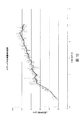
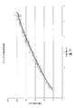
これらの変更を伴うおよび伴わない熱損失の比較が図6、7および8に示されている。図6は、能動第2段熱源が欠如し、標準サイズのビューポートならびに開放上面を含む装置(A)内の垂直方向温度勾配のグラフ表示を提供している。図7は、能動第2段熱源を使用しかつ標準サイズのビューポートならびに開放上面を含む装置(B)内の垂直方向温度勾配のグラフ表示を提供している。図8は、煙突の上面で開口部を被覆する旋回可能な跳上げ戸およびさらに小さいビューポートを伴う改良型装置(C)内の垂直方向温度勾配のグラフ表示を提供する(図3を参照のこと)。温度測定は、リボン成長をシミュレートする条件下で熱電対を使用し、ただし実際にリボンを引抜くことなく行なわれている。 A comparison of heat loss with and without these changes is shown in FIGS. FIG. 6 provides a graphical representation of the vertical temperature gradient in device (A) that lacks an active second stage heat source and includes a standard size viewport as well as an open top surface. FIG. 7 provides a graphical representation of the vertical temperature gradient in device (B) using an active second stage heat source and including a standard size viewport as well as an open top surface. FIG. 8 provides a graphical representation of the vertical temperature gradient in an improved device (C) with a swivel door that covers the opening at the top of the chimney and a smaller viewport (see FIG. 3). about). Temperature measurements are made using a thermocouple under conditions that simulate ribbon growth, but without actually pulling out the ribbon.
図6は、装置A内のダイ先端部とダイ先端部より上の最初の2分の1インチの間で摂氏40度超の初期降下を示す。第2段熱源を伴う装置Bからの結果を提供する図7は、ダイ先端部とダイ先端部より上最初の2分の1インチの間で摂氏30度の初期降下を示している。その後温度は、実際には約1インチの間上昇し、次にダイ先端部より5インチ上で摂氏約100度の正味降下まで下降する。温度上昇は、第2段熱源の使用に起因するものと考えられている。図8にデータを提供している装置Cでは、最初の2分の1インチにおける初期降下は、20度未満であり、最初の6インチにわたる合計降下は80度未満である。ここでも同様に、リボンが2分の1インチレベルから2インチレベルまで移動するにつれて温度ははるかに小さい上昇または無視できる程度の上昇しか示さない。装置Bは、2インチから6インチまでの範囲にわたり1インチあたり約20℃の温度勾配を示す。しかしながら、装置Cは、対応する領域内で1インチあたり約14℃の温度勾配を示す。
FIG. 6 shows an initial drop of over 40 degrees Celsius between the die tip in Device A and the first half inch above the die tip. FIG. 7, which provides results from Device B with a second stage heat source, shows an initial drop of 30 degrees Celsius between the die tip and the first half inch above the die tip. The temperature then actually rises for about 1 inch and then falls to a net drop of about 100
図7のプロフィールは、図4のx線トポグラフの中で示された幅6インチのr平面リボンを生産するために使用されてきた。広範囲のリネージがトポグラフ内に明らかに見える。これは、図8の勾配プロフィールを用いて幅6インチのr平面リボンを成長させ、リネージの無い図5のトポグラフと対照的である。これらの低い方の温度勾配は、リボン内部の応力を減少させ、スリップを削減し、リネージの少ないまたはリネージの無いプレートを提供するのに役立つと考えられている。 The profile of FIG. 7 has been used to produce the 6-inch wide r-plane ribbon shown in the x-ray topograph of FIG. A wide range of lineage is clearly visible in the topograph. This is in contrast to the topograph of FIG. 5 where a 6-inch wide r-plane ribbon is grown using the gradient profile of FIG. These lower temperature gradients are believed to help reduce stress inside the ribbon, reduce slip, and provide a plate with less or no lineage.
一態様においては、リネージの無いr平面サファイアリボンを成長させるための方法が提供されている。図3に提供されている装置を用いた方法の一実施形態においては、るつぼ110にアルミナを充填し誘導結合された加熱用コイル150を用いて2060℃まで加熱することによって、Al2O3のメルトが提供される。r平面[1−102]が図3で左(または右)を向いているように、各ダイ先端部の開口部にサファイア種結晶が設置される。種結晶はダイ先端部の上面でメルトと接触させられ、上に引き上げられてスプレッドを開始する。引抜きの方向は、結晶の方向[1−10−1]と同じ方向である。このとき、1時間あたり約1インチ、約0.5インチ、約2インチまたは2インチ超などの適切な速度で、種結晶を上に引抜くことができる。
In one aspect, a method is provided for growing a lineage-free r-plane sapphire ribbon. In one embodiment of the method using the apparatus provided in FIG. 3, the
公知のEFG方法においては、スプレッドは典型的には、最大幅が達成されるまで最大速度すなわち最大重量増加速度で形成される。こうして、最大幅に到達するのに必要な時間が短縮され、スプレッド中に形成する比較的価値の低い結晶材料(幅が比較的小さいことを理由とする)の量が減少する。重量増加量を測定するために、種結晶を保持する支持体は、オペレータが選択する任意の間隔でリボンの重量を測定できるロードセルに接続されている。例えば、重量を毎秒測定し記録することができる。一定の引抜き速度では、スプレッドが大きくなるにつれて、最大幅が得られるまで重量増加速度は増大することがわかる。 In known EFG methods, the spread is typically formed at the maximum speed, i.e. the maximum weight gain rate, until the maximum width is achieved. This reduces the time required to reach the maximum width and reduces the amount of relatively low value crystalline material (because of the relatively small width) that forms in the spread. To measure the weight gain, the support holding the seed crystal is connected to a load cell that can measure the weight of the ribbon at any interval selected by the operator. For example, the weight can be measured and recorded every second. It can be seen that at a constant drawing speed, the weight increase rate increases as the spread increases until the maximum width is achieved.
一般に、ダイ先端部における温度が低くなるほど、結晶化は速くなり、ひいては重量増加速度は速くなりかつより短いスプレッドがより急速に最大幅に達することになる。しかしながら、ダイ先端部(メルト界面)における温度が過度に低い場合、メルトはダイと接触して結晶化し、その結果リボンは役に立たなくなる。スプレッドが大きくなるにつれて、展開するリボンからより多くの熱量が失われ、その結果メルト界面により低い温度がもたらされる。温度補償を目的として、メルト界面において温度を維持するためにRFコイル150から付加的な電力を供給することができる。
In general, the lower the temperature at the die tip, the faster the crystallization, and hence the faster the rate of weight increase, and the shorter spread will reach its maximum width more quickly. However, if the temperature at the die tip (melt interface) is too low, the melt will crystallize in contact with the die, resulting in a useless ribbon. As the spread increases, more heat is lost from the developing ribbon, resulting in a lower temperature at the melt interface. For the purpose of temperature compensation, additional power can be supplied from the
ダイに対する凍結無くスプレッド速度を最大限にするため、以下の手順が開発され、a平面無欠陥単結晶サファイア上でうまく使用された。ダイ先端部近くのるつぼのフタの上に温度読取りを行なうために設置されたパイロメータを用いて、間接的に熱が測定される。最初に、メルトを摂氏2053度より高い温度にセットし、種結晶をメルト界面でメルトと接触させる。結晶化が開始してから、引抜き中の特定のリボンについて適切な速度で引抜きが開始される。スプレッドの重量増加は頻繁に、例えば毎秒、監視される。スプレッドが大きくなり、付加的な冷却がダイ先端部において発生するにつれて、ロードセルは、結晶化がダイ表面に近づくにつれて発生するメルト内の粘度増加に起因し得る重量増加スパイクを検出することができる。コントローラーはこの突然の負荷増加(1〜10秒にわたる)を検出した時点で、パイロメータにおける温度が摂氏1度だけ上昇するまでRFコイル150への電力を増大させ、次に別の突然の負荷増加が検出されるまでこの設定値を維持する。増加が再び検出された時点で、プロセスを反復し、温度を摂氏1度だけ上昇させる。このようにして、リボンを損傷することなく、また欠陥を形成することなく、最大速度でリボンをスプレッドさせることができる。この手順にしたがった場合、スプレッド中の重量増加速度は成長期間中の任意の点でその最大値にあると考えられており、この増加速度は「最大重量増加速度」と呼ばれる。この重量増加速度を超えた場合、ダイと接触した結晶化に起因してリボンが不良になる結果がもたらされる確率が高い。
In order to maximize spread speed without freezing on the die, the following procedure was developed and successfully used on a-plane defect-free single crystal sapphire. Heat is measured indirectly using a pyrometer installed to take a temperature reading on the crucible lid near the die tip. First, the melt is set to a temperature above 2053 degrees Celsius and the seed crystal is brought into contact with the melt at the melt interface. After crystallization has begun, drawing begins at the appropriate speed for the particular ribbon being drawn. Spread weight gain is monitored frequently, eg every second. As the spread increases and additional cooling occurs at the die tip, the load cell can detect weight gain spikes that can be attributed to increased viscosity in the melt as crystallization approaches the die surface. When the controller detects this sudden load increase (over 1-10 seconds), it increases the power to the
この最大重量増加速度を用いて、a平面サファイアを生産することができるが、このスプレッド形成方法を用いて生産させたr平面リボンは、たとえリボンが裸眼には欠陥の無いものに見えてもリネージを発生させる結果になる。さらに、r平面材料がより温かいスプレッド相から恩恵を受けること、そして重量増加速度を最大重量増加速度より低く保った場合リネージの無いr平面リボンを生産できることも発見されてきた。 Although this maximum weight gain rate can be used to produce a-plane sapphire, r-plane ribbons produced using this spread forming method are lineage even if the ribbon appears to be free of defects to the naked eye. Result. In addition, it has also been discovered that r-plane materials can benefit from a warmer spread phase and that lineage-free r-plane ribbons can be produced if the weight gain rate is kept below the maximum weight gain rate.
最大重量増加速度でスプレッドを形成させる代りに、最大速度の90%未満、80%未満または70%未満でスプレッドを形成させた結果としてリネージの無いリボンひいてはウェーハをもたらすことができるということが発見された。スプレッドの開始時における重量増加速度は、リボンの幅が非常に小さい場合百分率として可変的であることから、一般にこれは無視されるべきである。典型的には、重量増加速度を計算するのにスプレッド形成の最初の2分の1インチは使用されず、別段の規定のないかぎり、本明細書ではスプレッドの幅の最初の2分の1インチは、重量増加速度を考慮する際に無視されるべきである。 It has been discovered that instead of forming the spread at the maximum weight gain rate, forming the spread at less than 90%, less than 80% or less than 70% of the maximum speed can result in a ribbon and thus a wafer without lineage. It was. This should generally be ignored as the rate of weight increase at the beginning of the spread is variable as a percentage when the ribbon width is very small. Typically, the first half inch of the spread formation is not used to calculate the rate of weight increase, and unless otherwise specified, the first half inch of the width of the spread is used herein. Should be ignored when considering the rate of weight increase.
x線トポグラフィを用いてリネージが全く見られない場合、r平面サファイアプレートはリネージが無いものとみなされる。多結晶性および転位などの特徴が存在している場合でも、r−平面プレートはなおリネージが無い状態であり得る。リネージを示すリボンのx線トポグラフが図4に提供されている。典型的に見出されるように、リネージはリボンのほぼ全長にわたり中心にある。リネージの無いリボンのx線トポグラフが図5に提供されている。 If no lineage is seen using x-ray topography, the r-plane sapphire plate is considered free of lineage. Even when features such as polycrystallinity and dislocations are present, the r-plane plate may still be free of lineage. A ribbon x-ray topograph showing lineage is provided in FIG. As typically found, the lineage is centered over almost the entire length of the ribbon. An x-ray topograph of a ribbon without lineage is provided in FIG.
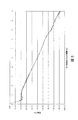
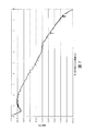
図10および11中に、重量増加速度対引張り長さの関係を示す2つのグラフが提供されている。図10は、上述の通りの最大重量増加速度を示す。図11は、重量増加速度が最大速度の80%未満に維持されている制御された重量増加速度を示している。両データセット共に、一時間あたり1インチの引張り速度で生成された。図11の平滑な曲線を、指数方程式y=axbに当てはめることができ、ここでy=は重量増加速度、xは引張り長さであり、係数aおよびbは組合わさってスプレッドの長さおよび角度を制御する。好ましくは、データはこの指数方程式に当てはまり、最小二乗回帰解析を用いて0.95超または0.97超のr2値を示す。この高いr2値は、重量増加速度の増大において最小限の急上昇または降下しか示さない平滑な成長速度を表わしている。一実施形態においては、リネージの無いr平面材料を生産するための標的重量増加速度はy=32x0.65である。指数関数に当てはめるのではなくむしろ、最大成長速度を示す曲線中のデータ(図10)は、対数方程式y=34ln(x)+48を用いて最もうまくモデリングされる。 In FIGS. 10 and 11, two graphs are provided that show the relationship between the rate of weight increase versus the tensile length. FIG. 10 shows the maximum weight increase rate as described above. FIG. 11 shows a controlled weight gain rate where the weight gain rate is maintained below 80% of the maximum speed. Both data sets were generated at a pull rate of 1 inch per hour. The smooth curve of FIG. 11 can be fitted to the exponential equation y = ax b , where y = weight increase rate, x is the tensile length, and the coefficients a and b are combined to determine the spread length and Control the angle. Preferably, the data fits this exponential equation and shows an r 2 value greater than 0.95 or greater than 0.97 using least squares regression analysis. This high r 2 value represents a smooth growth rate with minimal jump or drop in increasing weight gain rate. In one embodiment, the target weight increase rate to produce lineage-free r-plane material is y = 32 × 0.65 . Rather than fitting to an exponential function, the data in the curve showing the maximum growth rate (FIG. 10) is best modeled using the logarithmic equation y = 34ln (x) +48.
その他の実施形態においては、スプレッドの重量増加速度は、そのスプレッドの先行部分における重量増加速度に対して制限されてよい。例えば長さの1インチ増加中の重量増加速度は、同じリボン内の任意の先行する1インチの成長長さの間の重量増加速度の例えば150%以下、200%以下または250%以下であってよい。 In other embodiments, the weight increase rate of the spread may be limited relative to the weight increase rate in the leading portion of the spread. For example, the rate of weight increase during a 1 inch increase in length is, for example, 150% or less, 200% or less, or 250% or less of the weight increase rate during any preceding 1 inch growth length in the same ribbon. Good.
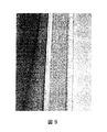
リネージを伴うリボンと伴わないリボンの比較は、裸眼では困難である。しかしながら、制御された重量増加速度の別の効果を視覚的に見ることが可能であり、これは、最大重量増加速度(図9右側)でおよび最大重量増加速度の80%未満の制御された重量増加速度(図9の左側)で成長させたr平面リボンの縁端を示す図9の中で示されている。より制御された重量増加速度が使用された場合に、はるかに平滑な縁端(図9の左側)が発達するということは明らかである。数多くの最終製品はリボンから切断されることから、縁端の質は典型的には監視されないが、縁端が平坦であるほど少ない応力が示されることがあり、これは、より少ないスリップおよび/またはより少ないリネージを結果としてもたらすかもしれない。 Comparison of ribbons with and without lineage is difficult with the naked eye. However, it is possible to visually see another effect of a controlled weight gain rate, which is a controlled weight at the maximum weight gain rate (right side of FIG. 9) and less than 80% of the maximum weight gain rate. The r-plane ribbon edge grown at an increasing rate (left side of FIG. 9) is shown in FIG. It is clear that a much smoother edge (left side of FIG. 9) develops when a more controlled weight gain rate is used. Because many end products are cut from the ribbon, the edge quality is typically not monitored, but the flatter the edge, the less stress may be shown, which means less slip and / or Or it may result in less lineage.
別の態様においては、r平面単結晶サファイアは、結晶化されたリボンの冷却速度を制御するEFG技術を用いて生産可能である。一組の実施形態において、これは、2つの全く異なる冷却ゾーンを含んでいてよい。EFG法により単結晶サファイアを生産するのに使用される公知のシステムは、典型的に、メルト界面の直ぐ下流側の領域内で1インチあたり100℃超の垂直方向温度勾配を使用する。このことはすなわち、点aから点bまでサファイアリボン上の1点が下流側で1インチ(通常は垂直方向上へ)前進するにつれて、点bにおける温度はそれが点aにあった時よりも100℃低くなることを意味している。これは同様に、リボンが上向きに1インチ引抜かれるにつれて約100℃だけ冷却し、1時間あたり1インチで引抜かれるのであれば、それに約1時間かかるということも意味している。リボン温度は、生産中に直接測定するのが困難であることから、これらの値は通常、リボンが存在しない状態でとられた温度測定値から補間される。 In another aspect, r-plane single crystal sapphire can be produced using EFG technology that controls the cooling rate of the crystallized ribbon. In one set of embodiments, this may include two completely different cooling zones. Known systems used to produce single crystal sapphire by the EFG method typically use a vertical temperature gradient of more than 100 ° C. per inch in the region immediately downstream of the melt interface. This means that as one point on the sapphire ribbon advances 1 inch downstream (usually vertically upward) from point a to point b, the temperature at point b is greater than when it was at point a. It means that the temperature is lowered by 100 ° C. This also means that if the ribbon is cooled by about 100 ° C. as it is drawn 1 inch upward, it will take about 1 hour if it is drawn at 1 inch per hour. Since ribbon temperature is difficult to measure directly during production, these values are usually interpolated from temperature measurements taken in the absence of the ribbon.
約1850℃より高い温度において、サファイア結晶の冷却速度の制御がその結晶品質に影響を及ぼすかもしれないということが判明した。例えば、過度に急速に冷却された場合、1つの結晶平面の別の結晶平面上への「スリップ」が発生し、リネージを導くかもしれない。冷却を調節することによって制御可能な別のタイプの結晶欠陥は、転位である。結晶の温度が約1850℃より低く下降してから、それはより安定した単結晶構造の結晶となり得、冷却速度を入念に調節する必要はないかもしれない。例えば、結晶がその脆性−延性遷移点より低温で装置から退出する場合、結晶に対する不可逆的損傷が全くない状態で、結晶を高速で室温まで冷却できるかもしれない。 It has been found that at temperatures above about 1850 ° C., controlling the cooling rate of the sapphire crystal may affect its crystal quality. For example, if cooled too quickly, a “slip” of one crystal plane onto another crystal plane may occur, leading to lineage. Another type of crystal defect that can be controlled by adjusting cooling is a dislocation. After the temperature of the crystal drops below about 1850 ° C., it can become a more stable single crystal crystal and the cooling rate may not need to be carefully adjusted. For example, if the crystal exits the device at a temperature below its brittle-ductile transition point, it may be possible to cool the crystal to room temperature at high speed without any irreversible damage to the crystal.
リボン生産が開始したら勾配を一定の値に維持することが好ましいかもしれないが、装置内の任意の特定の場所において熱勾配を変動させてよい。ただし、プロセスパラメータの変動を補償するかまたはリボンの品質を改善するために、生産中勾配を調整してもよい。熱勾配は、例えば、遮熱材を下降または上昇させること、断熱材を追加または除去すること、ビューポートのサイズを削減すること、装置の煙突部分に扉を追加すること、および/または装置の一部分または複数の部分を能動的に加熱または冷却することにより、熱勾配を制御してもよい。 Although it may be preferable to maintain the gradient at a constant value once ribbon production has begun, the thermal gradient may be varied at any particular location within the apparatus. However, the in-production slope may be adjusted to compensate for process parameter variations or to improve ribbon quality. Thermal gradients can, for example, lower or raise the heat shield, add or remove insulation, reduce the size of the viewport, add a door to the chimney portion of the device, and / or The thermal gradient may be controlled by actively heating or cooling the portion or portions.
熱勾配は、勾配の長さ全体にわたり実質的に一定であってよい。例えば、熱勾配は、2分の1インチ未満、2分の1インチ超、1インチ超、1.5インチ超、2インチ超、4インチ超、6インチ超または8インチ超の距離にわたり実質的に一定であってよい。熱勾配は同様に、勾配の長さにわたり、特に勾配の始まりおよび/または終りにおいて変動してもよい。当然のことながら、1つの勾配から別の勾配へと移行する場合、勾配が第1の勾配から第2の勾配までシフトする遷移距離が存在するかもしれない。別段の規定のないかぎり、一つの特定領域についての熱勾配は、その領域全体にわたる平均熱勾配である。 The thermal gradient may be substantially constant throughout the length of the gradient. For example, the thermal gradient is substantially over a distance of less than 1/2 inch, greater than 1/2 inch, greater than 1 inch, greater than 1.5 inch, greater than 2 inch, greater than 4 inch, greater than 6 inch, or greater than 8 inch. It may be constant. The thermal gradient may likewise vary over the length of the gradient, in particular at the beginning and / or end of the gradient. Of course, when transitioning from one gradient to another, there may be a transition distance where the gradient shifts from the first gradient to the second gradient. Unless otherwise specified, the thermal gradient for a particular region is the average thermal gradient across that region.
特定の引張り長さについてではなく時間の長さについて冷却を制御してもよい。例えば、結晶化後の形成の最初の一時間について、温度の低下を80℃未満、60℃未満、40℃未満または30℃未満に制限してよい。形成の最初の6時間について、温度の低下を例えば120℃未満、100℃未満、または80℃未満に制限してよい。結晶化の後2時間〜8時間の間、温度の低下を例えば140℃未満、120℃未満または100℃未満に制限してもよい。 Cooling may be controlled for a length of time rather than for a specific pull length. For example, for the first hour of formation after crystallization, the temperature drop may be limited to less than 80 ° C, less than 60 ° C, less than 40 ° C, or less than 30 ° C. For the first 6 hours of formation, the temperature drop may be limited to, for example, less than 120 ° C, less than 100 ° C, or less than 80 ° C. Between 2 and 8 hours after crystallization, the temperature drop may be limited to, for example, less than 140 ° C, less than 120 ° C, or less than 100 ° C.
図3の装置は、冷却速度を制御するために使用可能な2つの全く異なる冷却領域Z1およびZ2を含む。領域Z2は、この領域に対し能動的に熱を供給できる独立した加熱器を含む。図示された実施形態においては、誘導加熱コイル152は、モリブデンエンクロージャ142と結合されて、領域に能動的に熱を加える。これはリボンから外部環境へと失われた熱を補償するのに役立つ。熱の大部分がリボン自体により誘導される放射線を通して失われるということが発見された。この熱の多くは扉160を用いることで保持でき、2つのビューポート(図示せず)のサイズを縮小することでも熱損失を削減できるということも示された。扉160は同様に、エンクロージャ142の表面に沿った不活性ガス流の対流に起因して失われる熱の量を削減するのにも役立つかもしれない。これらの変更を実施すると、領域Z2内の温度勾配を1インチあたり20℃未満、18℃未満、16℃未満、または14℃未満となるように制御することができる。同様にして、典型的には2つのゾーンのうちの高温の方であるゾーンZ1における温度勾配を、従来のEFG勾配よりも小さい勾配を提供するように制御することも可能である。この制御は、少なくとも一部には、より小さいビューポートの実施、扉160の設置、遮熱材140の使用を通しておよび内部ダイ先端部124に対して外部ダイ先端部122の高さをずらして配置することによって達成可能である。メルト界面に隣接するゾーンZ1内で達成可能な有利な温度勾配は、1インチあたり100℃未満、80℃未満、60℃未満または40℃未満である。
The apparatus of FIG. 3 includes two completely different cooling zones Z 1 and Z 2 that can be used to control the cooling rate. Region Z 2 is to this region, including a separate heater can be supplied actively heat. In the illustrated embodiment,
以下の方法により、検出可能なリネージを全く示さない長さ18インチのr平面単結晶サファイアリボンを成長させた。 An 18-inch long r-plane single crystal sapphire ribbon that did not show any detectable lineage was grown by the following method.
図3の結晶成長装置を用いて、サファイア種結晶をそれぞれのダイ先端部の上部表面上でアルミナメルトと接触状態に置いた。ダイ開口部の幅(長い水平方向寸法)と面[1−102]を位置合わせさせた状態で種結晶を配向し、[1−10−1]方向に垂直方向に引張った。結晶化が進むにつれて、種結晶を1時間あたり1インチの速度で上向きに引抜いた。温かいスプレッドを生産するため、制御された重量増加のプログラムを実施し、制御された重量増加速度を最大重量増加速度の80%未満に保った。重量増加速度は図11に示されており、0.96というr2値で等式y=32×0.65に当てはまる。約6インチの引張り長さの後に最大リボン幅を達成した。 Using the crystal growth apparatus of FIG. 3, a sapphire seed crystal was placed in contact with the alumina melt on the upper surface of each die tip. The seed crystal was oriented in a state where the width of the die opening (long horizontal dimension) and the plane [1-102] were aligned, and pulled in the direction perpendicular to the [1-10-1] direction. As crystallization progressed, the seed crystal was drawn upward at a rate of 1 inch per hour. In order to produce a warm spread, a controlled weight gain program was implemented to keep the controlled weight gain rate below 80% of the maximum weight gain rate. The rate of weight increase is shown in FIG. 11 and applies to the equation y = 32 × 0.65 with an r 2 value of 0.96. Maximum ribbon width was achieved after a pull length of about 6 inches.
図8に示された温度プロフィールを再現するように装置を作動させた。リボンが装置の領域Z1を通して引張られるにつれて、垂直方向の温度勾配(中心にある)は1インチあたり約40℃未満に維持され、上向き方向で徐々に低温になった。領域Z1とZ2の間に、領域Z1の勾配から領域Z2の1インチあたり平均14℃の勾配まで温度勾配が減少する遷移ゾーンが存在する。Z1およびZ2を通して、リボンの温度を約1850℃超に維持した。より小さいビューポート、能動的な加熱そして断熱扉160の使用を通して、少なくとも部分的には、低い冷却速度を持続させることが可能である。
The apparatus was operated to reproduce the temperature profile shown in FIG. As the ribbon was pulled through zone Z1 of the device, the vertical temperature gradient (in the center) was maintained below about 40 ° C. per inch and gradually decreased in the upward direction. Between zones Z1 and Z2, there is a transition zone where the temperature gradient decreases from the slope of zone Z1 to an average of 14 ° C. per inch of zone Z2. Through Z1 and Z2, the ribbon temperature was maintained above about 1850 ° C. Through the use of smaller viewports, active heating and
1時間あたり1インチの引張り速度を、長さ18インチのリボンが得られるまで維持した。その後、結晶がダイから分離するまで、成長速度を増大させた。その後リボンをゆっくりと開口部162まで上へ移動させ、跳上げ戸160を開くことによりこの開口部162を通してとり出し、室温までの冷却を終了した。材料が脆性−延性遷移点より低く冷却してから、それを無制御の冷却速度に付してよいが、それでもなお幾分かの制御が望ましいかもしれない。リボンの一部分のx線トポグラフが図5に示されており、これがリネージの不在を表わしている。
A pulling speed of 1 inch per hour was maintained until an 18 inch long ribbon was obtained. Thereafter, the growth rate was increased until the crystals separated from the die. Thereafter, the ribbon was slowly moved up to the
本発明の複数の実施形態について本明細書中で記載し例示してきたが、当業者であれば、本明細書中に記述された機能を実施しかつ/または結果および/または利点のうちの1つ以上を得るためのさまざまなその他の手段および/または構造を容易に想定するものであり、かかる変形形態および/または修正の各々は本発明の範囲内に入るものとみなされる。より一般には、当業者であれば、本明細書に記載されている全てのパラメータ、寸法、材料および形態が例示的なものであるように意図されていること、そして実際のパラメータ、寸法、材料および/または形態が、本発明の教示を使用する具体的な1つまたは複数の利用分野によって左右されるものであることを容易に認識するものである。当業者であれば、単に日常的な実験を用いて、本明細書中で記載されている本発明の具体的実施形態に対する数多くの均等物を認識するかまたはそれを確認することができる。したがって、以上の実施形態はあくまでも一例として提示されていることそして、添付の特許請求の範囲およびその均等物の範囲内で、具体的に記載され権利請求された通りのもの以外の形で本発明を実施してもよいこと、を理解すべきである。本発明は、本明細書中で記載されている各々の個別の特徴、システム、物品、材料、キットおよび/または方法に関する。さらに、かかる特徴、システム、物品、材料、キットおよび/または方法が相互に整合性を有するものである場合、それらの特徴の2つ以上の任意の組合せが本発明の範囲内に入る。 Although multiple embodiments of the present invention have been described and illustrated herein, one of ordinary skill in the art will perform the functions described herein and / or one of the results and / or advantages. Various other means and / or structures for obtaining one or more are readily envisioned and each such variation and / or modification is considered to be within the scope of the invention. More generally, those skilled in the art will recognize that all parameters, dimensions, materials and forms described herein are intended to be exemplary and that the actual parameters, dimensions, materials It will be readily appreciated that and / or form will depend on the specific field or fields of application using the teachings of the invention. Those skilled in the art will recognize, or be able to ascertain using no more than routine experimentation, many equivalents to the specific embodiments of the invention described herein. Accordingly, the foregoing embodiments have been presented by way of example only and, within the scope of the appended claims and their equivalents, other than as specifically described and claimed. It should be understood that may be implemented. The present invention is directed to each individual feature, system, article, material, kit, and / or method described herein. Further, where such features, systems, articles, materials, kits and / or methods are compatible with each other, any combination of two or more of those features is within the scope of the invention.
本明細書中で定義され使用されている通りの全ての定義は、辞書の定義、本明細書に参照により援用されている文献中の定義および/または定義された用語の通常の意味に優先するものであると理解されるべきである。 All definitions as defined and used herein take precedence over dictionary definitions, definitions in the literature incorporated by reference herein, and / or the ordinary meaning of the defined terms. Should be understood to be.
本明細書中および特許請求の範囲中で使用されている不定冠詞「a」および「an」は、明らかに相反する指示のないかぎり、「少なくとも1つ」を意味するものとして理解されるべきである。 The indefinite articles “a” and “an” as used herein and in the claims are to be understood as meaning “at least one” unless clearly indicated to the contrary. is there.
本出願中で引用または参照されている全ての参考文献、特許および特許出願そして刊行物は、その全体が本明細書に参照により援用されるものである。 All references, patents and patent applications and publications cited or referenced in this application are hereby incorporated by reference in their entirety.
Claims (2)
前記リネージの不在が、Bragg回折に基づくx線回折トポグラフィを用いて、示されるr平面単結晶サファイアウェーハ。 Have a diameter of more than 200 mm, Ri Ah with r-plane single crystal sapphire wafer showing the absence of lineage is a form of polycrystalline,
An r-plane single crystal sapphire wafer in which the absence of lineage is indicated using x-ray diffraction topography based on Bragg diffraction .
Applications Claiming Priority (5)
| Application Number | Priority Date | Filing Date | Title |
|---|---|---|---|
| US98975607P | 2007-11-21 | 2007-11-21 | |
| US60/989,756 | 2007-11-21 | ||
| US12/274,593 | 2008-11-20 | ||
| US12/274,593 US20090130415A1 (en) | 2007-11-21 | 2008-11-20 | R-Plane Sapphire Method and Apparatus |
| PCT/US2008/084277 WO2009067641A2 (en) | 2007-11-21 | 2008-11-21 | R-plane sapphire method and apparatus |
Publications (2)
| Publication Number | Publication Date |
|---|---|
| JP2011504451A JP2011504451A (en) | 2011-02-10 |
| JP5513402B2 true JP5513402B2 (en) | 2014-06-04 |
Family
ID=40642277
Family Applications (1)
| Application Number | Title | Priority Date | Filing Date |
|---|---|---|---|
| JP2010535082A Expired - Fee Related JP5513402B2 (en) | 2007-11-21 | 2008-11-21 | r-plane single crystal sapphire wafer |
Country Status (5)
| Country | Link |
|---|---|
| US (3) | US20090130415A1 (en) |
| JP (1) | JP5513402B2 (en) |
| RU (1) | RU2448204C2 (en) |
| TW (2) | TWI404842B (en) |
| WO (1) | WO2009067641A2 (en) |
Families Citing this family (30)
| Publication number | Priority date | Publication date | Assignee | Title |
|---|---|---|---|---|
| US7348076B2 (en) | 2004-04-08 | 2008-03-25 | Saint-Gobain Ceramics & Plastics, Inc. | Single crystals and methods for fabricating same |
| US20100101387A1 (en) * | 2008-10-24 | 2010-04-29 | Kedar Prasad Gupta | Crystal growing system and method thereof |
| US20110179992A1 (en) * | 2008-10-24 | 2011-07-28 | Schwerdtfeger Jr Carl Richard | Crystal growth methods and systems |
| KR101405320B1 (en) * | 2009-10-22 | 2014-06-10 | 어드밴스드 리뉴어블에너지 컴파니 엘엘씨 | Crystal growth methods and systems |
| KR101263082B1 (en) * | 2010-11-15 | 2013-05-09 | 주식회사 엘지실트론 | Sapphire Ingot Grower |
| US20150044447A1 (en) * | 2012-02-13 | 2015-02-12 | Silicon Genesis Corporation | Cleaving thin layer from bulk material and apparatus including cleaved thin layer |
| US10052848B2 (en) * | 2012-03-06 | 2018-08-21 | Apple Inc. | Sapphire laminates |
| US9221289B2 (en) | 2012-07-27 | 2015-12-29 | Apple Inc. | Sapphire window |
| US9945613B2 (en) | 2012-09-20 | 2018-04-17 | Apple Inc. | Heat exchangers in sapphire processing |
| US9777398B2 (en) * | 2012-09-25 | 2017-10-03 | Apple Inc. | Plane orientation of crystalline structures |
| US9777397B2 (en) | 2012-09-28 | 2017-10-03 | Apple Inc. | Continuous sapphire growth |
| US9232672B2 (en) | 2013-01-10 | 2016-01-05 | Apple Inc. | Ceramic insert control mechanism |
| EP2965129A1 (en) * | 2013-03-07 | 2016-01-13 | Vertu Corporation Limited | Sapphire structure having a plurality of crystal planes |
| TW201435158A (en) * | 2013-03-15 | 2014-09-16 | Saint Gobain Ceramics | Sapphire ribbons and apparatus and method for producing a plurality of sapphire ribbons having improved dimensional stability |
| KR101472351B1 (en) * | 2013-03-20 | 2014-12-12 | 주식회사 엘지실트론 | Method for interpreting a growing of sapphire single crystal and method for growing sapphire single crystal |
| US9632537B2 (en) | 2013-09-23 | 2017-04-25 | Apple Inc. | Electronic component embedded in ceramic material |
| US9678540B2 (en) | 2013-09-23 | 2017-06-13 | Apple Inc. | Electronic component embedded in ceramic material |
| US9154678B2 (en) | 2013-12-11 | 2015-10-06 | Apple Inc. | Cover glass arrangement for an electronic device |
| JP2015124096A (en) * | 2013-12-25 | 2015-07-06 | 並木精密宝石株式会社 | Single crystal sapphire ribbon for large substrates |
| US10328605B2 (en) | 2014-02-04 | 2019-06-25 | Apple Inc. | Ceramic component casting |
| US9225056B2 (en) | 2014-02-12 | 2015-12-29 | Apple Inc. | Antenna on sapphire structure |
| CN103924291A (en) * | 2014-04-25 | 2014-07-16 | 南昌欧菲光学技术有限公司 | A flat sapphire crystal growth device and method |
| JP6142209B2 (en) * | 2015-06-22 | 2017-06-07 | 並木精密宝石株式会社 | Large sapphire substrate |
| US10406634B2 (en) | 2015-07-01 | 2019-09-10 | Apple Inc. | Enhancing strength in laser cutting of ceramic components |
| JP6028308B1 (en) * | 2015-10-29 | 2016-11-16 | 並木精密宝石株式会社 | Heat reflector structure of growth furnace for EFG method |
| US11047650B2 (en) | 2017-09-29 | 2021-06-29 | Saint-Gobain Ceramics & Plastics, Inc. | Transparent composite having a laminated structure |
| JP6993287B2 (en) * | 2018-04-27 | 2022-01-13 | 京セラ株式会社 | Method for producing a single crystal |
| CN109338467A (en) * | 2018-10-31 | 2019-02-15 | 江苏师范大学 | A kind of preparation method of uniform color gemstone |
| RU2716431C1 (en) * | 2018-11-11 | 2020-03-11 | Общество с ограниченной ответственностью "СИКЛАБ" | Method of producing thin aluminium nitride films in molecular layering mode |
| US11713520B1 (en) * | 2021-02-08 | 2023-08-01 | Sapphire Systems, Inc. | Targeted heat control system and method for integrated crucible and die system for sapphire sheet growing |
Family Cites Families (25)
| Publication number | Priority date | Publication date | Assignee | Title |
|---|---|---|---|---|
| US3471266A (en) * | 1967-05-29 | 1969-10-07 | Tyco Laboratories Inc | Growth of inorganic filaments |
| US3591348A (en) * | 1968-01-24 | 1971-07-06 | Tyco Laboratories Inc | Method of growing crystalline materials |
| US3915662A (en) * | 1971-05-19 | 1975-10-28 | Tyco Laboratories Inc | Method of growing mono crystalline tubular bodies from the melt |
| BE791024A (en) * | 1971-11-08 | 1973-05-07 | Tyco Laboratories Inc | PROCESS FOR DEVELOPING CRYSTALS FROM A BATH OF A MATERIAL |
| JPS5532021B2 (en) * | 1974-10-26 | 1980-08-22 | ||
| US3953174A (en) * | 1975-03-17 | 1976-04-27 | Tyco Laboratories, Inc. | Apparatus for growing crystalline bodies from the melt |
| DE2632614A1 (en) * | 1976-07-20 | 1978-01-26 | Siemens Ag | DEVICE FOR DRAWING A SINGLE CRYSTALLINE BODY FROM A MELT FILM |
| US4158038A (en) * | 1977-01-24 | 1979-06-12 | Mobil Tyco Solar Energy Corporation | Method and apparatus for reducing residual stresses in crystals |
| US4248645A (en) * | 1978-09-05 | 1981-02-03 | Mobil Tyco Solar Energy Corporation | Method for reducing residual stresses in crystals |
| US4402786A (en) * | 1981-09-01 | 1983-09-06 | Mobil Solar Energy Corporation | Adjustable heat shield assembly |
| WO1992001091A1 (en) * | 1990-07-10 | 1992-01-23 | Saphikon, Inc. | Apparatus for growing hollow crystalline bodies from the melt |
| US5416043A (en) * | 1993-07-12 | 1995-05-16 | Peregrine Semiconductor Corporation | Minimum charge FET fabricated on an ultrathin silicon on sapphire wafer |
| US5451553A (en) * | 1993-09-24 | 1995-09-19 | General Electric Company | Solid state thermal conversion of polycrystalline alumina to sapphire |
| US5660627A (en) * | 1994-10-27 | 1997-08-26 | Schlumberger Technology Corporation | Method of growing lutetium oxyorthosilicate crystals |
| US5558712A (en) * | 1994-11-04 | 1996-09-24 | Ase Americas, Inc. | Contoured inner after-heater shield for reducing stress in growing crystalline bodies |
| US6177236B1 (en) * | 1997-12-05 | 2001-01-23 | Xerox Corporation | Method of making a pixelized scintillation layer and structures incorporating same |
| US6413311B2 (en) * | 1998-04-16 | 2002-07-02 | Cti, Inc. | Method for manufacturing a cerium-doped lutetium oxyorthosilicate scintillator boule having a graded decay time |
| EP1016894A3 (en) * | 1998-12-28 | 2001-03-28 | Kyocera Corporation | Liquid crystal display device |
| JP2000314809A (en) * | 1999-04-28 | 2000-11-14 | Nippon Kayaku Co Ltd | Polarizing plate with sapphire glass plate for color liquid crystal projector |
| JP2004083407A (en) * | 2002-08-24 | 2004-03-18 | Carl Zeiss Stiftung | Method and device for growing corundum single crystal |
| FR2860248B1 (en) * | 2003-09-26 | 2006-02-17 | Centre Nat Rech Scient | PROCESS FOR PRODUCING AUTOMATED SUBSTRATES OF ELEMENT III NITRIDES BY HETERO-EPITAXIA ON A SACRIFICIAL LAYER |
| US7348076B2 (en) * | 2004-04-08 | 2008-03-25 | Saint-Gobain Ceramics & Plastics, Inc. | Single crystals and methods for fabricating same |
| KR100718188B1 (en) * | 2004-05-07 | 2007-05-15 | 삼성코닝 주식회사 | Non-polar single crystalline a-plane nitride semiconductor wafer and preparation thereof |
| DE602005021364D1 (en) * | 2004-08-05 | 2010-07-01 | Vladimir Iljich Amosov | METHOD FOR PULLING INTO CRYSTALS FROM A MELT |
| KR101298965B1 (en) * | 2006-09-22 | 2013-08-23 | 생-고뱅 세라믹스 앤드 플라스틱스, 인코포레이티드 | A single crystal growth apparatus |
-
2008
- 2008-11-20 US US12/274,593 patent/US20090130415A1/en not_active Abandoned
- 2008-11-21 TW TW097145280A patent/TWI404842B/en not_active IP Right Cessation
- 2008-11-21 RU RU2010122014/05A patent/RU2448204C2/en not_active IP Right Cessation
- 2008-11-21 WO PCT/US2008/084277 patent/WO2009067641A2/en not_active Ceased
- 2008-11-21 JP JP2010535082A patent/JP5513402B2/en not_active Expired - Fee Related
- 2008-11-21 TW TW102106327A patent/TWI475136B/en not_active IP Right Cessation
-
2013
- 2013-09-19 US US14/031,848 patent/US20140017479A1/en not_active Abandoned
-
2016
- 2016-08-02 US US15/226,537 patent/US20170183792A1/en not_active Abandoned
Also Published As
| Publication number | Publication date |
|---|---|
| WO2009067641A2 (en) | 2009-05-28 |
| RU2010122014A (en) | 2011-12-27 |
| US20090130415A1 (en) | 2009-05-21 |
| US20140017479A1 (en) | 2014-01-16 |
| TW201333285A (en) | 2013-08-16 |
| JP2011504451A (en) | 2011-02-10 |
| TW200930848A (en) | 2009-07-16 |
| RU2448204C2 (en) | 2012-04-20 |
| TWI475136B (en) | 2015-03-01 |
| TWI404842B (en) | 2013-08-11 |
| US20170183792A1 (en) | 2017-06-29 |
| WO2009067641A3 (en) | 2009-07-09 |
Similar Documents
| Publication | Publication Date | Title |
|---|---|---|
| JP5513402B2 (en) | r-plane single crystal sapphire wafer | |
| JP5702931B2 (en) | Method for forming single crystal C-plane sapphire material | |
| EP3396029B1 (en) | Sic single crystal production method and production apparatus | |
| US9530642B2 (en) | Method for producing SiC single crystal | |
| KR101934189B1 (en) | SiC SINGLE CRYSTAL AND METHOD FOR PRODUCING SAME | |
| US20150075419A1 (en) | METHOD FOR PRODUCING SiC SINGLE CRYSTAL | |
| KR20190075411A (en) | Crucible Member Capable of Removing Lineage Defect, Apparatus and Method for Growing Sapphire Single Crystal of High Quality Using the Same | |
| JP2016147767A (en) | Single crystal growing crucible, single crystal manufacturing apparatus, single crystal manufacturing method |
Legal Events
| Date | Code | Title | Description |
|---|---|---|---|
| RD02 | Notification of acceptance of power of attorney |
Free format text: JAPANESE INTERMEDIATE CODE: A7422 Effective date: 20110119 |
|
| RD03 | Notification of appointment of power of attorney |
Free format text: JAPANESE INTERMEDIATE CODE: A7423 Effective date: 20110119 |
|
| RD04 | Notification of resignation of power of attorney |
Free format text: JAPANESE INTERMEDIATE CODE: A7424 Effective date: 20120817 |
|
| A977 | Report on retrieval |
Free format text: JAPANESE INTERMEDIATE CODE: A971007 Effective date: 20120920 |
|
| A131 | Notification of reasons for refusal |
Free format text: JAPANESE INTERMEDIATE CODE: A131 Effective date: 20120925 |
|
| A521 | Request for written amendment filed |
Free format text: JAPANESE INTERMEDIATE CODE: A523 Effective date: 20121225 |
|
| RD02 | Notification of acceptance of power of attorney |
Free format text: JAPANESE INTERMEDIATE CODE: A7422 Effective date: 20121225 |
|
| RD03 | Notification of appointment of power of attorney |
Free format text: JAPANESE INTERMEDIATE CODE: A7423 Effective date: 20121225 |
|
| RD04 | Notification of resignation of power of attorney |
Free format text: JAPANESE INTERMEDIATE CODE: A7424 Effective date: 20121228 |
|
| A131 | Notification of reasons for refusal |
Free format text: JAPANESE INTERMEDIATE CODE: A131 Effective date: 20130924 |
|
| A521 | Request for written amendment filed |
Free format text: JAPANESE INTERMEDIATE CODE: A523 Effective date: 20131220 |
|
| TRDD | Decision of grant or rejection written | ||
| A01 | Written decision to grant a patent or to grant a registration (utility model) |
Free format text: JAPANESE INTERMEDIATE CODE: A01 Effective date: 20140304 |
|
| A61 | First payment of annual fees (during grant procedure) |
Free format text: JAPANESE INTERMEDIATE CODE: A61 Effective date: 20140327 |
|
| R150 | Certificate of patent or registration of utility model |
Ref document number: 5513402 Country of ref document: JP Free format text: JAPANESE INTERMEDIATE CODE: R150 |
|
| R250 | Receipt of annual fees |
Free format text: JAPANESE INTERMEDIATE CODE: R250 |
|
| LAPS | Cancellation because of no payment of annual fees |