JP5489641B2 - Focus detection apparatus and control method thereof - Google Patents
Focus detection apparatus and control method thereof Download PDFInfo
- Publication number
- JP5489641B2 JP5489641B2 JP2009244890A JP2009244890A JP5489641B2 JP 5489641 B2 JP5489641 B2 JP 5489641B2 JP 2009244890 A JP2009244890 A JP 2009244890A JP 2009244890 A JP2009244890 A JP 2009244890A JP 5489641 B2 JP5489641 B2 JP 5489641B2
- Authority
- JP
- Japan
- Prior art keywords
- focus detection
- image
- detection
- pair
- focus
- Prior art date
- Legal status (The legal status is an assumption and is not a legal conclusion. Google has not performed a legal analysis and makes no representation as to the accuracy of the status listed.)
- Expired - Fee Related
Links
- 238000001514 detection method Methods 0.000 title claims description 210
- 238000000034 method Methods 0.000 title claims description 22
- 210000001747 pupil Anatomy 0.000 claims description 59
- 238000003384 imaging method Methods 0.000 claims description 17
- 230000004907 flux Effects 0.000 claims description 12
- 238000006243 chemical reaction Methods 0.000 description 51
- 230000003287 optical effect Effects 0.000 description 34
- 230000035945 sensitivity Effects 0.000 description 25
- 238000010586 diagram Methods 0.000 description 24
- 230000006870 function Effects 0.000 description 20
- 238000012545 processing Methods 0.000 description 20
- 230000002093 peripheral effect Effects 0.000 description 13
- 230000000875 corresponding effect Effects 0.000 description 11
- 238000012546 transfer Methods 0.000 description 11
- 239000003990 capacitor Substances 0.000 description 10
- 230000005484 gravity Effects 0.000 description 10
- 239000010410 layer Substances 0.000 description 7
- 230000000694 effects Effects 0.000 description 5
- 230000008859 change Effects 0.000 description 4
- 229910021420 polycrystalline silicon Inorganic materials 0.000 description 3
- 229920005591 polysilicon Polymers 0.000 description 3
- 238000000926 separation method Methods 0.000 description 3
- 238000009825 accumulation Methods 0.000 description 2
- 238000005286 illumination Methods 0.000 description 2
- 239000011229 interlayer Substances 0.000 description 2
- 230000008569 process Effects 0.000 description 2
- 230000011514 reflex Effects 0.000 description 2
- XAGFODPZIPBFFR-UHFFFAOYSA-N aluminium Chemical compound [Al] XAGFODPZIPBFFR-UHFFFAOYSA-N 0.000 description 1
- 229910052782 aluminium Inorganic materials 0.000 description 1
- 230000008901 benefit Effects 0.000 description 1
- 230000015572 biosynthetic process Effects 0.000 description 1
- 239000000969 carrier Substances 0.000 description 1
- 239000003086 colorant Substances 0.000 description 1
- 238000004891 communication Methods 0.000 description 1
- 230000006835 compression Effects 0.000 description 1
- 238000007906 compression Methods 0.000 description 1
- 238000012790 confirmation Methods 0.000 description 1
- 230000002596 correlated effect Effects 0.000 description 1
- 230000002950 deficient Effects 0.000 description 1
- 238000009792 diffusion process Methods 0.000 description 1
- 238000002955 isolation Methods 0.000 description 1
- 238000005259 measurement Methods 0.000 description 1
- 238000003672 processing method Methods 0.000 description 1
- 230000009467 reduction Effects 0.000 description 1
- 230000004044 response Effects 0.000 description 1
- 238000005070 sampling Methods 0.000 description 1
- 230000011218 segmentation Effects 0.000 description 1
- 229910052724 xenon Inorganic materials 0.000 description 1
- FHNFHKCVQCLJFQ-UHFFFAOYSA-N xenon atom Chemical compound [Xe] FHNFHKCVQCLJFQ-UHFFFAOYSA-N 0.000 description 1
Images


Classifications
-
- G—PHYSICS
- G02—OPTICS
- G02B—OPTICAL ELEMENTS, SYSTEMS OR APPARATUS
- G02B7/00—Mountings, adjusting means, or light-tight connections, for optical elements
- G02B7/28—Systems for automatic generation of focusing signals
- G02B7/34—Systems for automatic generation of focusing signals using different areas in a pupil plane
-
- H—ELECTRICITY
- H04—ELECTRIC COMMUNICATION TECHNIQUE
- H04N—PICTORIAL COMMUNICATION, e.g. TELEVISION
- H04N23/00—Cameras or camera modules comprising electronic image sensors; Control thereof
- H04N23/60—Control of cameras or camera modules
- H04N23/67—Focus control based on electronic image sensor signals
- H04N23/672—Focus control based on electronic image sensor signals based on the phase difference signals
-
- G—PHYSICS
- G02—OPTICS
- G02B—OPTICAL ELEMENTS, SYSTEMS OR APPARATUS
- G02B7/00—Mountings, adjusting means, or light-tight connections, for optical elements
- G02B7/28—Systems for automatic generation of focusing signals
- G02B7/36—Systems for automatic generation of focusing signals using image sharpness techniques, e.g. image processing techniques for generating autofocus signals
-
- G—PHYSICS
- G03—PHOTOGRAPHY; CINEMATOGRAPHY; ANALOGOUS TECHNIQUES USING WAVES OTHER THAN OPTICAL WAVES; ELECTROGRAPHY; HOLOGRAPHY
- G03B—APPARATUS OR ARRANGEMENTS FOR TAKING PHOTOGRAPHS OR FOR PROJECTING OR VIEWING THEM; APPARATUS OR ARRANGEMENTS EMPLOYING ANALOGOUS TECHNIQUES USING WAVES OTHER THAN OPTICAL WAVES; ACCESSORIES THEREFOR
- G03B13/00—Viewfinders; Focusing aids for cameras; Means for focusing for cameras; Autofocus systems for cameras
- G03B13/32—Means for focusing
- G03B13/34—Power focusing
- G03B13/36—Autofocus systems
-
- H—ELECTRICITY
- H01—ELECTRIC ELEMENTS
- H01L—SEMICONDUCTOR DEVICES NOT COVERED BY CLASS H10
- H01L27/00—Devices consisting of a plurality of semiconductor or other solid-state components formed in or on a common substrate
- H01L27/14—Devices consisting of a plurality of semiconductor or other solid-state components formed in or on a common substrate including semiconductor components sensitive to infrared radiation, light, electromagnetic radiation of shorter wavelength or corpuscular radiation and specially adapted either for the conversion of the energy of such radiation into electrical energy or for the control of electrical energy by such radiation
- H01L27/144—Devices controlled by radiation
- H01L27/146—Imager structures
- H01L27/14601—Structural or functional details thereof
- H01L27/1462—Coatings
- H01L27/14623—Optical shielding
-
- H—ELECTRICITY
- H04—ELECTRIC COMMUNICATION TECHNIQUE
- H04N—PICTORIAL COMMUNICATION, e.g. TELEVISION
- H04N25/00—Circuitry of solid-state image sensors [SSIS]; Control thereof
- H04N25/10—Circuitry of solid-state image sensors [SSIS]; Control thereof for transforming different wavelengths into image signals
- H04N25/11—Arrangement of colour filter arrays [CFA]; Filter mosaics
- H04N25/13—Arrangement of colour filter arrays [CFA]; Filter mosaics characterised by the spectral characteristics of the filter elements
- H04N25/134—Arrangement of colour filter arrays [CFA]; Filter mosaics characterised by the spectral characteristics of the filter elements based on three different wavelength filter elements
-
- H—ELECTRICITY
- H01—ELECTRIC ELEMENTS
- H01L—SEMICONDUCTOR DEVICES NOT COVERED BY CLASS H10
- H01L27/00—Devices consisting of a plurality of semiconductor or other solid-state components formed in or on a common substrate
- H01L27/14—Devices consisting of a plurality of semiconductor or other solid-state components formed in or on a common substrate including semiconductor components sensitive to infrared radiation, light, electromagnetic radiation of shorter wavelength or corpuscular radiation and specially adapted either for the conversion of the energy of such radiation into electrical energy or for the control of electrical energy by such radiation
- H01L27/144—Devices controlled by radiation
- H01L27/146—Imager structures
- H01L27/14601—Structural or functional details thereof
- H01L27/1462—Coatings
-
- H—ELECTRICITY
- H01—ELECTRIC ELEMENTS
- H01L—SEMICONDUCTOR DEVICES NOT COVERED BY CLASS H10
- H01L27/00—Devices consisting of a plurality of semiconductor or other solid-state components formed in or on a common substrate
- H01L27/14—Devices consisting of a plurality of semiconductor or other solid-state components formed in or on a common substrate including semiconductor components sensitive to infrared radiation, light, electromagnetic radiation of shorter wavelength or corpuscular radiation and specially adapted either for the conversion of the energy of such radiation into electrical energy or for the control of electrical energy by such radiation
- H01L27/144—Devices controlled by radiation
- H01L27/146—Imager structures
- H01L27/14601—Structural or functional details thereof
- H01L27/14625—Optical elements or arrangements associated with the device
- H01L27/14627—Microlenses
Landscapes
- Physics & Mathematics (AREA)
- Engineering & Computer Science (AREA)
- General Physics & Mathematics (AREA)
- Multimedia (AREA)
- Signal Processing (AREA)
- Power Engineering (AREA)
- Optics & Photonics (AREA)
- Electromagnetism (AREA)
- Computer Vision & Pattern Recognition (AREA)
- Condensed Matter Physics & Semiconductors (AREA)
- Spectroscopy & Molecular Physics (AREA)
- Computer Hardware Design (AREA)
- Microelectronics & Electronic Packaging (AREA)
- Focusing (AREA)
- Studio Devices (AREA)
- Automatic Focus Adjustment (AREA)
- Transforming Light Signals Into Electric Signals (AREA)
Description
本発明は、固体撮像装置から得られる像に基づいて撮影レンズの焦点状態を検出する焦点検出装置及び焦点検出装置の制御方法に関するものである。 The present invention relates to a focus detection device that detects a focus state of a photographing lens based on an image obtained from a solid-state imaging device, and a control method for the focus detection device.
撮影レンズの焦点状態を検出する方式として、位相差検出方式(ずれ方式)がある。位相差検出方式では、撮影レンズの射出瞳を通過した光束を2分割し、2分割した光束を一組の焦点検出用センサによりそれぞれ受光する。そして、その受光量に応じて出力される信号のずれ量、すなわち、光束の分割方向の相対的位置ずれ量を検出することで、合焦させるために必要な撮影レンズの駆動量を直接求めるものである。従って、焦点検出用センサにより一度蓄積動作を行えば、ピントずれの量と方向とが得られるので、高速な焦点調節動作が可能である。下記の特許文献には、撮像素子に位相差検出機能を付与することで、専用の焦点検出用センサを不要とすると共に、高速の位相差AFを実現するための技術が開示されている。 There is a phase difference detection method (deviation method) as a method for detecting the focus state of the taking lens. In the phase difference detection method, the light beam that has passed through the exit pupil of the photographing lens is divided into two, and the two divided light beams are received by a set of focus detection sensors. Then, by detecting the amount of deviation of the output signal according to the amount of received light, that is, the amount of relative positional deviation in the beam splitting direction, the amount of driving of the photographing lens necessary for focusing is directly obtained. It is. Therefore, once the accumulation operation is performed by the focus detection sensor, the amount and direction of the focus shift can be obtained, and thus a high-speed focus adjustment operation is possible. The following patent document discloses a technique for providing a phase difference detection function to an image sensor so that a dedicated focus detection sensor is not required and high-speed phase difference AF is realized.
例えば、特許文献1では、撮像素子の一部の受光素子(画素)において、オンチップマイクロレンズの光軸に対して受光部の感度領域を偏心させることで瞳分割機能を付与することが開示されている。そして、これらの画素を焦点検出用画素として、受光部の感度領域が偏心されていない撮像用画素の間に所定の間隔で配置し、位相差式焦点検出を行う。また、焦点検出用画素が配置された画素は撮像用画素の欠損部となるため、周辺の撮像用画素から得られる情報を用いて、画像情報を補間している。
For example,
また、特許文献2では、撮像素子の一部の画素の受光部を2分割することで瞳分割機能を付与することが記載されている。そして、2分割された受光部の出力を個別に処理することで位相差式焦点検出を行うとともに、2分割された受光部の出力を合算することで撮像信号にも用いる技術が開示されている。
また、特許文献3では、撮像素子に位相差検出機能を付与した技術において、像高が高くなったときに撮像光学系の口径食によって生じる第1の像と第2の像との間の光量アンバランスを補正する技術が開示されている。
Moreover, in
上述した特許文献3では、口径食によって生じる第1の像と第2の像間の光量のアンバランスを補正することを課題としている。
In
一方、口径食によって生じる課題は、第1の像と第2の像との間の光量のアンバランスだけではなく、撮像素子の対角像高において、口径食により、第1の像と第2の像とのピントズレによって像が斜めに移動することも挙げられる。その場合、被写体によっては測距誤差が生じることがある。 On the other hand, the problem caused by vignetting is not only the imbalance of the amount of light between the first image and the second image, but also the first image and the second image due to vignetting at the diagonal image height of the image sensor. It is also possible that the image moves obliquely due to a focus shift from the image. In that case, a distance measurement error may occur depending on the subject.
本発明は上記問題点を鑑みてなされたものであり、画素内瞳分割により位相差検出機能を有する撮像素子を用いて焦点調節を行う場合に、口径食によって生じる検出誤差を抑えることを目的とする。 The present invention has been made in view of the above problems, and an object of the present invention is to suppress detection errors caused by vignetting when performing focus adjustment using an image sensor having a phase difference detection function by intra-pixel pupil division. To do.
上記目的を達成するために、本発明の焦点検出装置は、検出領域に対応する2像の位相差に基づいて当該検出領域における焦点ずれ量を検出する焦点検出装置であって、撮影レンズの異なる瞳領域を透過した対の光束をそれぞれ受光する複数の焦点検出用画素を有し、当該複数の焦点検出用画素から対の像の信号が出力される撮像素子と、撮像画角に対する前記検出領域の位置情報と、前記撮影レンズの射出窓情報とに応じて、前記検出領域の傾きを決定する決定手段と、前記複数の焦点検出用画素のうち、前記決定手段により傾きの決定された前記検出領域に対応する焦点検出用画素から得られる前記対の像の信号の位相差に基づいて、焦点ずれ量を検出する検出手段とを有することを特徴とする。 To achieve the above object, the focus detecting device of the present invention, there is provided a focus detecting device for detecting the defocus amount in the detection area based on the phase difference between the two images corresponding to the detection region, the photographic lens An image sensor that has a plurality of focus detection pixels that respectively receive a pair of light fluxes that have passed through different pupil regions, and that outputs a pair of image signals from the plurality of focus detection pixels, and the detection with respect to the imaging field angle In accordance with the position information of the region and the exit window information of the photographing lens, the determination unit that determines the inclination of the detection region, and the inclination of the plurality of focus detection pixels determined by the determination unit based on the phase difference of the signals of the pair of images obtained from the focus detection pixels corresponding to the detection area, and having a detecting means for detecting the defocus amount.
本発明によれば、画素内瞳分割により位相差検出機能を有する撮像素子を用いて焦点調節を行う場合に、口径食によって生じる検出誤差を抑えることができる。 ADVANTAGE OF THE INVENTION According to this invention, when performing focus adjustment using the image pick-up element which has a phase difference detection function by intra-pixel pupil division | segmentation, the detection error produced by a vignetting can be suppressed.
以下、添付図面を参照して本発明を実施するための最良の形態を詳細に説明する。 The best mode for carrying out the present invention will be described below in detail with reference to the accompanying drawings.
<第1の実施形態>
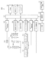
図1は本実施形態における光学機器の一例として、カメラの構成を示すブロック図である。
<First Embodiment>
FIG. 1 is a block diagram illustrating a configuration of a camera as an example of an optical apparatus according to the present embodiment.
図1において、200はカメラであり、撮像素子を有するカメラ本体と撮影レンズ100とが一体となった電子カメラを示している。101は撮影レンズ100の先端に配置された第1レンズ群で、光軸方向に進退可能に保持される。102は絞り兼用シャッタで、その開口径を調節することで撮影時の光量調節を行うほか、静止画撮影時には露光秒時調節用シャッタとしても機能する。103は第2レンズ群である。絞り兼用シャッタ102及び第2レンズ群103は一体となって光軸方向に進退し、第1レンズ群101の進退動作との連動により、変倍作用(ズーム機能)を実現する。
In FIG. 1,
105は第3レンズ群で、光軸方向の進退により、焦点調節を行う。106は光学的ローパスフィルタで、撮影画像の偽色やモアレを軽減するための光学素子である。107はCMOSセンサとその周辺回路で構成された撮像素子である。撮像素子107は、横方向m画素、縦方向n画素の受光画素のそれぞれに、後述するように、2つの光電変換素子(受光領域)が配置されている。
111はズームアクチュエータで、不図示のカム筒を回動することで、第1レンズ群101及び第2レンズ群103を光軸方向に進退駆動し、変倍操作を行う。112は絞りシャッタアクチュエータで、絞り兼用シャッタ102の開口径を制御して撮影光量を調節すると共に、静止画撮影時の露光時間制御を行う。114はフォーカスアクチュエータで、第3レンズ群105を光軸方向に進退駆動して焦点調節を行う。
115は撮影時の被写体照明用電子フラッシュで、キセノン管を用いた閃光照明装置が好適だが、連続発光するLEDを備えた照明装置を用いても良い。
121は、カメラ本体の種々の制御を司るカメラ内CPUで、演算部、ROM、RAM、A/Dコンバータ、D/Aコンバータ、通信インターフェイス回路等を有する。CPU121は、ROMに記憶された所定のプログラムに基づいて、カメラ本体が有する各種回路を駆動し、AF、撮影、画像処理と記録等の一連の動作を実行する。
本実施形態では、さらに、レンズ情報34と焦点検出位置情報35を基に切り出し角度を演算する演算回路33を有する。なお、この演算回路33としては個別のマイコンを搭載しても良いが、CPU121に内蔵してもよい。
In the present embodiment, there is further provided an
122は電子フラッシュ制御回路で、撮影動作に同期してフラッシュ115を点灯制御する。124は撮像素子駆動回路で、撮像素子107の撮像動作を制御するとともに、取得した画像信号をA/D変換してCPU121に送信する。125は画像処理回路で、撮像素子107が取得した画像のγ変換、カラー補間、JPEG圧縮等の処理を行う。
An electronic
126はフォーカス駆動回路で、焦点検出結果に基づいてフォーカスアクチュエータ114を駆動制御し、第3レンズ群105を光軸方向に進退駆動して焦点調節を行う。128は絞りシャッタ駆動回路で、絞りシャッタアクチュエータ112を駆動制御して絞り兼用シャッタ102の開口を制御する。129はズーム駆動回路で、撮影者のズーム操作に応じてズームアクチュエータ111を駆動する。
A
131はLCD等の表示器で、カメラの撮影モードに関する情報、撮影前のプレビュー画像と撮影後の確認用画像、焦点検出時の合焦状態表示画像等を表示する。132は操作スイッチ群で、電源スイッチ、レリーズ(撮影トリガ)スイッチ、ズーム操作スイッチ、撮影モード選択スイッチ等で構成される。133は着脱可能なフラッシュメモリで、撮影済み画像を記録する。
図2は本実施形態における撮像素子107の概略構成を示す回路図である。2次元CMOSエリアセンサの2列×4行分の光電変換部の範囲を示しているが、本実施形態では後述するように各画素が水平方向に2つの光電変換素子を設けているため、1列4行の4画素分の回路構成を示していることになる。
FIG. 2 is a circuit diagram showing a schematic configuration of the
図2において、1はMOSトランジスタゲートとゲート下の空乏層からなる光電変換素子の光電変換部、2はフォトゲート、3は転送スイッチMOSトランジスタ、4はリセット用MOSトランジスタである。5はソースフォロワアンプMOSトランジスタ、6は水平選択スイッチMOSトランジスタ、7はソースフォロワの負荷MOSトランジスタである。8は暗出力転送MOSトランジスタ、9は明出力転送MOSトランジスタ、10は暗出力蓄積容量CTN、11は明出力蓄積容量CTSである。12は水平転送MOSトランジスタ、13は水平出力線リセットMOSトランジスタ、14は差動出力アンプ、15は水平走査回路、16は垂直走査回路である。 In FIG. 2, 1 is a photoelectric conversion part of a photoelectric conversion element comprising a MOS transistor gate and a depletion layer under the gate, 2 is a photogate, 3 is a transfer switch MOS transistor, and 4 is a reset MOS transistor. 5 is a source follower amplifier MOS transistor, 6 is a horizontal selection switch MOS transistor, and 7 is a load MOS transistor of the source follower. 8 is a dark output transfer MOS transistor, 9 is a light output transfer MOS transistor, 10 is a dark output storage capacitor C TN , and 11 is a light output storage capacitor C TS . 12 is a horizontal transfer MOS transistor, 13 is a horizontal output line reset MOS transistor, 14 is a differential output amplifier, 15 is a horizontal scanning circuit, and 16 is a vertical scanning circuit.
図3は、Y方向の2つの光電変換素子に係る配線部の断面図を示す。同図において、17はP型ウェル、18はゲート酸化膜、19は一層目ポリシリコン、20は二層目ポリシリコン、21はn+フローティングディフュージョン(FD)部である。FD部21は2つの転送MOSトランジスタを介して2つの光電変換部と接続される。同図において、2つの転送スイッチMOSトランジスタ3のドレインとFD部21を共通化して微細化とFD部21の容量低減による感度向上を図っているが、アルミ(Al)配線でFD部21を接続しても良い。
FIG. 3 is a cross-sectional view of a wiring portion related to two photoelectric conversion elements in the Y direction. In this figure, 17 is a P-type well, 18 is a gate oxide film, 19 is a first layer polysilicon, 20 is a second layer polysilicon, and 21 is an n + floating diffusion (FD) portion. The
次に、図4のタイミングチャートを用いて、図2及び図3に示す撮像素子107における全画素独立出力の場合の動作について説明する。
Next, the operation in the case of the all-pixel independent output in the
まず、垂直走査回路16からのタイミング出力によって、制御パルスφLをハイとして垂直出力線をリセットする。また、制御パルスφR0、φPG00、φPGe0をハイとし、リセット用MOSトランジスタ4をオンとし、フォトゲート2の一層目ポリシリコン19をハイとしておく。時刻T0において、制御パルスφS0をハイとし、選択スイッチMOSトランジスタ6をオンさせ、第1及び第2ラインの画素部を選択する。次に制御パルスφR0をロウとし、FD部21のリセットを止め、FD部21をフローティング状態とし、ソースフォロワアンプMOSトランジスタ5のゲート・ソース間をスルーとする。その後、時刻T1において制御パルスφTNをハイとし、FD部21の暗電圧をソースフォロワ動作で蓄積容量CTN10に出力させる。
First, according to the timing output from the
次に、第1ラインの光電変換部1からの光電変換出力を行うため、先ず、第1ラインの制御パルスφTX00をハイとして転送スイッチMOSトランジスタ3を導通する。その後、時刻T2において制御パルスφPG00をローとして下げる。この時フォトゲート2の下に拡がっていたポテンシャル井戸を上げて、光発生キャリアをFD部21に完全転送させるような電圧関係が好ましい。従って完全転送が可能であれば制御パルスφTXはパルスではなくある固定電位でもかまわない。
Next, in order to perform photoelectric conversion output from the
時刻T2でフォトダイオードの第1ラインの光電変換部1からの電荷がFD部21に転送されることにより、FD部21の電位が光に応じて変化することになる。この時ソースフォロワアンプMOSトランジスタ5がフローティング状態であるので、FD部21の電位を時刻T3において制御パルスφTsをハイとして蓄積容量CTS11に出力する。この時点で第1ラインの画素の暗出力と明出力はそれぞれ蓄積容量CTN10とCTS11に蓄積される。時刻T4で制御パルスφHCを一時ハイとして水平出力線リセットMOSトランジスタ13を導通して水平出力線をリセットし、水平転送期間において水平走査回路15の走査タイミング信号により水平出力線に画素の暗出力と明出力を出力させる。この時、蓄積容量CTN10とCTS11の差動増幅器14によって、差動出力VOUTを取れば、画素のランダムノイズ、固定パターンノイズを除去したS/Nの良い信号が得られる。
At time T 2 , the electric charge from the
また、第1ラインの光電変換部1の暗出力及び明出力は、同時に夫々の垂直出力線に接続された蓄積容量CTN10とCTS11に蓄積されている。従って、水平転送MOSトランジスタ12を順次オンとしていくことにより、夫々の蓄積容量CTN10とCTS11に蓄積された電荷は、水平出力線に順次読み出され、差動増幅器14から出力される。
Further, the dark output and the bright output of the
また、本実施形態では、差動出力VOUTをチップ内で行う構成を示している。しかしながら、チップ内に含めず、外部で従来のCDS(Correlated Double Sampling:相関二重サンプリング)回路を用いても同様の効果が得られる。 In the present embodiment, a configuration in which the differential output V OUT is performed in the chip is shown. However, the same effect can be obtained even if a conventional CDS (Correlated Double Sampling) circuit is used outside without being included in the chip.
一方、第1ラインの光電変換部1から蓄積容量CTS11に明出力を出力した後、制御パルスφR0をハイとしてリセット用MOSトランジスタ4を導通し、FD部21を電源VDDにリセットする。第1ラインの電荷の水平転送が終了した後、第2ラインの光電変換部1からの読み出しを行う。第2ラインの読み出しは、上述した第1ラインと同様にまず制御パルスφTXe0、制御パルスφPGe0を駆動させる。次に、制御パルスφTN、φTSに夫々ハイパルスを供給して、蓄積容量CTN10とCTS11に夫々暗出力と明出力を蓄積し、暗出力及び明出力を取り出す。
On the other hand, after outputting a bright output from the
以上の駆動により、第1、第2ラインの読み出しを夫々独立に行うことができる。この後、垂直走査回路16を走査させ、同様にして第2n+1、第2n+2(n=1,2,…)の読み出しを行えば、全光電変換部1からの独立出力が行える。即ち、n=1の場合は、まず制御パルスφS1をハイとし、次にφR1をローとし、続いて制御パルスφTN、φTX01をハイとする。そして、制御パルスφPG01をロー、制御パルスφTSをハイ、制御パルスφHCを一時ハイとして第3ラインの各光電変換部1から暗出力及び明出力を読み出す。続いて、制御パルスφTXe1、φPGe1及び上記と同様に制御パルスを印加して、第4ラインの各光電変換部1から暗出力及び明出力を読み出す。
With the above driving, the first and second lines can be read independently. Thereafter, by scanning the
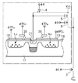
次に、本実施形態における位相差検出方法について説明する。図5は、瞳分割機能を有する撮像素子107の画素の構成を示す図である。図5(a)は不図示の撮像光学系の光軸上にある中央像高画素、図5(b)は水平に像高を持った周辺像高画素の構成を示す図である。60は光電変換素子であり、1画素につき2つの光電変換素子60a、60bを配置することにより、瞳分割機能を持たせている。
Next, the phase difference detection method in this embodiment will be described. FIG. 5 is a diagram illustrating a configuration of pixels of the
61はオンチップマイクロレンズであり、光電変換素子60に効率良く光を集める。オンチップマイクロレンズ61は、図5(a)では光電変換素子60a、60bの境界に光軸が合っており、図5(b)では光電変換素子60a、60bの境界に対し光軸をずらして配置されている。62は平坦化膜、63はカラーフィルタ、64は配線、65は層間絶縁膜である。2つの光電変換素子60a、60bは、図2の各行における2つの光電変換部1に対応している。また、焦点検出動作を行う場合は、2つの光電変換素子60a、60bからの出力を個別の信号として扱うが、一般撮影を行う場合は、2つの光電変換素子60a、60bの出力の加算信号を、1画素の画素信号として取り扱う。
次に、本実施形態において、1対の位相差検出用信号を撮像素子107で検出する動作について説明する。
Next, an operation for detecting a pair of phase difference detection signals by the
図6は、撮像素子107上の焦点検出領域を説明する図であり、撮像素子107をその受光面の撮影レンズ100側から見た状態を示す。図6(a)は、撮像素子107上の対角位置にある位相差検出用信号の演算処理領域(以下、「焦点検出領域」と呼ぶ。)31の形状を示している。また、図6(b)は、焦点検出領域31を拡大して示している。
FIG. 6 is a diagram for explaining a focus detection area on the
32−1、32−2、…、32−n−1、32−nは、それぞれ焦点検出用画素ブロックであり、それぞれ、複数配列された画素から構成されている。図6(c)は、焦点検出用画素ブロック32ー1の構成を示しているが、他の焦点検出用画素ブロックも同様の構成を有している。 32-1, 32-2,..., 32-n-1, 32-n are focus detection pixel blocks, each of which includes a plurality of pixels. FIG. 6C shows the configuration of the focus detection pixel block 32-1, but the other focus detection pixel blocks have the same configuration.
図6(c)に示すように、焦点検出用画素ブロック32−1に含まれる各画素には、通常の撮影を行うためにベイヤー配列のカラーフィルタが配置されている。そして同一画素において、同一色のカラーフィルタが配置された2つの光電変換素子(GaとGb、RaとRb、BaとBb)の出力を加算することにより、通常撮影時に画像信号を入手することが可能となる。 As shown in FIG. 6C, each pixel included in the focus detection pixel block 32-1 is provided with a Bayer color filter in order to perform normal photographing. Then, in the same pixel, by adding the outputs of two photoelectric conversion elements (Ga and Gb, Ra and Rb, Ba and Bb) in which color filters of the same color are arranged, an image signal can be obtained during normal shooting. It becomes possible.
一方、焦点検出処理を行う場合は、画素ブロック32−1内の、光電変換素子60aに対応する光電変換素子32−1aからの出力をすべて積算することにより、画素ブロック32−1の焦点検出用画素のA像信号とする。また、画素ブロック32−1内の、光電変換素子60bに対応する光電変換素子32−1bからの出力をすべて積算することにより、画素ブロック32−1の焦点検出用画素のB像信号とする。このように、光電変換素子32−1a、32−1bそれぞれからの出力の積算信号をA像信号、B像信号とすることにより、低輝度における画素信号のS/Nに効果を持たせることができる。
On the other hand, when the focus detection process is performed, the outputs from the photoelectric conversion elements 32-1a corresponding to the
そして、図6(b)における焦点検出用画素ブロック32−1、32−2、…、32−n−1、32−nそれぞれのA像信号、B像信号によって、一対の位相差検出用信号を生成することができる。 Then, a pair of phase difference detection signals is obtained by the A image signal and the B image signal of the focus detection pixel blocks 32-1, 32-2,..., 32-n-1, 32-n in FIG. Can be generated.
ここではA像信号、B像信号として、画素ブロック内の信号を加算したものを示したが、焦点検出用画素は画素ブロック内で信号加算しないように構成してもよい。 Here, the A image signal and the B image signal are obtained by adding signals in the pixel block, but the focus detection pixels may be configured not to add signals in the pixel block.
本実施形態における焦点検出領域31は、上述した口径食によって生じる、A像、B像瞳領域の重心位置78a、78bの傾き角度θに合わせている。焦点検出領域31の角度θは、画素ブロック32ー1〜nの縦方向の段差を撮像素子107の単位画素の整数倍にしなければならないため、横方向には平行ブロックが複数個ずつ束ねた形で切り出し角度をつけるようにしている。
In the present embodiment, the
図7は瞳分割機能を有する画素の受光感度を示す図であり、横軸が入射角度、縦軸が受光感度である。図7(a)は中央像高画素の2つの光電変換素子60a、60bそれぞれの受光感度(図ではそれぞれA像感度、B像感度と称している。)を表す。また、図7(b)は周辺像高画素の光電変換素子60a、60bそれぞれの受光感度を表す。図7からわかるように、中央像高画素では2つの光電変換素子60a、60bの感度は入射角0度に対して対称な特性になっている。一方、周辺像高画素では2つの光電変換素子60a、60bの感度は入射角約−2度に対して対称な特性になっている。
FIG. 7 is a diagram showing the light receiving sensitivity of a pixel having a pupil division function, in which the horizontal axis represents the incident angle and the vertical axis represents the light receiving sensitivity. FIG. 7A shows the light receiving sensitivity (referred to as A image sensitivity and B image sensitivity, respectively) of the two
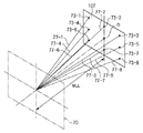
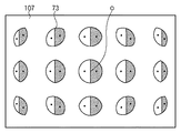
図8は、撮像素子の各像高での画素の受光感度中心を説明する図である。像高とは、撮像画角に対する前記焦点状態検出位置の位置情報を表す。図8において、107は撮像素子であり、70はマイクロレンズ(ML)瞳領域である。Oは、撮像素子107における不図示の撮像光学系の光軸との交点であり、73−1〜8は各像高の画素位置を示す。
FIG. 8 is a diagram illustrating the light receiving sensitivity center of a pixel at each image height of the image sensor. The image height represents position information of the focus state detection position with respect to the imaging field angle. In FIG. 8, 107 is an image sensor, and 70 is a microlens (ML) pupil region. O is an intersection with an optical axis of an imaging optical system (not shown) in the
中央像高画素Oでは、光電変換素子60a、60bを1つの受光領域と見なした場合、光電変換素子60の受光領域中心とオンチップマイクロレンズ61の光軸とが一致している。そして像高が高くなるにつれオンチップマイクロレンズ61の光軸を徐々にずらして、像高によらずに画素の光電変換素子60の受光領域中心が所定の光学系光軸上の一点に向かうようにしている。ここで、撮像素子107から受光領域中心が向かっている点までの距離をオンチップマイクロレンズ瞳距離MLLと呼ぶ。また、光軸を垂線とするオンチップマイクロレンズ瞳距離上の面をML瞳領域70と称する。77−1〜8は、各像高での受光感度中心の角度ズレを示したものである。図からわかるように、感度中心の角度ズレは像高に依らずに瞳距離MLLの光軸上に向かっている。
In the central image height pixel O, when the
図9は口径食の形状を説明する図であり、図9(a)は斜視図、図9(b)及び(c)は投影図である。図9(a)で示すようにX軸、Y軸、Z軸を定義した場合、図9(b)は図9(a)のZ(+)方向から見たML瞳領域を示しており、図9(c)は図9(a)のY(−)方向から描いたものである。撮影レンズは一般に複数枚のレンズで構成されており、撮影レンズの光軸と撮像素子107の交点以外に位置する周辺の画素73は、主に2つの射出窓によって光束が制限される。1つは、複数枚あるレンズ枠のうち、絞り位置から被写体に近い側のレンズ保持枠の中で絞り位置での投影半径が最も小さいレンズ枠である。もう1つは、絞り位置から撮像素子107に近い側のレンズ保持枠の中で、絞り位置での投影半径が最も小さいレンズ枠である。これらの2つのレンズ枠によって光束が制限される。ここで、被写体に近い側のレンズ保持枠を撮影レンズの第1の射出窓71とし、撮像素子107に近い側のレンズ保持枠を撮影レンズの第2の射出窓72とする。
FIG. 9 is a diagram for explaining the shape of vignetting. FIG. 9A is a perspective view, and FIGS. 9B and 9C are projection views. When the X axis, Y axis, and Z axis are defined as shown in FIG. 9A, FIG. 9B shows the ML pupil region viewed from the Z (+) direction of FIG. 9A, FIG. 9C is drawn from the Y (−) direction of FIG. The photographic lens is generally composed of a plurality of lenses, and the luminous flux of the
投影射出窓71−1は、第1の射出窓71を周辺画素73からML瞳領域70に投影したものである。投影射出窓72−1は、第2の射出窓72を周辺画素73からML瞳領域70に投影したものである。周辺画素73は、投影射出窓71−1と投影射出窓72−1によって切り出される焦点検出開口瞳76を通過した光束を受光する。周辺画素73は、図5(b)に示したように2つの光電変換素子60a、60bから構成されている。そして、撮影レンズ側に形成されたオンチップマイクロレンズ61によって、2つの光電変換素子60a、60bは、撮影レンズの瞳の異なる位置を透過した光束をそれぞれ受光するように構成されている。
The projection exit window 71-1 is obtained by projecting the
周辺画素73のオンチップマイクロレンズ61は、ML瞳領域の光軸に向かうように偏心されている。そのため、図9(b)に示すように、光電変換素子60aが受光する光束の領域74a(以下、A像瞳領域74aと呼ぶ。)と光電変換素子60bが受光する光束の領域74b(以下、B像瞳領域74bと呼ぶ。)との境界線は、撮影レンズの光軸を通過する。図9(b)において、78aはA像瞳領域74aの重心位置、78bはB像瞳領域74bの重心位置を表している。
The on-
図9(c)において、L71は撮像素子107から第1の射出窓71までの距離、L72は撮像素子107から第2の射出窓72までの距離である。D71は第1の射出窓71の直径、D72は第2の射出窓72の直径である。A像瞳領域74aとB像瞳領域74bは、図9(b)からも分かるように、境界線に対して線対称な形状とはならず、重心位置78a、78bの位置も水平とはならない。
In FIG. 9C, L71 is the distance from the
周辺画素73では、光電変換素子60aが受光する光束の領域は図9(b)のA像瞳領域74aとして示したものとなる。また、光電変換素子60bが受光する光束の領域は図9(b)のB像瞳領域74bとして示したものとなる。更に、2つの光電変換素子60a、60bの瞳領域の重心位置は、図9(b)の重心位置78a、78bで示したものになる。
In the
ここで重心位置78aの座標を(xa、ya)、重心位置78bの座標を(b、yb)とすると、傾き角度θは、
tanθ={(ya−yb)/(xa−xb)} …(1)
Here, if the coordinates of the center of
tan θ = {(ya−yb) / (xa−xb)} (1)
の関係式より求められる。
一方、A像、B像瞳領域の重心位置78a、78bの座標は、撮像素子107上の画素73を像高として表した座標(xs、ys)と、第1及び第2の射出窓71、72の情報と、撮像素子107固有のML瞳距離MLLとから、幾何学的に求めることができる。ここで第1及び第2の射出窓71、72の情報とは、以下の情報を示す。即ち、図9(c)における、撮像素子107から第1の射出窓71までの距離L71と、撮像素子107から第2の射出窓72までの距離L72と、第1の射出窓71の直径D71と、第2の射出窓72の直径D72である。
It is obtained from the relational expression.
On the other hand, the coordinates of the
撮影レンズ100の種類が変わったり、ズーム比、F値が変わったりすると、上記射出窓の情報は異なってくる。そのため、撮影レンズ100の種類や、ズーム比、F値に対応する射出窓情報を予め光学計算にて算出しておき、撮影レンズ100の各条件での射出窓情報(レンズ情報34)をレンズ内のメモリに格納しておき、必要に応じて射出窓情報を受け渡すようにする。
When the type of the taking
図10は、撮像素子107上の像高毎の口径食の形状を示したもので、網掛けした部分がA像の感度領域、白部分がB像の感度領域を表している。また黒点はそれぞれの重心位置を示している。
FIG. 10 shows the shape of vignetting for each image height on the
図10から分かるように、画面中央(撮影レンズの光軸上)及び、画面中央に対して、水平方向及び垂直方向では、A像瞳領域とB像瞳領域の重心は水平状態を保っているが、画面中央に対して対角方向においてはA像瞳領域とB像瞳領域の重心が傾いてくる。この重心の傾きは像のピントがずれたときの像ズレ方向の傾きと一致する。 As can be seen from FIG. 10, the centroids of the A image pupil region and the B image pupil region remain horizontal in the horizontal direction and the vertical direction with respect to the screen center (on the optical axis of the photographing lens) and the screen center. However, the center of gravity of the A image pupil region and the B image pupil region is inclined in the diagonal direction with respect to the center of the screen. The inclination of the center of gravity coincides with the inclination in the image shift direction when the image is out of focus.
図11は、撮像素子107の対角位置での像ズレ方向が斜めとなる場合の、被写体像の傾きと位相差信号のズレ量を説明する図である。ここでは、撮影像を正立像として見せるために撮像素子107の裏面(Z軸(−)方向)からの像を180度回転させてある。
FIG. 11 is a diagram illustrating the tilt of the subject image and the amount of shift of the phase difference signal when the image shift direction at the diagonal position of the
図11(a)は対角焦点検出位置での位相差信号の演算処理領域80を示しており、被写体像として同一測距面上で、左斜めに倒れた像1、垂直像2、右斜めに倒れた像3を想定している。また、焦点検出を行う演算処理領域80から得られる光電変換素子60aの画素列から得られる信号をA像信号、光電変換素子60bの画素列から得られる信号をB像信号としている。この場合、図11(b)は前ピンで演算処理領域80に結像したA像及びB像の様子、図11(c)は前ピンで画素列から得られる信号である、いわゆる位相差信号(A像信号、B像信号)及びそのズレ量を示している。また、図11(d)は後ピンで演算処理領域80に結像したA像及びB像の様子、図11(e)は後ピンで画素列から得られる位相差信号(A像信号、B像信号)及びそのズレ量を示している。また、被写体像として像1、像2、像3に対応するそれぞれのA像をa1、a2、a3、それぞれのB像をb1、b2、b3としている。
FIG. 11A shows the phase difference signal
図11(c)から分かるように、前ピンで被写体像が垂直の場合は、ピントズレによる像ズレの水平成分と演算処理領域80での位相差ズレ量S2とは一致する。これに対し、被写体像が斜めの場合は、ピントズレによる像ズレの水平成分と演算処理領域80での位相差ズレ量(S1、S3)との間に食い違いが生じる。例えば、左斜めに倒れた像1では、ピントズレによる像ズレの水平成分S2よりも演算処理領域80での位相差ズレ量S1が小さくなり、また右斜めに倒れた像3では、逆に演算処理領域80での位相差ズレ量S3が大きくなる。
As can be seen from FIG. 11C, when the subject image is vertical at the front pin, the horizontal component of the image shift due to the focus shift matches the phase difference shift amount S <b> 2 in the
同様に、図11(e)に示すように、後ピンでの被写体像が垂直の場合はピントズレによる像ズレの水平成分と演算処理領域80での位相差ズレ量S2’とは一致する。これに対し、被写体像が斜めの場合は、ピントズレによる像ズレの水平成分と演算処理領域80での位相差ズレ量(S1’、S3’)との間に食い違いが生じる。
Similarly, as shown in FIG. 11E, when the subject image at the rear pin is vertical, the horizontal component of the image shift due to the focus shift matches the phase difference shift amount S2 'in the
図12は、本実施形態における、被写体像の傾きと位相差信号のズレ量を説明する図である。ここでは、撮影像を正立像として見せるために撮像素子107の裏面からの像を180度回転させてある。
FIG. 12 is a diagram for explaining the inclination of the subject image and the amount of deviation of the phase difference signal in the present embodiment. Here, the image from the back surface of the
図12(a)は対角焦点検出位置での位相差信号の焦点検出領域31を示しており、被写体像として同一測距面上で、左斜めに倒れた像1、垂直像2、右斜めに倒れた像3を想定している。図12(b)は前ピンで焦点検出領域31に結像したA像及びB像の様子、図12(c)は前ピンで各焦点検出用画素ブロックから得られるA像信号及びB像信号のズレ量を示している。また、図12(d)は後ピンで焦点検出領域31に結像したA像及びB像の様子、図12(e)は後ピンで各焦点検出用画素ブロックから得られるA像信号及びB像信号のズレ量を示している。また、被写体像として像1、像2、像3に対応するそれぞれのA像をa1、a2、a3、それぞれのB像をb1、b2、b3としている。
FIG. 12A shows the
図12(c)からわかるように、前ピンでは被写体像傾きに依らず、ピントズレによる像ズレの水平成分と焦点検出領域31での位相差ズレ量(S1、S2、S3)は全て一致する。
As can be seen from FIG. 12C, the horizontal component of the image shift due to the focus shift and the phase difference shift amount (S1, S2, S3) in the
同様に、図12(e)からわかるように、後ピンにおいても被写体像傾きに依らず、ピントズレによる像ズレの水平成分と焦点検出領域31での位相差ズレ量(S1’、S2’、S3’)は全て一致する。
Similarly, as can be seen from FIG. 12 (e), the horizontal component of the image shift due to the focus shift and the phase difference shift amount (S1 ′, S2 ′, S3) in the
このように、像ズレ方向の角度に焦点検出領域31の角度を一致させることにより、焦点状態の検出精度の向上を図ることが可能となる。
Thus, by making the angle of the
以下、図13の画像を例にして、図14のフローチャートを参照しながら、本実施形態における焦点ずれ量(デフォーカス量)検出動作について説明する。 Hereinafter, the operation of detecting the defocus amount (defocus amount) in the present embodiment will be described with reference to the flowchart of FIG. 14 using the image of FIG. 13 as an example.
図13では、撮影像を正立像として見せるために撮像素子107の裏面からの像を180度回転させてある。図13(a)において、40−1〜4は焦点状態の検出位置候補であり、図13(b)では各検出位置候補での焦点検出領域41−1〜4を表している。
In FIG. 13, the image from the back surface of the
本実施形態では、選択された焦点状態検出位置に対応する焦点検出領域を設定し、当該焦点検出領域に対応する2像の位相差に基づいて当該焦点検出領域における焦点ずれ量を検出する。ここでは、図13(a)において、複数の焦点状態の検出位置候補の中から、撮影者によって画面中心から外れたエリア(周辺エリア)が選択された場合について説明する。 In the present embodiment, a focus detection region corresponding to the selected focus state detection position is set, and a defocus amount in the focus detection region is detected based on the phase difference between the two images corresponding to the focus detection region. Here, a case where an area (peripheral area) deviated from the center of the screen by the photographer is selected from a plurality of focus position detection position candidates in FIG. 13A will be described.
まず画像情報、例えば像のコントラスト信号などによって、被写体像から検出位置候補を自動検出し、表示する(ステップS1)。次に、検出位置候補のいずれか1つ(図13(a)ではselectで示されている検出位置候補40−1)の選択を受けて(ステップS2)、レンズ情報34(射出窓情報)を取得する(ステップS3)。このとき、レンズ情報34として、CPU121にてレンズ内のメモリにアクセスすることで、現時点の撮影レンズ100の射出窓情報を取得する。A像、B像瞳領域の重心位置は、前述したように、焦点検出位置情報35とレンズ情報34(射出窓情報)、撮像素子107固有のML瞳距離MLLを元に算出することが可能である。そして、演算回路33により、A像及びB像の重心を算出し、上述した式(1)で示した像ずれ方向、つまり、焦点検出領域31の傾き(ここではθ1)を取得する(ステップS4)。
First, detection position candidates are automatically detected from a subject image based on image information, for example, an image contrast signal, and displayed (step S1). Next, in response to the selection of any one of the detection position candidates (detection position candidate 40-1 indicated by select in FIG. 13A) (step S2), lens information 34 (exit window information) is obtained. Obtain (step S3). At this time, as the
例えば単焦点レンズのようにレンズ情報がほとんど変化しないカメラシステムにおいては、焦点検出位置情報に対応して切り出し角度のみを変えればよい。また、焦点検出位置の変更をしない仕様(焦点検出位置が変動しない仕様)であれば(例えば顔検出機能により焦点検出位置が変化するような仕様を採用しなければ)、レンズ情報に対応して切り出し角度のみを変えればよい。 For example, in a camera system in which lens information hardly changes like a single focus lens, only the cut-out angle needs to be changed corresponding to the focus detection position information. If the specification does not change the focus detection position (specification that the focus detection position does not change) (for example, unless a specification that changes the focus detection position by the face detection function is adopted), the lens information corresponds to the lens information. Only the cutting angle needs to be changed.
次に、演算回路33により得られた像ずれ方向(傾きθ1)に基づいて、CPU121により焦点検出領域(ここでは、図13(b)の41−1)の形状(切り出し領域)を算出する(ステップS5)。
Next, based on the image shift direction (inclination θ1) obtained by the
そして、ステップS5で設定された焦点検出領域の焦点検出用画素から信号を選択的に読み出し(ステップS6)、A像信号とB像信号から得られた対の位相差検出用信号を基に、CPU121により自己相関処理を行う(ステップS7)。以上の処理により、撮影光学系の焦点ずれ量(デフォーカス量)を検出する(ステップS8)ことが可能となる。ここでステップS7における自己相関処理とは、対の位相差検出用信号の位相差ズレを精度良く計算する手法であり、位相差検出方式の焦点検出演算として一般的に用いられる方式である。そのため、その手法についての詳細説明はここでは省略する。
Then, a signal is selectively read from the focus detection pixels in the focus detection area set in step S5 (step S6), and based on the pair of phase difference detection signals obtained from the A image signal and the B image signal, The
以上の処理により、画面周辺部においても、像ズレ方向に合った焦点検出領域を選択することが可能となる。 With the above processing, it is possible to select a focus detection region that matches the image shift direction even in the peripheral portion of the screen.
なお、ここでは焦点検出領域31を角度を付けて切り出す方法として、焦点検出領域31内の画素信号を選択的に読み出す方法を記載したが、全画素読み出し後、焦点検出領域31の画素信号のみを演算処理する方法をとることもできる。
Here, as a method of cutting out the
また、上記処理において、例えば撮影レンズ100のズーム比を変えると、同一の焦点検出位置でも口径食による像ズレ方向が変化する。その場合においても上述のフローを繰り返し行うことにより、適宜レンズ情報を取得して最適な切り出し角度に設定可能となるため、検出誤差を抑えることができる。
In the above processing, for example, when the zoom ratio of the photographing
CPU121は、検出した焦点ずれ量(デフォーカス量)に基づいて、撮影レンズ100に含まれる第3レンズ群105のフォーカスレンズの合焦位置を算出する。そして、フォーカス駆動回路126及びフォーカスアクチュエータ114を介して、第3レンズ群105を駆動することにより、全ズーム領域における自動焦点調節(AF)を行うことが可能となる。
The
上記の通り、本実施形態によれば、焦点調節領域を、レンズ情報(ズーム比やF値)及び焦点調節領域の像高に応じて、撮像光学系の口径食に対応するように、画素配列方向から角度をつけて切り出す。これにより、口径食によって焦点検出性能を低下させる斜め被写体像においても検出誤差を抑えることができる。 As described above, according to the present embodiment, the pixel adjustment is performed so that the focus adjustment area corresponds to the vignetting of the imaging optical system according to the lens information (zoom ratio and F value) and the image height of the focus adjustment area. Cut out at an angle from the direction. Thereby, it is possible to suppress a detection error even in an oblique subject image whose focus detection performance is deteriorated by vignetting.
<第2の実施形態>
次に、本発明の第2の実施形態について説明する。なお、カメラの全体構成は第1の実施形態で説明したものと同様であるため、ここでは説明を省略する。
上述した第1の実施形態では、撮影する画像に応じて、任意の領域を焦点調節領域として設定することを可能としたが、本実施形態では、焦点検出領域が固定されているところが第1の実施形態と異なる。
<Second Embodiment>
Next, a second embodiment of the present invention will be described. Since the entire configuration of the camera is the same as that described in the first embodiment, the description thereof is omitted here.
In the first embodiment described above, an arbitrary area can be set as the focus adjustment area in accordance with the image to be captured. In the present embodiment, the focus detection area is fixed. Different from the embodiment.
図15は本発明の第2の実施形態における焦点検出領域を示す図である。 FIG. 15 is a diagram showing a focus detection area in the second embodiment of the present invention.
図15(a)において50−1〜50−15は、固定された15点の焦点検出枠を示し、図15(b)において51−1〜51−15は固定された15点の焦点検出領域を示す。 In FIG. 15A, reference numerals 50-1 to 50-15 denote fixed 15-point focus detection frames, and in FIG. 15B, reference numerals 51-1 to 51-15 denote fixed 15-point focus detection areas. Indicates.
本実施形態では、単焦点レンズまたは、レンズのズーム比が変わっても口径食の形状があまり変化しない場合を想定したものとなる。この場合、像高毎の像ズレ方向は予め決まった角度となるために、撮像素子の切り出し領域を変える必要が無くなる。 In the present embodiment, it is assumed that the shape of the vignetting does not change much even if the zoom ratio of the single focus lens or the lens changes. In this case, since the image shift direction for each image height is a predetermined angle, it is not necessary to change the cutout region of the image sensor.
以下、図15の画像を例にして、図16のフローチャートを参照しながら、本実施形態における焦点ずれ量(デフォーカス量)の検出動作について説明する。 Hereinafter, the detection operation of the defocus amount (defocus amount) in the present embodiment will be described with reference to the flowchart of FIG. 16 using the image of FIG. 15 as an example.
不図示のシャッタボタンが半押しされると、15点の焦点検出枠50−1〜50−15に対応する焦点検出領域51−1〜51−15の焦点検出用画素から信号を読み出す(ステップS11)。得られた対の位相差信号(A像信号とB像信号)の一致度やコントラストを評価し(ステップS12)、最も焦点検出位置候補としてふさわしい焦点検出領域を自動選択する(ステップS13)。なお、焦点検出領域の選択の仕方としては、例えば、顔や、カメラ200に最も近い被写体などを含む焦点検出領域を選択することが考えられるが、任意の条件に基づいて選択するように制御すればよい。そして、A像信号とB像信号から得られた対の位相差検出用信号を基に、CPU121により自己相関処理を行って(ステップS14)、撮影光学系の焦点ずれ量(デフォーカス量)を検出する(ステップS15)。
When a shutter button (not shown) is half-pressed, a signal is read from the focus detection pixels in the focus detection areas 51-1 to 51-15 corresponding to the 15 focus detection frames 50-1 to 50-15 (step S11). ). The degree of coincidence and contrast of the obtained pair of phase difference signals (A image signal and B image signal) are evaluated (step S12), and a focus detection region most suitable as a focus detection position candidate is automatically selected (step S13). As a method for selecting the focus detection area, for example, a focus detection area including a face or a subject closest to the
上記の通り、本実施形態によれば、焦点検出領域の像高に対して最適な切り出し角度の焦点検出領域を切り出すことができるため、口径食によって焦点検出性能を低下させる斜め被写体像においても検出誤差を抑えることができる。 As described above, according to the present embodiment, since the focus detection area having the optimum cut-out angle with respect to the image height of the focus detection area can be cut out, detection can be performed even in an oblique subject image whose focus detection performance is degraded by vignetting. Errors can be suppressed.
なお、上述した第1及び第2の実施形態では、撮像素子107の一部の画素の受光部を2分割することで瞳分割機能を付与させた場合について説明した。しかしながら、本発明はこれに限るものではなく、特許文献1で示したように、オンチップマイクロレンズの光軸に対して受光部の感度領域を偏心させることで瞳分割機能を付与させたものに対しても同様の効果を得ることができる。また特許文献1で示されたように標準画素の一部に瞳の異なる焦点検出用画素を部分的に配置して、離散的な瞳分離画像を元に焦点検出を行う構造のものに対しても同様の効果を得ることができる。
In the first and second embodiments described above, the case where the pupil division function is provided by dividing the light receiving unit of some pixels of the
図17は、瞳分割機能を有する撮像素子の画素の構成を示す図である。61はオンチップマイクロレンズであり、光電変換素子60に効率良く光を集める。62は平坦化膜、63はカラーフィルタ、64は配線、65は層間絶縁膜である。
FIG. 17 is a diagram illustrating a pixel configuration of an image sensor having a pupil division function.
図17(a)は受光感度が右方向に感度ピークを持つ焦点検出画素(左側の画素)と標準画素(右側の画素)を示した図である。また図17(b)は標準画素(右側の画素)と受光感度が左方向に感度ピークを持つ焦点検出画素(左側の画素)を示した図である。図17(a)では、最下部の配線層64aの開口を左側にシフトすることにより、右方向に感度ピーク瞳分割機能を持たせている。図17(b)では、最下部の配線層64bの開口を右側にシフトすることにより、左方向に感度ピーク瞳分割機能を持たせている。また焦点検出画素部のカラーフィルタ63Wは、光量拡大を図るために、透明層となっている。
FIG. 17A is a diagram showing a focus detection pixel (left pixel) and a standard pixel (right pixel) whose light reception sensitivity has a sensitivity peak in the right direction. FIG. 17B is a diagram showing a standard pixel (right pixel) and a focus detection pixel (left pixel) having a sensitivity peak in the left direction of light receiving sensitivity. In FIG. 17A, the sensitivity peak pupil division function is provided in the right direction by shifting the opening of the
図18は、撮像素子107上の焦点検出領域を説明する図であり、撮像素子107をその受光面の撮影レンズ100側から見た状態を示す。図18(a)は、撮像素子107上の対角位置にある焦点検出領域31の形状を示している。
FIG. 18 is a diagram for explaining a focus detection area on the
また、図18(b)は焦点検出領域31を拡大して示している。32−1、32−2、…、32−n−1、32−nは、それぞれ焦点検出用画素ブロックであり、それぞれ、複数配列された画素から構成されている。
FIG. 18B shows the
図18(c)は、図18(b)の撮像素子107上の一部分107−1を拡大した、撮像素子107に配置されている画素のパターン構成を示す図である。図18(c)に示すように、1対の焦点検出用画素a、bは、ブロック8x8画素を基本パターンとして離散配置されており、標準画素部にはベイヤー配列のカラーフィルタが配置されている。画素ブロック32−1内には、焦点検出画素が縦に8対あり、焦点検出a、焦点検出bそれぞれの出力を加算することにより、画素ブロック32−1の焦点検出用画素のA像信号、B像信号とする。このように、光電変換素子32−1内の焦点検出画素8画素分の出力の積算信号をA像信号、B像信号とすることにより、低輝度における画素信号のS/Nに効果を持たせることができる。
FIG. 18C is a diagram illustrating a pattern configuration of pixels arranged in the
そして、図18(b)における焦点検出用画素ブロック32−1、32−2、…、32−n−1、32−nそれぞれのA像信号、B像信号によって、一対の位相差検出用信号を生成することができる。 Then, a pair of phase difference detection signals is obtained by the A image signal and the B image signal of the focus detection pixel blocks 32-1, 32-2,..., 32-n-1, 32-n in FIG. Can be generated.
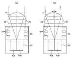
以上、撮像素子上に構成される焦点検出画素における本実施形態の適用方法を説明したが、さらに、従来より一眼レフカメラで使用されている2次結像光学系を用いた焦点検出装置に適用しても良い(図19)。この場合、焦点検出用センサは撮像素子と同様に正方画素が複数配列された構成を取っており、切り出し形状を任意に選択することが可能となっている。図20(a)は、2次結像面(107−2)上で定義される瞳形状がレンズのビネッティング(口径食)により変形している様子を示している。この場合に、重心傾きθに合わせて検出画素切り出し形状を設定することを示したのが図20(b)、(c)である。このような構成によって本発明における効果が期待できる。 As described above, the application method of the present embodiment in the focus detection pixel configured on the image sensor has been described. Further, the application method is applied to a focus detection apparatus using a secondary imaging optical system that has been conventionally used in a single-lens reflex camera. You may do it (FIG. 19). In this case, the focus detection sensor has a configuration in which a plurality of square pixels are arranged in the same manner as the image sensor, and the cutout shape can be arbitrarily selected. FIG. 20A shows a state in which the pupil shape defined on the secondary imaging plane (107-2) is deformed by lens vignetting. In this case, FIGS. 20B and 20C show that the detection pixel cutout shape is set in accordance with the gravity center inclination θ. With such a configuration, the effect of the present invention can be expected.
Claims (9)
撮影レンズの異なる瞳領域を透過した対の光束をそれぞれ受光する複数の焦点検出用画素を有し、当該複数の焦点検出用画素から対の像の信号が出力される撮像素子と、
撮像画角に対する前記検出領域の位置情報と、前記撮影レンズの射出窓情報とに応じて、前記検出領域の傾きを決定する決定手段と、
前記複数の焦点検出用画素のうち、前記決定手段により傾きの決定された前記検出領域に対応する焦点検出用画素から得られる前記対の像の信号の位相差に基づいて、焦点ずれ量を検出する検出手段と
を有することを特徴とする焦点検出装置。 Based on the phase difference between the two images corresponding to the detection area A focus detecting device for detecting the defocus amount in the detection area,
An image sensor that has a plurality of focus detection pixels that respectively receive a pair of light fluxes that have passed through different pupil regions of the photographic lens, and that outputs a pair of image signals from the plurality of focus detection pixels;
Determining means for determining an inclination of the detection area according to position information of the detection area with respect to an imaging angle of view and exit window information of the photographing lens;
Among the plurality of focus detection pixels, based on the phase difference of the signals of the pair of images obtained from the focus detection pixels corresponding to the detection area determined slope by said determining means, detecting a defocus amount And a focus detection device.
予め設定された複数の検出領域から1つを選択する選択手段と、
前記選択された検出領域に対応する焦点検出用画素から得られる前記対の像の信号の位相差に基づいて、焦点ずれ量を検出する検出手段と、を有し、
前記複数の検出領域は、各検出領域の像高に応じて異なる傾きを有することを特徴とする焦点検出装置。 An imaging element having a plurality of focus detection pixels, the signal of the image of the pair from the plurality of focus detection pixels are output for receiving the light beam pair transmitted through different pupil areas of shadow lens respectively shooting,
Selection means for selecting one from the area out a plurality of detection set in advance,
On the basis of the phase difference of the selected detection region signal of the pair of images obtained from the focus detection pixels corresponding includes a detecting means for detecting a focus Tenzure amount, a,
Wherein the plurality of detection areas, focus detection apparatus characterized by having a different inclination depending on the image height of each detection region.
撮影レンズの異なる瞳領域を透過した対の光束をそれぞれ受光して、対の像の信号を出力する焦点検出用画素を含む撮像素子と、
前記対の光束による対の像の像ズレ方向に対応して、前記検出領域の傾きを決定する決定手段と、
前記決定手段により傾きの決定された前記検出領域に対応する焦点検出用画素から得られる前記対の像の信号の位相差に基づいて、焦点ずれ量を検出する検出手段と
を有することを特徴とする焦点検出装置。 A focus detection device that detects a defocus amount in a detection region based on a phase difference between two images corresponding to the detection region ,
An image sensor including a focus detection pixel that receives a pair of luminous fluxes that have passed through different pupil regions of the photographic lens and outputs a pair of image signals;
Determining means for determining an inclination of the detection region in correspondence with an image shift direction of the pair of images by the pair of luminous fluxes;
Characterized in that it has detection means for detecting an amount based on the phase difference, focus Tenzure signal of the pair of images obtained from the focus detection pixels corresponding to the detection area determined slope by said determining means Focus detection device.
tanθ={(ya−yb)/(xa−xb)}
により求められることを特徴とする請求項1乃至3のいずれか1項に記載の焦点検出装置。 The inclination is θ, the coordinates of the centroid position in the focus detection pixel that receives one light beam transmitted through a different pupil region (xa, ya), and the centroid position in the focus detection pixel that receives the other light beam. Tan θ = {(ya−yb) / (xa−xb)} where (xb, yb) is the coordinate of
The focus detection apparatus according to claim 1, wherein the focus detection apparatus is obtained by:
前記検出手段は、同じ瞳領域を透過した光束に基づいて得られる信号を前記画素ブロックごとに加算して得られた一対の信号の位相差に基づいて、前記焦点ずれ量を検出することを特徴とする請求項1乃至5のいずれか1項に記載の焦点検出装置。 The detection area has a configuration in which a plurality of pixel blocks in which the focus detection pixels are arranged in the vertical direction are arranged in the direction of the inclination,
The detecting means detects the defocus amount based on a phase difference between a pair of signals obtained by adding signals obtained based on light beams transmitted through the same pupil region for each pixel block. The focus detection apparatus according to any one of claims 1 to 5.
撮影レンズの異なる瞳領域を透過した対の光束をそれぞれ受光する複数の焦点検出用画素を有し、当該複数の焦点検出用画素から対の像の信号が出力される撮像素子から、該対の像の信号を読み出す読み出しステップと、
撮像画角に対する前記検出領域の位置情報と、前記撮影レンズの射出窓情報とに応じて、前記検出領域の傾きを決定する決定ステップと、
前記複数の焦点検出用画素のうち、前記決定ステップで傾きが決定された前記検出領域に対応する焦点検出用画素から得られる前記対の像の信号の位相差に基づいて、焦点ずれ量を検出する検出ステップと
を有することを特徴とする焦点検出装置の制御方法。 Based on the phase difference between the two images corresponding to the detection area A control method of a focus detecting device for detecting the defocus amount in the detection area,
A plurality of focus detection pixels that respectively receive a pair of light fluxes that have passed through different pupil regions of the photographing lens, and an image sensor that outputs a pair of image signals from the focus detection pixels; A readout step for reading out the image signal;
A determination step of determining an inclination of the detection area in accordance with position information of the detection area with respect to an imaging angle of view and exit window information of the photographing lens;
Wherein among the plurality of focus detection pixels, on the basis of the phase difference of the image signals of the pair obtained from the focus detection pixels corresponding to the determined said detection area slope is determined in step, detecting a defocus amount And a detection step for controlling the focus detection apparatus.
予め設定された複数の検出領域から1つを選択する選択ステップと、
前記選択された検出領域に対応する焦点検出用画素から得られる前記対の像の信号の位相差に基づいて、焦点ずれ量を検出する検出ステップと、を有し
前記複数の検出領域は、各検出領域の像高に応じて異なる傾きを有することを特徴とする焦点検出装置の制御方法。 Taking the light beam pair transmitted through different pupil areas of shadow lens has a plurality of focus detection pixels that receive, respectively, from the image sensor signals of the image of the pair from the plurality of focus detection pixels are output, the pair A readout step of reading out the image signal of
A selecting step of selecting one from the area leaving a plurality of detection set in advance,
On the basis of the phase difference of the selected detection region signal of the pair of images obtained from the focus detection pixels corresponding includes a detection step of detecting a focus Tenzure quantity,
Wherein the plurality of detection regions, the control method of the focus detection device characterized by having a different inclination depending on the image height of each detection region.
撮影レンズの異なる瞳領域を透過した対の光束をそれぞれ受光する複数の焦点検出用画素を有し、当該複数の焦点検出用画素から対の像の信号が出力される撮像素子から、該対の像の信号を読み出す読み出しステップと、
前記対の光束による対の像の像ズレ方向に対応して、前記検出領域の傾きを決定する決定ステップと、
前記決定ステップで傾きが決定された前記検出領域に対応する焦点検出用画素から得られる前記対の像の信号の位相差に基づいて、焦点ずれ量を検出する検出ステップと
を有することを特徴とする焦点検出装置の制御方法。 A method for controlling a focus detection apparatus that detects a defocus amount in a detection region based on a phase difference between two images corresponding to the detection region ,
A plurality of focus detection pixels that respectively receive a pair of light fluxes that have passed through different pupil regions of the photographing lens, and an image sensor that outputs a pair of image signals from the focus detection pixels; A readout step for reading out the image signal;
A determination step for determining an inclination of the detection region corresponding to an image shift direction of the pair of images by the pair of luminous fluxes;
; And a detection step based on the phase difference of the signals of the pair of images obtained from the focus detection pixels corresponding to the detection area slope is determined, to detect the amount focus Tenzure by the determining step A method for controlling the focus detection apparatus.
Priority Applications (3)
| Application Number | Priority Date | Filing Date | Title |
|---|---|---|---|
| JP2009244890A JP5489641B2 (en) | 2008-11-11 | 2009-10-23 | Focus detection apparatus and control method thereof |
| PCT/JP2009/069410 WO2010055931A1 (en) | 2008-11-11 | 2009-11-09 | Focus detection apparatus and control method therefor |
| US13/126,839 US8576329B2 (en) | 2008-11-11 | 2009-11-09 | Focus detection apparatus and control method therefor |
Applications Claiming Priority (3)
| Application Number | Priority Date | Filing Date | Title |
|---|---|---|---|
| JP2008289171 | 2008-11-11 | ||
| JP2008289171 | 2008-11-11 | ||
| JP2009244890A JP5489641B2 (en) | 2008-11-11 | 2009-10-23 | Focus detection apparatus and control method thereof |
Publications (3)
| Publication Number | Publication Date |
|---|---|
| JP2010140013A JP2010140013A (en) | 2010-06-24 |
| JP2010140013A5 JP2010140013A5 (en) | 2012-12-06 |
| JP5489641B2 true JP5489641B2 (en) | 2014-05-14 |
Family
ID=42170061
Family Applications (1)
| Application Number | Title | Priority Date | Filing Date |
|---|---|---|---|
| JP2009244890A Expired - Fee Related JP5489641B2 (en) | 2008-11-11 | 2009-10-23 | Focus detection apparatus and control method thereof |
Country Status (3)
| Country | Link |
|---|---|
| US (1) | US8576329B2 (en) |
| JP (1) | JP5489641B2 (en) |
| WO (1) | WO2010055931A1 (en) |
Cited By (1)
| Publication number | Priority date | Publication date | Assignee | Title |
|---|---|---|---|---|
| US11909942B2 (en) | 2019-11-11 | 2024-02-20 | Canon Kabushiki Kaisha | Parallax detecting apparatus, image capturing apparatus, parallax detecting method, and storage medium |
Families Citing this family (41)
| Publication number | Priority date | Publication date | Assignee | Title |
|---|---|---|---|---|
| JP5693082B2 (en) * | 2010-08-09 | 2015-04-01 | キヤノン株式会社 | Imaging device |
| JP5513326B2 (en) * | 2010-09-07 | 2014-06-04 | キヤノン株式会社 | Imaging device and imaging apparatus |
| JP5778931B2 (en) * | 2011-01-25 | 2015-09-16 | キヤノン株式会社 | Imaging apparatus and control method thereof |
| US8742309B2 (en) | 2011-01-28 | 2014-06-03 | Aptina Imaging Corporation | Imagers with depth sensing capabilities |
| JP6000520B2 (en) * | 2011-07-25 | 2016-09-28 | キヤノン株式会社 | Imaging apparatus and control method and program thereof |
| US10015471B2 (en) * | 2011-08-12 | 2018-07-03 | Semiconductor Components Industries, Llc | Asymmetric angular response pixels for single sensor stereo |
| JP5888914B2 (en) * | 2011-09-22 | 2016-03-22 | キヤノン株式会社 | Imaging apparatus and control method thereof |
| CN103842877B (en) * | 2011-09-30 | 2016-01-27 | 富士胶片株式会社 | imaging device and focus parameter value calculation method |
| US9554115B2 (en) * | 2012-02-27 | 2017-01-24 | Semiconductor Components Industries, Llc | Imaging pixels with depth sensing capabilities |
| JP6053750B2 (en) * | 2012-02-28 | 2016-12-27 | キヤノン株式会社 | Imaging device, imaging system, and driving method of imaging device |
| JP5942697B2 (en) | 2012-08-21 | 2016-06-29 | 株式会社ニコン | Focus detection apparatus and imaging apparatus |
| CN104641275B (en) * | 2012-09-11 | 2017-12-12 | 索尼公司 | The control method that imaging control apparatus, imaging device and imaging control apparatus perform |
| JP5635584B2 (en) * | 2012-12-20 | 2014-12-03 | オリンパスイメージング株式会社 | Imaging device, camera system, and method for calculating information for focus control |
| JP6366251B2 (en) * | 2013-01-07 | 2018-08-01 | キヤノン株式会社 | IMAGING DEVICE AND IMAGING DEVICE CONTROL METHOD |
| WO2014109334A1 (en) * | 2013-01-10 | 2014-07-17 | オリンパスイメージング株式会社 | Image pickup device, image correction method, image processing device and image processing method |
| JP6045362B2 (en) * | 2013-01-17 | 2016-12-14 | オリンパス株式会社 | Imaging apparatus and focus detection method |
| JP6172978B2 (en) | 2013-03-11 | 2017-08-02 | キヤノン株式会社 | IMAGING DEVICE, IMAGING SYSTEM, SIGNAL PROCESSING DEVICE, PROGRAM, AND STORAGE MEDIUM |
| JP6116301B2 (en) | 2013-03-21 | 2017-04-19 | キヤノン株式会社 | Imaging apparatus and control method thereof |
| JP2014186227A (en) * | 2013-03-25 | 2014-10-02 | Canon Inc | Imaging device, control method of the same and control program |
| JP6317548B2 (en) * | 2013-04-10 | 2018-04-25 | キヤノン株式会社 | Imaging apparatus and control method thereof |
| JP6338442B2 (en) * | 2013-07-11 | 2018-06-06 | キヤノン株式会社 | Solid-state imaging device, distance measuring device, and imaging device |
| JP6372983B2 (en) * | 2013-09-02 | 2018-08-15 | キヤノン株式会社 | FOCUS DETECTION DEVICE, ITS CONTROL METHOD, AND IMAGING DEVICE |
| JP6210824B2 (en) * | 2013-10-02 | 2017-10-11 | オリンパス株式会社 | Focus adjustment device and focus adjustment method |
| TW201514599A (en) * | 2013-10-07 | 2015-04-16 | Novatek Microelectronics Corp | Image sensor and image capturing system |
| JP6214322B2 (en) * | 2013-10-15 | 2017-10-18 | キヤノン株式会社 | Distance detection device, imaging device, and distance detection method |
| JP2015129846A (en) * | 2014-01-07 | 2015-07-16 | キヤノン株式会社 | Image capturing device and control method therefor |
| JP6249825B2 (en) * | 2014-03-05 | 2017-12-20 | キヤノン株式会社 | Imaging device, control method thereof, and control program |
| JP6381266B2 (en) * | 2014-04-15 | 2018-08-29 | キヤノン株式会社 | IMAGING DEVICE, CONTROL DEVICE, CONTROL METHOD, PROGRAM, AND STORAGE MEDIUM |
| JP2015228466A (en) * | 2014-06-02 | 2015-12-17 | キヤノン株式会社 | Imaging apparatus and imaging system |
| JP6403461B2 (en) * | 2014-07-01 | 2018-10-10 | キヤノン株式会社 | Imaging apparatus and driving method thereof |
| JP6530593B2 (en) * | 2014-08-11 | 2019-06-12 | キヤノン株式会社 | Imaging device, control method therefor, storage medium |
| JP2016058877A (en) * | 2014-09-09 | 2016-04-21 | キヤノン株式会社 | Imaging apparatus and control method thereof |
| JP2016192467A (en) * | 2015-03-31 | 2016-11-10 | ルネサスエレクトロニクス株式会社 | Semiconductor device |
| JP6412826B2 (en) * | 2015-06-04 | 2018-10-24 | オリンパス株式会社 | Imaging device |
| JP6412468B2 (en) * | 2015-06-25 | 2018-10-24 | オリンパス株式会社 | Imaging apparatus and imaging method |
| US10999543B2 (en) | 2016-06-28 | 2021-05-04 | Sony Corporation | Solid-state imaging device, electronic apparatus, lens control method, and vehicle |
| CN106506969B (en) * | 2016-11-29 | 2019-07-19 | Oppo广东移动通信有限公司 | Camera module, the method and electronic equipment that portrait tracking is carried out by it |
| JP7250428B2 (en) * | 2018-03-22 | 2023-04-03 | キヤノン株式会社 | Imaging device and its control method |
| JP2019061264A (en) * | 2018-11-29 | 2019-04-18 | 株式会社ニコン | Focus detector, camera, and electronic apparatus |
| JP2021193412A (en) * | 2020-06-08 | 2021-12-23 | エスゼット ディージェイアイ テクノロジー カンパニー リミテッドSz Dji Technology Co., Ltd | Device, imaging device, imaging system, and mobile object |
| JP2020166297A (en) * | 2020-06-29 | 2020-10-08 | 株式会社ニコン | Focus detector, camera, and electronic apparatus |
Family Cites Families (16)
| Publication number | Priority date | Publication date | Assignee | Title |
|---|---|---|---|---|
| JP2886865B2 (en) * | 1988-05-16 | 1999-04-26 | キヤノン株式会社 | Focus state detection device |
| JPH10164413A (en) * | 1996-12-02 | 1998-06-19 | Nikon Corp | Image-pickup device |
| JPH11223761A (en) * | 1998-02-09 | 1999-08-17 | Nikon Corp | Camera with focus detector |
| JP3592147B2 (en) * | 1998-08-20 | 2004-11-24 | キヤノン株式会社 | Solid-state imaging device |
| JP4228093B2 (en) * | 1998-11-27 | 2009-02-25 | 株式会社ニコン | Focus detection device |
| JP4908668B2 (en) * | 2000-04-19 | 2012-04-04 | キヤノン株式会社 | Focus detection device |
| JP2004191629A (en) | 2002-12-11 | 2004-07-08 | Canon Inc | Focus detector |
| JP4935078B2 (en) * | 2006-01-10 | 2012-05-23 | 株式会社ニコン | Solid-state imaging device and electronic camera using the same |
| JP4931226B2 (en) * | 2006-05-02 | 2012-05-16 | キヤノン株式会社 | Focus detection device and optical instrument |
| JP4867566B2 (en) * | 2006-10-18 | 2012-02-01 | 株式会社ニコン | Imaging device, focus detection device, and imaging device |
| JP2008209761A (en) * | 2007-02-27 | 2008-09-11 | Nikon Corp | Focus detecting device and imaging apparatus |
| JP5458475B2 (en) * | 2007-04-18 | 2014-04-02 | 株式会社ニコン | Focus detection apparatus and imaging apparatus |
| JP5211590B2 (en) * | 2007-09-10 | 2013-06-12 | 株式会社ニコン | Image sensor and focus detection apparatus |
| JP5092685B2 (en) * | 2007-10-23 | 2012-12-05 | 株式会社ニコン | Imaging device and imaging apparatus |
| US8223256B2 (en) * | 2008-04-11 | 2012-07-17 | Nikon Corporation | Correlation calculation method, correlation calculation device, focus detection device and image-capturing apparatus |
| JP5276374B2 (en) * | 2008-07-25 | 2013-08-28 | キヤノン株式会社 | Focus detection device |
-
2009
- 2009-10-23 JP JP2009244890A patent/JP5489641B2/en not_active Expired - Fee Related
- 2009-11-09 US US13/126,839 patent/US8576329B2/en not_active Expired - Fee Related
- 2009-11-09 WO PCT/JP2009/069410 patent/WO2010055931A1/en active Application Filing
Cited By (1)
| Publication number | Priority date | Publication date | Assignee | Title |
|---|---|---|---|---|
| US11909942B2 (en) | 2019-11-11 | 2024-02-20 | Canon Kabushiki Kaisha | Parallax detecting apparatus, image capturing apparatus, parallax detecting method, and storage medium |
Also Published As
| Publication number | Publication date |
|---|---|
| WO2010055931A1 (en) | 2010-05-20 |
| US20110199506A1 (en) | 2011-08-18 |
| JP2010140013A (en) | 2010-06-24 |
| US8576329B2 (en) | 2013-11-05 |
Similar Documents
| Publication | Publication Date | Title |
|---|---|---|
| JP5489641B2 (en) | Focus detection apparatus and control method thereof | |
| KR101310105B1 (en) | Focus detection apparatus | |
| US8310590B2 (en) | Image sensor and image-capturing device with image-capturing and focus detection pixels | |
| KR101215965B1 (en) | Image capturing apparatus | |
| US8164642B2 (en) | Image-capturing device with a destructive read-type image sensor | |
| US8654227B2 (en) | Focus detection apparatus, focus detection method, and image sensing apparatus | |
| US8063978B2 (en) | Image pickup device, focus detection device, image pickup apparatus, method for manufacturing image pickup device, method for manufacturing focus detection device, and method for manufacturing image pickup apparatus | |
| JP5092685B2 (en) | Imaging device and imaging apparatus | |
| US8159599B2 (en) | Focus detection apparatus, focus detection method, and image sensing apparatus | |
| JP5455397B2 (en) | Optical equipment | |
| US8493497B2 (en) | Focus detection apparatus with weighting of pixel outputs | |
| US8902349B2 (en) | Image pickup apparatus | |
| JP2009003122A (en) | Imaging device and its control method | |
| JP2009128892A (en) | Imaging sensor and image-capturing device | |
| JP5167783B2 (en) | Focus detection apparatus and imaging apparatus | |
| JP2012220790A (en) | Imaging apparatus | |
| JP2014165778A (en) | Solid state image sensor, imaging device and focus detector | |
| JP5735784B2 (en) | Imaging device and control method thereof, lens device and control method thereof | |
| JP2011227388A (en) | Imaging device | |
| JP6671868B2 (en) | Control device, imaging device, control method, program, and storage medium | |
| JP2010039106A (en) | Imaging element, focus detection device and imaging apparatus | |
| JP6254780B2 (en) | Focus detection apparatus and method, and imaging apparatus | |
| JP2012226364A (en) | Focus detector and imaging apparatus |
Legal Events
| Date | Code | Title | Description |
|---|---|---|---|
| A521 | Request for written amendment filed |
Free format text: JAPANESE INTERMEDIATE CODE: A523 Effective date: 20121023 |
|
| A621 | Written request for application examination |
Free format text: JAPANESE INTERMEDIATE CODE: A621 Effective date: 20121023 |
|
| A131 | Notification of reasons for refusal |
Free format text: JAPANESE INTERMEDIATE CODE: A131 Effective date: 20131111 |
|
| A521 | Request for written amendment filed |
Free format text: JAPANESE INTERMEDIATE CODE: A523 Effective date: 20140109 |
|
| TRDD | Decision of grant or rejection written | ||
| A01 | Written decision to grant a patent or to grant a registration (utility model) |
Free format text: JAPANESE INTERMEDIATE CODE: A01 Effective date: 20140127 |
|
| A61 | First payment of annual fees (during grant procedure) |
Free format text: JAPANESE INTERMEDIATE CODE: A61 Effective date: 20140225 |
|
| R151 | Written notification of patent or utility model registration |
Ref document number: 5489641 Country of ref document: JP Free format text: JAPANESE INTERMEDIATE CODE: R151 |
|
| LAPS | Cancellation because of no payment of annual fees |