JP5479218B2 - Booster circuit - Google Patents
Booster circuit Download PDFInfo
- Publication number
- JP5479218B2 JP5479218B2 JP2010116465A JP2010116465A JP5479218B2 JP 5479218 B2 JP5479218 B2 JP 5479218B2 JP 2010116465 A JP2010116465 A JP 2010116465A JP 2010116465 A JP2010116465 A JP 2010116465A JP 5479218 B2 JP5479218 B2 JP 5479218B2
- Authority
- JP
- Japan
- Prior art keywords
- voltage
- circuit
- charge pump
- reference voltage
- output
- Prior art date
- Legal status (The legal status is an assumption and is not a legal conclusion. Google has not performed a legal analysis and makes no representation as to the accuracy of the status listed.)
- Expired - Fee Related
Links
Images

Landscapes
- Dc-Dc Converters (AREA)
- Semiconductor Integrated Circuits (AREA)
Description
本発明は、昇圧回路に関する。特に、出力電圧にリップルが生じることを防ぐ昇圧回路及び昇圧回路を内蔵する半導体集積回路に関する。 The present invention relates to a booster circuit. In particular, the present invention relates to a booster circuit that prevents a ripple from occurring in an output voltage and a semiconductor integrated circuit incorporating the booster circuit.
近年の携帯電話等のモバイル機器の普及には目覚ましいものがある。特に携帯電話の普及率は、日本では9割を超え、世界全体で見るとおよそ5割となる。それら通信機器は年々、高機能化・高集積化・省電力化の一途を辿っており、搭載される部品1点1点に対しても上記高機能化・高集積化・省電力化が求められている。携帯電話等のモバイル機器には、省電力化や小型・軽量化の恩恵を受ける為に、電源電圧を昇圧して回路に供給することが出来るDC−DCコンバータの技術が広く使われている。一定の性能を満たす為には、DC−DCコンバータ回路が安定して動作して、一定の出力を得るのが望ましい。 There is a remarkable spread of mobile devices such as mobile phones in recent years. In particular, the penetration rate of mobile phones is over 90% in Japan and about 50% globally. These communication devices have been steadily increasing in functionality, integration, and power saving year by year, and the above-mentioned higher functionality, higher integration, and lower power consumption are required for each mounted component. It has been. In mobile devices such as mobile phones, DC-DC converter technology that can boost the power supply voltage and supply it to the circuit is widely used in order to benefit from power saving, size reduction, and weight reduction. In order to satisfy a certain performance, it is desirable that the DC-DC converter circuit operates stably and obtains a certain output.
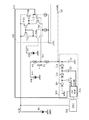
特許文献1には、スイッチング時のノイズ発生を抑制することができるDC/DCコンバータが記載されている。図5は、特許文献1に記載されている昇圧回路の技術を説明するために、特許文献1に記載されている内容に発明者が手を加えて作成した参考例1による昇圧回路の回路ブロック図である。
図5を引用して参考例1による昇圧回路の構成と動作について説明する。図5に記載の昇圧回路は、グランド電位GNDに対して正の電圧VDDを出力する電源301を用いてグランド電位GNDより低い負の電圧を昇圧する昇圧回路である。この参考例1の昇圧回路では、電源301から電源電圧VDDが発振回路302と電圧比較用アンプ106に供給される。チャージポンプ回路303は発振回路302の出力するクロック信号と電圧比較用アンプ106の出力する制御電圧Vn2とに基づいて昇圧動作を行い、出力端子107から負に(電圧の絶対値が)昇圧された電圧VCPLを出力する。図5の昇圧回路では、出力電圧VCPLを安定化させるために、第1の基準電圧Vr1と第2の基準電圧Vr2を用いて電圧比較用アンプ106の出力する制御電圧Vn2を制御し、制御電圧Vn2の電圧値によってチャージポンプ回路303の動作をさらに制御している。
The configuration and operation of the booster circuit according to Reference Example 1 will be described with reference to FIG. The booster circuit shown in FIG. 5 is a booster circuit that boosts a negative voltage lower than the ground potential GND using a
具体的には、出力端子107と第1の基準電圧Vr1を出力する基準電圧源104との間に直列に接続された抵抗R2、R1を設け、そのR2、R1の接続点の第1ノードVn1を電圧比較用アンプ106の非反転入力端子へ接続している。電圧比較用アンプ106の反転入力端子には、別の基準電圧源105が出力する第2の基準電圧Vr2が接続される。この構成により、電圧比較用アンプ106及びチャージポンプ回路303全体で負帰還がかかっており、第1ノードの電圧Vn1と第2の基準電圧Vr2の電圧値が等しくなるようにチャージポンプ回路303の昇圧電圧を制御している。
Specifically, resistors R2 and R1 connected in series are provided between the
この動作についてさらに詳しく説明する。発振回路302から出力された一定のパルス波はチャージポンプ回路(昇圧回路)303へと入力されて、昇圧動作により昇圧された電圧が電圧出力端子107から出力される。電圧出力端子107と基準電圧源104との間に接続されたR1、R2からなる電圧検出回路には、以下の式(1)で示す電流In1が流れる。
This operation will be described in more detail. The constant pulse wave output from the
In1=(Vr1−VCPL)/(R1+R2) 式(1) In1 = (Vr1-VCPL) / (R1 + R2) Formula (1)
よって、R1とR2の接続点の電位Vn1は、式(2)式で表される。 Therefore, the potential Vn1 at the connection point between R1 and R2 is expressed by Expression (2).
Vn1=Vr1−R2×In1=Vr1−(R2/(R1+R2))×(Vr1−VCPL) 式(2) Vn1 = Vr1-R2 * In1 = Vr1- (R2 / (R1 + R2)) * (Vr1-VCPL) Formula (2)
ここで、電圧比較用アンプ106に入力されるVn1、Vr2は、Vn1=Vr2となるような動作をするので、式(3)が成立する。
Here, since Vn1 and Vr2 input to the
Vn1=Vr1−(R2/(R1+R2))×(Vr1−VCPL)=Vr2 式(3) Vn1 = Vr1− (R2 / (R1 + R2)) × (Vr1−VCPL) = Vr2 Equation (3)
式(3)を整理すると式(4)が得られる。 When formula (3) is rearranged, formula (4) is obtained.
VCPL=Vr1−((R1+R2)/R2)×(Vr1−Vr2) 式(4) VCPL = Vr1 − ((R1 + R2) / R2) × (Vr1−Vr2) Formula (4)
式(4)によれば、昇圧回路の出力電圧VCPLは、第1、第2の基準電圧Vr1、Vr2の電圧値と抵抗R1、R2の抵抗値によって決定され、その値は常に一定となることが分かる。 According to equation (4), the output voltage VCPL of the booster circuit is determined by the voltage values of the first and second reference voltages Vr1 and Vr2 and the resistance values of the resistors R1 and R2, and the value is always constant. I understand.
特許文献2には、別の昇圧回路が記載されている。図7は、特許文献2に記載されている技術内容を発明者がさらに補って作成した参考例2による昇圧回路の回路ブロック図である。図7を用いてこの参考例2による昇圧回路の構成と動作について説明する。電源301からは電源電圧VDDが、発振回路302と電圧電流変換回路(OTA)205、バッファ回路207に供給される。電圧電流変換回路(OTA)205は、第1のノードVn1の電圧と基準電圧VSSとを入力し、第1のノードVn1の電圧と基準電圧VSSとの電位差を電流に変換し、出力電流Ioとして出力する。第1のノードVn1は、電圧出力端子207から出力される出力電圧VCPLと基準電圧生成回路204が出力する基準電圧Vr/nとを抵抗Rと抵抗nRとで抵抗分割したノードである。さらに、電圧電流変換回路205の出力電流Ioをチャージする入力容量Cinを備え、入力容量Cinにチャージされた出力電流Ioは、電圧Vn2iを発生させて、バッファ回路212へと入力される。バッファ回路212は入力電圧信号Vn2iと電圧値が同一で出力インピーダンスが低い制御電圧信号Vn2として出力する。この制御電圧信号Vn2は、チャージポンプ回路303に供給され、チャージポンプ回路303の昇圧動作を制御する。また、チャージポンプ回路303には、発振回路302の出力信号が入力し、この発振回路の出力信号に基づくチャージポンプ回路303の昇圧動作を制御電圧信号Vn2の電圧値で制御することによりチャージポンプ回路303の出力電圧VCPLの安定化を図っている。図8に電圧電流変換回路(OTA)205の内部回路図、図9にバッファ回路212の内部回路図を示す。
図7に示す参考例2において、第1のノードの電圧値Vn1は、以下に示す式(5)で表される。 In Reference Example 2 shown in FIG. 7, the voltage value Vn1 of the first node is expressed by the following equation (5).
Vn1=(VCPL−(VCPL−(Vr/n))/(R+nR))×nR
=VCPL−((VCPL×nR−Vr×R)/(R+nR)) 式(5)
Vn1 = (VCPL− (VCPL− (Vr / n)) / (R + nR)) × nR
= VCPL − ((VCPL × nR−Vr × R) / (R + nR)) Equation (5)
式(5)をさらに変形すると、式(6)を経由して、式(7)が得られる。 When Formula (5) is further modified, Formula (7) is obtained via Formula (6).
Vn1×(R+nR)=VCPL×(R+nR)−(VCPL×nR−Vr×R)
=VCPL×R+Vr×R 式(6)
Vn1 × (R + nR) = VCPL × (R + nR) − (VCPL × nR−Vr × R)
= VCPL × R + Vr × R Formula (6)
Vn1=((VCPL+Vr)×R)/((1+n)×R)
=(VCPL+Vr)/(1+n) 式(7)
Vn1 = ((VCPL + Vr) × R) / ((1 + n) × R)
= (VCPL + Vr) / (1 + n) Equation (7)
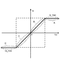
次に、図7に示す参考例2の動作について説明する。電圧電流変換回路205は、入力端子に入力される電位差Vd(=Vn1−VSS)によってその出力電流Ioのレベルが変わる特性を有するが、電位差Vdが一定電圧範囲内にあれば、出力電流Ioは電位差Vdに比例して発生する線形的な特性を有し、電位差Vdが一定範囲を逸脱すれば、電位差Vdに関係なく最大出力電流Io_maxとして発生する飽和特性を有する。この電圧電流変換回路205の出力電流特性を図10の電圧電流特性図に示す。図10は横軸に第1のノードVn1と基準電圧VSSとの電位差Vd=Vn1−Vssをプロットし、縦軸に出力電流Ioをプロットしている。電位差Vdが正の場合(図10中のA及びBの電圧範囲)は出力電圧VCPLが目標電圧Vrよりも高い(絶対値が低い)場合の出力電流Ioを示し、電位差Vdが負の場合(図10中のC及びDの電圧範囲)は出力電圧VCPLが目標電圧Vrよりも低い(絶対値が高い)場合の出力電流Ioを示している。
Next, the operation of Reference Example 2 shown in FIG. 7 will be described. The voltage-
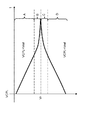
また、電圧電流変換回路205に入力される電位差Vdにより出力電流Ioの値は決定されるが、電圧範囲B、Cを例に取ると、出力電圧VCPLが目標電圧Vrに近くなるにつれて、電位差Vdが小さくなる為、Vn2i、Vn2および出力電圧VCPLの上昇量も減少する。従って、図10のA〜Dの電圧範囲それぞれの時間tに対する出力電圧VCPLの特性は、図11のようになる。例えば、出力電圧VCPLが目標電圧Vrより僅かに電位が低くなった場合、電位差が小さい為Vn2i、Vn2の上昇速度を低下させて、それに応じて出力電圧VCPLの上昇速度も低下するので、目標電圧Vr付近のリップルを最小化させることが可能となる。なお、図7において、基準電圧VSS、Vr/nの電圧値、抵抗R、nRの比率、電圧電流変換回路205への非反転入力端子と反転入力端子との接続を買えることにより、図7の昇圧回路の昇圧電圧は正電圧出力、負電圧出力のどちらに用いることもできる。
The value of the output current Io is determined by the potential difference Vd input to the voltage-
また、特許文献3には、特許文献3の図1を参照すると、昇圧電圧の大きさを検知して発振器の動作状態を制御する電圧検知回路15に加えて昇圧回路の出力と昇圧回路の負荷回路10との間に負荷回路の動作状態を検出する機能を有する回路16を接続することにより、その検出結果により昇圧回路の電流供給能力を能動的に調整する機能を有する半導体集積回路が記載されている。
In Patent Document 3, referring to FIG. 1 of Patent Document 3, in addition to the voltage detection circuit 15 that detects the magnitude of the boost voltage and controls the operating state of the oscillator, the output of the boost circuit and the load of the boost circuit A semiconductor integrated circuit having a function of actively adjusting a current supply capability of a booster circuit based on a detection result by connecting a circuit 16 having a function of detecting an operation state of a load circuit between the
さらに、特許文献4には、特許文献4の図1を参照すると、入力端子7と出力端子9の間に第1と第2の整流素子10、11が直列に接続され、電荷がそれらの整流素子10、11を順に移動して出力コンデンサ12に蓄積されることにより出力端子9から所定の電圧を出力するものにおいて、出力端子9からの帰還電圧と基準電圧の差を積分する積分器15と、第1と第2の整流素子10、11の接続点に一端が接続されたブースト用コンデンサ17と、クロック信号CLKが入力される電源側及び接地側のトランジスタ30、31とそのいずれかに積分器15の出力電圧に応じた電流を流す可変電流源32とを有してブースト用コンデンサ17の他端に出力が接続されるクロック反転器16と、を備え、
負荷が軽い場合でも出力電圧のリップルの周期が短くリップル電圧が小さいチャージポンプ回路1が記載されている。
Further, in Patent Document 4, referring to FIG. 1 of Patent Document 4, first and
The
特許文献5には、特許文献5の図1を参照すると、昇圧回路の出力を基準電圧と比較し、その誤差信号で充電回路を形成するスイッチングトランジスタの少なくとも一方の導通時の抵抗値を変えて第1コンデンサの充電を制御するようにしたチャージポンプ式昇圧回路が記載されている。 In Patent Document 5, referring to FIG. 1 of Patent Document 5, the output of the booster circuit is compared with a reference voltage, and the resistance value at the time of conduction of at least one of the switching transistors forming the charging circuit is changed by the error signal. A charge pump booster circuit is described which controls the charging of the first capacitor.
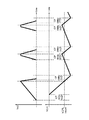
以下の分析は本発明により与えられる。参考例1では、図6に参考例1の電圧比較用アンプ106の出力する制御電圧Vn2と出力端子107から出力される出力電圧VCPLの出力波形を示すとおり、電圧比較用アンプ106の応答速度に比べて、チャージポンプ回路303の充放電時間が非常にゆっくりとしたものであるために、応答遅れ(Delay)が生じ、結果として電圧比較用アンプ106の出力する制御電圧Vn2及び出力端子107から出力される出力電圧VCPLに大きなリップル電圧が現れることである。この応答遅れの為に、余計に昇圧してしまい、結果としてリップル電圧が大きくなる。このリップル電圧が大きいと他の回路の安定した動作が阻害される。
The following analysis is given by the present invention. In the reference example 1, the response speed of the
一方、参考例2では、チャージポンプ回路の出力電圧VCPLが目標電圧に近づくにつれてチャージポンプ回路の昇圧能力が一定になるように制御するので、比較例1に比べるとリップル電圧を小さくすることができる。しかし、参考例2では、電圧電流変換回路の出力電流を積分して電圧に変換するために容量Cinが必要であり、チャージポンプ回路全体の応答速度を考えると容量Cinの容量値をある程度大きくする必要がある。昇圧回路全体の半導体集積回路化を考える場合には、一般的に大きな容量値を少ない面積で集積化することが困難である。また、特許文献1乃至5には、全体を半導体集積回路化したときに、少ない面積で安定した出力電圧を得ることができる昇圧回路は記載されていない。
On the other hand, in the reference example 2, since the boosting capability of the charge pump circuit is controlled to be constant as the output voltage VCPL of the charge pump circuit approaches the target voltage, the ripple voltage can be reduced as compared with the comparative example 1. . However, in the reference example 2, the capacitor Cin is necessary to integrate the output current of the voltage-current converter circuit and convert it into a voltage. Considering the response speed of the entire charge pump circuit, the capacitance value of the capacitor Cin is increased to some extent. There is a need. When considering a semiconductor integrated circuit for the entire booster circuit, it is generally difficult to integrate a large capacitance value with a small area. Further,
本発明の1つの側面による昇圧回路は、クロック信号に基づいて昇圧を行うチャージポンプ回路と、前記チャージポンプ回路の出力電圧に比例する電圧と基準電圧とが初段の非反転入力信号と反転入力信号として入力され、前段の差動出力信号と基準電圧とが後段の非反転入力信号と反転入力信号として入力され、最終段の差動出力信号が前記チャージポンプ回路の動作制御電圧信号として前記チャージポンプ回路の動作を制御する縦続接続された複数の差動増幅回路と、を備え、前記縦続接続された複数の差動増幅回路は、各段の差動出力信号が当該段の反転入力信号として帰還されるようにそれぞれ負帰還接続されている。 A booster circuit according to one aspect of the present invention includes a charge pump circuit that performs boosting based on a clock signal, a voltage that is proportional to an output voltage of the charge pump circuit, and a reference voltage that are first-stage non-inverted input signal and inverted input signal. The differential output signal of the previous stage and the reference voltage are input as the non-inverted input signal and the inverted input signal of the subsequent stage, and the differential output signal of the final stage is used as the operation control voltage signal of the charge pump circuit. A plurality of cascaded differential amplifier circuits for controlling the operation of the circuit, wherein the plurality of cascaded differential amplifier circuits feed back the differential output signal of each stage as the inverted input signal of the stage. Each is connected with negative feedback.
また、本発明の他の側面による半導体集積回路は、上記昇圧回路が単一の半導体基板の上に形成されている。 In the semiconductor integrated circuit according to another aspect of the present invention, the booster circuit is formed on a single semiconductor substrate.
本発明によれば、縦続接続された複数の差動増幅回路は、全体としてチャージポンプ回路の出力電圧が一定になるようにチャージポンプ回路を制御するとともに、縦続接続された複数の差動増幅回路は、各段の差動出力信号が当該段の反転入力信号として帰還されるようにそれぞれ負帰還接続されているので、出力電圧の変化を緩和させ、安定化させることができる。また、出力電圧の安定化のために大きな容量を必要としないので、半導体集積回路化した場合に面積を小さくすることができる。 According to the present invention, the plurality of cascaded differential amplifier circuits controls the charge pump circuit so that the output voltage of the charge pump circuit becomes constant as a whole, and the plurality of cascaded differential amplifier circuits Since the differential output signal of each stage is negatively feedback-connected so that it is fed back as the inverted input signal of that stage, the change in the output voltage can be relaxed and stabilized. Further, since a large capacity is not required for stabilizing the output voltage, the area can be reduced when a semiconductor integrated circuit is formed.
本発明の実施形態の概要について、必要に応じて図面を参照して説明する。なお、概要の説明において引用する図面及び図面の符号は実施形態の一例として示すものであり、それにより本発明による実施形態のバリエーションを制限するものではない。 An outline of an embodiment of the present invention will be described with reference to the drawings as necessary. In the description of the outline, the drawings and the reference numerals of the drawings are shown as examples of the embodiments, and the variations of the embodiments according to the present invention are not limited thereby.
一実施形態の昇圧回路300、300A、300Bは、一例を図1、図4、図12に示すように、クロック信号に基づいて昇圧を行うチャージポンプ回路303、303Aと、チャージポンプ回路303、303Aの出力電圧VCPL、VCPLAに比例する電圧Vn1、Vn1Aと基準電圧Vr1、Vr1Aとが初段の非反転入力信号と反転入力信号として入力され、前段の差動出力信号Vn3と基準電圧Vr1、Vr1Aとが後段の非反転入力信号と反転入力信号として入力され、最終段の差動出力信号(制御電圧Vn2)がチャージポンプ回路303、303Aの動作制御電圧信号としてチャージポンプ回路303、303Aの動作を制御する縦続接続された複数の差動増幅回路(309または309Aと、311)と、を備え、縦続接続された複数の差動増幅回路(309または309Aと、311)は、各段の差動出力信号が当該段の反転入力信号として帰還されるようにそれぞれ負帰還接続されている(309、309A、311の差動出力端子は、それぞれ抵抗R6、R6A、R4を介してそれぞれの反転入力端子に接続)。
The boosting circuits 300, 300A, and 300B according to the embodiment include
また、一実施形態の昇圧回路300、300A、300Bは、発振回路302を更に備え、チャージポンプ回路303、303Aは、発振回路302の発振周波数に基づいて振幅が最終段の差動出力信号(制御電圧Vn2)により制御されるクロック信号を生成するクロックバッファ313(図2参照)を備え、クロックバッファ313が出力するクロック信号の電圧振幅に基づいてチャージポンプ回路303、303Aの昇圧能力が制御されることが好ましい。
Further, the booster circuits 300, 300A, and 300B of the embodiment further include an
また、基準電圧Vr1、Vr1Aを第1の基準電圧としたときに、第1の基準電圧Vr1、Vr1Aと第2の基準電圧Vr2、Vr2Aとを出力する基準電圧生成回路304、304Aを更に備え、第2の基準電圧Vr2、Vr2Aとチャージポンプ回路303、303Aの出力電圧とを抵抗分圧した電圧Vn1、Vn1Aがチャージポンプ回路303、303Aの出力電圧に比例する電圧として初段309、309Aに入力されることが好ましい。
Further, when the reference voltages Vr1 and Vr1A are used as the first reference voltage, reference
また、図1に一例を示すように、初段309の前段にさらにユニティゲインアンプ306を備え、チャージポンプ回路303の出力電圧VCPLに比例する電圧Vn1がユニティゲインアンプ306を介してインピーダンス変換されて初段309に入力されることが好ましい。
In addition, as shown in FIG. 1, a
また、図1、図4に一例を示すように、チャージポンプ回路303が負電圧の絶対値が大きくなるように昇圧して出力するチャージポンプ回路303であって、縦続接続された複数の差動増幅回路309、311は全体として、チャージポンプ回路303の出力電圧VCPLに比例する電圧Vn1が、下降すればチャージポンプ回路303の昇圧能力を減少させ、上昇すればチャージポンプ回路303の昇圧能力を増加させるように接続されていることが好ましい。
Further, as shown in FIG. 1 and FIG. 4, the
また、図12に一例を示すように、チャージポンプ回路が正電圧を昇圧して出力するチャージポンプ回路303Aであって、縦続接続された複数の差動増幅回路309A、311は全体として、前記チャージポンプ回路の出力電圧VCPLに比例する電圧Vn1Aが、上昇すればチャージポンプ回路303Aの昇圧能力を減少させ、下降すればチャージポンプ回路303Aの昇圧能力を増加させるように接続されていることが好ましい。
Further, as shown in FIG. 12, the
また、図4に一例を示すように、昇圧回路300Aは、チャージポンプ回路303の電圧出力端子VCPLと、第1のノードVn1と、の間に接続された第1の抵抗R1と、基準電圧生成回路304の第2の基準電圧Vr2を出力する第2基準電圧出力端子315と、第1のノードVn1と、の間に接続された第2の抵抗R2と、をさらに備え、複数縦続接続された差動増幅回路309、311は、第1の差動増幅回路309と、第1の差動増幅回路309の差動出力端子Vn3が第3の抵抗R3を介して反転入力端子に接続され、差動出力端子と反転入力端子が第4の抵抗R4を介して接続され、第1の基準電圧Vr1を出力する基準電圧生成回路304の第1基準電圧出力端子305が非反転入力端子310に接続され、差動出力端子がクロックバッファ313の電源端子Vn2IN(図2参照)に接続された第2の差動増幅回路311と、を備え、第1の差動増幅回路309は、反転入力端子が第5の抵抗R5を介して第1のノードVn1に接続されるとともに、第6の抵抗R6を介して当該差動増幅回路309の差動出力端子Vn3に接続され、非反転入力端子308が第1基準電圧出力端子305に接続されていることが好ましい。
Further, as shown in FIG. 4, the booster circuit 300A includes a first resistor R1 connected between the voltage output terminal VCPL of the
また、図1に一例を示すように、チャージポンプ回路303の電圧出力端子VCPLと、第1のノードVn1と、の間に接続された第1の抵抗R1と、第2の基準電圧Vr2を出力する基準電圧生成回路304の第2基準電圧出力端子315と、第1のノードVn1と、の間に接続された第2の抵抗R2と、非反転入力端子が第1のノードVn1に接続され、反転入力端子が差動出力端子に接続されたユニティゲインアンプ306と、をさらに備え、複数縦続接続された差動増幅回路(309と311)は、第1の差動増幅回路309と、第1の差動増幅回路309の差動出力端子Vn3が第3の抵抗R3を介して反転入力端子に接続され、差動出力端子と反転入力端子が第4の抵抗R4を介して接続され、第1の基準電圧Vr1を出力する基準電圧生成回路304の第1基準電圧出力端子305が非反転入力端子310に接続され、差動出力端子がクロックバッファ313の電源端子(図2のVn2IN)に接続された第2の差動増幅回路311と、を備え、第1の差動増幅回路309は、反転入力端子が第5の抵抗R5を介してユニティゲインアンプ306の差動出力端子に接続されるとともに、第6の抵抗R6を介して当該差動増幅回路309の差動出力端子に接続され、非反転入力端子308が第1基準電圧出力端子305に接続されていることが好ましい。
Further, as shown in FIG. 1, the first resistor R1 connected between the voltage output terminal VCPL of the
また、上記昇圧回路300、300A、300Bが単一の半導体基板の上に形成されていることが好ましい。 The booster circuits 300, 300A, and 300B are preferably formed on a single semiconductor substrate.
以上で概要の説明を終了し、より具体的な実施例について、図面を参照して詳しく説明する。 The description of the outline is finished above, and more specific embodiments will be described in detail with reference to the drawings.
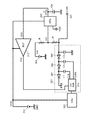
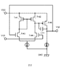
図1は、実施例1による昇圧回路全体の回路ブロック図である。図1における昇圧回路300の構成について説明する。電源301は、発振回路302、基準電圧生成回路304、ユニィティゲインアンプ306、差動増幅回路309、311に電源電圧VDDを供給する。発振回路302は、クロック信号を生成し、チャージポンプ回路303に供給する。チャージポンプ回路303はそのクロック信号を受けて昇圧動作を行う。昇圧回路303の出力電圧信号VCPLは、昇圧回路300全体の出力端子である電圧出力端子307から出力される。また、基準電圧生成回路304は、昇圧回路300の昇圧動作の基準電圧となる第1の基準電圧Vr1と第2の基準電圧Vr2とをそれぞれ第1基準電圧出力端子305と第2基準電圧出力端子315から出力する。第2基準電圧出力端子315と電圧出力端子307とは、直列に接続された抵抗R2とR1を介して接続されている。第2基準電圧出力端子315から出力される電圧Vr2と電圧出力端子307の出力電圧VCPLとを抵抗R2と抵抗R1で抵抗分割することにより、抵抗R2と抵抗R1の接続点(中間点)である第1のノードVn1に出力電圧VCPLに比例する電圧(または、第2基準電圧出力端子315から出力される基準電圧と出力電圧VCPLとの電位差に比例する電圧)が得られる。
FIG. 1 is a circuit block diagram of the entire booster circuit according to the first embodiment. A configuration of the booster circuit 300 in FIG. 1 will be described. The
ユニティゲインアンプ306は、非反転入力端子が第1のノードVn1に接続され、反転入力端子と差動出力端子が直接接続された差動増幅回路により構成される。このユニティゲインアンプ306により第1のノードVn1と同一電圧であって低インピーダンスである出力信号がユニティゲインアンプ306の出力端子(差動増幅回路の差動出力端子)から出力される。ユニティゲインアンプ306の出力信号は、直列に縦続接続された複数の差動増幅回路309、311に入力される。縦続接続された複数の差動増幅回路309、311には、第1の基準電圧Vr1が入力されており、ユニティゲインアンプ306によって低インピーダンスにインピーダンス変換された第1のノードVn1の電位が第1の基準電圧Vr1と比較され、その比較結果に基づいて制御電圧Vn2が縦続接続された差動増幅回路309、311の最終段311の差動出力端子から出力される。この制御電圧Vn2は、昇圧回路303のクロックバッファ313に電源として供給される。制御電圧Vn2の電圧値は、クロックバッファ313から出力されるクロック信号の振幅値を制御する。
The
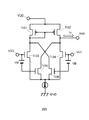
図2は、このクロックバッファ313の内部回路図である。図2のVn2INは制御電圧Vn2を出力する差動増幅回路311の非反転出力端子に接続される。また、OCNIN端子は、発振回路302の出力信号に接続され、GNDはグランド端子に接続される。図2に示すクロックバッファ313によって発振回路302の出力するクロック信号は振幅のロウレベルがグランドGNDレベル、振幅のハイレベルがVn2であるクロック信号CLK、及びCLKと位相が反転して振幅が同一である信号CLKB、に変換されて出力する。
FIG. 2 is an internal circuit diagram of the
図1に戻って、昇圧回路303は、このクロックバッファ313が出力するクロック信号CLK、CLKBにそれぞれ一端が接続された容量C1、C2と、電圧出力端子307と接地GNDとの間に接続された容量C3と、電圧出力端子307と接地GNDとの間に直列に接続されたダイオードDi3、Di2、Di3によって構成されている。ダイオードDi3のアノードは電圧出力端子307に接続され、ダイオードDi3のカソードとダイオードDi2のアノードは容量C2の他端に接続され、ダイオードDi2のカソードとダイオードDi1のアノードは容量C1の他端に接続され、タイオードDi1のカソードはグランド端子GNDに接続されている。
Returning to FIG. 1, the
次に、縦続接続された複数の差動増幅回路309、311について、内部の接続について説明する。初段(前段)の差動増幅回路309の反転入力端子はユニティゲインアンプ306の出力端子と抵抗R5を介して接続されている。また、初段の差動増幅回路309の反転入力端子と差動出力端子は抵抗R6を介して接続され、非反転入力端子308は基準電圧生成回路304の第1基準電圧出力端子305に接続されている。出力端子と反転入力端子とを接続する抵抗R6はこの演算増幅回路309の負帰還回路として機能する。この構成により、初段の差動増幅回路309は、ユニティゲインアンプ306の出力信号(第1のノードVn1と同電位の信号)と第1の基準電圧Vr1との電位差を抵抗R5と抵抗R6との抵抗値の比によって反転して出力する反転増幅回路として機能する。
Next, internal connections of the plurality of
後段(最終段)の差動増幅回路311は、反転入力端子が前段の差動増幅回路309の差動出力端子と抵抗R3を介して接続され、反転入力端子と差動出力端子は抵抗R4を介して接続され、非反転入力端子310には基準電圧生成回路311の第1基準電圧出力端子305が接続されている。差動出力端子と反転入力端子とを接続する抵抗R4はこの演算増幅回路311の負帰還回路として機能する。この構成により、最終段の差動増幅回路311は、前段の差動増幅回路309から出力される信号Vn3と第1の基準電圧Vr1との電位差を抵抗R3と抵抗R4との抵抗値の比によって反転して出力する反転増幅回路として機能する。
The
すなわち、縦続接続された差動増幅回路309、311全体では、初段309で反転した信号を最終段311でさらに反転しているので、全体としては、ユニティゲインアンプ306の出力信号(Vn1と同一電位)と第1の基準電位Vr1との電位差を増幅率(R6/R5)*(R4/R3)で増幅して出力する非反転増幅回路として機能する。
That is, in the cascaded
次に、この昇圧回路の動作について説明する。図1において、抵抗R1、R2に流れる電流In1は以下の式(11)により求められる。 Next, the operation of this booster circuit will be described. In FIG. 1, the current In1 flowing through the resistors R1 and R2 is obtained by the following equation (11).
In1=(Vr2−VCPL)/(R1+R2) 式(11) In1 = (Vr2-VCPL) / (R1 + R2) Formula (11)
R1とR2の間の電位Vn1は、式(12)により求められる。 The potential Vn1 between R1 and R2 is obtained by the equation (12).
Vn1=Vr2−(R2/(R1+R2))×(Vr2−VCPL)
=(1/(R1+R2))×(R1×Vr2+R2×VCPL) 式(12)
Vn1 = Vr2- (R2 / (R1 + R2)) * (Vr2-VCPL)
= (1 / (R1 + R2)) × (R1 × Vr2 + R2 × VCPL) Equation (12)
ユニティゲインアンプ(電圧比較用アンプ)306の動作により、第1のノードVn1とユニティゲインアンプ306の出力は同一電位となり、差動増幅回路309の出力電圧をVn3とすると、以下の式(13)が成立する。
The operation of the unity gain amplifier (voltage comparison amplifier) 306 causes the output of the first node Vn1 and the
(Vr1−Vn1)/R5=(Vn3−Vr1)/R6 式(13) (Vr1-Vn1) / R5 = (Vn3-Vr1) / R6 Formula (13)
式(13)において、R5=R6とすると式(14)が得られる。 In the equation (13), when R5 = R6, the equation (14) is obtained.
Vn3=−Vn1+2Vr1 式(14) Vn3 = −Vn1 + 2Vr1 Formula (14)
また、差動増幅回路309と同様に、差動増幅回路311の出力電圧(制御電圧)をVn2とすると以下の式(15)が成立する。
Similarly to the
((Vr1−Vn3)/R3)=((Vn2−Vr1)/R4) 式(15) ((Vr1-Vn3) / R3) = ((Vn2-Vr1) / R4) Formula (15)
式(15)を、Vn2について解くと、式(16)が得られる。 When equation (15) is solved for Vn2, equation (16) is obtained.
Vn2=(R4/R3)×(Vr1−Vn3)+Vr1
=((R3+R4)/R3)×Vr1−(R4/R3)×Vn3 式(16)
Vn2 = (R4 / R3) × (Vr1−Vn3) + Vr1
= ((R3 + R4) / R3) * Vr1- (R4 / R3) * Vn3 Formula (16)
上記式(16)に式(14)を代入すると以下の式(17)が得られる。 Substituting equation (14) into equation (16) above yields equation (17) below.
Vn2=((R3+R4)/R3)×Vr1−(R4/R3)×(−Vn1+2Vr1)
=((R3+R4)/R3)×Vr1+(R4/R3)×Vn1−(2R4/R3)×Vr1
=((R3−R4)/R3)×Vr1+(R4/R3)×Vn1 式(17)
Vn2 = ((R3 + R4) / R3) × Vr1− (R4 / R3) × (−Vn1 + 2Vr1)
= ((R3 + R4) / R3) * Vr1 + (R4 / R3) * Vn1- (2R4 / R3) * Vr1
= ((R3-R4) / R3) * Vr1 + (R4 / R3) * Vn1 Formula (17)
上記式(17)に式(12)を代入すると以下の式(18)が得られる。 Substituting equation (12) into equation (17) yields the following equation (18).
Vn2=((R3−R4)/R3)×Vr1+(R4/R3)×((1/(R1+R2))×(R1×Vr2+R2×VCPL)) 式(18) Vn2 = ((R3−R4) / R3) × Vr1 + (R4 / R3) × ((1 / (R1 + R2)) × (R1 × Vr2 + R2 × VCPL)) Formula (18)
上記式(18)において、A=Vr2/Vr1とおくと、式(19)が得られる。 In the above equation (18), when A = Vr2 / Vr1, the equation (19) is obtained.
Vn2=Vr1×(((R3‐R4)/R3)+((A×R1)/(R1+R2))×(R4/R3))+(R4/R3)×(R2/(R1+R2))×VCPL 式(19) Vn2 = Vr1 × (((R3-R4) / R3) + ((A × R1) / (R1 + R2)) × (R4 / R3)) + (R4 / R3) × (R2 / (R1 + R2)) × VCPL Formula (19)
上記式(19)に示すとおり、Vn2を求める式の成分の中に、VCPLと一定の係数を含ませることによって、VCPLに対するVn2の傾きを緩やかにすることが出来る。
よって、図1の回路構成を採ることにより、VCPLの安定化とリップル電圧を抑える効果が得られる。
As shown in the above equation (19), the slope of Vn2 with respect to VCPL can be made gentle by including VCPL and a constant coefficient in the component of the equation for obtaining Vn2.
Therefore, the effect of stabilizing the VCPL and suppressing the ripple voltage can be obtained by adopting the circuit configuration of FIG.
次に、図3に図1の昇圧回路における縦続接続された差動増幅回路の最終段311が出力する制御電圧(クロックバッファの電源電圧)Vn2と昇圧回路全体の出力電圧VCPLとの波形図の一例を示す。横軸は時間tである。図1の昇圧回路300は負電圧を出力する昇圧回路であるので、出力電圧VCPLがVCPLの目標電圧VCPLtargetより高い高電圧(絶対値が低い電圧)である場合は、チャージポンプ回路303の昇圧能力が不足しているので、制御電圧Vn2の電圧を高くしてチャージポンプ回路303の昇圧能力を高めるように制御する。一方、チャージポンプ回路303の昇圧した電圧VCPLが目標電圧VCPLtargetを超えた場合(VCPLがVCPLtargetより低い電圧になった場合)は、制御電圧Vn2の電圧を低くしてチャージポンプ回路303の昇圧能力を緩めるように制御する。ただし、チャージポンプ回路303はその回路の特性として、制御電圧Vn2を変化させても、すぐには出力電圧VCPLには反映されず、一定時間(CPdelay)遅れてから始めて出力電圧VCPLに反映される。
Next, FIG. 3 is a waveform diagram of the control voltage (clock buffer power supply voltage) Vn2 output from the
しかし、実施例1によれば、縦続接続された差動増幅回路309、311には、それぞれ差動増幅回路毎に差動出力端子から出力される信号が反転入力信号に帰還されるように負帰還接続されている。具体的には、差動増幅回路309の差動出力端子は抵抗R6を介して反転入力端子に負帰還接続され、差動増幅回路311の差動出力端子は抵抗R4を介して反転入力端子に負帰還接続されている。したがって、制御電圧Vn2の急激な変化が抑制される。特に、出力電圧VCPLと目標電圧VCPLtargetとの電位差が小さくなればなるほど、制御電圧Vn2の変化は緩慢になる。したがって、制御電圧Vn2の変化に対して、出力電圧VCPLの変化が一定時間(CPdelay)遅れたとしても、出力電圧VCPLに大きなリップルが乗ることはない。
However, according to the first embodiment, the
比較のため、図6に示す参考例1(図5)の昇圧回路の制御電圧Vn2と出力電圧VCPLの波形図を再度参照する。参考例1では、出力電圧VCPLの電圧値に比例する電圧Vn1が電圧比較用アンプ106の非反転入力端子に接続され、全体として負帰還が係っているが、電圧比較用アンプ106固有の帰還系は設けていない。したがって、出力電圧VCPLが目標電圧VCPLtargetより高いか低いかによって、制御電圧Vn2の電圧値は大きく変化し、出力電圧VCPLの変化が一定時間(CPdelay)遅れるとその間に出力電圧VCPLが目標電圧VCPLtargetから大きくずれてしまうので、出力電圧VCPLにリップルが乗ることは避けられない。
For comparison, reference is again made to the waveform diagrams of the control voltage Vn2 and the output voltage VCPL of the booster circuit of Reference Example 1 (FIG. 5) shown in FIG. In the reference example 1, the voltage Vn1 proportional to the voltage value of the output voltage VCPL is connected to the non-inverting input terminal of the
また、実施例1では、出力電圧VCPLを検出し、制御電圧Vn2を出力する経路に大きな容量は必要としない。ユニティゲインアンプ306、差動増幅回路309、311内部の容量C4、C5、C6は発振防止用であり、容量値は小さなものでよい。また、チャージポンプ回路303内部の容量C1、C2、C3は昇圧回路として不可欠のものであり、発振回路302の発振周波数と昇圧回路の負荷にもよるが、小さな容量とすることも可能である。したがって、昇圧回路全体や他の機能回路を単一半導体基板の上に集積して半導体集積回路とする場合には、大きな容量を用いないので、昇圧回路自体のレイアウト面積を小さくすることができる。
Further, in the first embodiment, a large capacity is not required for the path for detecting the output voltage VCPL and outputting the control voltage Vn2. The capacitors C4, C5, and C6 in the
図4は、実施例2による昇圧回路300Aの全体の回路ブロック図である。実施例1の昇圧回路300(図1)と比べるとユニティゲインアンプ306を省略し、第1のノードVn1が抵抗R5を介して直接初段の差動増幅回路309の反転入力端子に接続されている。実施例2は実施例1と同様に負電圧を昇圧する昇圧回路である。その他の構成は、実施例1と同一であるので、詳しい回路の構成の説明は省略する。実施例2によれば、第1のノードVn1の電位は、抵抗R5に流れる電流によって影響を受けるが、昇圧回路の出力電圧VCPLが目標電圧VCPLtargetに近い電圧まで昇圧した後は、抵抗R5、抵抗R6には大きな電流が流れなくなるので、第1のノードVn1の電位が抵抗R5に流れる電流によって大きな影響を受けることはない。実施例2によれば、ユニティゲインアンプ306を設ける必要がないので、ユニティゲインアンプ306に流れる電流を削減し、より低消費電流で昇圧回路を動作させることができる。
FIG. 4 is an overall circuit block diagram of the booster circuit 300A according to the second embodiment. Compared with the booster circuit 300 (FIG. 1) of the first embodiment, the
図12は、実施例3による昇圧回路300B全体の回路ブロック図である。実施例3は、図4に示す実施例2の負電圧を出力する昇圧回路300Aを、正電圧を出力する昇圧回路300Bに変更した昇圧回路である。チャージポンプ回路303Aは、ダイオードDi1A〜Di3Aの向きを実施例1、2のタイオードDi1〜Di3とは逆にしてダイオードDi1Aのアノードを電源電圧VDDに接続している。また、昇圧回路300Bの出力端子307Aから第2基準電圧出力端子315Aに流れる電流の向きは実施例1、実施例2とは逆である。また、第1のノードVn1Aは、初段の差動増幅回路309Aの非反転入力端子に接続され、反転入力端子は抵抗R5Aを介して基準電圧生成回路304Aの第1基準電圧出力端子305Aに接続されている。すなわち、初段の差動増幅回路309Aは、増幅率がR6A/R5Aである非反転増幅回路として機能する。実施例3の初段の差動増幅回路309Aの接続も差動出力端子が抵抗R6Aを介して反転入力端子に負帰還接続されている。その他の構成は、実施例1、実施例2と同一であり、実施例1、実施例2と同一の効果が正電圧を出力する昇圧回路においても得られる。
FIG. 12 is a circuit block diagram of the entire booster circuit 300B according to the third embodiment. The third embodiment is a booster circuit in which the booster circuit 300A that outputs a negative voltage in the second embodiment shown in FIG. 4 is changed to a booster circuit 300B that outputs a positive voltage. The
以上、説明した各実施例において、昇圧回路の目標電圧は、基準電圧生成回路304、304Aが出力する第1の基準電圧Vr1、Vr1A、第2の基準電圧Vr2、Vr2Aの電圧値、昇圧回路の出力電圧VCPL、VCPLAと第2の基準電圧Vr2、Vr2Aとを分圧する抵抗の抵抗値の比率により自在に設定することができる。
In each of the embodiments described above, the target voltage of the booster circuit is the first reference voltages Vr1 and Vr1A output from the reference
また、昇圧する電圧を正電圧とするか負電圧とするかについても、チャージポンプ回路の構成と、各段の増幅回路の接続を反転増幅回路として用いるか、非反転増幅回路として用いるかその接続を変える事により、自在に設定することができる。 In addition, regarding whether the voltage to be boosted is a positive voltage or a negative voltage, the configuration of the charge pump circuit and the connection of the amplifier circuit at each stage are used as an inverting amplifier circuit or a non-inverting amplifier circuit. It can be set freely by changing.
また、各実施例のチャージポンプ回路は、整流素子と容量を用いるチャージポンプ回路を例示したが、整流素子をMOSトランジスタ等によるスイッチに代えて、スイッチの導通、非導通をクロックに同期して制御することにより、スイッチを整流素子として使用するチャージポンプ回路を用いてもよいことは言うまでもない。 In addition, the charge pump circuit of each embodiment exemplifies a charge pump circuit that uses a rectifying element and a capacitor. Thus, it goes without saying that a charge pump circuit using a switch as a rectifying element may be used.
また、各実施例では、2段に縦続接続された増幅回路を用いたが、縦続接続する増幅回路の段数は必要に応じて任意の数に変えることができる。 In each embodiment, the amplifier circuits cascaded in two stages are used. However, the number of stages of amplifier circuits cascaded can be changed to any number as necessary.
なお、本発明の全開示(請求の範囲を含む)の枠内において、さらにその基本的技術思想に基づいて、実施形態ないし実施例の変更・調整が可能である。また、本発明の請求の範囲の枠内において種々の開示要素の多様な組み合わせないし選択が可能である。すなわち、本発明は、請求の範囲を含む全開示、技術的思想にしたがって当業者であればなし得るであろう各種変形、修正を含むことは勿論である。 It should be noted that the embodiments and examples can be changed and adjusted within the scope of the entire disclosure (including claims) of the present invention and based on the basic technical concept. Various combinations and selections of various disclosed elements are possible within the scope of the claims of the present invention. That is, the present invention of course includes various variations and modifications that could be made by those skilled in the art according to the entire disclosure including the claims and the technical idea.
104、105、204:基準電圧源
106:電圧比較用アンプ
107、207、307:電圧出力端子
205:電圧電流変換回路(OTA)
212:バッファ
300、300A、300B:昇圧回路
301:電源
302:発振回路
303、303A:チャージポンプ回路
304、304A:基準電圧生成回路
305、305A:第1基準電圧出力端子
306:ユニティゲインアンプ
308、310:第1基準電圧入力端子(非反転入力端子)
309、309A、311:差動増幅回路
313:クロックバッファ
315、315A:第2基準電圧出力端子
321、322:インバータ
C1〜C6、C11、Cin:容量
Di1〜Di3、Di1A〜Di3A:ダイオード
R、R1〜R6、R1A、R2A、R5A、R6A、R11〜R16、R21、R22、nR:抵抗
Tr1〜Tr15、Tr21〜Tr36、Tr41〜Tr45:トランジスタ
VCPL、VCPLA:(昇圧回路の)出力電圧
Vn1、Vn1A:第1のノード
Vr1、Vr1A:第1の基準電圧
Vr2、Vr2A:第2の基準電圧
104, 105, 204: Reference voltage source 106:
212: Buffers 300, 300A, 300B: Booster circuit 301: Power supply 302:
309, 309A, 311: differential amplifier circuit 313:
Claims (9)
前記チャージポンプ回路の出力電圧に比例する電圧と基準電圧とが初段の非反転入力信号と反転入力信号として入力され、前段の差動出力信号と基準電圧とが後段の非反転入力信号と反転入力信号として入力され、最終段の差動出力信号が前記チャージポンプ回路の動作制御電圧信号として前記チャージポンプ回路の動作を制御する縦続接続された複数の差動増幅回路と、
を備え、
前記縦続接続された複数の差動増幅回路は、各段の差動出力信号が当該段の反転入力信号として帰還されるようにそれぞれ負帰還接続されていることを特徴とする昇圧回路。 A charge pump circuit for boosting based on a clock signal;
A voltage proportional to the output voltage of the charge pump circuit and a reference voltage are input as a non-inverting input signal and an inverting input signal in the first stage, and a differential output signal and a reference voltage in the preceding stage are input as a non-inverting input signal and an inverting input in the subsequent stage. A plurality of cascade-connected differential amplifier circuits that control the operation of the charge pump circuit as an operation control voltage signal of the charge pump circuit.
With
The booster circuit, wherein the plurality of cascaded differential amplifier circuits are connected in negative feedback so that a differential output signal of each stage is fed back as an inverted input signal of the stage.
前記チャージポンプ回路は、前記発振回路の発振周波数に基づいて振幅が前記最終段の差動出力信号により制御される前記クロック信号を生成するクロックバッファを備え、前記クロックバッファが出力するクロック信号の電圧振幅に基づいて前記チャージポンプ回路の昇圧能力が制御されることを特徴とする請求項1記載の昇圧回路。 An oscillation circuit;
The charge pump circuit includes a clock buffer that generates the clock signal whose amplitude is controlled by the differential output signal of the final stage based on the oscillation frequency of the oscillation circuit, and the voltage of the clock signal output by the clock buffer 2. The booster circuit according to claim 1, wherein the boosting capability of the charge pump circuit is controlled based on the amplitude.
前記第2の基準電圧と前記チャージポンプ回路の出力電圧とを抵抗分圧した電圧が前記チャージポンプ回路の出力電圧に比例する電圧として前記初段に入力されることを特徴とする請求項1または2記載の昇圧回路。 A reference voltage generation circuit that outputs the first reference voltage and the second reference voltage when the reference voltage is the first reference voltage;
The voltage obtained by resistance-dividing the second reference voltage and the output voltage of the charge pump circuit is input to the first stage as a voltage proportional to the output voltage of the charge pump circuit. The booster circuit described.
前記縦続接続された複数の差動増幅回路は全体として、前記チャージポンプ回路の出力電圧に比例する電圧が、下降すれば前記チャージポンプ回路の昇圧能力を減少させ、上昇すれば前記チャージポンプ回路の昇圧能力を増加させるように接続されていることを特徴とする請求項1乃至4いずれか1項記載の昇圧回路。 The charge pump circuit boosts and outputs the negative voltage so that the absolute value of the negative voltage increases,
The plurality of cascaded differential amplifier circuits as a whole reduces the boosting capability of the charge pump circuit when the voltage proportional to the output voltage of the charge pump circuit decreases, and increases the voltage of the charge pump circuit when the voltage increases. 5. The booster circuit according to claim 1, wherein the booster circuit is connected so as to increase a boosting capability.
前記縦続接続された複数の差動増幅回路は全体として、前記チャージポンプ回路の出力電圧に比例する電圧が、上昇すれば前記チャージポンプ回路の昇圧能力を減少させ、下降すれば前記チャージポンプ回路の昇圧能力を増加させるように接続されていることを特徴とする請求項1乃至4いずれか1項記載の昇圧回路。 The charge pump circuit boosts and outputs a positive voltage;
The plurality of cascaded differential amplifier circuits as a whole reduces the boosting capability of the charge pump circuit when the voltage proportional to the output voltage of the charge pump circuit increases, and decreases the voltage of the charge pump circuit when the voltage decreases. 5. The booster circuit according to claim 1, wherein the booster circuit is connected so as to increase a boosting capability.
前記基準電圧生成回路の前記第2の基準電圧を出力する第2基準電圧出力端子と、前記第1のノードと、の間に接続された第2の抵抗と、
をさらに備え、
前記複数縦続接続された差動増幅回路は、
第1の差動増幅回路と、
前記第1の差動増幅回路の差動出力端子が第3の抵抗を介して反転入力端子に接続され、差動出力端子と前記反転入力端子が第4の抵抗を介して接続され、前記第1の基準電圧を出力する前記基準電圧生成回路の第1基準電圧出力端子が非反転入力端子に接続され、前記差動出力端子が前記クロックバッファの電源端子に接続された第2の差動増幅回路と、
を備え、
前記第1の差動増幅回路は、
反転入力端子が第5の抵抗を介して前記第1のノードに接続されるとともに、第6の抵抗を介して当該差動増幅回路の差動出力端子に接続され、
非反転入力端子が前記第1基準電圧出力端子に接続されていることを特徴とする請求項3記載の昇圧回路。 A first resistor connected between a voltage output terminal of the charge pump circuit and a first node;
A second resistor connected between a second reference voltage output terminal for outputting the second reference voltage of the reference voltage generation circuit and the first node;
Further comprising
The plurality of cascaded differential amplifier circuits are:
A first differential amplifier circuit;
The differential output terminal of the first differential amplifier circuit is connected to an inverting input terminal via a third resistor, the differential output terminal and the inverting input terminal are connected via a fourth resistor, A second differential amplifier in which a first reference voltage output terminal of the reference voltage generation circuit that outputs one reference voltage is connected to a non-inverting input terminal, and the differential output terminal is connected to a power supply terminal of the clock buffer. Circuit,
With
The first differential amplifier circuit includes:
An inverting input terminal is connected to the first node via a fifth resistor, and is connected to a differential output terminal of the differential amplifier circuit via a sixth resistor.
4. The booster circuit according to claim 3, wherein a non-inverting input terminal is connected to the first reference voltage output terminal.
前記第2の基準電圧を出力する前記基準電圧生成回路の第2基準電圧出力端子と、前記第1のノードと、の間に接続された第2の抵抗と、
非反転入力端子が前記第1のノードに接続され、反転入力端子が差動出力端子に接続されたユニティゲインアンプと、
をさらに備え、
前記複数縦続接続された差動増幅回路は、
第1の差動増幅回路と、
前記第1の差動増幅回路の差動出力端子が第3の抵抗を介して反転入力端子に接続され、差動出力端子と前記反転入力端子が第4の抵抗を介して接続され、前記第1の基準電圧を出力する前記基準電圧生成回路の第1基準電圧出力端子が非反転入力端子に接続され、前記差動出力端子が前記クロックバッファの電源端子に接続された第2の差動増幅回路と、
を備え、
前記第1の差動増幅回路は、
反転入力端子が第5の抵抗を介して前記ユニティゲインアンプの差動出力端子に接続されるとともに、第6の抵抗を介して当該差動増幅回路の差動出力端子に接続され、
非反転入力端子が前記第1基準電圧出力端子に接続されていることを特徴とする請求項3記載の昇圧回路。 A first resistor connected between a voltage output terminal of the charge pump circuit and a first node;
A second resistor connected between a second reference voltage output terminal of the reference voltage generation circuit that outputs the second reference voltage and the first node;
A unity gain amplifier having a non-inverting input terminal connected to the first node and an inverting input terminal connected to a differential output terminal;
Further comprising
The plurality of cascaded differential amplifier circuits are:
A first differential amplifier circuit;
The differential output terminal of the first differential amplifier circuit is connected to an inverting input terminal via a third resistor, the differential output terminal and the inverting input terminal are connected via a fourth resistor, A second differential amplifier in which a first reference voltage output terminal of the reference voltage generation circuit that outputs one reference voltage is connected to a non-inverting input terminal, and the differential output terminal is connected to a power supply terminal of the clock buffer. Circuit,
With
The first differential amplifier circuit includes:
An inverting input terminal is connected to a differential output terminal of the unity gain amplifier via a fifth resistor, and is connected to a differential output terminal of the differential amplifier circuit via a sixth resistor.
4. The booster circuit according to claim 3, wherein a non-inverting input terminal is connected to the first reference voltage output terminal.
Priority Applications (1)
| Application Number | Priority Date | Filing Date | Title |
|---|---|---|---|
| JP2010116465A JP5479218B2 (en) | 2010-05-20 | 2010-05-20 | Booster circuit |
Applications Claiming Priority (1)
| Application Number | Priority Date | Filing Date | Title |
|---|---|---|---|
| JP2010116465A JP5479218B2 (en) | 2010-05-20 | 2010-05-20 | Booster circuit |
Publications (2)
| Publication Number | Publication Date |
|---|---|
| JP2011244651A JP2011244651A (en) | 2011-12-01 |
| JP5479218B2 true JP5479218B2 (en) | 2014-04-23 |
Family
ID=45410707
Family Applications (1)
| Application Number | Title | Priority Date | Filing Date |
|---|---|---|---|
| JP2010116465A Expired - Fee Related JP5479218B2 (en) | 2010-05-20 | 2010-05-20 | Booster circuit |
Country Status (1)
| Country | Link |
|---|---|
| JP (1) | JP5479218B2 (en) |
Families Citing this family (2)
| Publication number | Priority date | Publication date | Assignee | Title |
|---|---|---|---|---|
| US11024373B2 (en) | 2019-09-12 | 2021-06-01 | Hefei Reliance Memory Limited | Voltage-mode bit line precharge for random-access memory cells |
| CN113765369B (en) * | 2021-09-01 | 2024-01-23 | 深圳市爱协生科技股份有限公司 | Novel voltage conversion circuit for converting positive voltage into negative voltage in complex power domain |
Family Cites Families (7)
| Publication number | Priority date | Publication date | Assignee | Title |
|---|---|---|---|---|
| JPH0779561A (en) * | 1993-09-10 | 1995-03-20 | Sony Corp | Step-up power supply and booster circuit |
| JPH11219596A (en) * | 1998-02-03 | 1999-08-10 | Nec Corp | Power circuit for semiconductor device |
| JP2001177357A (en) * | 1999-12-17 | 2001-06-29 | Matsushita Electric Works Ltd | Differential amplifier |
| JP3666805B2 (en) * | 2000-09-19 | 2005-06-29 | ローム株式会社 | DC / DC converter |
| US6704180B2 (en) * | 2002-04-25 | 2004-03-09 | Medtronic, Inc. | Low input capacitance electrostatic discharge protection circuit utilizing feedback |
| JP2005071067A (en) * | 2003-08-25 | 2005-03-17 | Renesas Technology Corp | Voltage generation circuit |
| KR100752643B1 (en) * | 2005-03-14 | 2007-08-29 | 삼성전자주식회사 | Voltage booster adaptively controlled by input voltage |
-
2010
- 2010-05-20 JP JP2010116465A patent/JP5479218B2/en not_active Expired - Fee Related
Also Published As
| Publication number | Publication date |
|---|---|
| JP2011244651A (en) | 2011-12-01 |
Similar Documents
| Publication | Publication Date | Title |
|---|---|---|
| JP4613986B2 (en) | Switching power supply | |
| US11444537B2 (en) | Power converters and compensation circuits thereof | |
| TWI661669B (en) | Multi-stage amplifier | |
| US7375992B2 (en) | Switched-capacitor regulators | |
| US8823343B2 (en) | Power amplifying circuit, DC-DC converter, peak holding circuit, and output voltage control circuit including the peak holding circuit | |
| JP5131321B2 (en) | Switching power supply | |
| US7385444B2 (en) | Class D amplifier | |
| JP6098057B2 (en) | Power supply control circuit, power supply device, and power supply control method | |
| US9148052B2 (en) | Switching regulator with reduced EMI | |
| CN101548456A (en) | Switching regulator and method for controlling its operation | |
| US9595866B2 (en) | Hysteretic switching regulator including a power converting unit and a switch driving unit | |
| JP2009303317A (en) | Reference voltage generating circuit and dc-dc converter with that reference voltage generating circuit | |
| US20100156491A1 (en) | Voltage converters and voltage generating methods | |
| JP2013046496A (en) | Control circuit, power supply device, and method of controlling power supply | |
| JP5605177B2 (en) | Control circuit, electronic device and power supply control method | |
| JP5479218B2 (en) | Booster circuit | |
| JP5966503B2 (en) | Buck-boost DC-DC converter and portable device | |
| US10340929B2 (en) | Voltage controlled oscillator and phase locked loop comprising the same | |
| CN113824318A (en) | Control circuit of power converter and control method thereof | |
| JP2010063290A (en) | Power supply control circuit | |
| US8937569B2 (en) | Analog-to-digital conversion device | |
| JP5499431B2 (en) | Triangular wave generation circuit | |
| JP2006155100A (en) | Power circuit | |
| WO2012053133A1 (en) | Chopper amplifier, active filter, and reference frequency generating circuit | |
| Tsai et al. | An integrated 12-V electret earphone driver with symmetric Cockcroft-Walton pumping topology for in-ear hearing aids |
Legal Events
| Date | Code | Title | Description |
|---|---|---|---|
| A621 | Written request for application examination |
Free format text: JAPANESE INTERMEDIATE CODE: A621 Effective date: 20130201 |
|
| A977 | Report on retrieval |
Free format text: JAPANESE INTERMEDIATE CODE: A971007 Effective date: 20140122 |
|
| TRDD | Decision of grant or rejection written | ||
| A01 | Written decision to grant a patent or to grant a registration (utility model) |
Free format text: JAPANESE INTERMEDIATE CODE: A01 Effective date: 20140204 |
|
| A61 | First payment of annual fees (during grant procedure) |
Free format text: JAPANESE INTERMEDIATE CODE: A61 Effective date: 20140212 |
|
| R150 | Certificate of patent or registration of utility model |
Ref document number: 5479218 Country of ref document: JP Free format text: JAPANESE INTERMEDIATE CODE: R150 |
|
| S531 | Written request for registration of change of domicile |
Free format text: JAPANESE INTERMEDIATE CODE: R313531 |
|
| R350 | Written notification of registration of transfer |
Free format text: JAPANESE INTERMEDIATE CODE: R350 |
|
| LAPS | Cancellation because of no payment of annual fees |