JP5386801B2 - Switching regulator and operation control method thereof - Google Patents
Switching regulator and operation control method thereof Download PDFInfo
- Publication number
- JP5386801B2 JP5386801B2 JP2007195865A JP2007195865A JP5386801B2 JP 5386801 B2 JP5386801 B2 JP 5386801B2 JP 2007195865 A JP2007195865 A JP 2007195865A JP 2007195865 A JP2007195865 A JP 2007195865A JP 5386801 B2 JP5386801 B2 JP 5386801B2
- Authority
- JP
- Japan
- Prior art keywords
- voltage
- switching
- feedback
- pulse signal
- output
- Prior art date
- Legal status (The legal status is an assumption and is not a legal conclusion. Google has not performed a legal analysis and makes no representation as to the accuracy of the status listed.)
- Active
Links
Images


Classifications
-
- H—ELECTRICITY
- H02—GENERATION; CONVERSION OR DISTRIBUTION OF ELECTRIC POWER
- H02M—APPARATUS FOR CONVERSION BETWEEN AC AND AC, BETWEEN AC AND DC, OR BETWEEN DC AND DC, AND FOR USE WITH MAINS OR SIMILAR POWER SUPPLY SYSTEMS; CONVERSION OF DC OR AC INPUT POWER INTO SURGE OUTPUT POWER; CONTROL OR REGULATION THEREOF
- H02M3/00—Conversion of dc power input into dc power output
- H02M3/02—Conversion of dc power input into dc power output without intermediate conversion into ac
- H02M3/04—Conversion of dc power input into dc power output without intermediate conversion into ac by static converters
- H02M3/10—Conversion of dc power input into dc power output without intermediate conversion into ac by static converters using discharge tubes with control electrode or semiconductor devices with control electrode
- H02M3/145—Conversion of dc power input into dc power output without intermediate conversion into ac by static converters using discharge tubes with control electrode or semiconductor devices with control electrode using devices of a triode or transistor type requiring continuous application of a control signal
- H02M3/155—Conversion of dc power input into dc power output without intermediate conversion into ac by static converters using discharge tubes with control electrode or semiconductor devices with control electrode using devices of a triode or transistor type requiring continuous application of a control signal using semiconductor devices only
- H02M3/156—Conversion of dc power input into dc power output without intermediate conversion into ac by static converters using discharge tubes with control electrode or semiconductor devices with control electrode using devices of a triode or transistor type requiring continuous application of a control signal using semiconductor devices only with automatic control of output voltage or current, e.g. switching regulators
Landscapes
- Engineering & Computer Science (AREA)
- Power Engineering (AREA)
- Dc-Dc Converters (AREA)
Description
本発明は、広い入出力電圧範囲で安定動作可能なスイッチングレギュレータ及びその動作制御方法に関するものである。 The present invention relates to a switching regulator capable of stable operation over a wide input / output voltage range and an operation control method thereof.
基本となるスイッチングレギュレータの制御方法は出力電圧を帰還させるのみである電圧制御方式であった。
また、このような電圧制御方式のスイッチングレギュレータの周波数特性を改善するために、出力電圧と出力電流を帰還する電流制御方式が用いられてきた(例えば、特許文献1参照。)。更に、同様の手法としては、出力電圧帰還から近似微分器を用いて安定性を向上させるPID制御方式があった。
The basic control method of the switching regulator is a voltage control method that only feeds back the output voltage.
Further, in order to improve the frequency characteristics of such a voltage control type switching regulator, a current control method that feeds back an output voltage and an output current has been used (for example, see Patent Document 1). Further, as a similar method, there is a PID control method in which stability is improved by using an approximate differentiator from output voltage feedback.
電圧制御方式のスイッチングレギュレータは、インダクタ電流を制御しており、該インダクタ電流を出力平滑コンデンサに充電することにより、所定の定電圧である出力電圧を生成している。このようなスイッチングレギュレータでは、出力電圧を帰還させて出力電流を発生させ該出力電圧を制御しているため、スイッチングレギュレータ本来の特性として二次の共振周波数特性を有している。該共振周波数特性は、制御ループの安定性を劣化させ、スイッチングレギュレータの構成を困難なものにしており、安定性を保つために制御ループのゲインを下げる必要があり、過渡応答特性が低下するという問題があった。 A voltage-controlled switching regulator controls an inductor current, and generates an output voltage that is a predetermined constant voltage by charging the inductor current to an output smoothing capacitor. In such a switching regulator, since the output voltage is fed back to generate an output current and the output voltage is controlled, the switching regulator has a secondary resonance frequency characteristic as an original characteristic of the switching regulator. The resonance frequency characteristic deteriorates the stability of the control loop and makes the configuration of the switching regulator difficult. In order to maintain the stability, it is necessary to lower the gain of the control loop, and the transient response characteristic is lowered. There was a problem.
また、出力電圧帰還型である電圧制御方式のスイッチングレギュレータの周波数特性を改善するために、出力電圧と出力電流を帰還する電流制御方式が用いられてきた。出力電流を帰還させて出力電流を制御しているため、スイッチングレギュレータは一次の周波数特性を有することになり、制御が簡単になる。したがって、制御ループのゲインを上げることができるため、スイッチングレギュレータの過渡応答特性をよくすることができる。
しかし、電流制御方式では、電流を電圧に変換して帰還するため、電流センス抵抗が必要であった。電流センス抵抗の抵抗値が大きいとスイッチングレギュレータの効率が悪化するため、電流センス抵抗に数十mΩレベルの抵抗を使用する必要があるが、このような抵抗は高価であった。また、電流センス抵抗によるセンス電圧が微小電圧になるため、ノイズの影響を受けやすいという問題があった。更に、このような電流センス抵抗を使用しない方法として、ドライバトランジスタのオン抵抗を使用する方式(ドライバトランジスタのドレイン電圧を使用する方式)が採用されていた。この方式は、抵抗を使用しないため、コストや効率の面では電流センス抵抗を使用する場合よりも有利であった。 However, in the current control method, a current sense resistor is required because the current is converted into a voltage and fed back. If the resistance value of the current sense resistor is large, the efficiency of the switching regulator deteriorates. Therefore, it is necessary to use a resistor of several tens of mΩ level for the current sense resistor, but such a resistor is expensive. Further, since the sense voltage by the current sense resistor becomes a minute voltage, there is a problem that it is easily affected by noise. Further, as a method not using such a current sense resistor, a method using the on-resistance of the driver transistor (method using the drain voltage of the driver transistor) has been adopted. Since this method does not use a resistor, it is more advantageous than a current sense resistor in terms of cost and efficiency.
しかし、ドライバトランジスタはスイッチングするため、ドライバトランジスタがオンしたときのドレイン電圧を検出するタイミング調整が難しかった。またドライバトランジスタのスイッチングサージの発生によりドライバトランジスタがオンした直後の電圧を検出することができず、該検出タイミングに遅延が発生するという問題があった。また、電流センス抵抗を使用する方法と同様に、微小電圧を扱うため、非常にノイズの影響を受けやすいという問題があった。更に、前記電流制御方式のスイッチングレギュレータでは、PWM制御のオンデューティサイクルが50%を超えると低調波発振が発生し、該低調波発振を除去するためにはスロープ補償回路が必要であり、このようなスロープ補償回路は構成が複雑で調整が非常に困難であった。 However, since the driver transistor is switched, it is difficult to adjust the timing for detecting the drain voltage when the driver transistor is turned on. Further, the voltage immediately after the driver transistor is turned on cannot be detected due to the occurrence of switching surge of the driver transistor, and there is a problem that the detection timing is delayed. Further, like the method using a current sense resistor, since a minute voltage is handled, there is a problem that it is very susceptible to noise. Further, the current control type switching regulator generates subharmonic oscillation when the on-duty cycle of PWM control exceeds 50%, and a slope compensation circuit is necessary to eliminate the subharmonic oscillation. Such a slope compensation circuit has a complicated configuration and is very difficult to adjust.
また、出力電圧帰還から近似微分器を用いて安定性を向上させるPID制御方式では、理論的には出力電圧の微分値、即ち出力電流とインダクタ電流の差分を帰還させていることに近いことから、電流制御方式に近い周波数特性を有することができる。ただし、PID制御方式のスイッチングレギュレータでは、出力電圧は平滑容量によるESRやスイッチングレギュレータの出力ノードによるサージ電圧によって、大きな高周波ノイズが重畳する。微分器を用いるという構成上、このような高周波ノイズが誤動作の原因になることは明らかである。
このように、電流制御方式は、応答特性が良いというメリットがある反面、電圧制御方式に対してのデメリットも多い。PID制御方式は、微分器を用いるためノイズに弱い。このようなことから、電圧制御方式のスイッチングレギュレータが多いというのが現状である。
Also, in the PID control method that improves the stability by using an approximate differentiator from the output voltage feedback, theoretically, it is close to feeding back the differential value of the output voltage, that is, the difference between the output current and the inductor current. It can have a frequency characteristic close to the current control method. However, in a PID control type switching regulator, a large high frequency noise is superimposed on the output voltage due to the ESR caused by the smoothing capacitor and the surge voltage caused by the output node of the switching regulator. It is clear that such high-frequency noise causes malfunction due to the configuration using a differentiator.
As described above, the current control method has a merit that the response characteristic is good, but there are many disadvantages over the voltage control method. The PID control method is vulnerable to noise because it uses a differentiator. For these reasons, there are many voltage-controlled switching regulators at present.
本発明は、このような問題を解決するためになされたものであり、制御の安定性が高く、かつ周波数特性を改善させることができるスイッチングレギュレータ及びその動作制御方法を得ることを目的とする。 The present invention has been made to solve such a problem, and an object of the present invention is to obtain a switching regulator and an operation control method thereof that have high control stability and can improve frequency characteristics.
この発明に係るスイッチングレギュレータは、入力端子に入力された電源電圧を、所定の定電圧に変換して出力電圧として出力端子から出力するスイッチングレギュレータにおいて、
入力された制御信号に応じてスイッチングを行うスイッチング素子と、
該スイッチング素子のスイッチングによって前記電源電圧による充電が行われるインダクタと、
前記スイッチング素子がオフして該インダクタへの充電が停止すると、該インダクタの放電を行う整流素子と、
前記出力電圧に比例した比例電圧と所定の基準電圧との電圧差に応じた誤差電圧を生成し、該誤差電圧に応じたデューティサイクルのパルス信号を生成して前記スイッチング素子の制御電極に出力し前記スイッチング素子のスイッチング制御を行う制御回路部と、
を備え、
前記制御回路部は、前記パルス信号のデューティサイクルに基づいてフィードバック電圧を生成し、該生成したフィードバック電圧と前記誤差電圧との電圧差に応じたデューティサイクルの前記パルス信号を生成し、該電圧差を前記パルス信号のデューティサイクルに応じて可変するフィードバック制御を行うものである。
In the switching regulator according to the present invention, the power supply voltage input to the input terminal is converted into a predetermined constant voltage and output from the output terminal as an output voltage.
A switching element that performs switching according to the input control signal;
An inductor charged by the power supply voltage by switching of the switching element;
When the switching element is turned off and charging to the inductor is stopped, the rectifying element for discharging the inductor;
An error voltage corresponding to a voltage difference between a proportional voltage proportional to the output voltage and a predetermined reference voltage is generated, and a pulse signal having a duty cycle corresponding to the error voltage is generated and output to the control electrode of the switching element. A control circuit unit that performs switching control of the switching element;
With
The control circuit unit generates a feedback voltage based on a duty cycle of the pulse signal, generates the pulse signal having a duty cycle corresponding to a voltage difference between the generated feedback voltage and the error voltage, and the voltage difference The feedback control is performed to vary the frequency according to the duty cycle of the pulse signal.
具体的には、前記制御回路部は、前記誤差電圧と前記フィードバック電圧との電圧比較を行い、該比較結果に応じたデューティサイクルの前記パルス信号を生成するようにした。 Specifically, the control circuit unit compares the error voltage and the feedback voltage, and generates the pulse signal having a duty cycle corresponding to the comparison result.
この場合、前記制御回路部は、
前記出力電圧に比例した比例電圧と所定の基準電圧との電圧差に応じた誤差電圧を生成して出力する誤差電圧生成回路部と、
前記誤差電圧に応じたデューティサイクルのパルス信号を生成して前記スイッチング素子の制御電極に出力し該スイッチング素子のスイッチング制御を行うパルス変調回路部と、
前記パルス信号のデューティサイクルに応じたフィードバック電圧を生成して出力するフィードバック回路部と、
を備え、
前記パルス変調回路部は、前記誤差電圧と前記フィードバック電圧との電圧比較を行い、該比較結果に応じたデューティサイクルの前記パルス信号を生成するようにした。
In this case, the control circuit unit is
An error voltage generation circuit unit that generates and outputs an error voltage corresponding to a voltage difference between a proportional voltage proportional to the output voltage and a predetermined reference voltage;
A pulse modulation circuit unit that generates a pulse signal having a duty cycle according to the error voltage and outputs the pulse signal to a control electrode of the switching element to perform switching control of the switching element;
A feedback circuit unit that generates and outputs a feedback voltage according to a duty cycle of the pulse signal;
With
The pulse modulation circuit unit compares the error voltage with the feedback voltage, and generates the pulse signal having a duty cycle according to the comparison result.
また、前記フィードバック回路部は、前記パルス信号を積分して前記フィードバック電圧を生成するようにした。 In addition, the feedback circuit unit integrates the pulse signal to generate the feedback voltage.
具体的には、前記フィードバック回路部は、
前記パルス信号に応じてスイッチングを行う第1スイッチと、
前記パルス信号に応じて該第1スイッチと相反するスイッチングを行う第2スイッチと、
コンデンサと、
前記第1スイッチのスイッチングに応じて所定の定電流を該コンデンサに供給して充電を行う定電流源と、
前記第2スイッチのスイッチングに応じて前記コンデンサを放電する際に所定の時定数を形成する抵抗と、
を備えるようにした。
Specifically, the feedback circuit unit includes:
A first switch that performs switching in response to the pulse signal;
A second switch that performs switching opposite to the first switch in response to the pulse signal;
A capacitor,
A constant current source for charging the capacitor by supplying a predetermined constant current in response to switching of the first switch;
A resistor that forms a predetermined time constant when discharging the capacitor in response to switching of the second switch;
I was prepared to.
また、前記フィードバック回路部は、前記パルス信号を積分し、該積分して得られたリプルを有する信号に、前記パルス信号のデューティサイクルに応じた電圧傾斜を有するスロープ電圧を加算して前記フィードバック電圧を生成するようにしてもよい。 In addition, the feedback circuit unit integrates the pulse signal, and adds a slope voltage having a voltage gradient corresponding to a duty cycle of the pulse signal to a signal having a ripple obtained by integrating the feedback signal. May be generated.
この場合、前記フィードバック回路部は、
前記パルス信号に応じてスイッチングを行う第1スイッチと、
前記パルス信号に応じて該第1スイッチと相反するスイッチングを行う第2スイッチと、
コンデンサと、
前記第1スイッチのスイッチングに応じて所定の定電流を該コンデンサに供給して充電を行う定電流源と、
前記第2スイッチのスイッチングに応じて前記コンデンサを放電する際に所定の時定数を形成する抵抗と、
前記スロープ電圧を生成して、前記コンデンサの充放電端の充電時における電圧に、該生成したスロープ電圧を加算して前記フィードバック電圧を生成するスロープ電圧生成回路と、
を備えるようにした。
In this case, the feedback circuit unit is
A first switch that performs switching in response to the pulse signal;
A second switch that performs switching opposite to the first switch in response to the pulse signal;
A capacitor,
A constant current source for charging the capacitor by supplying a predetermined constant current in response to switching of the first switch;
A resistor that forms a predetermined time constant when discharging the capacitor in response to switching of the second switch;
A slope voltage generation circuit that generates the slope voltage and adds the generated slope voltage to the voltage at the time of charging of the charge / discharge end of the capacitor to generate the feedback voltage;
I was prepared to.
また、前記フィードバック回路部は、
前記パルス信号に応じてスイッチングを行う第1スイッチと、
前記パルス信号に応じて該第1スイッチと相反するスイッチングを行う第2スイッチと、
抵抗と
前記第1スイッチのスイッチングに応じて、該抵抗を介して電流が供給されて充電されるコンデンサと、
前記第2スイッチのスイッチングに応じて、該コンデンサの放電を行う定電流源と、
前記スロープ電圧を生成して、前記コンデンサの充放電端の充電時における電圧に、該生成したスロープ電圧を加算して前記フィードバック電圧を生成するスロープ電圧生成回路と、
を備えるようにしてもよい。
The feedback circuit unit includes
A first switch that performs switching in response to the pulse signal;
A second switch that performs switching opposite to the first switch in response to the pulse signal;
A resistor and a capacitor charged with a current supplied through the resistor in response to switching of the first switch;
A constant current source for discharging the capacitor in response to switching of the second switch;
A slope voltage generation circuit that generates the slope voltage and adds the generated slope voltage to the voltage at the time of charging of the charge / discharge end of the capacitor to generate the feedback voltage;
You may make it provide.
また、前記誤差電圧生成回路部は、
前記出力電圧を分圧して前記比例電圧を生成し出力する出力電圧検出回路と、
前記基準電圧を生成して出力する基準電圧発生回路と、
前記比例電圧と前記基準電圧との電圧差を増幅して前記誤差電圧を生成し出力する誤差増幅回路と、
を備えるようにした。
In addition, the error voltage generation circuit unit includes:
An output voltage detection circuit that divides the output voltage to generate and output the proportional voltage;
A reference voltage generating circuit for generating and outputting the reference voltage;
An error amplifying circuit for amplifying a voltage difference between the proportional voltage and the reference voltage to generate and output the error voltage;
I was prepared to.
また、前記パルス変調回路部は、
前記誤差電圧と前記フィードバック電圧との電圧比較を行い、該電圧比較結果を示す2値の信号を生成して出力する電圧比較回路と、
一方の入力端に所定のクロック信号が入力されると共に他方の入力端に該電圧比較回路の出力信号が入力され、該出力信号と前記クロック信号の各信号レベルに応じた前記パルス信号を生成し出力するRSフリップフロップ回路と、
を備えるようにした。
The pulse modulation circuit section is
A voltage comparison circuit that performs a voltage comparison between the error voltage and the feedback voltage, and generates and outputs a binary signal indicating the voltage comparison result;
A predetermined clock signal is input to one input terminal and the output signal of the voltage comparison circuit is input to the other input terminal, and the pulse signal corresponding to each signal level of the output signal and the clock signal is generated. An output RS flip-flop circuit;
I was prepared to.
また、この発明に係るスイッチングレギュレータの動作制御方法は、入力された制御信号に応じてスイッチングを行うスイッチング素子と、
該スイッチング素子のスイッチングによって、入力端子に入力された入力電圧による充電が行われるインダクタと、
前記スイッチング素子がオフして該インダクタへの充電が停止すると、該インダクタの放電を行う整流素子と、
を備え、
出力端子から出力される出力電圧に比例した比例電圧と所定の基準電圧との電圧差に応じた誤差電圧を生成し、該誤差電圧に応じたデューティサイクルのパルス信号を生成して前記スイッチング素子の制御電極に出力し該スイッチング素子のスイッチング制御を行い、前記入力端子に入力された入力電圧を所定の定電圧に変換して前記出力電圧として出力するスイッチングレギュレータの動作制御方法において、
前記パルス信号のデューティサイクルに基づいてフィードバック電圧を生成し、
該生成したフィードバック電圧と前記誤差電圧との電圧差に応じたデューティサイクルの前記パルス信号を生成し、
該電圧差を前記パルス信号のデューティサイクルに応じて可変するフィードバック制御を行うようにした。
Further, an operation control method for a switching regulator according to the present invention includes a switching element that performs switching according to an input control signal, and
An inductor that is charged by the input voltage input to the input terminal by switching of the switching element;
When the switching element is turned off and charging to the inductor is stopped, the rectifying element for discharging the inductor;
With
An error voltage corresponding to a voltage difference between a proportional voltage proportional to the output voltage output from the output terminal and a predetermined reference voltage is generated, and a pulse signal having a duty cycle corresponding to the error voltage is generated to In the operation control method of the switching regulator that outputs to the control electrode, performs switching control of the switching element, converts the input voltage input to the input terminal into a predetermined constant voltage, and outputs the voltage as the output voltage.
Generating a feedback voltage based on the duty cycle of the pulse signal;
Generating the pulse signal with a duty cycle according to a voltage difference between the generated feedback voltage and the error voltage;
Feedback control is performed to vary the voltage difference according to the duty cycle of the pulse signal.
具体的には、前記誤差電圧と前記フィードバック電圧との電圧比較を行い、該比較結果に応じたデューティサイクルの前記パルス信号を生成するようにした。 Specifically, a voltage comparison between the error voltage and the feedback voltage is performed, and the pulse signal having a duty cycle corresponding to the comparison result is generated.
また、前記パルス信号を積分して前記フィードバック電圧を生成するようにした。 Further, the feedback signal is generated by integrating the pulse signal.
また、前記パルス信号を積分し、該積分して得られたリプルを有する信号に、前記パルス信号のデューティサイクルに応じた電圧傾斜を有するスロープ電圧を加算して前記フィードバック電圧を生成するようにしてもよい。 In addition, the feedback signal is generated by integrating the pulse signal and adding a slope voltage having a voltage gradient corresponding to the duty cycle of the pulse signal to a signal having a ripple obtained by the integration. Also good.
本発明のスイッチングレギュレータ及びその動作制御方法によれば、前記パルス信号のデューティサイクルに応じたフィードバック電圧を生成し、該生成したフィードバック電圧と前記誤差電圧との電圧差に応じたデューティサイクルの前記パルス信号を生成し、該電圧差を前記パルス信号のデューティサイクルに応じて可変するフィードバック制御を行うようにした。このことから、出力電圧の変動に対する誤差電圧の変動の遅れを補償することができ、制御の安定性を向上させることができると共に周波数特性の改善を図ることができる。 According to the switching regulator and the operation control method of the present invention, a feedback voltage corresponding to a duty cycle of the pulse signal is generated, and the pulse having a duty cycle corresponding to a voltage difference between the generated feedback voltage and the error voltage is generated. A signal is generated, and feedback control is performed to vary the voltage difference according to the duty cycle of the pulse signal. From this, it is possible to compensate for the delay of the fluctuation of the error voltage with respect to the fluctuation of the output voltage, it is possible to improve the stability of the control and to improve the frequency characteristic.
また、前記パルス信号を積分し、該積分して得られたリプルを有する信号に、前記パルス信号のデューティサイクルに応じた電圧傾斜を有するスロープ電圧を加算して前記フィードバック電圧を生成するようにしたことから、パルス信号のデューティサイクルが50%以上になってもフィードバック電圧を生成する動作を安定させることができる。 Further, the feedback signal is generated by integrating the pulse signal and adding a slope voltage having a voltage gradient corresponding to the duty cycle of the pulse signal to the signal having the ripple obtained by the integration. Therefore, even when the duty cycle of the pulse signal becomes 50% or more, the operation for generating the feedback voltage can be stabilized.
次に、図面に示す実施の形態に基づいて、本発明を詳細に説明する。
第1の実施の形態.
図1は、本発明の第1の実施の形態におけるスイッチングレギュレータの回路例を示した図である。
図1のスイッチングレギュレータ1は、入力端子INに入力された入力電圧Vinを所定の定電圧に降圧して出力電圧Voutとして出力端子OUTから出力する降圧型のスイッチングレギュレータをなしている。
スイッチングレギュレータ1は、入力端子INからの電流の出力制御を行うPMOSトランジスタからなるスイッチングトランジスタM1と、NMOSトランジスタからなる同期整流用トランジスタM2と、インダクタL1と、平滑用のコンデンサC1と、出力電圧Voutを分圧して分圧電圧Vfbを生成し出力する出力電圧検出用の抵抗R1,R2と、位相補償用の抵抗R3及びコンデンサC2,C3とを備えている。
Next, the present invention will be described in detail based on the embodiments shown in the drawings.
First embodiment.
FIG. 1 is a diagram showing a circuit example of a switching regulator according to the first embodiment of the present invention.
The
The
更に、スイッチングレギュレータ1は、所定の基準電圧Vrefを生成して出力する基準電圧発生回路2と、前記分圧電圧Vfbと該基準電圧Vrefとの電圧比較を行い、該電圧差を増幅して誤差電圧Veを生成し出力する誤差増幅回路3と、スイッチングトランジスタM1のゲートに入力されるパルス信号のデューティサイクルに応じたフィードバック電圧Vdfbを生成して出力するフィードバック回路4とを備えている。また、スイッチングレギュレータ1は、誤差増幅回路3からの誤差電圧Veとフィードバック電圧Vdfbとの電圧比較を行い、誤差電圧Veに応じたパルス幅を有するPWM制御を行うためのPWMパルス信号Spwmを生成して出力するPWMコンパレータ5と、所定のクロック信号CLKを生成して出力する発振回路6と、RSフリップフロップ回路7とを備えている。
Further, the
なお、スイッチングトランジスタM1はスイッチング素子を、同期整流用トランジスタM2は整流素子をそれぞれなし、基準電圧発生回路2、誤差増幅回路3、フィードバック回路4、PWMコンパレータ5、発振回路6、RSフリップフロップ回路7、抵抗R1〜R3及びコンデンサC2,C3は制御回路部をなす。また、基準電圧発生回路2、誤差増幅回路3、抵抗R1〜R3及びコンデンサC2,C3は誤差電圧生成回路部を、PWMコンパレータ5、発振回路6及びRSフリップフロップ回路7はパルス変調回路部を、フィードバック回路4はフィードバック回路部をそれぞれなす。また、抵抗R1,R2は出力電圧検出回路を、PWMコンパレータ5は電圧比較回路をそれぞれなす。
The switching transistor M1 is a switching element, and the synchronous rectification transistor M2 is a rectifying element. The reference
入力電圧Vinと同期整流用トランジスタM2のドレインとの間にはスイッチングトランジスタM1が接続され、同期整流用トランジスタM2のソースは接地電圧に接続されている。スイッチングトランジスタM1のドレインと同期整流用トランジスタM2との接続部をLxとすると、接続部Lxと出力端子OUTとの間にインダクタL1が接続され、出力端子OUTと接地電圧との間に抵抗R1と抵抗R2との直列回路及びコンデンサC1が並列に接続されている。また、抵抗R1には、位相補償用のコンデンサC2が並列に接続されている。抵抗R1と抵抗R2との接続部の電圧である分圧電圧Vfbは誤差増幅回路3の反転入力端に入力され、誤差増幅回路3の非反転入力端には基準電圧Vrefが入力されている。誤差増幅回路3の出力端と接地電圧との間には、抵抗R3及びコンデンサC3の直列回路が接続されており、該直列回路は位相補償回路をなす。
The switching transistor M1 is connected between the input voltage Vin and the drain of the synchronous rectification transistor M2, and the source of the synchronous rectification transistor M2 is connected to the ground voltage. When the connection portion between the drain of the switching transistor M1 and the synchronous rectification transistor M2 is Lx, the inductor L1 is connected between the connection portion Lx and the output terminal OUT, and the resistor R1 is connected between the output terminal OUT and the ground voltage. A series circuit with the resistor R2 and a capacitor C1 are connected in parallel. In addition, a phase compensation capacitor C2 is connected in parallel to the resistor R1. The divided voltage Vfb, which is the voltage at the connection between the resistor R1 and the resistor R2, is input to the inverting input terminal of the
また、PWMコンパレータ5の反転入力端には、誤差増幅回路3からの誤差電圧Veが入力され、PWMコンパレータ5の非反転入力端にはフィードバック電圧Vdfbが入力されている。RSフリップフロップ回路7のセット入力端Sには発振回路6からのクロック信号CLKが入力され、RSフリップフロップ回路7のリセット入力端RにはPWMコンパレータ5からのPWMパルス信号Spwmが入力されている。RSフリップフロップ回路7の反転出力端QBから出力されたパルス信号であるスイッチシグナル信号Sqbは、スイッチングトランジスタM1及び同期整流用トランジスタM2の各ゲート並びにフィードバック回路4にそれぞれ入力される。
The error voltage Ve from the
このような構成において、誤差増幅回路3は、分圧電圧Vfbと基準電圧Vrefとの電圧差を増幅して生成した誤差電圧VeをPWMコンパレータ5の反転入力端に出力する。PWMコンパレータ5は、誤差電圧Veとフィードバック回路4からのフィードバック電圧Vdfbとの電圧比較を行い、フィードバック電圧Vdfbが誤差電圧Ve以下である場合は、PWMコンパレータ5はローレベルのPWMパルス信号Spwmを出力する。RSフリップフロップ回路7は、セット入力端Sにクロック信号CLKのパルスが入力されるとその立ち上がりエッジにより非反転出力端Qからハイレベルの信号を、反転出力端QBからはローレベルの信号をそれぞれ出力する。また、RSフリップフロップ回路7は、リセット入力端RにPWMコンパレータ5からのPWMパルス信号Spwmが入力されると、PWMパルス信号Spwmの立ち上がりエッジにより非反転出力端Qをローレベルに、反転出力端QBをハイレベルにする。RSフリップフロップ回路7はリセット優先であり、クロック信号CLKのパルスが入力されたときに、PWMパルス信号Spwmがハイレベルであれば、非反転出力端Qはローレベルに、反転出力端QBはハイレベルに保持する。
In such a configuration, the
RSフリップフロップ回路7からローレベルのスイッチシグナル信号Sqbが出力されると、スイッチングトランジスタM1がオンして導通状態になると共に同期整流用トランジスタM2がオフして遮断状態になり、インダクタL1、平滑用コンデンサC1及び出力端子OUTに接続された負荷(図示せず)に電力が供給される。また、RSフリップフロップ回路7からハイレベルのスイッチシグナル信号Sqbが出力されると、スイッチングトランジスタM1がオフして遮断状態になると共に同期整流用トランジスタM2がオンして導通状態になり、インダクタL1及び平滑用コンデンサC1に蓄えられたエネルギーが出力端子OUTに接続された負荷に供給される。 When the low-level switch signal signal Sqb is output from the RS flip-flop circuit 7, the switching transistor M1 is turned on to be in a conductive state, and the synchronous rectification transistor M2 is turned off to be in a cut-off state. Power is supplied to a load (not shown) connected to the capacitor C1 and the output terminal OUT. When the high-level switch signal signal Sqb is output from the RS flip-flop circuit 7, the switching transistor M1 is turned off to be cut off, and the synchronous rectification transistor M2 is turned on to be turned on. The energy stored in the smoothing capacitor C1 is supplied to a load connected to the output terminal OUT.
また、フィードバック電圧Vdfbが誤差電圧Veを超えている場合は、PWMコンパレータ5はハイレベルのPWMパルス信号Spwmを出力し、RSフリップフロップ回路7をリセットして、RSフリップフロップ回路7からはクロック信号CLKに関係なくハイレベルのスイッチシグナル信号Sqbが出力される。このため、スイッチングトランジスタM1はオフして遮断状態になると共に同期整流用トランジスタM2はオンして導通状態になる。
このように、分圧電圧Vfbが基準電圧Vrefよりも大きい場合は、誤差電圧Veを低下させることで出力電圧Voutを低下させ、分圧電圧Vfbが基準電圧Vrefよりも小さい場合には、誤差電圧Veを上昇させることで出力電圧Voutを上昇させるようにして、出力電圧Voutをレギュレーションしている。
When the feedback voltage Vdfb exceeds the error voltage Ve, the
Thus, when the divided voltage Vfb is larger than the reference voltage Vref, the output voltage Vout is lowered by lowering the error voltage Ve, and when the divided voltage Vfb is smaller than the reference voltage Vref, the error voltage The output voltage Vout is regulated by increasing Ve so as to increase the output voltage Vout.
ここで、図2は、図1のフィードバック回路4の回路例を示した図であり、図3は、図2のフィードバック回路4の動作例を示したタイミングチャートである。図3のVLxは接続部Lxの電圧を示している。
図2において、フィードバック回路4は、PMOSトランジスタM11、NMOSトランジスタM12、定電流源11、コンデンサC11及び抵抗R11で構成されている。なお、PMOSトランジスタM11は第1スイッチを、NMOSトランジスタM12は第2スイッチをそれぞれなす。
2 is a diagram showing a circuit example of the feedback circuit 4 in FIG. 1, and FIG. 3 is a timing chart showing an operation example of the feedback circuit 4 in FIG. VLx in FIG. 3 indicates the voltage at the connection portion Lx.
In FIG. 2, the feedback circuit 4 includes a PMOS transistor M11, an NMOS transistor M12, a constant
入力電圧VinとPMOSトランジスタM11のソースとの間には定電流源11が接続され、PMOSトランジスタM11のソースには定電流源11から所定の定電流が供給されている。PMOSトランジスタM11のドレインと接地電圧との間には、NMOSトランジスタM12と抵抗R11の直列回路及びコンデンサC11が並列に接続されている。PMOSトランジスタM11及びNMOSトランジスタM12の各ゲートは接続され、該接続部にはRSフリップフロップ回路7からのスイッチシグナル信号Sqbが入力され、PMOSトランジスタM11、NMOSトランジスタM12及びコンデンサC11の接続部からフィードバック電圧Vdfbが出力される。
A constant
図3から分かるように、スイッチシグナル信号Sqbがローレベルになると、PMOSトランジスタM11がオンすると共にNMOSトランジスタM12がオフし、コンデンサC11はPMOSトランジスタM11を介して入力される定電流源11からの定電流によって充電され、フィードバック電圧Vdfbは一定の傾斜で上昇し、これをアップスロープと呼ぶ。スイッチシグナル信号Sqbがハイレベルになると、PMOSトランジスタM11がオフすると共にNMOSトランジスタM12がオンし、コンデンサC11に充電された電荷はNMOSトランジスタM12及び抵抗R11を介して接地電圧に放電され、フィードバック電圧Vdfbは、コンデンサC11と抵抗R11の時定数で低下し、これをダウンスロープと呼ぶ。
As can be seen from FIG. 3, when the switch signal signal Sqb goes low, the PMOS transistor M11 is turned on and the NMOS transistor M12 is turned off, and the capacitor C11 is supplied from the constant
図3において、期間T0及びT1では、スイッチシグナル信号Sqbのデューティサイクルが一定であるため、フィードバック電圧Vdfbのピーク値Vp(実際に、PWMコンパレータ5で比較される電圧である)は一定の電圧を保っている。期間T2では、スイッチシグナル信号Sqbのデューティサイクルが大きくなるため、コンデンサC11への充電時間が長くなり、フィードバック電圧Vdfbのピーク値Vpが増加する。期間T3では、スイッチシグナル信号Sqbのデューティサイクルが更に大きくなるため、フィードバック電圧Vdfbは期間T2よりも大きな傾斜で増加する。期間T4では、スイッチシグナル信号Sqbのデューティサイクルが小さくなるため、フィードバック電圧Vdfbの増加量が減少する。 In FIG. 3, since the duty cycle of the switch signal signal Sqb is constant in the periods T0 and T1, the peak value Vp of the feedback voltage Vdfb (which is actually a voltage compared by the PWM comparator 5) is a constant voltage. I keep it. In the period T2, since the duty cycle of the switch signal signal Sqb is increased, the charging time for the capacitor C11 is increased, and the peak value Vp of the feedback voltage Vdfb is increased. In the period T3, since the duty cycle of the switch signal signal Sqb is further increased, the feedback voltage Vdfb increases with a larger slope than in the period T2. In the period T4, since the duty cycle of the switch signal signal Sqb is reduced, the increase amount of the feedback voltage Vdfb is reduced.
期間T5では、スイッチシグナル信号Sqbのデューティサイクルが期間T0及びT1と同じになっているが、フィードバック電圧Vdfbが上昇しているため、コンデンサC11の放電量が大きくなり、フィードバック電圧Vdfbのピーク値Vpが減少する。同様に、期間T6及びT7では、スイッチシグナル信号Sqbのデューティサイクルが一定であるが、フィードバック電圧Vdfbが定常点よりも大きいため、フィードバック電圧Vdfbは、該定常点に戻るまで減少し続ける。期間T8及びT9では、フィードバック電圧Vdfbが定常点に戻っているため、フィードバック電圧Vdfbは、期間T0及びT1の場合と同じ変化を示すようになる。 In the period T5, the duty cycle of the switch signal signal Sqb is the same as that in the periods T0 and T1, but since the feedback voltage Vdfb is rising, the discharge amount of the capacitor C11 is increased and the peak value Vp of the feedback voltage Vdfb is increased. Decrease. Similarly, in the periods T6 and T7, the duty cycle of the switch signal signal Sqb is constant, but the feedback voltage Vdfb continues to decrease until it returns to the steady point because the feedback voltage Vdfb is larger than the steady point. In the periods T8 and T9, since the feedback voltage Vdfb returns to the steady point, the feedback voltage Vdfb shows the same change as in the periods T0 and T1.
次に、図4は、出力端子OUTに接続された負荷が変動したときの図1の各電圧及び各電流の波形例を示した図であり、ioutは出力端子OUTから出力される出力電流を、iLはインダクタL1を流れるインダクタ電流をそれぞれ示している。図4を用いて、図1で示したスイッチングレギュレータ1の動作について説明する。
図4において、期間TA0では、出力端子OUTに接続された負荷が一定であるため、フィードバック電圧Vdfbのピーク値Vp及び誤差電圧Veはそれぞれ定常点で一定になっている。
期間TA1では、前記負荷が増加し、インダクタ電流iLが出力電流ioutになるまでは出力電圧Voutは低下し、誤差電圧Veは上昇する。
Next, FIG. 4 is a diagram illustrating a waveform example of each voltage and each current in FIG. 1 when the load connected to the output terminal OUT fluctuates, and iout represents the output current output from the output terminal OUT. , IL respectively indicate inductor currents flowing through the inductor L1. The operation of the
In FIG. 4, since the load connected to the output terminal OUT is constant in the period TA0, the peak value Vp and the error voltage Ve of the feedback voltage Vdfb are constant at the steady points.
In the period TA1, the load increases, and the output voltage Vout decreases and the error voltage Ve increases until the inductor current iL becomes the output current iout.
期間TA2では、インダクタ電流iLが出力電流ioutになったため、出力電圧Voutの低下が止まる。この後、誤差電圧Veがフィードバック電圧Vdfbに従って、出力電圧Voutを定常状態に戻そうとする。また、スイッチシグナル信号Sqbのデューティサイクルは、出力電流ioutが増加した分の損失を補うために、期間TA0よりも若干大きくなっているため、フィードバック電圧Vdfbは、期間TA0のときよりも大きい電圧で安定しようとする。ある一定の時間が経過すると、出力電圧Voutが安定しているため、フィードバック電圧Vdfbのピーク値Vp及び誤差電圧Veはそれぞれの定常点に収束する。
期間TA3では、出力電流ioutが減少し、インダクタ電流iLが出力電流ioutになるまでは出力電圧Voutが上昇し、誤差電圧Veは低下する。
期間TA4では、インダクタ電流iLが出力電流ioutに到達したため、出力電圧Voutの上昇が止まる。この後、誤差電圧Veが、フィードバック電圧Vdfbに従って出力電圧Voutを定常状態に戻そうとする。
In the period TA2, since the inductor current iL becomes the output current iout, the output voltage Vout stops decreasing. Thereafter, the error voltage Ve tries to return the output voltage Vout to a steady state according to the feedback voltage Vdfb. Further, since the duty cycle of the switch signal signal Sqb is slightly larger than the period TA0 in order to compensate for the loss due to the increase in the output current iout, the feedback voltage Vdfb is a voltage higher than that during the period TA0. Try to stabilize. When a certain time elapses, the output voltage Vout is stable, so that the peak value Vp and the error voltage Ve of the feedback voltage Vdfb converge to respective steady points.
In the period TA3, the output current iout decreases, the output voltage Vout increases and the error voltage Ve decreases until the inductor current iL becomes the output current iout.
In the period TA4, since the inductor current iL has reached the output current iout, the output voltage Vout stops increasing. Thereafter, the error voltage Ve attempts to return the output voltage Vout to a steady state according to the feedback voltage Vdfb.
次に、図5は、誤差電圧Veの変化ΔVeからスイッチシグナル信号Sqbのデューティサイクルの変化ΔDutyまでの伝達関数の周波数特性ΔDuty/ΔVeの例を示した図であり、実線はゲインを、破線は位相をそれぞれ示している。
図5から分かるように、ΔDutyは微分周波数特性を示している。これは、PID制御における微分動作と同様の特性を示しているが、PID制御方式が出力電圧Voの変化ΔVoに対する誤差電圧Veの変化ΔVeにおいて微分特性を有していることに対して、図1のスイッチングレギュレータ1では、誤差電圧Veの変化ΔVeに対するスイッチシグナル信号Sqbのデューティサイクルの変化ΔDutyに微分特性を持っている点で大きく異なる。フィードバック回路4ではロジック信号を元に微分特性を作り出しているため、スイッチングレギュレータ1は、耐ノイズ性においてPID制御方式よりも格段に優れている。
Next, FIG. 5 is a diagram illustrating an example of the frequency characteristic ΔDuty / ΔVe of the transfer function from the change ΔVe of the error voltage Ve to the change ΔDuty of the duty cycle of the switch signal signal Sqb. The solid line indicates the gain, and the broken line indicates the gain. Each phase is shown.
As can be seen from FIG. 5, ΔDuty indicates a differential frequency characteristic. This shows the same characteristics as the differential operation in the PID control, but the PID control system has a differential characteristic in the change ΔVe of the error voltage Ve with respect to the change ΔVo of the output voltage Vo. The
PID制御方式では、出力電圧のサージに対して微分動作を行わないように、高域のゲインを低下させる必要があり、実際問題として、スイッチングレギュレータの周波数特性を高域周波数で改善することができず、また、微分回路自体の位相設計も困難であった。更に、微分回路を作るためには高速の誤差増幅回路が必要であるため、回路点数や消費電流も大きくなり、スイッチングレギュレータにおいて微分回路を使用することは実用的でなかった。
これに対して図1のスイッチングレギュレータ1では、フィードバック回路4を図2で示したような簡単な回路で実現することができ、耐ノイズ性もフィードバック回路4の入力信号がロジック信号であるため問題はない。フィードバック回路4において、入力ノイズの影響を考慮しなくてもよいことから、回路定数によって高域周波数まで微分特性を持続させることができる。
In the PID control method, it is necessary to reduce the high frequency gain so that the differential operation is not performed with respect to the surge of the output voltage. As a practical matter, the frequency characteristics of the switching regulator can be improved at the high frequency. In addition, it is difficult to design the phase of the differentiation circuit itself. Furthermore, since a high-speed error amplification circuit is required to make a differentiation circuit, the number of circuits and current consumption increase, and it is not practical to use a differentiation circuit in a switching regulator.
On the other hand, in the
図6は、図1のスイッチングレギュレータ1における、誤差電圧Veの変化ΔVeに対する出力電圧Voutの変化ΔVoutの周波数特性例を示した図であり、実線はゲインを、破線は位相を、1点鎖線は従来の電圧制御方式のスイッチングレギュレータにおけるΔVoutのゲインを、2点鎖線は従来の電圧制御方式のスイッチングレギュレータにおけるΔVoutの位相をそれぞれ示している。なお、図6において、従来の電圧制御方式のスイッチングレギュレータの周波数特性は、図1のスイッチングレギュレータ1と同じ発振周波数、インダクタ、平滑コンデンサを用いた場合を示している。
図6から分かるように、従来の電圧制御方式のスイッチングレギュレータでは、共振特性によって急激な位相変動とゲインピークがあるが、図1のスイッチングレギュレータ1では、ゲインが抑えられ、また位相変動も緩やかである。
FIG. 6 is a diagram showing an example of frequency characteristics of the change ΔVout of the output voltage Vout with respect to the change ΔVe of the error voltage Ve in the
As can be seen from FIG. 6, in the conventional voltage control type switching regulator, there are abrupt phase fluctuation and gain peak due to the resonance characteristics, but in the
図7は、図1のスイッチングレギュレータ1における、分圧電圧Vfbの変化ΔVfbに対する誤差電圧Veの変化ΔVeの周波数特性例を示した図であり、図8は、図1のスイッチングレギュレータ1における、出力電圧Voutの変化ΔVoutに対する分圧電圧Vfbの変化ΔVfbの周波数特性例を示した図である。なお、図7及び図8では、実線がゲインを、破線が位相をそれぞれ示している。
7 is a diagram showing an example of frequency characteristics of the change ΔVe of the error voltage Ve with respect to the change ΔVfb of the divided voltage Vfb in the
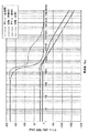
図7及び図8の周波数特性と図6の周波数特性を重ねることで、図9で示すようなスイッチングレギュレータ1のフィードバック系全体の周波数特性を得ることができる。なお、図9では、実線はスイッチングレギュレータ1の場合のゲインを、破線はスイッチングレギュレータ1の場合の位相を、1点鎖線は従来の電圧制御方式のスイッチングレギュレータの場合におけるゲインを、2点鎖線は従来の電圧制御方式のスイッチングレギュレータの場合における位相をそれぞれ示している。
図9から分かるように、図1のスイッチングレギュレータ1の場合は、高域周波数までゲインが伸びており、かつ位相余裕も確保されていることが分かる。これに対して、従来の電圧制御方式のスイッチングレギュレータでは、ゲインが伸びていないにも関わらず、すでに位相余裕がなく、安定性を求めるのであれば、更にゲインを下げて応答性能を低下させる必要がある。
The frequency characteristics of the entire feedback system of the
As can be seen from FIG. 9, in the case of the
なお、図1では降圧型のスイッチングレギュレータを例にして示したが、これは一例であり、本発明は、これに限定するものではなく昇圧型のスイッチングレギュレータにも適用することができ、この場合、図1は図10のようになる。
図10における図1との相違点は、図1のスイッチングトランジスタM1をNMOSトランジスタにし、図1の同期整流用トランジスタM2をPMOSトランジスタにして、スイッチングトランジスタM1、同期整流用トランジスタM2及びインダクタL1の接続を変えたことと、スイッチングトランジスタM1及び同期整流用トランジスタM2の各ゲートには、RSフリップフロップ回路7の非反転出力端Qから出力されたスイッチシグナル信号Sqが入力されるようにしたことである。
Although FIG. 1 shows an example of a step-down switching regulator, this is only an example, and the present invention is not limited to this and can be applied to a step-up switching regulator. FIG. 1 is as shown in FIG.
10 differs from FIG. 1 in that the switching transistor M1 in FIG. 1 is an NMOS transistor, the synchronous rectification transistor M2 in FIG. 1 is a PMOS transistor, and the switching transistor M1, the synchronous rectification transistor M2, and the inductor L1 are connected. And the switch signal signal Sq output from the non-inverting output terminal Q of the RS flip-flop circuit 7 is input to the gates of the switching transistor M1 and the synchronous rectification transistor M2. .
入力端子INと接地電圧との間には、インダクタL1とスイッチングトランジスタM1が直列に接続され、インダクタL1とスイッチングトランジスタM1との接続部である接続部Lxと出力端子OUTとの間に同期整流用トランジスタM2が接続されている。これ以外は図1と同じであり、各部の動作についても図1と同様であるのでその説明を省略する。
また、図1及び図10では、同期整流型のスイッチングレギュレータを例にして示したが、本発明は、非同期整流型のスイッチングレギュレータにも適用することができ、この場合、図1及び図10の同期整流用トランジスタM2を整流ダイオードに置き換えればよい。図1の場合、該整流ダイオードのアノードは接地電圧に接続され、カソードはスイッチングトランジスタM1のドレインに接続される。また、図10の場合は、整流ダイオードのアノードは接続部Lxに接続され、カソードは出力端子OUTに接続される。
An inductor L1 and a switching transistor M1 are connected in series between the input terminal IN and the ground voltage, and for synchronous rectification between a connection portion Lx, which is a connection portion between the inductor L1 and the switching transistor M1, and the output terminal OUT. Transistor M2 is connected. The rest is the same as in FIG. 1, and the operation of each part is the same as in FIG.
1 and 10 show a synchronous rectification type switching regulator as an example. However, the present invention can also be applied to an asynchronous rectification type switching regulator. In this case, as shown in FIG. The synchronous rectification transistor M2 may be replaced with a rectifier diode. In the case of FIG. 1, the anode of the rectifier diode is connected to the ground voltage, and the cathode is connected to the drain of the switching transistor M1. In the case of FIG. 10, the anode of the rectifier diode is connected to the connection portion Lx, and the cathode is connected to the output terminal OUT.
このように、本第1の実施の形態におけるスイッチングレギュレータは、スイッチングトランジスタM1のゲートに入力されるスイッチシグナル信号のデューティサイクルに応じて、誤差電圧Veとフィードバック電圧Vdfbとの電圧差を変えるようにしたことから、出力電圧Voutの変動に対する誤差電圧Veの変動の遅れを補償することができ、制御の安定性を向上させることができると共に周波数特性の改善を図ることができる。 As described above, the switching regulator according to the first embodiment changes the voltage difference between the error voltage Ve and the feedback voltage Vdfb according to the duty cycle of the switch signal signal input to the gate of the switching transistor M1. As a result, it is possible to compensate for a delay in fluctuation of the error voltage Ve with respect to fluctuations in the output voltage Vout, thereby improving control stability and improving frequency characteristics.
第2の実施の形態.
前記第1の実施の形態におけるフィードバック回路4において、スイッチシグナル信号Sqbに応じてフィードバック電圧Vdfbにスロープ電圧を加算するようにしてもよく、このようにしたものを本発明の第2の実施の形態とする。
図11は、本発明の第2の実施の形態におけるスイッチングレギュレータの回路例を示した図である。なお、図11では、図1と同じもの又は同様のものは同じ符号で示し、ここではその説明を省略する共に図1との相違点のみ説明する。
図11における図1との相違点は、図1のフィードバック回路4にスロープ加算回路を追加したことにあり、これに伴って、図1のフィードバック回路4をフィードバック回路4aに、図1のスイッチングレギュレータ1をスイッチングレギュレータ1aにした。
Second embodiment.
In the feedback circuit 4 in the first embodiment, a slope voltage may be added to the feedback voltage Vdfb in accordance with the switch signal signal Sqb, and such a configuration is used in the second embodiment of the present invention. And
FIG. 11 is a diagram illustrating a circuit example of the switching regulator according to the second embodiment of the present invention. In FIG. 11, the same or similar elements as those in FIG. 1 are denoted by the same reference numerals, and the description thereof will be omitted here, and only the differences from FIG.
11 is different from FIG. 1 in that a slope addition circuit is added to the feedback circuit 4 of FIG. 1, and accordingly, the feedback circuit 4 of FIG. 1 is replaced with the
図1のスイッチングレギュレータ1aは、入力端子INに入力された入力電圧Vinを所定の定電圧に降圧して出力電圧Voutとして出力端子OUTから出力する降圧型のスイッチングレギュレータをなしている。
スイッチングレギュレータ1aは、スイッチングトランジスタM1と、同期整流用トランジスタM2と、インダクタL1と、平滑用のコンデンサC1と、抵抗R1,R2と、位相補償用の抵抗R3及びコンデンサC2,C3と、基準電圧発生回路2と、誤差増幅回路3と、スイッチングトランジスタM1のゲートに入力されるパルス信号のデューティサイクルに応じたフィードバック電圧Vdfb1を生成して出力するフィードバック回路4aと、誤差増幅回路3からの誤差電圧Veとフィードバック電圧Vdfb1との電圧比較を行い、誤差電圧Veに応じたパルス幅を有するPWM制御を行うためのPWMパルス信号Spwmを生成して出力するPWMコンパレータ5と、発振回路6と、RSフリップフロップ回路7とを備えている。
The
The
図11のスイッチングレギュレータ1aの動作は、図1のフィードバック電圧Vdfbを、フィードバック電圧Vdfbにスロープ電圧を加算したフィードバック電圧Vdfb1にする以外は図1と同じであるのでその説明を省略する。
図12は、フィードバック回路4aの回路例を示した図であり、図13は、図12のフィードバック回路4aの動作例を示したタイミングチャートである。なお、図12では、図2と同じもの又は同様のものは同じ符号で示し、ここではその説明を省略すると共に図2との相違点のみ説明する。
Since the operation of the
FIG. 12 is a diagram illustrating a circuit example of the
図12における図2との相違点は、定電流源12、演算増幅回路13、PMOSトランジスタM13、NMOSトランジスタM14及びコンデンサC12を追加したことにある。
図12において、フィードバック回路4aは、PMOSトランジスタM11,M13、NMOSトランジスタM12,M14、定電流源11,12、演算増幅回路13、コンデンサC11,C12及び抵抗R11で構成されている。なお、定電流源12、演算増幅回路13、PMOSトランジスタM13、NMOSトランジスタM14及びコンデンサC12はスロープ電圧生成回路をなす。
12 differs from FIG. 2 in that a constant
In FIG. 12, the
入力電圧VinとPMOSトランジスタM13のソースとの間には定電流源12が接続され、PMOSトランジスタM13のソースには定電流源12から所定の定電流が供給されている。PMOSトランジスタM13のドレインと演算増幅回路13の出力端との間には、NMOSトランジスタM14とコンデンサC12が並列に接続されている。演算増幅回路13において、出力端は反転入力端に接続され、非反転入力端にはフィードバック電圧Vdfbが入力されている。PMOSトランジスタM13及びNMOSトランジスタM14の各ゲートは接続され、該接続部にはスイッチシグナル信号Sqbが入力され、PMOSトランジスタM13、NMOSトランジスタM14及びコンデンサC12の接続部からフィードバック電圧Vdfb1が出力される。
A constant
図2のフィードバック回路4では、定常点においてスイッチシグナル信号Sqbのデューティサイクルが50%を超えると、三角波をなすフィードバック電圧Vdfbのデューティサイクル変動に対するゲインが1を超えるため、動作が不安定になる。これは、電流制御方式のスイッチングレギュレータにおいてスロープ加算回路が必要であることと同様である。したがって、動作を安定化させるためには、ダウンスロープの1/2以上の傾きを持つスロープ電圧をアップスロープに加算する必要がある。定電流源12、演算増幅回路13、PMOSトランジスタM13、NMOSトランジスタM14及びコンデンサC12は、フィードバック電圧Vdfbのアップスロープにスロープ電圧を加算する回路を形成している。
In the feedback circuit 4 of FIG. 2, if the duty cycle of the switch signal signal Sqb exceeds 50% at a steady point, the gain with respect to the duty cycle fluctuation of the feedback voltage Vdfb forming the triangular wave exceeds 1, so that the operation becomes unstable. This is similar to the necessity of a slope addition circuit in a current control type switching regulator. Therefore, in order to stabilize the operation, it is necessary to add a slope voltage having a slope of 1/2 or more of the down slope to the up slope. The constant
演算増幅回路13によって、フィードバック電圧Vdfbをバーチャルショートし、コンデンサC12と定電流源12によってスロープ電圧を加算し、フィードバック電圧Vdfb1を生成している。スイッチシグナル信号Sqbがローレベルのときにスロープ電圧が加算され、スイッチシグナル信号Sqbがハイレベルのときには、フィードバック電圧Vdfb1はフィードバック電圧Vdfbに等しくなる。
The operational amplifier circuit 13 virtually shorts the feedback voltage Vdfb, and the slope voltage is added by the capacitor C12 and the constant
図13は、図12のフィードバック回路4aの動作例を示したタイミングチャートである。
図13において、フィードバック電圧Vdfbのダウンスロープは、本来であれば抵抗と容量との自由放電による関数になるが、説明を簡単にするために、直線で近似している。実線がフィードバック電圧Vdfbを示し、破線がフィードバック電圧Vdfbにダウンスロープの1/2の傾斜を持つスロープ電圧を加算したフィードバック電圧Vdfb1の波形を示している。
FIG. 13 is a timing chart showing an operation example of the
In FIG. 13, the downslope of the feedback voltage Vdfb is originally a function due to free discharge of resistance and capacity, but is approximated by a straight line for the sake of simplicity. The solid line indicates the feedback voltage Vdfb, and the broken line indicates the waveform of the feedback voltage Vdfb1 obtained by adding a slope voltage having a 1/2 slope of the downslope to the feedback voltage Vdfb.
フィードバック電圧Vdfb1において、アップスロープは、定電流源と容量によって一定の傾斜を有しているが、ダウンスロープは、抵抗と容量によって生成され、スイッチシグナル信号Sqbのデューティサイクルによって決まるフィードバック電圧Vdfbの定常点によって変動する。したがって、フィードバック電圧Vdfb1のダウンスロープは一定ではない。このことから、スイッチシグナル信号Sqbのデューティサイクルよって変わるダウンスロープの傾斜に合わせて、スロープ電圧の加算量を変動させるか、又はダウンスロープの傾斜が最も大きくなる状態に合わせてスロープ電圧の加算量を決定する必要がある。このことは、電流制御方式のスイッチングレギュレータにおけるスロープ補償回路においても同様である。 In the feedback voltage Vdfb1, the up slope has a constant slope depending on the constant current source and the capacity, but the down slope is generated by the resistance and the capacity, and the steady state of the feedback voltage Vdfb determined by the duty cycle of the switch signal signal Sqb. It varies depending on the point. Therefore, the down slope of the feedback voltage Vdfb1 is not constant. From this, the slope voltage addition amount is varied in accordance with the slope of the down slope that changes depending on the duty cycle of the switch signal signal Sqb, or the slope voltage addition amount is adjusted in accordance with the state in which the slope of the down slope becomes the largest. It is necessary to decide. The same applies to the slope compensation circuit in the current control switching regulator.
ここで、図12のフィードバック回路4aのように、変動するダウンスロープの傾斜に合わせてスロープ電圧の加算量を変動させるためには、更に制御回路が必要となる。また、ダウンスロープの傾斜が最も大きくなる状態に合わせてスロープ電圧の加算量を決定する場合には、フィードバック回路4aの微分特性が不必要に減少してしまう。そこで、このような問題に対応したフィードバック回路4aの回路例を図14に示す。
図14では、アップスロープを抵抗と容量で、ダウンスロープを定電流源と容量で作っているため、図12の場合とは逆にフィードバック電圧Vdfbのダウンスロープが一定の傾斜を有している。したがって、スロープ電圧の加算量は常に一定で良いため、前記のようなスロープ電圧の調整を行う必要がない。
Here, as in the
In FIG. 14, the up slope is made up of a resistor and a capacitor, and the down slope is made up of a constant current source and a capacitor. Therefore, contrary to the case of FIG. 12, the down slope of the feedback voltage Vdfb has a constant slope. Therefore, since the amount of addition of the slope voltage may be always constant, there is no need to adjust the slope voltage as described above.
なお、図11では降圧型のスイッチングレギュレータを例にして示したが、前記第1の実施の形態と同様、昇圧型のスイッチングレギュレータにも適用することができ、この場合、図10のフィードバック回路4をフィードバック回路4aに、図10のスイッチングレギュレータ1をスイッチングレギュレータ1aにすればよい。これ以外は図10と同様であるのでその説明を省略する。
また、前記説明では、同期整流型のスイッチングレギュレータを例にして示したが、本発明は、非同期整流型のスイッチングレギュレータにも適用することができ、この場合、前記第1の実施の形態と同様に、同期整流用トランジスタM2を整流ダイオードに置き換えればよい。
11 shows a step-down switching regulator as an example, but the present invention can also be applied to a step-up switching regulator as in the first embodiment. In this case, the feedback circuit 4 in FIG. May be used as the
In the above description, the synchronous rectification type switching regulator is shown as an example. However, the present invention can also be applied to an asynchronous rectification type switching regulator. In this case, the same as in the first embodiment. In addition, the synchronous rectification transistor M2 may be replaced with a rectifier diode.
このように、本第2の実施の形態におけるスイッチングレギュレータは、前記第1の実施の形態におけるフィードバック回路4において、スイッチシグナル信号Sqbに応じてフィードバック電圧Vdfbにスロープ電圧を加算するようにしたことから、前記第1の実施の形態と同様の効果を得ることができると共に、フィードバック回路の動作を更に安定させることができ、制御の安定性を更に向上させることができる。 As described above, the switching regulator according to the second embodiment adds the slope voltage to the feedback voltage Vdfb in accordance with the switch signal signal Sqb in the feedback circuit 4 according to the first embodiment. The effects similar to those of the first embodiment can be obtained, the operation of the feedback circuit can be further stabilized, and the control stability can be further improved.
1,1a スイッチングレギュレータ
2 基準電圧発生回路
3 誤差増幅回路
4,4a フィードバック回路
5 PWMコンパレータ
6 発振回路
7 RSフリップフロップ回路
M1 スイッチングトランジスタ
M2 同期整流用トランジスタ
L1 インダクタ
C1〜C3 コンデンサ
R1〜R3 抵抗
DESCRIPTION OF
Claims (14)
入力された制御信号に応じてスイッチングを行うスイッチング素子と、
該スイッチング素子のスイッチングによって前記電源電圧による充電が行われるインダクタと、
前記スイッチング素子がオフして該インダクタへの充電が停止すると、該インダクタの放電を行う整流素子と、
前記出力電圧に比例した比例電圧と所定の基準電圧との電圧差に応じた誤差電圧を生成し、該誤差電圧に応じたデューティサイクルのパルス信号を生成して前記スイッチング素子の制御電極に出力し前記スイッチング素子のスイッチング制御を行う制御回路部と、
を備え、
前記制御回路部は、前記パルス信号のデューティサイクルに基づいてフィードバック電圧を生成し、該生成したフィードバック電圧と前記誤差電圧との電圧差に応じたデューティサイクルの前記パルス信号を生成し、該電圧差を前記パルス信号のデューティサイクルに応じて可変するフィードバック制御を行うことを特徴とするスイッチングレギュレータ。 In the switching regulator that converts the power supply voltage input to the input terminal to a predetermined constant voltage and outputs it as an output voltage from the output terminal.
A switching element that performs switching according to the input control signal;
An inductor charged by the power supply voltage by switching of the switching element;
When the switching element is turned off and charging to the inductor is stopped, the rectifying element for discharging the inductor;
An error voltage corresponding to a voltage difference between a proportional voltage proportional to the output voltage and a predetermined reference voltage is generated, and a pulse signal having a duty cycle corresponding to the error voltage is generated and output to the control electrode of the switching element. A control circuit unit that performs switching control of the switching element;
With
The control circuit unit generates a feedback voltage based on a duty cycle of the pulse signal, generates the pulse signal having a duty cycle corresponding to a voltage difference between the generated feedback voltage and the error voltage, and the voltage difference A switching regulator characterized in that feedback control is performed to vary the frequency according to the duty cycle of the pulse signal.
前記出力電圧に比例した比例電圧と所定の基準電圧との電圧差に応じた誤差電圧を生成して出力する誤差電圧生成回路部と、
前記誤差電圧に応じたデューティサイクルのパルス信号を生成して前記スイッチング素子の制御電極に出力し該スイッチング素子のスイッチング制御を行うパルス変調回路部と、
前記パルス信号のデューティサイクルに応じたフィードバック電圧を生成して出力するフィードバック回路部と、
を備え、
前記パルス変調回路部は、前記誤差電圧と前記フィードバック電圧との電圧比較を行い、該比較結果に応じたデューティサイクルの前記パルス信号を生成することを特徴とする請求項2記載のスイッチングレギュレータ。 The control circuit unit is
An error voltage generation circuit unit that generates and outputs an error voltage corresponding to a voltage difference between a proportional voltage proportional to the output voltage and a predetermined reference voltage;
A pulse modulation circuit unit that generates a pulse signal having a duty cycle according to the error voltage and outputs the pulse signal to a control electrode of the switching element to perform switching control of the switching element;
A feedback circuit unit that generates and outputs a feedback voltage according to a duty cycle of the pulse signal;
With
The switching regulator according to claim 2, wherein the pulse modulation circuit unit compares the error voltage with the feedback voltage and generates the pulse signal having a duty cycle corresponding to the comparison result.
前記パルス信号に応じてスイッチングを行う第1スイッチと、
前記パルス信号に応じて該第1スイッチと相反するスイッチングを行う第2スイッチと、
コンデンサと、
前記第1スイッチのスイッチングに応じて所定の定電流を該コンデンサに供給して充電を行う定電流源と、
前記第2スイッチのスイッチングに応じて前記コンデンサを放電する際に所定の時定数を形成する抵抗と、
を備えることを特徴とする請求項4記載のスイッチングレギュレータ。 The feedback circuit unit includes:
A first switch that performs switching in response to the pulse signal;
A second switch that performs switching opposite to the first switch in response to the pulse signal;
A capacitor,
A constant current source for charging the capacitor by supplying a predetermined constant current in response to switching of the first switch;
A resistor that forms a predetermined time constant when discharging the capacitor in response to switching of the second switch;
The switching regulator according to claim 4, further comprising:
前記パルス信号に応じてスイッチングを行う第1スイッチと、
前記パルス信号に応じて該第1スイッチと相反するスイッチングを行う第2スイッチと、
コンデンサと、
前記第1スイッチのスイッチングに応じて所定の定電流を該コンデンサに供給して充電を行う定電流源と、
前記第2スイッチのスイッチングに応じて前記コンデンサを放電する際に所定の時定数を形成する抵抗と、
前記スロープ電圧を生成して、前記コンデンサの充放電端の充電時における電圧に、該生成したスロープ電圧を加算して前記フィードバック電圧を生成するスロープ電圧生成回路と、
を備えることを特徴とする請求項6記載のスイッチングレギュレータ。 The feedback circuit unit includes:
A first switch that performs switching in response to the pulse signal;
A second switch that performs switching opposite to the first switch in response to the pulse signal;
A capacitor,
A constant current source for charging the capacitor by supplying a predetermined constant current in response to switching of the first switch;
A resistor that forms a predetermined time constant when discharging the capacitor in response to switching of the second switch;
A slope voltage generation circuit that generates the slope voltage and adds the generated slope voltage to the voltage at the time of charging of the charge / discharge end of the capacitor to generate the feedback voltage;
The switching regulator according to claim 6, further comprising:
前記パルス信号に応じてスイッチングを行う第1スイッチと、
前記パルス信号に応じて該第1スイッチと相反するスイッチングを行う第2スイッチと、
抵抗と
前記第1スイッチのスイッチングに応じて、該抵抗を介して電流が供給されて充電されるコンデンサと、
前記第2スイッチのスイッチングに応じて、該コンデンサの放電を行う定電流源と、
前記スロープ電圧を生成して、前記コンデンサの充放電端の充電時における電圧に、該生成したスロープ電圧を加算して前記フィードバック電圧を生成するスロープ電圧生成回路と、
を備えることを特徴とする請求項6記載のスイッチングレギュレータ。 The feedback circuit unit includes:
A first switch that performs switching in response to the pulse signal;
A second switch that performs switching opposite to the first switch in response to the pulse signal;
A resistor and a capacitor charged with a current supplied through the resistor in response to switching of the first switch;
A constant current source for discharging the capacitor in response to switching of the second switch;
A slope voltage generation circuit that generates the slope voltage and adds the generated slope voltage to the voltage at the time of charging of the charge / discharge end of the capacitor to generate the feedback voltage;
The switching regulator according to claim 6, further comprising:
前記出力電圧を分圧して前記比例電圧を生成し出力する出力電圧検出回路と、
前記基準電圧を生成して出力する基準電圧発生回路と、
前記比例電圧と前記基準電圧との電圧差を増幅して前記誤差電圧を生成し出力する誤差増幅回路と、
を備えることを特徴とする請求項3、4、5、6、7又は8記載のスイッチングレギュレータ。 The error voltage generation circuit unit includes:
An output voltage detection circuit that divides the output voltage to generate and output the proportional voltage;
A reference voltage generating circuit for generating and outputting the reference voltage;
An error amplifying circuit for amplifying a voltage difference between the proportional voltage and the reference voltage to generate and output the error voltage;
The switching regulator according to claim 3, 4, 5, 6, 7 or 8.
前記誤差電圧と前記フィードバック電圧との電圧比較を行い、該電圧比較結果を示す2値の信号を生成して出力する電圧比較回路と、
一方の入力端に所定のクロック信号が入力されると共に他方の入力端に該電圧比較回路の出力信号が入力され、該出力信号と前記クロック信号の各信号レベルに応じた前記パルス信号を生成し出力するRSフリップフロップ回路と、
を備えることを特徴とする請求項3、4、5、6、7、8又は9記載のスイッチングレギュレータ。 The pulse modulation circuit section is
A voltage comparison circuit that performs a voltage comparison between the error voltage and the feedback voltage, and generates and outputs a binary signal indicating the voltage comparison result;
A predetermined clock signal is input to one input terminal and the output signal of the voltage comparison circuit is input to the other input terminal, and the pulse signal corresponding to each signal level of the output signal and the clock signal is generated. An output RS flip-flop circuit;
The switching regulator according to claim 3, 4, 5, 6, 7, 8, or 9.
該スイッチング素子のスイッチングによって、入力端子に入力された入力電圧による充電が行われるインダクタと、
前記スイッチング素子がオフして該インダクタへの充電が停止すると、該インダクタの放電を行う整流素子と、
を備え、
出力端子から出力される出力電圧に比例した比例電圧と所定の基準電圧との電圧差に応じた誤差電圧を生成し、該誤差電圧に応じたデューティサイクルのパルス信号を生成して前記スイッチング素子の制御電極に出力し該スイッチング素子のスイッチング制御を行い、前記入力端子に入力された入力電圧を所定の定電圧に変換して前記出力電圧として出力するスイッチングレギュレータの動作制御方法において、
前記パルス信号のデューティサイクルに基づいてフィードバック電圧を生成し、
該生成したフィードバック電圧と前記誤差電圧との電圧差に応じたデューティサイクルの前記パルス信号を生成し、
該電圧差を前記パルス信号のデューティサイクルに応じて可変するフィードバック制御を行うことを特徴とするスイッチングレギュレータの動作制御方法。 A switching element that performs switching according to the input control signal;
An inductor that is charged by the input voltage input to the input terminal by switching of the switching element;
When the switching element is turned off and charging to the inductor is stopped, the rectifying element for discharging the inductor;
With
An error voltage corresponding to a voltage difference between a proportional voltage proportional to the output voltage output from the output terminal and a predetermined reference voltage is generated, and a pulse signal having a duty cycle corresponding to the error voltage is generated to In the operation control method of the switching regulator that outputs to the control electrode, performs switching control of the switching element, converts the input voltage input to the input terminal into a predetermined constant voltage, and outputs the voltage as the output voltage.
Generating a feedback voltage based on the duty cycle of the pulse signal;
Generating the pulse signal with a duty cycle according to a voltage difference between the generated feedback voltage and the error voltage;
An operation control method for a switching regulator, wherein feedback control is performed to vary the voltage difference according to a duty cycle of the pulse signal.
Priority Applications (6)
| Application Number | Priority Date | Filing Date | Title |
|---|---|---|---|
| JP2007195865A JP5386801B2 (en) | 2007-07-27 | 2007-07-27 | Switching regulator and operation control method thereof |
| KR1020097005746A KR101055339B1 (en) | 2007-07-27 | 2008-06-17 | Switching regulator and its operation control method |
| CN2008800007959A CN101548456B (en) | 2007-07-27 | 2008-06-17 | Switching regulator and method for controlling operation thereof |
| PCT/JP2008/061389 WO2009016898A1 (en) | 2007-07-27 | 2008-06-17 | Switching regulator and method for controlling operation thereof |
| US12/439,789 US8207721B2 (en) | 2007-07-27 | 2008-06-17 | Switching regulator capable of stable operation and improved frequency characteristics in a broad input and output voltage range and method for controlling operation thereof |
| TW097125104A TWI405062B (en) | 2007-07-27 | 2008-07-03 | Switching regulator and method for controlling operation thereof |
Applications Claiming Priority (1)
| Application Number | Priority Date | Filing Date | Title |
|---|---|---|---|
| JP2007195865A JP5386801B2 (en) | 2007-07-27 | 2007-07-27 | Switching regulator and operation control method thereof |
Publications (2)
| Publication Number | Publication Date |
|---|---|
| JP2009033883A JP2009033883A (en) | 2009-02-12 |
| JP5386801B2 true JP5386801B2 (en) | 2014-01-15 |
Family
ID=40304135
Family Applications (1)
| Application Number | Title | Priority Date | Filing Date |
|---|---|---|---|
| JP2007195865A Active JP5386801B2 (en) | 2007-07-27 | 2007-07-27 | Switching regulator and operation control method thereof |
Country Status (6)
| Country | Link |
|---|---|
| US (1) | US8207721B2 (en) |
| JP (1) | JP5386801B2 (en) |
| KR (1) | KR101055339B1 (en) |
| CN (1) | CN101548456B (en) |
| TW (1) | TWI405062B (en) |
| WO (1) | WO2009016898A1 (en) |
Families Citing this family (48)
| Publication number | Priority date | Publication date | Assignee | Title |
|---|---|---|---|---|
| JP5309683B2 (en) | 2008-05-13 | 2013-10-09 | 株式会社リコー | Step-down switching regulator |
| JP5063474B2 (en) | 2008-05-13 | 2012-10-31 | 株式会社リコー | Current mode control switching regulator and operation control method thereof |
| JP5381195B2 (en) * | 2009-03-17 | 2014-01-08 | 株式会社リコー | Semiconductor device and operation control method thereof |
| TWI396375B (en) | 2009-09-18 | 2013-05-11 | Leadtrend Tech Corp | Switching power supply and related control method |
| JP5298050B2 (en) | 2010-03-11 | 2013-09-25 | トヨタ自動車株式会社 | Switching power supply circuit |
| CN102314187B (en) * | 2010-06-30 | 2014-01-01 | 比亚迪股份有限公司 | Direct-current voltage proportion output circuit and control method thereof |
| TWI411901B (en) * | 2010-08-23 | 2013-10-11 | Anpec Electronics Corp | Switching regulator |
| CN101951158B (en) * | 2010-09-14 | 2013-04-03 | Bcd半导体制造有限公司 | Compensating controller of PWM converter and PWM control circuit |
| TW201224694A (en) * | 2010-12-06 | 2012-06-16 | Eneraiser Technology Co Ltd | Phase-controlled alternative current voltage regulator circuit |
| JP2012130137A (en) * | 2010-12-14 | 2012-07-05 | On Semiconductor Trading Ltd | Switching control circuit |
| JP5798328B2 (en) * | 2011-02-01 | 2015-10-21 | セイコーインスツル株式会社 | Switching regulator control circuit and switching regulator |
| JP5768475B2 (en) * | 2011-04-28 | 2015-08-26 | ミツミ電機株式会社 | Switching power supply |
| JP5944113B2 (en) | 2011-05-27 | 2016-07-05 | リコー電子デバイス株式会社 | Switching regulator control circuit and method, and switching regulator |
| JP5902401B2 (en) | 2011-05-31 | 2016-04-13 | サイプレス セミコンダクター コーポレーション | Power supply device, control circuit, electronic device, and power supply control method |
| WO2013009122A2 (en) * | 2011-07-14 | 2013-01-17 | (주)제퍼로직 | Switching mode power supply apparatus comprising tilt compensation circuit |
| JP2013046496A (en) * | 2011-08-24 | 2013-03-04 | Fujitsu Semiconductor Ltd | Control circuit, power supply device, and method of controlling power supply |
| JP5366029B2 (en) * | 2011-09-22 | 2013-12-11 | Tdk株式会社 | Power supply device and light emitting element driving device |
| JP5875073B2 (en) * | 2012-01-20 | 2016-03-02 | 国立大学法人 大分大学 | Switching power supply device and pulse width modulation circuit used in the device |
| JP2013165537A (en) * | 2012-02-09 | 2013-08-22 | Ricoh Co Ltd | Switching regulator, control method thereof, and power supply device |
| JP6039327B2 (en) | 2012-09-14 | 2016-12-07 | リコー電子デバイス株式会社 | Switching power supply |
| TWI457741B (en) * | 2012-09-18 | 2014-10-21 | Upi Semiconductor Corp | Dc-dc controller |
| KR101985934B1 (en) * | 2012-11-23 | 2019-06-05 | 엘지디스플레이 주식회사 | DC-DC Converter Controlled by Pulse Width Modulation Manner |
| US9337731B2 (en) * | 2012-12-13 | 2016-05-10 | Linear Technology Corporation | Power converter for generating both positive and negative output signals |
| JP6153732B2 (en) * | 2013-01-21 | 2017-06-28 | リコー電子デバイス株式会社 | Switching regulator |
| JP5834039B2 (en) * | 2013-03-13 | 2015-12-16 | 株式会社東芝 | Step-down switching circuit |
| TWI496389B (en) | 2013-05-16 | 2015-08-11 | Upi Semiconductor Corp | Timing generator and timing signal generation method for power converter |
| TW201445858A (en) | 2013-05-16 | 2014-12-01 | Upi Semiconductor Corp | Timing generator and timing signal generation method for power converter |
| TWI497882B (en) * | 2013-05-17 | 2015-08-21 | Upi Semiconductor Corp | Power converter and operating method thereof |
| US9504103B2 (en) * | 2013-10-21 | 2016-11-22 | Osram Sylvania Inc. | Driving a multi-color luminaire |
| TWI555317B (en) * | 2013-11-27 | 2016-10-21 | 力智電子股份有限公司 | Power converter and slope detection controller and method thereof |
| CN103683935A (en) * | 2013-12-03 | 2014-03-26 | 成都芯源系统有限公司 | Switch mode power supply and control circuit and control method thereof |
| KR101509752B1 (en) * | 2013-12-23 | 2015-04-07 | 현대자동차 주식회사 | Apparatus and method for charging the battery of vehicle |
| EP2919374B1 (en) * | 2014-03-12 | 2018-05-02 | DET International Holding Limited | Duty-ratio controller |
| US9698683B2 (en) * | 2014-07-11 | 2017-07-04 | Infineon Technologies Austria Ag | Method and apparatus for controller optimization of a switching voltage regulator |
| US9501073B2 (en) | 2015-01-12 | 2016-11-22 | Huawei Technologies Co., Ltd. | Low-noise sampled voltage regulator |
| FR3047815B1 (en) * | 2016-02-11 | 2018-03-09 | STMicroelectronics (Alps) SAS | DEVICE FOR CONTROLLING A CURRENT IN AN UNKNOWN CURRENT-VOLTAGE CHARACTERISTIC CHARGE |
| CA3005717C (en) | 2016-02-17 | 2021-06-22 | Halliburton Energy Services, Inc. | Wide-input-range downhole power supply |
| JP6594797B2 (en) * | 2016-02-26 | 2019-10-23 | エイブリック株式会社 | Switching regulator |
| CN105896979B (en) * | 2016-04-13 | 2018-10-16 | 上海晶丰明源半导体股份有限公司 | A kind of analog regulation reference circuit and its Switching Power Supply |
| US10050517B1 (en) | 2017-01-31 | 2018-08-14 | Ricoh Electronics Devices Co., Ltd. | Power supply apparatus converting input voltage to predetermined output voltage and controlling output voltage based on feedback signal corresponding to output voltage |
| US10063143B1 (en) * | 2017-02-24 | 2018-08-28 | Texas Instruments Incorporated | Fixed frequency DC-DC converter |
| WO2018211980A1 (en) * | 2017-05-17 | 2018-11-22 | ソニーセミコンダクタソリューションズ株式会社 | Power supply circuit and power supply device |
| CN109240406A (en) * | 2018-11-29 | 2019-01-18 | 浙江亿邦通信科技有限公司 | A kind of voltage follower circuit for ore machine apparatus |
| CN112202373B (en) * | 2019-07-01 | 2022-05-06 | 北京小米移动软件有限公司 | Electronic device |
| TW202144804A (en) * | 2020-05-22 | 2021-12-01 | 茂達電子股份有限公司 | Inductor current detecting circuit |
| TWI746099B (en) * | 2020-08-03 | 2021-11-11 | 茂達電子股份有限公司 | Converter having fast transient response |
| CN114094824B (en) * | 2021-11-24 | 2024-08-30 | 深圳市纳芯威科技有限公司 | Switching power supply circuit and control method |
| CN114465449A (en) * | 2021-12-28 | 2022-05-10 | 中国电子科技集团公司第二十九研究所 | Circuit for regulating gain stability of switching power supply |
Family Cites Families (24)
| Publication number | Priority date | Publication date | Assignee | Title |
|---|---|---|---|---|
| US5029269A (en) * | 1990-04-12 | 1991-07-02 | Rockwell International Corporation | Delayed power supply overvoltage shutdown apparatus |
| US5770940A (en) * | 1995-08-09 | 1998-06-23 | Switch Power, Inc. | Switching regulator |
| DE19713814A1 (en) * | 1997-04-03 | 1998-10-15 | Siemens Ag | Switching power supply |
| US5903452A (en) * | 1997-08-11 | 1999-05-11 | System General Corporation | Adaptive slope compensator for current mode power converters |
| JP4389379B2 (en) * | 2000-11-27 | 2009-12-24 | 株式会社デンソー | Dual battery mounted vehicle power supply |
| US6545882B2 (en) * | 2001-08-15 | 2003-04-08 | System General Corp. | PWM controller having off-time modulation for power converter |
| JP4110926B2 (en) * | 2002-07-11 | 2008-07-02 | 富士電機デバイステクノロジー株式会社 | DC-DC converter |
| JP4259119B2 (en) * | 2003-01-21 | 2009-04-30 | 株式会社豊田自動織機 | Output power detection circuit and switching power supply device with output current detection function |
| TW595076B (en) * | 2003-05-19 | 2004-06-21 | Richtek Technology Corp | Delta-sigma DC to DC converter and its method |
| CN100431249C (en) * | 2003-08-28 | 2008-11-05 | 立锜科技股份有限公司 | Difference sum dc-dc converter and method thereof |
| JP4387170B2 (en) * | 2003-11-27 | 2009-12-16 | 株式会社リコー | Switching regulator |
| JP4498006B2 (en) * | 2004-05-12 | 2010-07-07 | セイコーインスツル株式会社 | Switching regulator control circuit and switching regulator |
| JP2006033958A (en) | 2004-07-14 | 2006-02-02 | Seiko Instruments Inc | Switching regulator |
| CN100508338C (en) * | 2004-10-28 | 2009-07-01 | Tdk株式会社 | Switching power supply control device and switching power supply |
| JP2006166667A (en) * | 2004-12-10 | 2006-06-22 | Ricoh Co Ltd | Switching regulator |
| US7453250B2 (en) * | 2005-02-10 | 2008-11-18 | Intersil Americas Inc. | PWM controller with dual-edge modulation using dual ramps |
| CN100466434C (en) * | 2005-02-10 | 2009-03-04 | 英特赛尔美国股份有限公司 | Pwm controller with dual-edge modulation using dual ramps |
| JP4619822B2 (en) | 2005-03-03 | 2011-01-26 | 株式会社リコー | Switching regulator and voltage control method thereof |
| TWI291801B (en) * | 2005-10-13 | 2007-12-21 | System General Corp | High efficiency buck converter |
| US7378826B2 (en) * | 2006-01-05 | 2008-05-27 | Linear Technology Corp. | Methods and circuits for output over-voltage reduction in switching regulators |
| JP4671354B2 (en) | 2006-03-15 | 2011-04-13 | 株式会社リコー | Image compression apparatus and image compression method |
| JP4836624B2 (en) | 2006-03-23 | 2011-12-14 | 株式会社リコー | Switching regulator |
| US7646185B2 (en) * | 2006-08-25 | 2010-01-12 | Micrel, Inc. | Automatic external switch detection in synchronous switching regulator controller |
| TW200814533A (en) * | 2006-09-11 | 2008-03-16 | Beyond Innovation Tech Co Ltd | Apparatus for pulse width modulation and circuit and method for controlling thereof |
-
2007
- 2007-07-27 JP JP2007195865A patent/JP5386801B2/en active Active
-
2008
- 2008-06-17 KR KR1020097005746A patent/KR101055339B1/en active IP Right Grant
- 2008-06-17 US US12/439,789 patent/US8207721B2/en active Active
- 2008-06-17 WO PCT/JP2008/061389 patent/WO2009016898A1/en active Application Filing
- 2008-06-17 CN CN2008800007959A patent/CN101548456B/en active Active
- 2008-07-03 TW TW097125104A patent/TWI405062B/en active
Also Published As
| Publication number | Publication date |
|---|---|
| KR20090048638A (en) | 2009-05-14 |
| US8207721B2 (en) | 2012-06-26 |
| CN101548456A (en) | 2009-09-30 |
| US20100181977A1 (en) | 2010-07-22 |
| TWI405062B (en) | 2013-08-11 |
| TW200921317A (en) | 2009-05-16 |
| KR101055339B1 (en) | 2011-08-09 |
| JP2009033883A (en) | 2009-02-12 |
| CN101548456B (en) | 2012-07-11 |
| WO2009016898A1 (en) | 2009-02-05 |
Similar Documents
| Publication | Publication Date | Title |
|---|---|---|
| JP5386801B2 (en) | Switching regulator and operation control method thereof | |
| JP5014772B2 (en) | Current mode control switching regulator | |
| JP5063474B2 (en) | Current mode control switching regulator and operation control method thereof | |
| JP4725641B2 (en) | Buck-boost switching regulator | |
| Huang et al. | Hybrid buck–boost feedforward and reduced average inductor current techniques in fast line transient and high-efficiency buck–boost converter | |
| US11381167B2 (en) | Power converter with slope compensation | |
| JP5195182B2 (en) | Current mode control switching regulator | |
| TWI479787B (en) | Method and apparatus for controlling a conversion of power, and switching regulator | |
| US7208928B2 (en) | Oscillatorless DC-DC power converter | |
| US7199563B2 (en) | DC-DC converter | |
| US8587265B2 (en) | Control circuit for DC-DC converter, DC-DC converter, and method for controlling DC-DC converter | |
| JP5852380B2 (en) | DC / DC converter | |
| JP2010011576A (en) | Switching regulator | |
| US9520777B2 (en) | Time signal generator and time signal generating method | |
| JP2009153289A (en) | Dc-dc converter | |
| KR101742760B1 (en) | Dc-dc converter | |
| JP2020065402A (en) | Switching regulator | |
| JP6160188B2 (en) | Switching regulator | |
| TW201445858A (en) | Timing generator and timing signal generation method for power converter | |
| JP6153732B2 (en) | Switching regulator | |
| JP2012016123A (en) | Dc-dc converter | |
| CN116915047A (en) | DC-DC converter circuit and corresponding method of operation | |
| JP6912300B2 (en) | Switching regulator | |
| JP2010063290A (en) | Power supply control circuit | |
| CN114726209A (en) | Feedback circuit with adjustable loop gain for boost converter |
Legal Events
| Date | Code | Title | Description |
|---|---|---|---|
| A621 | Written request for application examination |
Free format text: JAPANESE INTERMEDIATE CODE: A621 Effective date: 20100222 |
|
| A131 | Notification of reasons for refusal |
Free format text: JAPANESE INTERMEDIATE CODE: A131 Effective date: 20120508 |
|
| A521 | Request for written amendment filed |
Free format text: JAPANESE INTERMEDIATE CODE: A523 Effective date: 20120703 |
|
| A131 | Notification of reasons for refusal |
Free format text: JAPANESE INTERMEDIATE CODE: A131 Effective date: 20130129 |
|
| TRDD | Decision of grant or rejection written | ||
| A01 | Written decision to grant a patent or to grant a registration (utility model) |
Free format text: JAPANESE INTERMEDIATE CODE: A01 Effective date: 20130910 |
|
| A61 | First payment of annual fees (during grant procedure) |
Free format text: JAPANESE INTERMEDIATE CODE: A61 Effective date: 20130923 |
|
| R151 | Written notification of patent or utility model registration |
Ref document number: 5386801 Country of ref document: JP Free format text: JAPANESE INTERMEDIATE CODE: R151 |
|
| S111 | Request for change of ownership or part of ownership |
Free format text: JAPANESE INTERMEDIATE CODE: R313111 |
|
| R350 | Written notification of registration of transfer |
Free format text: JAPANESE INTERMEDIATE CODE: R350 |
|
| R250 | Receipt of annual fees |
Free format text: JAPANESE INTERMEDIATE CODE: R250 |
|
| R250 | Receipt of annual fees |
Free format text: JAPANESE INTERMEDIATE CODE: R250 |
|
| R250 | Receipt of annual fees |
Free format text: JAPANESE INTERMEDIATE CODE: R250 |
|
| R250 | Receipt of annual fees |
Free format text: JAPANESE INTERMEDIATE CODE: R250 |
|
| R250 | Receipt of annual fees |
Free format text: JAPANESE INTERMEDIATE CODE: R250 |
|
| R250 | Receipt of annual fees |
Free format text: JAPANESE INTERMEDIATE CODE: R250 |
|
| S111 | Request for change of ownership or part of ownership |
Free format text: JAPANESE INTERMEDIATE CODE: R313111 |
|
| R350 | Written notification of registration of transfer |
Free format text: JAPANESE INTERMEDIATE CODE: R350 |
|
| R250 | Receipt of annual fees |
Free format text: JAPANESE INTERMEDIATE CODE: R250 |
|
| R250 | Receipt of annual fees |
Free format text: JAPANESE INTERMEDIATE CODE: R250 |