JP2006033958A - Switching regulator - Google Patents
Switching regulator Download PDFInfo
- Publication number
- JP2006033958A JP2006033958A JP2004207224A JP2004207224A JP2006033958A JP 2006033958 A JP2006033958 A JP 2006033958A JP 2004207224 A JP2004207224 A JP 2004207224A JP 2004207224 A JP2004207224 A JP 2004207224A JP 2006033958 A JP2006033958 A JP 2006033958A
- Authority
- JP
- Japan
- Prior art keywords
- slope compensation
- vout
- switching regulator
- slope
- input
- Prior art date
- Legal status (The legal status is an assumption and is not a legal conclusion. Google has not performed a legal analysis and makes no representation as to the accuracy of the status listed.)
- Withdrawn
Links
Images


Abstract
Description
この発明は、入力電圧および出力電圧に応じてスロープ補償の量を変化させる電流モードスイッチングレギュレータに関するものである。 The present invention relates to a current mode switching regulator that changes the amount of slope compensation in accordance with an input voltage and an output voltage.
従来の電流モード昇圧型スイッチングレギュレータとしては、図4のブロック図に示されるような回路が知られている。 As a conventional current mode step-up switching regulator, a circuit as shown in the block diagram of FIG. 4 is known.
スイッチ107がオンすることにより入力電圧VINがコイル108に蓄積され、スイッチ107がオフすることでコイル108に蓄積されたエネルギーがダイオード109を介して出力コンデンサ112に転送される。
When the
エラーアンプ101は、出力電圧VOUTを帰還抵抗である抵抗110と抵抗111で分圧した電圧と、基準電圧源100から供給される基準電圧VREFとの差を増幅する。スロープ補償回路102は発振器104の出力信号に同期したこぎり波状の補償ランプ波を発生し、加算器103の一方の入力端子に入力される。
The
加算器103の他方の入力端子にはスイッチ107に流れる電流の情報、あるいはコイル108に流れる電流の情報を電圧に変換したものが入力される。通常はスイッチ107あるいはコイル108と直列に接続したセンス抵抗を用いて各素子に流れる電流を検出し、スイッチ107あるいはコイル108に流れる電流に比例した値が電圧情報として加算器103の入力端子に入力される。
Information on the current flowing through the
コンパレータ105の反転入力端子にはエラーアンプ101の出力信号が入力され、非反転入力端子には加算器103の出力信号が入力される。出力電圧VOUTが低いと、エラーアンプ101の出力は上昇するので、コンパレータ105の状態がLからHに遷移するには、より大きな値をコンパレータ105の非反転入力端子に印加する必要がある。すなわち出力電圧VOUTが低いと、スイッチ107あるいはコイル108により多くの電流を流すことでコンパレータ105の出力が反転する。コンパレータ105の出力はSR−ラッチ106のリセット端子Rに入力される。
The output signal of the
SR−ラッチ106のセット端子Sには発振器104が接続されており、発振器104からは図中に示したように一定周期のパルスが出力されている。SR−ラッチ106の出力端子Qはスイッチ107に接続されており、SR−ラッチ106の出力端子QがHのとき、スイッチ107がONする(例えば、特許文献1参照)。
電流モードスイッチングレギュレータでは、“ピーク電流制御型DC−DCコンバータの特性”、電子通信学会論文誌‘86/4 Vol.J69−C No.4 pp487−494で原田耕介らが指摘しているようにクロックサイクルに対してインダクタ電流が上昇する期間の割合、すなわちデューティーが50%を越える場合、電流モードスイッチングレギュレータはデューティーが周期的に変化する不安定状態(サブハーモニック発振状態)になる。 In the current mode switching regulator, “Characteristics of DC-DC Converter with Peak Current Control”, IEICE Transactions '86 / 4 Vol. J69-C No. As indicated by Kosuke Harada et al. In 4 pp 487-494, the ratio of the period during which the inductor current rises with respect to the clock cycle, that is, when the duty exceeds 50%, the duty of the current mode switching regulator changes periodically. It becomes unstable (sub harmonic oscillation state).
さらに、サブハーモニック発振を防止するためにはコイル電流の上昇率および減少率に対して、適切な量のスロープ補償を行う必要があることを原田らは指摘している。図3の電流モード昇圧型スイッチングレギュレータにおいてサブハーモニック発振を防止するために必要なスロープ補償値を求める。 Furthermore, Harada et al. Point out that in order to prevent subharmonic oscillation, it is necessary to perform an appropriate amount of slope compensation for the rate of increase and decrease of the coil current. In the current mode step-up switching regulator of FIG. 3, a slope compensation value necessary for preventing subharmonic oscillation is obtained.
すなわち、スイッチ107がONしているときのコイル108の電流増加率m1はコイル108のインダクタンスをL、スイッチングレギュレータの入力電圧をVINとすると
m1=VIN/L ・・・(1)
となりスイッチ107がOFFしている時のコイル108の電流減少率m2はダイオード109による電圧降下を無視するとおよそ
m2=(VOUT−VIN)/L ・・・(2)
となる。
That is, when the
When the
It becomes.
(1)式(2)式より入力電圧VIN、出力電圧VOUTにおけるサブハーモニック発振を防止するために必要なスロープ補償値mは
m≧(m2−m1)/2=(VOUT−2VIN)/(2L) ・・・(3)
となる。
(1) From equation (2), the slope compensation value m required to prevent subharmonic oscillation at the input voltage VIN and output voltage VOUT is m ≧ (m2−m1) / 2 = (VOUT−2VIN) / (2L (3)
It becomes.
しかし、図3の従来の電流モード昇圧型スイッチングレギュレータでは、スロープ補償回路から出力されるスロープ補償の量である補償ランプ波の増加率は一定のため、通常、考えられる入力電圧VINおよび出力電圧VOUT範囲で最大のスロープ補償値に設定する必要がある。しかしこの場合、スロープ補償値は通常大きな値となり、大きなスロープ補償値により電流モードによるスイッチングレギュレータの特性が損なわれるという問題点があった。 However, in the conventional current mode step-up switching regulator shown in FIG. 3, since the rate of increase of the compensation ramp wave, which is the amount of slope compensation output from the slope compensation circuit, is constant, the input voltage VIN and the output voltage VOUT are generally considered. It is necessary to set the maximum slope compensation value in the range. However, in this case, the slope compensation value is usually a large value, and there is a problem that the characteristics of the switching regulator in the current mode are impaired by the large slope compensation value.
上記問題点を解決するために、本発明においては入力電圧および出力電圧に応じてスロープ補償回路から出力されるスロープ補償量を変化させる。 In order to solve the above problem, in the present invention, the slope compensation amount output from the slope compensation circuit is changed according to the input voltage and the output voltage.
スロープ補償回路から出力されるスロープ補償の量である補償ランプ波の増加率が入力電圧VINおよび出力電圧VOUTの関数に比例するように可変することで、入力電圧VINおよび出力電圧VOUTが変化しても常に適切なスロープ補償の量を保った電流モードスイッチングレギュレータを構成できる。 By changing the increasing rate of the compensation ramp wave, which is the amount of slope compensation output from the slope compensation circuit, to be proportional to the function of the input voltage VIN and the output voltage VOUT, the input voltage VIN and the output voltage VOUT change. However, it is possible to construct a current mode switching regulator that always maintains an appropriate amount of slope compensation.
以下本発明の実施の形態を実施例の図面に基づいて説明する。 Embodiments of the present invention will be described below with reference to the drawings of the embodiments.
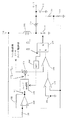
図1は本発明の第1の実施例の電流モード昇圧型スイッチングレギュレータのブロック図である。図3に示した従来の電流モード昇圧型スイッチングレギュレータに入力電圧VINおよび出力電圧VOUTから適切なスロープ補償値を出力する、スロープ補償値演算回路130を追加することで、スロープ補償回路102はスロープ補償値演算回路130の出力に応じた補償ランプ波の増加率に設定される。スロープ補償値演算回路130は抵抗120、121、123、124とアンプ122による加減算回路で構成される。
以下はスロープ補償値演算回路130が入力電圧VINおよび出力電圧VOUTに応じたスロープ補償値を出力する場合について詳細に説明する。
抵抗120、121、123、124の抵抗値をそれぞれR120、R121、R123、R124とするとアンプ122の出力電圧VCは
VC={(R123)/(R123+R124)}×{(R120+R121)/
(R120)}(VOUT)−{(R124/R120)}(VIN)
・・・(4)
となる。抵抗120、121、123、124の抵抗値について
R123+R124=R120+R121 ・・・(5)
R123=R121/2 ・・・(6)
(5)式(6)式を満たすように設定すると、(4)式は
VC={(R121)/(2×R120)}(VOUT)−2(VIN)
となり、スロープ補償値演算回路130の出力は(VOUT−2VIN)に比例する出力となる。
FIG. 1 is a block diagram of a current mode step-up switching regulator according to a first embodiment of the present invention. By adding a slope compensation
Hereinafter, a case where the slope compensation
When the resistance values of the
(R120)} (VOUT)-{(R124 / R120)} (VIN)
... (4)
It becomes. Regarding the resistance values of the
R123 = R121 / 2 (6)
(5) If it sets so that Formula (6) may be satisfy | filled, Formula (4) will be VC = {(R121) / (2 * R120)} (VOUT) -2 (VIN).
Thus, the output of the slope compensation
一方、電流モード昇圧型スイッチングレギュレータのサブハーモニック発振を防止するために必要な最小のスロープ補償値mは(3)式より、
m=(VOUT−2VIN)/(2L) ・・・(7)
となり、(VOUT−2VIN)に比例する。従ってスロープ補償値演算回路130によってスロープ補償値mが(VOUT−2VIN)に比例する構成にすることで、いかなる入力電圧VINおよび出力電圧VOUTに対してもサブハーモニック発振しない最小のスロープ補償を保った、電流モード昇圧型スイッチングレギュレータを構成できる。
On the other hand, the minimum slope compensation value m required to prevent subharmonic oscillation of the current mode boost switching regulator is
m = (VOUT−2VIN) / (2L) (7)
And is proportional to (VOUT-2VIN). Therefore, the slope compensation
図2は本発明の第2実施例の電流モード昇圧型スイッチングレギュレータのブロック図である。スロープ補償値演算回路130の分圧抵抗、抵抗123、124と帰還抵抗抵抗110、111を共用することで抵抗の素子数を削減していること以外は第1の実施例と同じである。
FIG. 2 is a block diagram of a current mode step-up switching regulator according to the second embodiment of the present invention. The present embodiment is the same as the first embodiment except that the number of resistance elements is reduced by sharing the voltage dividing resistors,
以上では電流モード昇圧型スイッチングレギュレータに適応させた場合について述べたが電流モード降圧型スイッチングレギュレータに適応する場合、コイルの電流増加率m1および電流減少率m2はそれぞれ
m1=(VIN―VOUT)/L ・・・(8)
m2=VOUT/L ・・・(9)
で与えられるので適切なスロープ補償値mは
m=(m2−m1)/2=(2VOUT−VIN)/(2L) ・・・(10)
となる。
In the above, the case where the current mode step-up switching regulator is applied has been described. However, when the current mode step-down switching regulator is applied, the current increase rate m1 and the current decrease rate m2 of the coil are m1 = (VIN−VOUT) / L, respectively. ... (8)
m2 = VOUT / L (9)
Therefore, the appropriate slope compensation value m is m = (m2−m1) / 2 = (2VOUT−VIN) / (2L) (10)
It becomes.
同様に電流モード反転型スイッチングレギュレータに適応する場合、m1、m2およびmは
m1=VIN/L ・・・(11)
m2=VOUT/L ・・・(12)
m=(m2−m1)/2=(VOUT−VIN)/(2L) ・・・(13)
で与えられる。
Similarly, when applied to a current mode inversion switching regulator, m1, m2 and m are: m1 = VIN / L (11)
m2 = VOUT / L (12)
m = (m2-m1) / 2 = (VOUT-VIN) / (2L) (13)
Given in.
従って、スロープ補償値演算回路130の分圧抵抗、抵抗123、124と帰還抵抗抵抗110、111の抵抗値を適切に設定することで電流モード降圧型スイッチングレギュレータおよび電流モード反転型スイッチングレギュレータにも同様に適応できることは明白である。
Therefore, the same applies to the current mode step-down switching regulator and the current mode inversion switching regulator by appropriately setting the resistance values of the voltage dividing resistor,
図1においてスロープ補償回路102と加算器103によって電圧信号に変換されたコイル電流信号またはスイッチ電流信号とスロープ補償回路の入力電圧VCに傾きが比例した電圧ランプ波を加算した信号をコンパレータ105の非反転電圧入力端子に入力する必要がある。
In FIG. 1, a signal obtained by adding a voltage ramp wave whose slope is proportional to the coil current signal or switch current signal converted into a voltage signal by the
図3に電圧信号に変換されたコイル電流信号またはスイッチ電流信号とスロープ補償回路の入力電圧VCに傾きが比例した電圧ランプ波を加算した信号を発生させる回路の1つの例を示す。 FIG. 3 shows an example of a circuit for generating a signal obtained by adding a coil ramp signal or a switch current signal converted into a voltage signal and a voltage ramp wave having a slope proportional to the input voltage VC of the slope compensation circuit.
pnp型バイポーラトランジスタ150、npn型バイポーラトランジスタ152、定電流源151および抵抗153で構成される電圧―電流変換回路によって入力信号VCに比例する電流を発生させ、この出力電流をPチャネル・エンハンスメント型MOSトランジスタ154、155で構成されるカレントミラーを介して容量157に注入することで容量157の両端に傾きが入力信号VCに比例する電圧ランプ波を発生させる。Nチャネル・エンハンスメント型MOSトランジスタ156は発振器の発振周期に従って前記電圧ランプ波をリセットする。また、前記電圧ランプ波はpnp型バイポーラトランジスタ158、npn型バイポーラトランジスタ160、定電流源159および抵抗161で構成される電圧―電流変換回路によって電流変換され、この電流はPチャネル・エンハンスメント型MOSトランジスタ162、163で構成されるカレントミラーを介して抵抗165に注入することで再度、電圧変換される。一方、電流センス抵抗等により電圧信号に変換されたコイル電流信号またはスイッチ電流信号は抵抗164を介して抵抗165に加算される。従って図2の回路で電圧信号に変換されたコイル電流信号またはスイッチ電流信号と傾きが入力信号VCに比例した電圧ランプ波を加算した信号が得られることは明白である。他の回路構成でも本発明の図3の回路構成と同等の結果を得ることは可能であり、本発明は図3の回路構成に言及したものではない。
A voltage-current conversion circuit comprising a pnp
100 基準電圧源
101 エラーアンプ
102 スロープ補償回路
103 加算器
104 発振器
105 コンパレータ
106 SR−ラッチ
107 スイッチ
108 コイル
109 ダイオード
110、111、120、121、123,124 抵抗
122 オペアンプ
130 スロープ補償値演算回路
150、158 pnp型バイポーラトランジスタ
152、160 npn型バイポーラトランジスタ
156 Nチャネル・エンハンスメント型MOSトランジスタ
154、155 Pチャネル・エンハンスメント型MOSトランジスタ
162,163 Pチャネル・エンハンスメント型MOSトランジスタ
151、159 定電流源
157 コンデンサ
153、161、164,165 抵抗
100
Claims (4)
Priority Applications (1)
| Application Number | Priority Date | Filing Date | Title |
|---|---|---|---|
| JP2004207224A JP2006033958A (en) | 2004-07-14 | 2004-07-14 | Switching regulator |
Applications Claiming Priority (1)
| Application Number | Priority Date | Filing Date | Title |
|---|---|---|---|
| JP2004207224A JP2006033958A (en) | 2004-07-14 | 2004-07-14 | Switching regulator |
Publications (2)
| Publication Number | Publication Date |
|---|---|
| JP2006033958A true JP2006033958A (en) | 2006-02-02 |
| JP2006033958A5 JP2006033958A5 (en) | 2007-07-26 |
Family
ID=35899625
Family Applications (1)
| Application Number | Title | Priority Date | Filing Date |
|---|---|---|---|
| JP2004207224A Withdrawn JP2006033958A (en) | 2004-07-14 | 2004-07-14 | Switching regulator |
Country Status (1)
| Country | Link |
|---|---|
| JP (1) | JP2006033958A (en) |
Cited By (23)
| Publication number | Priority date | Publication date | Assignee | Title |
|---|---|---|---|---|
| DE102006038936A1 (en) * | 2006-08-18 | 2008-02-28 | Atmel Germany Gmbh | Switching regulator, transceiver circuit and keyless access control system |
| JP2008161001A (en) * | 2006-12-26 | 2008-07-10 | Ricoh Co Ltd | Current-mode control type switching regulator and operation control method therefor |
| JP2009071978A (en) * | 2007-09-13 | 2009-04-02 | Fuji Electric Device Technology Co Ltd | Switching power supply |
| US7548049B2 (en) | 2006-12-21 | 2009-06-16 | Rohm Co., Ltd. | Switching regulator |
| JP2009153289A (en) * | 2007-12-20 | 2009-07-09 | Oki Semiconductor Co Ltd | Dc-dc converter |
| JP2009268348A (en) * | 2008-04-23 | 2009-11-12 | Honeywell Internatl Inc | Systems and methods for producing substantially constant output voltage in power source boost system |
| JP2009303303A (en) * | 2008-06-10 | 2009-12-24 | Ricoh Co Ltd | Switching regulator |
| JP2010532152A (en) * | 2007-06-26 | 2010-09-30 | ビシャイ‐シリコニックス | Current-mode boost converter with slope compensation |
| CN102025274A (en) * | 2009-09-18 | 2011-04-20 | Det国际控股有限公司 | Digital slope compensation for current mode control |
| JP2012065430A (en) * | 2010-09-15 | 2012-03-29 | Asahi Kasei Electronics Co Ltd | Control circuit for dc-dc converter and dc-dc converter |
| US8207721B2 (en) | 2007-07-27 | 2012-06-26 | Ricoh Company, Ltd. | Switching regulator capable of stable operation and improved frequency characteristics in a broad input and output voltage range and method for controlling operation thereof |
| US8471543B2 (en) | 2009-11-05 | 2013-06-25 | Renesas Electronics Corporation | DC-DC converter with slope compensation circuit and DC voltage conversion method thereof |
| US8624566B2 (en) | 2008-05-13 | 2014-01-07 | Ricoh Company, Ltd. | Current-mode control switching regulator and operations control method thereof |
| JP2014050250A (en) * | 2012-08-31 | 2014-03-17 | Nippon Soken Inc | Power conversion device |
| JP2014064417A (en) * | 2012-09-21 | 2014-04-10 | Toshiba Corp | Step-up/down type power supply circuit |
| CN104184321A (en) * | 2013-05-23 | 2014-12-03 | 美格纳半导体有限公司 | Ramp circuit and direct current dc-dc converter thereof |
| US8994353B2 (en) | 2011-09-27 | 2015-03-31 | Denso Corporation | Power converter with a pulse-width limiter that limits a drive signal pulse width according to the input voltage |
| JP2015149837A (en) * | 2014-02-06 | 2015-08-20 | セイコーインスツル株式会社 | Switching regulator control circuit and switching regulator |
| JP2016092957A (en) * | 2014-11-04 | 2016-05-23 | ローム株式会社 | Switching power unit |
| JP2017169340A (en) * | 2016-03-15 | 2017-09-21 | 富士電機株式会社 | Control circuit and slope generation circuit for switching power supply |
| CN110323956A (en) * | 2018-03-30 | 2019-10-11 | 株式会社电装 | Control equipment for electric power converter |
| CN113794372A (en) * | 2021-08-11 | 2021-12-14 | 昂宝电子(上海)有限公司 | Buck-boost converter and slope compensation circuit thereof |
| WO2023238241A1 (en) * | 2022-06-07 | 2023-12-14 | 日清紡マイクロデバイス株式会社 | Switching regulator |
-
2004
- 2004-07-14 JP JP2004207224A patent/JP2006033958A/en not_active Withdrawn
Cited By (35)
| Publication number | Priority date | Publication date | Assignee | Title |
|---|---|---|---|---|
| DE102006038936A1 (en) * | 2006-08-18 | 2008-02-28 | Atmel Germany Gmbh | Switching regulator, transceiver circuit and keyless access control system |
| US7728717B2 (en) | 2006-08-18 | 2010-06-01 | Atmel Automotive Gmbh | Switching regulator, transceiver circuit, and keyless access control system |
| US7548049B2 (en) | 2006-12-21 | 2009-06-16 | Rohm Co., Ltd. | Switching regulator |
| KR100953362B1 (en) | 2006-12-26 | 2010-04-20 | 가부시키가이샤 리코 | Current-mode controlled switching regulator and control method therefor |
| JP2008161001A (en) * | 2006-12-26 | 2008-07-10 | Ricoh Co Ltd | Current-mode control type switching regulator and operation control method therefor |
| US7876073B2 (en) | 2006-12-26 | 2011-01-25 | Ricoh Company, Ltd. | Switching regulator with slope compensation and control method therefor |
| US9423812B2 (en) | 2007-06-26 | 2016-08-23 | Vishay-Siliconix | Current mode boost converter using slope compensation |
| JP2010532152A (en) * | 2007-06-26 | 2010-09-30 | ビシャイ‐シリコニックス | Current-mode boost converter with slope compensation |
| JP2012239381A (en) * | 2007-06-26 | 2012-12-06 | Vishay-Siliconix | Current mode boost converter using slope compensation |
| US8207721B2 (en) | 2007-07-27 | 2012-06-26 | Ricoh Company, Ltd. | Switching regulator capable of stable operation and improved frequency characteristics in a broad input and output voltage range and method for controlling operation thereof |
| JP2009071978A (en) * | 2007-09-13 | 2009-04-02 | Fuji Electric Device Technology Co Ltd | Switching power supply |
| JP2009153289A (en) * | 2007-12-20 | 2009-07-09 | Oki Semiconductor Co Ltd | Dc-dc converter |
| JP2009268348A (en) * | 2008-04-23 | 2009-11-12 | Honeywell Internatl Inc | Systems and methods for producing substantially constant output voltage in power source boost system |
| US8624566B2 (en) | 2008-05-13 | 2014-01-07 | Ricoh Company, Ltd. | Current-mode control switching regulator and operations control method thereof |
| JP2009303303A (en) * | 2008-06-10 | 2009-12-24 | Ricoh Co Ltd | Switching regulator |
| CN102025274A (en) * | 2009-09-18 | 2011-04-20 | Det国际控股有限公司 | Digital slope compensation for current mode control |
| US8471543B2 (en) | 2009-11-05 | 2013-06-25 | Renesas Electronics Corporation | DC-DC converter with slope compensation circuit and DC voltage conversion method thereof |
| JP2012065430A (en) * | 2010-09-15 | 2012-03-29 | Asahi Kasei Electronics Co Ltd | Control circuit for dc-dc converter and dc-dc converter |
| US8994353B2 (en) | 2011-09-27 | 2015-03-31 | Denso Corporation | Power converter with a pulse-width limiter that limits a drive signal pulse width according to the input voltage |
| JP2014050250A (en) * | 2012-08-31 | 2014-03-17 | Nippon Soken Inc | Power conversion device |
| US9184736B2 (en) | 2012-08-31 | 2015-11-10 | Denso Corporation | Current mode controlled power converter |
| JP2014064417A (en) * | 2012-09-21 | 2014-04-10 | Toshiba Corp | Step-up/down type power supply circuit |
| CN104184321A (en) * | 2013-05-23 | 2014-12-03 | 美格纳半导体有限公司 | Ramp circuit and direct current dc-dc converter thereof |
| KR101796811B1 (en) | 2013-05-23 | 2017-11-13 | 매그나칩 반도체 유한회사 | Ramp citcuit and dc-dc converter thereof |
| CN104184321B (en) * | 2013-05-23 | 2018-06-01 | 美格纳半导体有限公司 | Ramp circuit and its DC-DC converter |
| JP2015149837A (en) * | 2014-02-06 | 2015-08-20 | セイコーインスツル株式会社 | Switching regulator control circuit and switching regulator |
| JP2016092957A (en) * | 2014-11-04 | 2016-05-23 | ローム株式会社 | Switching power unit |
| JP2017169340A (en) * | 2016-03-15 | 2017-09-21 | 富士電機株式会社 | Control circuit and slope generation circuit for switching power supply |
| CN110323956A (en) * | 2018-03-30 | 2019-10-11 | 株式会社电装 | Control equipment for electric power converter |
| JP2019180178A (en) * | 2018-03-30 | 2019-10-17 | 株式会社Soken | Controller of power converter |
| JP7054358B2 (en) | 2018-03-30 | 2022-04-13 | 株式会社Soken | Power converter control device |
| CN110323956B (en) * | 2018-03-30 | 2023-12-22 | 株式会社电装 | Control apparatus for power converter |
| CN113794372A (en) * | 2021-08-11 | 2021-12-14 | 昂宝电子(上海)有限公司 | Buck-boost converter and slope compensation circuit thereof |
| CN113794372B (en) * | 2021-08-11 | 2023-09-29 | 昂宝电子(上海)有限公司 | Buck-boost converter and slope compensation circuit thereof |
| WO2023238241A1 (en) * | 2022-06-07 | 2023-12-14 | 日清紡マイクロデバイス株式会社 | Switching regulator |
Similar Documents
| Publication | Publication Date | Title |
|---|---|---|
| JP2006033958A (en) | Switching regulator | |
| KR100953362B1 (en) | Current-mode controlled switching regulator and control method therefor | |
| US8624566B2 (en) | Current-mode control switching regulator and operations control method thereof | |
| JP5211959B2 (en) | DC-DC converter | |
| JP5091027B2 (en) | Switching regulator | |
| JP5151830B2 (en) | Current mode control type DC-DC converter | |
| US7180274B2 (en) | Switching voltage regulator operating without a discontinuous mode | |
| JP5104145B2 (en) | Switching power supply | |
| US7327124B2 (en) | Control apparatus and method for a boost-inverting converter | |
| US20070085523A1 (en) | Dc-dc converter | |
| JP2009303317A (en) | Reference voltage generating circuit and dc-dc converter with that reference voltage generating circuit | |
| JP2008131746A (en) | Step-up/down switching regulator | |
| JP2009219179A (en) | Current mode control type switching regulator | |
| JP2013165537A (en) | Switching regulator, control method thereof, and power supply device | |
| KR20080025314A (en) | Method and circuit for controlling dc-dc converter | |
| JP2009153289A (en) | Dc-dc converter | |
| JP6015370B2 (en) | Switching power supply | |
| JP5470772B2 (en) | Current mode control switching regulator | |
| US11750078B2 (en) | Adaptive off-time or on-time DC-DC converter | |
| JP4791839B2 (en) | Current mode control type DC-DC converter | |
| JP2020065402A (en) | Switching regulator | |
| JP4487649B2 (en) | Control device for step-up / step-down DC-DC converter | |
| JP4548100B2 (en) | DC-DC converter | |
| CN109256948B (en) | Switching regulator | |
| JP4438507B2 (en) | Current mode step-down switching regulator |
Legal Events
| Date | Code | Title | Description |
|---|---|---|---|
| A521 | Written amendment |
Effective date: 20070607 Free format text: JAPANESE INTERMEDIATE CODE: A523 |
|
| A621 | Written request for application examination |
Free format text: JAPANESE INTERMEDIATE CODE: A621 Effective date: 20070607 |
|
| RD01 | Notification of change of attorney |
Free format text: JAPANESE INTERMEDIATE CODE: A7421 Effective date: 20091105 |
|
| RD01 | Notification of change of attorney |
Free format text: JAPANESE INTERMEDIATE CODE: A7421 Effective date: 20091112 |
|
| A977 | Report on retrieval |
Effective date: 20100114 Free format text: JAPANESE INTERMEDIATE CODE: A971007 |
|
| A131 | Notification of reasons for refusal |
Effective date: 20100119 Free format text: JAPANESE INTERMEDIATE CODE: A131 |
|
| A761 | Written withdrawal of application |
Free format text: JAPANESE INTERMEDIATE CODE: A761 Effective date: 20100312 |