JP5477359B2 - Display device - Google Patents
Display device Download PDFInfo
- Publication number
- JP5477359B2 JP5477359B2 JP2011241880A JP2011241880A JP5477359B2 JP 5477359 B2 JP5477359 B2 JP 5477359B2 JP 2011241880 A JP2011241880 A JP 2011241880A JP 2011241880 A JP2011241880 A JP 2011241880A JP 5477359 B2 JP5477359 B2 JP 5477359B2
- Authority
- JP
- Japan
- Prior art keywords
- pixel
- light emitting
- emitting element
- capacitor
- drive transistor
- Prior art date
- Legal status (The legal status is an assumption and is not a legal conclusion. Google has not performed a legal analysis and makes no representation as to the accuracy of the status listed.)
- Expired - Fee Related
Links
Images


Classifications
-
- Y02B20/42—
Landscapes
- Electroluminescent Light Sources (AREA)
- Control Of Indicators Other Than Cathode Ray Tubes (AREA)
- Control Of El Displays (AREA)
Description
本発明は、画素毎に配した発光素子を電流駆動する画素回路に関する。又この画素回路がマトリクス状(行列状)に配列された表示装置であって、特に各画素回路内に設けた絶縁ゲート型電界効果トランジスタによって、有機ELなどの発光素子に通電する電流量を制御する、いわゆるアクティブマトリクス型の表示装置に関する。 The present invention relates to a pixel circuit that current-drives a light emitting element arranged for each pixel. In addition, this pixel circuit is a display device arranged in a matrix (matrix), and the amount of current supplied to a light emitting element such as an organic EL is controlled by an insulated gate field effect transistor provided in each pixel circuit. The present invention relates to a so-called active matrix display device.
画像表示装置、例えば液晶ディスプレイなどでは、多数の液晶画素をマトリクス状に並べ、表示すべき画像情報に応じて画素毎に入射光の透過強度又は反射強度を制御することによって画像を表示する。これは、有機EL素子を画素に用いた有機ELディスプレイなどにおいても同様であるが、液晶画素と異なり有機EL素子は自発光素子である。その為、有機ELディスプレイは液晶ディスプレイに比べて画像の視認性が高く、バックライトが不要であり、応答速度が高いなどの利点を有する。又、各発光素子の輝度レベル(階調)はそれに流れる電流値によって制御可能であり、いわゆる電流制御型であるという点で液晶ディスプレイなどの電圧制御型とは大きく異なる。 In an image display device such as a liquid crystal display, an image is displayed by arranging a large number of liquid crystal pixels in a matrix and controlling the transmission intensity or reflection intensity of incident light for each pixel in accordance with image information to be displayed. This also applies to an organic EL display using an organic EL element as a pixel, but unlike a liquid crystal pixel, the organic EL element is a self-luminous element. Therefore, the organic EL display has advantages such as higher image visibility than the liquid crystal display, no backlight, and high response speed. Further, the luminance level (gradation) of each light emitting element can be controlled by the value of the current flowing therethrough, and is greatly different from a voltage control type such as a liquid crystal display in that it is a so-called current control type.
有機ELディスプレイにおいては、液晶ディスプレイと同様、その駆動方式として単純マトリクス方式とアクティブマトリクス方式とがある。前者は構造が単純であるものの、大型且つ高精細のディスプレイの実現が難しいなどの問題がある為、現在はアクティブマトリクス方式の開発が盛んに行なわれている。この方式は、各画素回路内部の発光素子に流れる電流を、画素回路内部に設けた能動素子(一般には薄膜トランジスタ、TFT)によって制御するものであり、以下の特許文献に記載がある。 In the organic EL display, similarly to the liquid crystal display, there are a simple matrix method and an active matrix method as driving methods. Although the former has a simple structure, there is a problem that it is difficult to realize a large-sized and high-definition display. Therefore, the active matrix method is actively developed at present. In this method, a current flowing through a light emitting element in each pixel circuit is controlled by an active element (generally a thin film transistor or TFT) provided in the pixel circuit, and is described in the following patent documents.
従来の画素回路は、制御信号を供給する行状の走査線と映像信号を供給する列状の信号線とが交差する部分に配され、少なくともサンプリングトランジスタと画素容量とドライブトランジスタと発光素子とを含む。サンプリングトランジスタは、走査線から供給される制御信号に応じ導通して信号線から供給された映像信号をサンプリングする。画素容量は、サンプリングされた映像信号に応じた入力電圧を保持する。ドライブトランジスタは、画素容量に保持された入力電圧に応じて所定の発光期間に出力電流を供給する。尚一般に、出力電流はドライブトランジスタのチャネル領域のキャリア移動度及び閾電圧に対して依存性を有する。発光素子は、ドライブトランジスタから供給された出力電流により映像信号に応じた輝度で発光する。 A conventional pixel circuit is arranged at a portion where a row scanning line for supplying a control signal and a column signal line for supplying a video signal intersect, and includes at least a sampling transistor, a pixel capacitor, a drive transistor, and a light emitting element. . The sampling transistor conducts in response to the control signal supplied from the scanning line and samples the video signal supplied from the signal line. The pixel capacitance holds an input voltage corresponding to the sampled video signal. The drive transistor supplies an output current during a predetermined light emission period in accordance with the input voltage held in the pixel capacitor. In general, the output current depends on the carrier mobility and threshold voltage of the channel region of the drive transistor. The light emitting element emits light with luminance according to the video signal by the output current supplied from the drive transistor.
ドライブトランジスタは、画素容量に保持された入力電圧をゲートに受けてソース/ドレイン間に出力電流を流し、発光素子に通電する。一般に発光素子の発光輝度は通電量に比例している。更にドライブトランジスタの出力電流供給量はゲート電圧すなわち画素容量に書き込まれた入力電圧によって制御される。従来の画素回路は、ドライブトランジスタのゲートに印加される入力電圧を入力映像信号に応じて変化させることで、発光素子に供給する電流量を制御している。 The drive transistor receives an input voltage held in the pixel capacitor at the gate, causes an output current to flow between the source and the drain, and energizes the light emitting element. In general, the light emission luminance of a light emitting element is proportional to the amount of current applied. Further, the output current supply amount of the drive transistor is controlled by the gate voltage, that is, the input voltage written in the pixel capacitor. The conventional pixel circuit controls the amount of current supplied to the light emitting element by changing the input voltage applied to the gate of the drive transistor in accordance with the input video signal.
ここでドライブトランジスタの動作特性は以下の式1で表わされる。
Ids=(1/2)μ(W/L)Cox(Vgs−Vth)2・・・式1
このトランジスタ特性式1において、Idsはソース/ドレイン間に流れるドレイン電流を表わしており、画素回路では発光素子に供給される出力電流である。Vgsはソースを基準としてゲートに印加されるゲート電圧を表わしており、画素回路では上述した入力電圧である。Vthはトランジスタの閾電圧である。又μはトランジスタのチャネルを構成する半導体薄膜の移動度を表わしている。その他Wはチャネル幅を表わし、Lはチャネル長を表わし、Coxはゲート容量を表わしている。このトランジスタ特性式1から明らかな様に、薄膜トランジスタは飽和領域で動作する時、ゲート電圧Vgsが閾電圧Vthを超えて大きくなると、オン状態となってドレイン電流Idsが流れる。原理的に見ると上記のトランジスタ特性式1が示す様に、ゲート電圧Vgsが一定であれば常に同じ量のドレイン電流Idsが発光素子に供給される。従って、画面を構成する各画素に全て同一のレベルの映像信号を供給すれば、全画素が同一輝度で発光し、画面の一様性(ユニフォーミティ)が得られるはずである。
Here, the operating characteristic of the drive transistor is expressed by the following
Ids = (1/2) μ (W / L) Cox (Vgs−Vth) 2
In the
しかしながら実際には、ポリシリコンなどの半導体薄膜で構成された薄膜トランジスタ(TFT)は、個々のデバイス特性にばらつきがある。特に、閾電圧Vthは一定ではなく、各画素毎にばらつきがある。前述のトランジスタ特性式1から明らかな様に、各ドライブトランジスタの閾電圧Vthがばらつくと、ゲート電圧Vgsが一定であっても、ドレイン電流Idsにばらつきが生じ、画素毎に輝度がばらついてしまう為、画面のユニフォーミティを損なう。従来からドライブトランジスタの閾電圧のばらつきをキャンセルする機能を組み込んだ画素回路が開発されており、例えば前記の特許文献3に開示がある。
However, in reality, thin film transistors (TFTs) composed of semiconductor thin films such as polysilicon have variations in individual device characteristics. In particular, the threshold voltage Vth is not constant and varies from pixel to pixel. As apparent from the
閾電圧のばらつきをキャンセルする機能を組み込んだ画素回路は、ある程度画面のユニフォーミティを改善することが可能である。しかしながら、ポリシリコン薄膜トランジスタの特性は、閾電圧ばかりでなく移動度μも素子毎にばらつきがある。前述のトランジスタ特性式1から明らかな様に、移動度μがばらつくと、ゲート電圧Vgsが一定であってもドレイン電流Idsにばらつきが出てしまう。この結果発光輝度が画素毎に変化する為画面のユニフォーミティを損なうという課題がある。
A pixel circuit incorporating a function for canceling variations in threshold voltage can improve screen uniformity to some extent. However, the characteristics of polysilicon thin film transistors vary not only in the threshold voltage but also in the mobility μ from element to element. As apparent from the
上述した従来の技術の課題に鑑み、本発明は移動度の影響をキャンセルし、以ってドライブトランジスタが供給するドレイン電流(出力電流)のばらつきを補償可能な画素回路及び表示装置を提供することを目的とする。特に、移動度の影響をキャンセルするために必要な補正動作のマージンを確保し、以って画素回路及び表示装置の動作を安定化することを目的とする。かかる目的を達成するために以下の手段を講じた。即ち本発明は、制御信号を供給する行状の走査線と映像信号を供給する列状の信号線とが交差する部分に配され、少なくともサンプリングトランジスタと、これに接続する画素容量と、これに接続するドライブトランジスタと、これに接続する発光素子とを含み、前記サンプリングトランジスタは、走査線から供給される制御信号に応じ導通して信号線から供給された映像信号を該画素容量にサンプリングし、前記画素容量は、該サンプリングされた映像信号に応じて該ドライブトランジスタのゲートに入力電圧を印加し、前記ドライブトランジスタは、該入力電圧に応じた出力電流を該発光素子に供給し、該出力電流は該ドライブトランジスタのチャネル領域のキャリア移動度に対して依存性を有し、前記発光素子は、該ドライブトランジスタから供給された出力電流により該映像信号に応じた輝度で発光する画素回路において、該出力電流のキャリア移動度に対する依存性を打ち消すために、該画素容量にサンプリングされる該入力電圧を補正する補正手段を備えており、前記補正手段は走査線から供給される制御信号に応じて動作し、該ドライブトランジスタから出力電流を取り出し、これを該発光素子の有する容量及び該画素容量に流し込む様にして該入力電圧を補正し、該発光素子の容量に足される追加容量を備えており、該ドライブトランジスタから取り出された出力電流の一部を該追加容量にも流し、以って該補正手段の動作に時間的な余裕を与えることを特徴とする。 In view of the above-described problems of the conventional technology, the present invention provides a pixel circuit and a display device capable of canceling the influence of mobility and compensating for variations in drain current (output current) supplied by a drive transistor. With the goal. In particular, an object is to secure a margin for a correction operation necessary to cancel the influence of mobility, and thereby stabilize the operation of the pixel circuit and the display device. In order to achieve this purpose, the following measures were taken. That is, according to the present invention, at least a sampling transistor, a pixel capacitor connected to the sampling transistor, and a pixel capacitor connected to the row scanning line that supplies a control signal and a column signal line that supplies a video signal are connected. A sampling transistor that conducts in response to a control signal supplied from a scanning line and samples a video signal supplied from the signal line into the pixel capacitor, The pixel capacitor applies an input voltage to the gate of the drive transistor according to the sampled video signal, the drive transistor supplies an output current according to the input voltage to the light emitting element, and the output current is The drive transistor has a dependence on the carrier mobility of the channel region, and the light emitting element has the drive transistor. In the pixel circuit that emits light with the luminance corresponding to the video signal by the output current supplied from the image sensor, the input voltage sampled in the pixel capacitor is corrected in order to cancel the dependence of the output current on the carrier mobility. And a correction unit that operates according to a control signal supplied from a scanning line, extracts an output current from the drive transistor, and flows the output current into the capacitor and the pixel capacitor of the light-emitting element. The input voltage is corrected, and an additional capacitor added to the capacitance of the light emitting element is provided, and a part of the output current extracted from the drive transistor is also passed to the additional capacitor, whereby the correcting means It is characterized in that a time margin is given to the operation.
好ましくは、前記サンプリングトランジスタ、ドライブトランジスタ及び補正手段は、絶縁基板上に形成された薄膜トランジスタからなり、前記画素容量と追加容量は、該絶縁基板上に形成された薄膜容量素子からなる。又前記ドライブトランジスタは、その出力電流がチャネル領域のキャリア移動度に加え閾電圧に対しても依存性を有し、前記補正手段は、該出力電流の閾電圧に対する依存性を打ち消すために、あらかじめ該ドライブトランジスタの閾電圧を検出し、且つ該検出された閾電圧を該入力電圧に足し込む様にしている。又前記発光素子はアノード及びカソードを備えたダイオード型の発光素子からなり、アノード側が該ドライブトランジスタのソースに接続する一方カソード側が接地されており、前記追加容量は、一方の端子が該発光素子のアノードに接続し、他方の端子が、所定の固定電位に接続されている。前記追加容量の他方の端子が接続する所定の固定電位は、該発光素子のカソード側になる接地電位、画素回路の正側電源電位又は負側電源電位から選択できる。又各画素回路は、赤色発光素子、緑色発光素子又は青色発光素子のいずれかを備えており、各画素回路に形成された前記追加容量は、各色発光素子ごとに異なる容量値を有し、以って各画素回路に形成された各補正手段の動作に要する時間を均一化する。又各画素回路に形成された追加容量の容量値に不足がある場合、隣接する画素回路に形成された追加容量を利用して該不足を補うようにしている。一態様では前記補正手段は、該映像信号が該画素容量にサンプリングされている状態で該ドライブトランジスタから出力電流を取り出し、これを該画素容量に負帰還して該入力電圧を補正する。 Preferably, the sampling transistor, the drive transistor, and the correcting unit are formed of a thin film transistor formed on an insulating substrate, and the pixel capacitor and the additional capacitor are formed of a thin film capacitor element formed on the insulating substrate. The drive transistor has an output current dependent on the threshold voltage in addition to the carrier mobility of the channel region, and the correction means cancels the dependency of the output current on the threshold voltage in advance. A threshold voltage of the drive transistor is detected, and the detected threshold voltage is added to the input voltage. The light emitting element is a diode type light emitting element having an anode and a cathode, the anode side is connected to the source of the drive transistor, the cathode side is grounded, and the additional capacitor has one terminal connected to the light emitting element. Connected to the anode, the other terminal is connected to a predetermined fixed potential. The predetermined fixed potential connected to the other terminal of the additional capacitor can be selected from the ground potential on the cathode side of the light emitting element, the positive power supply potential or the negative power supply potential of the pixel circuit. Each pixel circuit includes any one of a red light emitting element, a green light emitting element, and a blue light emitting element, and the additional capacitance formed in each pixel circuit has a different capacitance value for each color light emitting element. Thus, the time required for the operation of each correction means formed in each pixel circuit is made uniform. In addition, when there is a shortage in the capacitance value of the additional capacitor formed in each pixel circuit, the shortage is compensated by using the additional capacitor formed in the adjacent pixel circuit. In one aspect, the correcting means extracts an output current from the drive transistor in a state where the video signal is sampled in the pixel capacitor, and negatively feeds back the output current to the pixel capacitor to correct the input voltage.
また本発明は、画素アレイ部とスキャナ部と信号部とを含み、前記画素アレイ部は、行状に配された走査線と列状に配された信号線と両者が交差する部分に配された行列状の画素とからなり、前記信号部は、該信号線に映像信号を供給し、前記スキャナ部は、該走査線に制御信号を供給して順次行ごとに画素を走査し、各画素は、少なくともサンプリングトランジスタと、これに接続する画素容量と、これに接続するドライブトランジスタと、これに接続する発光素子とを含み、前記サンプリングトランジスタは、走査線から供給される制御信号に応じ導通して信号線から供給された映像信号を該画素容量にサンプリングし、前記画素容量は、該サンプリングされた映像信号に応じて該ドライブトランジスタのゲートに入力電圧を印加し、前記ドライブトランジスタは、該入力電圧に応じた出力電流を該発光素子に供給し、該出力電流は該ドライブトランジスタのチャネル領域のキャリア移動度に対して依存性を有し、前記発光素子は、該ドライブトランジスタから供給された出力電流により該映像信号に応じた輝度で発光する表示装置において、各画素は、該出力電流のキャリア移動度に対する依存性を打ち消すために、該画素容量にサンプリングされる該入力電圧を補正する補正手段を備えており、前記補正手段は走査線から供給される制御信号に応じて動作し、該ドライブトランジスタから出力電流を取り出し、これを該発光素子の有する容量及び該画素容量に流し込む様にして該入力電圧を補正し、該発光素子の容量に足される追加容量を備えており、該ドライブトランジスタから取り出された出力電流の一部を該追加容量にも流し、以って該補正手段の動作に時間的な余裕を与えることを特徴とする。 The present invention also includes a pixel array section, a scanner section, and a signal section, and the pixel array section is disposed at a portion where the scanning lines arranged in rows and the signal lines arranged in columns intersect with each other. The signal unit supplies a video signal to the signal line, the scanner unit supplies a control signal to the scanning line, and sequentially scans the pixels for each row. Including at least a sampling transistor, a pixel capacitor connected thereto, a drive transistor connected thereto, and a light emitting element connected thereto, wherein the sampling transistor is turned on in response to a control signal supplied from a scanning line. A video signal supplied from a signal line is sampled in the pixel capacitor, and the pixel capacitor applies an input voltage to the gate of the drive transistor in accordance with the sampled video signal, The drive transistor supplies an output current corresponding to the input voltage to the light emitting element, and the output current has a dependency on the carrier mobility of the channel region of the drive transistor, and the light emitting element In a display device that emits light with a luminance corresponding to the video signal by an output current supplied from a transistor, each pixel is sampled in the pixel capacitance in order to cancel the dependence of the output current on carrier mobility. Compensating means for correcting the voltage is provided, and the correcting means operates in response to a control signal supplied from the scanning line, extracts an output current from the drive transistor, and uses the output current as the capacitance of the light emitting element and the pixel capacitance The input voltage is corrected so as to flow into the light source, and an additional capacity added to the capacity of the light emitting element is provided. A portion of the output current drawn from the data flow to the additional capacity, characterized in providing a time margin to operation of said correcting means I following.
好ましくは、前記サンプリングトランジスタ、ドライブトランジスタ及び補正手段は、絶縁基板上に形成された薄膜トランジスタからなり、前記画素容量と追加容量は、該絶縁基板上に形成された薄膜容量素子からなる。又前記ドライブトランジスタは、その出力電流がチャネル領域のキャリア移動度に加え閾電圧に対しても依存性を有し、前記補正手段は、該出力電流の閾電圧に対する依存性を打ち消すために、あらかじめ該ドライブトランジスタの閾電圧を検出し、且つ該検出された閾電圧を該入力電圧に足し込む様にしている。また前記発光素子はアノード及びカソードを備えたダイオード型の発光素子からなり、アノード側が該ドライブトランジスタのソースに接続する一方カソード側が接地されており、前記追加容量は、一方の端子が該発光素子のアノードに接続し、他方の端子が、所定の固定電位に接続されている。前記追加容量の他方の端子が接続する所定の固定電位は、該発光素子のカソード側になる接地電位、該画素アレイ部の正側電源電位又は負側電源電位から選択できる。又各画素は、赤色発光素子、緑色発光素子又は青色発光素子のいずれかを備えており、各画素に形成された前記追加容量は、各色発光素子ごとに異なる容量値を有し、以って各画素に形成された各補正手段の動作に要する時間を均一化する。又各画素に形成された追加容量の容量値に不足がある場合、隣接する画素に形成された追加容量を利用して該不足を補うようにしている。一態様では前記補正手段は、該映像信号が該画素容量にサンプリングされている状態で該ドライブトランジスタから出力電流を取り出し、これを該画素容量に負帰還して該入力電圧を補正する。 Preferably, the sampling transistor, the drive transistor, and the correcting unit are formed of a thin film transistor formed on an insulating substrate, and the pixel capacitor and the additional capacitor are formed of a thin film capacitor element formed on the insulating substrate. The drive transistor has an output current dependent on the threshold voltage in addition to the carrier mobility of the channel region, and the correction means cancels the dependency of the output current on the threshold voltage in advance. A threshold voltage of the drive transistor is detected, and the detected threshold voltage is added to the input voltage. The light emitting element is a diode type light emitting element having an anode and a cathode, the anode side is connected to the source of the drive transistor, the cathode side is grounded, and the additional capacitor has one terminal connected to the light emitting element. Connected to the anode, the other terminal is connected to a predetermined fixed potential. The predetermined fixed potential connected to the other terminal of the additional capacitor can be selected from the ground potential on the cathode side of the light emitting element, the positive power supply potential or the negative power supply potential of the pixel array section. Each pixel includes any one of a red light emitting element, a green light emitting element, and a blue light emitting element, and the additional capacitance formed in each pixel has a capacitance value that is different for each color light emitting element. The time required for the operation of each correction means formed in each pixel is made uniform. In addition, when there is a deficiency in the capacitance value of the additional capacitance formed in each pixel, the deficiency is compensated by using the additional capacitance formed in the adjacent pixel. In one aspect, the correcting means extracts an output current from the drive transistor in a state where the video signal is sampled in the pixel capacitor, and negatively feeds back the output current to the pixel capacitor to correct the input voltage.
本発明によれば、画素回路並びにこれを集積形成した表示装置は、例えば電圧駆動方式で閾電圧及び移動度のばらつきを補正可能な補正手段を備えている。補正手段を含んだ画素回路は複数の薄膜トランジスタ(TFT)などで構成されており、ガラスなどの絶縁基板上に集積形成されている。本発明ではこの絶縁基板に薄膜容量素子で追加の容量を形成している。この追加容量は発光素子の容量成分と並列に接続している。かかる構成により、移動度補正に利用するトータルの容量を大きくとることが出来る。この結果移動度のばらつき補正に要する動作時間を長く設定することが可能である。即ち移動度補正期間の設定マージンを上げることが可能となり、これにより各画素回路の補正動作の安定化を達成できる。
カラー表示装置の場合、各画素回路は赤色発光素子、緑色発光素子または青色発光素子のいずれかを備えている。一般に、発光素子は色毎に発光面積や発光材料が異なっており、これに応じて容量成分が色毎に異なっている。この場合、追加容量を各発光素子毎に変えることで、移動度補正期間を各色画素で同一に設定することが可能である。全ての画素で移動度補正動作に要する時間を共通に出来るので、画素アレイの動作制御が容易になる。
赤色(R)画素、緑色(G)画素及び青色(B)画素間でホワイトバランスをとる場合や、RGB画素間で発光素子の特性が大きく異なる場合、RGB画素間で必要とされる追加容量の大きさに顕著な差が生じる場合がある。このときには、RBG画素間で追加容量の割付に工夫をすることも可能である。具体的には、ある色の画素回路に形成された追加容量の容量値に不足がある場合、隣接する別の色の画素回路に形成された追加容量を利用してその不足を補うことが出来る。これにより、RGB画素回路を含んだ表示装置の移動度補正期間を各色画素で共通に設定することが出来る。
According to the present invention, the pixel circuit and the display device integrated with the pixel circuit are provided with correction means capable of correcting variations in threshold voltage and mobility by, for example, a voltage driving method. The pixel circuit including the correcting means is composed of a plurality of thin film transistors (TFTs) and is integrated on an insulating substrate such as glass. In the present invention, an additional capacitor is formed on the insulating substrate with a thin film capacitor. This additional capacitance is connected in parallel with the capacitance component of the light emitting element. With this configuration, the total capacity used for mobility correction can be increased. As a result, it is possible to set a longer operation time for correcting the variation in mobility. In other words, it becomes possible to increase the setting margin for the mobility correction period, thereby stabilizing the correction operation of each pixel circuit.
In the case of a color display device, each pixel circuit includes any one of a red light emitting element, a green light emitting element, and a blue light emitting element. In general, a light emitting element has a different light emitting area and light emitting material for each color, and accordingly, a capacitance component differs for each color. In this case, the mobility correction period can be set to be the same for each color pixel by changing the additional capacitance for each light emitting element. Since the time required for the mobility correction operation can be made common to all the pixels, the operation control of the pixel array becomes easy.
When white balance is achieved among red (R) pixels, green (G) pixels, and blue (B) pixels, or when the characteristics of light emitting elements differ greatly between RGB pixels, the additional capacitance required between RGB pixels There may be significant differences in size. At this time, it is possible to devise the allocation of the additional capacity between the RBG pixels. Specifically, when there is a shortage in the capacitance value of the additional capacitor formed in the pixel circuit of a certain color, the shortage can be compensated by using the additional capacitor formed in the pixel circuit of another adjacent color. . Thereby, the mobility correction period of the display device including the RGB pixel circuit can be set in common for each color pixel.
以下図面を参照して本発明の実施の形態を詳細に説明する。図1は、本発明にかかる表示装置の基本構成を示す模式的なブロック図である。図示する様に、アクティブマトリクス表示装置は主要部となる画素アレイ1と周辺の回路部とで構成されている。周辺の回路部は水平セレクタ3、ライトスキャナ4、ドライブスキャナ5、補正用スキャナ7などを含んでいる。画素アレイ1は行状の走査線WSと列状の信号線SLと両者の交差する部分にマトリクス状に配列した画素R,G,Bとで構成されている。カラー表示を可能とする為、RGBの三原色画素を用意しているが、本発明はこれに限られるものではない。各画素R,G,Bは夫々画素回路2で構成されている。信号線SLは水平セレクタ3によって駆動される。水平セレクタ3は信号部を構成し、信号線SLに映像信号を供給する。走査線WSはライトスキャナ4によって走査される。尚、走査線WSと平行に別の走査線DS及びAZも配線されている。走査線DSはドライブスキャナ5によって走査される。走査線AZは補正用スキャナ7によって走査される。ライトスキャナ4、ドライブスキャナ5及び補正用スキャナ7はスキャナ部を構成しており、1水平期間毎画素の行を順次走査する。各画素回路2は走査線WSによって選択された時信号線SLから映像信号をサンプリングする。更に走査線DSによって選択された時、サンプリングされた映像信号に応じて画素回路2内に含まれている発光素子を駆動する。加えて画素回路2は走査線AZによって走査された時、あらかじめ決められた補正動作を行なう。
Hereinafter, embodiments of the present invention will be described in detail with reference to the drawings. FIG. 1 is a schematic block diagram showing a basic configuration of a display device according to the present invention. As shown in the figure, the active matrix display device includes a
上述した画素アレイ1は通常ガラスなどの絶縁基板上に形成されており、フラットパネルとなっている。各画素回路2はアモルファスシリコン薄膜トランジスタ(TFT)又は低温ポリシリコンTFTで形成されている。アモルファスシリコンTFTの場合、スキャナ部はパネルとは別のTABなどで構成され、フレキシブルケーブルにてフラットパネルに接続される。低温ポリシリコンTFTの場合、信号部及びスキャナ部も同じ低温ポリシリコンTFTで形成できるので、フラットパネル上に画素アレイ部と信号部とスキャナ部を一体的に形成できる。
The
図2は、本発明にかかる表示装置の第1実施形態を示す回路図である。図示する様に、アクティブマトリクス表示装置は主要部となる画素アレイ1と周辺の回路部とで構成されている。周辺の回路部は水平セレクタ3、ライトスキャナ4、ドライブスキャナ5、第一補正用スキャナ71、第二補正用スキャナ72などを含んでいる。画素アレイ1は行状の走査線WSと列状の信号線SLと両者の交差する部分にマトリクス状に配列した画素回路2とで構成されている。図では理解を容易にする為、1個の画素回路2のみを拡大表示してある。信号線SLは水平セレクタ3によって駆動される。水平セレクタ3は信号部を構成し、信号線SLに映像信号を供給する。走査線WSはライトスキャナ4によって走査される。なお、走査線WSと平行に別の走査線DS,AZ1及びAZ2も配線されている。走査線DSはドライブスキャナ5によって走査される。走査線AZ1は第一補正用スキャナ71によって走査される。走査線AZ2は第二補正用スキャナ72によって走査される。ライトスキャナ4、ドライブスキャナ5、第一補正用スキャナ71及び第二補正用スキャナ72はスキャナ部を構成しており、1水平期間ごと画素の行を順次走査する。各画素回路2は走査線WSによって選択されたとき信号線SLから映像信号をサンプリングする。さらに走査線DSによって選択されたとき、サンプリングされた映像信号に応じて画素回路2内に含まれている発光素子ELを駆動する。加えて画素回路2は走査線AZ1,AZ2によって走査された時、予め決められた補正動作を行う。
FIG. 2 is a circuit diagram showing a first embodiment of a display device according to the present invention. As shown in the figure, the active matrix display device includes a
画素回路2は、5個の薄膜トランジスタTr1〜Tr4及びTrdと2個の容量素子Cs,Csubと1個の発光素子ELとで構成されている。一方の容量素子Csは画素容量である。他方の容量素子Csubは本発明に従って特に設けられた追加容量である。なお、図2では理解を容易にするため発光素子ELの容量成分を容量素子Coledとして表してある。トランジスタTr1〜Tr3とTrdはNチャネル型のポリシリコンTFTである。トランジスタTr4のみPチャネル型のポリシリコンTFTである。前述したように容量素子Csは本画素回路2の画素容量を構成している。発光素子ELは例えばアノード及びカソードを備えたダイオード型の有機EL素子である。但し本発明はこれに限られるものではなく、発光素子は一般的に電流駆動で発光する全てのデバイスを含む。
The
画素回路2の中心となるドライブトランジスタTrdはそのゲートGが画素容量Csの一端に接続され、そのソースSが同じく画素容量Csの他端に接続されている。またドライブトランジスタTrdのゲートGはスイッチングトランジスタTr2を介して基準電位Vss1に接続されている。ドライブトランジスタTrdのドレインはスイッチングトランジスタTr4を介して電源電位Vccに接続されている。このスイッチングトランジスタTr2のゲートは走査線AZ1に接続されている。スイッチングトランジスタTr4のゲートは走査線DSに接続している。発光素子ELのアノードはドライブトランジスタTrdのソースSに接続し、カソードは接地されている。この接地電位はVcathで表される場合がある。また、ドライブトランジスタTrdのソースSと所定の基準電位Vss2との間にスイッチングトランジスタTr3が介在している。このトランジスタTr3のゲートは走査線AZ2に接続している。一方サンプリングトランジスタTr1は信号線SLとドライブトランジスタTrdのゲートGとの間に接続されている。サンプリングトランジスタTr1のゲートは走査線WSに接続している。追加容量Csubは一方の端子が発光素子ELのアノードに接続する一方、他方の端子が接地されている。したがって本実施形態では、追加容量Csubが発光素子の容量成分Coledと並列に接続されている。
The drive transistor Trd which is the center of the
かかる構成において、サンプリングトランジスタTr1は、走査線WSから供給される制御信号WSに応じ導通して信号線SLから供給された映像信号Vsigを画素容量Csにサンプリングする。画素容量Csは、サンプリングされた映像信号Vsigに応じてドライブトランジスタTrdのゲートGに入力電圧Vgsを印加する。ドライブトランジスタTrdは、入力電圧Vgsに応じた出力電流Idsを発光素子ELに供給する。なおこの出力電流(ドレイン電流)IdsはドライブトランジスタTrdのチャネル領域のキャリア移動度μに対して依存性を有する。発光素子ELは、ドライブトランジスタTrdから供給された出力電流Idsにより映像信号Vsigに応じた輝度で発光する。 In such a configuration, the sampling transistor Tr1 conducts according to the control signal WS supplied from the scanning line WS and samples the video signal Vsig supplied from the signal line SL into the pixel capacitor Cs. The pixel capacitor Cs applies the input voltage Vgs to the gate G of the drive transistor Trd in accordance with the sampled video signal Vsig. The drive transistor Trd supplies an output current Ids corresponding to the input voltage Vgs to the light emitting element EL. This output current (drain current) Ids is dependent on the carrier mobility μ in the channel region of the drive transistor Trd. The light emitting element EL emits light with luminance according to the video signal Vsig by the output current Ids supplied from the drive transistor Trd.
本発明の特徴事項として、画素回路2はスイッチングトランジスタTr2〜Tr4で構成される補正手段を備えており、出力電流Idsのキャリア移動度μに対する依存性を打ち消すために、画素容量Csにサンプリングされる入力電圧Vgsを補正する。具体的にはこの補正手段(Tr2〜Tr4)は、走査線AZ1,AZ2などから供給される制御信号AZ1,AZ2などに応じて動作し、ドライブトランジスタTrdから出力電流Idsを取り出し、これを発光素子ELの有する容量Coled及び画素容量Csに流し込むようにして入力電圧Vgsを補正する。その際本画素回路2は発光素子ELの容量Coledに足される追加容量Csubを備えており、ドライブトランジスタTrdから取り出された出力電流Idsの一部を追加容量Csubにも流し、以って補正手段(Tr2〜Tr4)の動作に時間的な余裕を与えている。補正手段(Tr2〜Tr4)は、映像信号Vsigが画素容量Csにサンプリングされている状態でドライブトランジスタTrdから出力電流Idsを取り出し、これを画素容量Csに負帰還して入力電圧Vgsを補正している。
As a feature of the present invention, the
本実施形態の場合、ドライブトランジスタTrdは、その出力電流Idsがチャネル領域のキャリア移動度μに加え閾電圧Vthに対しても依存性を有する。補正手段(Tr2〜Tr4)は、出力電流Idsの閾電圧Vthに対する依存性を打ち消すために、予めドライブトランジスタTrdの閾電圧Vthを検出し、且つ検出された閾電圧Vthを入力電圧Vgsに足し込むようにしている。 In the present embodiment, the drive transistor Trd has an output current Ids that depends on the threshold voltage Vth in addition to the carrier mobility μ of the channel region. The correction means (Tr2 to Tr4) detects the threshold voltage Vth of the drive transistor Trd in advance and adds the detected threshold voltage Vth to the input voltage Vgs in order to cancel the dependence of the output current Ids on the threshold voltage Vth. I am trying.
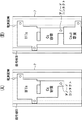
図3は、各画素回路2を構成する薄膜トランジスタTFT、画素容量Cs及び追加容量Csubのレイアウトを示す模式的な平面図である。(A)は追加容量Csubを形成しない場合を表しており、(B)は本発明にしたがって追加容量Csubを形成した場合を表している。サンプリングトランジスタTr1、ドライブトランジスタTrd及び補正手段(Tr2〜Tr4)は、絶縁基板上に形成された薄膜トランジスタTFTsからなり、画素容量Csと追加容量Csubは同じく絶縁基板上に形成された薄膜容量素子からなる。図示の例では、追加容量Csubの一方の端子はアノードコンタクトを介して画素容量Csに接続する一方、他方の端子は所定の固定電位に接続されている。この固定電位は、発光素子ELのカソード側になる接地電位Vcath、画素回路2の正側電源電位Vccまたは負側電源電位Vssなどから選択される。図2に示した実施形態では追加容量Csubの他方の端子は接地電位に接続されている。なお図3に示した画素回路2は積層構造となっており、下層にTFTs,Cs,Csubなどが形成されている。上層に発光素子ELが接続されている。理解を容易にするため、図3では上層の発光素子ELが除かれている。実際には、発光素子ELはアノードコンタクトを介して画素回路2側に接続することになる。
FIG. 3 is a schematic plan view showing a layout of the thin film transistor TFT, the pixel capacitor Cs, and the additional capacitor Csub constituting each
図4は、図2に示した表示装置から画素回路2の部分を取り出した模式図である。理解を容易にするためサンプリングトランジスタTr1によってサンプリングされる映像信号Vsigや、ドライブトランジスタTrdの入力電圧Vgs及び出力電流Ids、さらには発光素子ELが有する容量成分Coledや追加容量Csubなどを書き加えてある。以下図4に基づいて、本画素回路2の基本的な動作を説明する。
FIG. 4 is a schematic diagram in which a portion of the
図5は、図4に示した画素回路のタイミングチャートである。図5を参照して、図4に示した画素回路の動作をより具体的且つ詳細に説明する。図5は、時間軸Tに沿って各走査線WS,AZ1,AZ2及びDSに印加される制御信号の波形を表してある。表記を簡略化する為、制御信号も対応する走査線の符号と同じ符号で表してある。トランジスタTr1,Tr2,Tr3はNチャネル型なので、走査線WS,AZ1,AZ2がそれぞれハイレベルの時オンし、ローレベルの時オフする。一方トランジスタTr4はPチャネル型なので、走査線DSがハイレベルの時オフし、ローレベルの時オンする。なおこのタイミングチャートは、各制御信号WS,AZ1,AZ2,DSの波形と共に、ドライブトランジスタTrdのゲートGの電位変化及びソースSの電位変化も表してある。 FIG. 5 is a timing chart of the pixel circuit shown in FIG. With reference to FIG. 5, the operation of the pixel circuit shown in FIG. 4 will be described more specifically and in detail. FIG. 5 shows waveforms of control signals applied to the scanning lines WS, AZ1, AZ2, and DS along the time axis T. In order to simplify the notation, the control signals are also represented by the same reference numerals as the corresponding scanning lines. Since the transistors Tr1, Tr2 and Tr3 are N-channel type, they are turned on when the scanning lines WS, AZ1 and AZ2 are at a high level, and turned off when the scanning lines are at a low level. On the other hand, since the transistor Tr4 is a P-channel type, it is turned off when the scanning line DS is at a high level and turned on when it is at a low level. This timing chart also shows the change in the potential of the gate G and the change in the potential of the source S of the drive transistor Trd, along with the waveforms of the control signals WS, AZ1, AZ2, and DS.
図5のタイミングチャートではタイミングT1〜T8までを1フィールド(1f)としてある。1フィールドの間に画素アレイの各行が一回順次走査される。タイミングチャートは、1行分の画素に印加される各制御信号WS,AZ1,AZ2,DSの波形を表してある。 In the timing chart of FIG. 5, timings T1 to T8 are defined as one field (1f). Each row of the pixel array is sequentially scanned once during one field. The timing chart shows the waveforms of the control signals WS, AZ1, AZ2, DS applied to the pixels for one row.
当該フィールドが始まる前のタイミングT0で、全ての制御線号WS,AZ1,AZ2,DSがローレベルにある。したがってNチャネル型のトランジスタTr1,Tr2,Tr3はオフ状態にある一方、Pチャネル型のトランジスタTr4のみオン状態である。したがってドライブトランジスタTrdはオン状態のトランジスタTr4を介して電源Vccに接続しているので、所定の入力電圧Vgsに応じて出力電流Idsを発光素子ELに供給している。したがってタイミングT0で発光素子ELは発光している。この時ドライブトランジスタTrdに印加される入力電圧Vgsは、ゲート電位(G)とソース電位(S)の差で表される。 At timing T0 before the field starts, all control line numbers WS, AZ1, AZ2, DS are at a low level. Therefore, the N-channel transistors Tr1, Tr2, Tr3 are in the off state, while only the P-channel transistor Tr4 is in the on state. Therefore, since the drive transistor Trd is connected to the power supply Vcc via the transistor Tr4 in the on state, the output current Ids is supplied to the light emitting element EL according to the predetermined input voltage Vgs. Therefore, the light emitting element EL emits light at the timing T0. At this time, the input voltage Vgs applied to the drive transistor Trd is expressed by the difference between the gate potential (G) and the source potential (S).
当該フィールドが始まるタイミングT1で、制御信号DSがローレベルからハイレベルに切り替わる。これによりトランジスタTr4がオフし、ドライブトランジスタTrdは電源Vccから切り離されるので、発光が停止し非発光期間に入る。したがってタイミングT1に入ると、全てのトランジスタTr1〜Tr4がオフ状態になる。 At the timing T1 when the field starts, the control signal DS is switched from the low level to the high level. As a result, the transistor Tr4 is turned off and the drive transistor Trd is disconnected from the power supply Vcc, so that the light emission stops and the non-light emission period starts. Therefore, at the timing T1, all the transistors Tr1 to Tr4 are turned off.
続いてタイミングT2に進むと、制御信号AZ1及びAZ2がハイレベルになるので、スイッチングトランジスタTr2及びTr3がオンする。この結果、ドライブトランジスタTrdのゲートGが基準電位Vss1に接続し、ソースSが基準電位Vss2に接続される。ここでVss1−Vss2>Vthを満たしており、Vss1−Vss2=Vgs>Vthとする事で、その後タイミングT3で行われるVth補正の準備を行う。換言すると期間T2‐T3は、ドライブトランジスタTrdのリセット期間に相当する。また、発光素子ELの閾電圧をVthELとすると、VthEL>Vss2に設定されている。これにより、発光素子ELにはマイナスバイアスが印加され、いわゆる逆バイアス状態となる。この逆バイアス状態は、後で行うVth補正動作及び移動度補正動作を正常に行うために必要である。 Subsequently, at timing T2, since the control signals AZ1 and AZ2 are at a high level, the switching transistors Tr2 and Tr3 are turned on. As a result, the gate G of the drive transistor Trd is connected to the reference potential Vss1, and the source S is connected to the reference potential Vss2. Here, Vss1−Vss2> Vth is satisfied, and by setting Vss1−Vss2 = Vgs> Vth, preparation for Vth correction performed at timing T3 is performed. In other words, the period T2-T3 corresponds to a reset period of the drive transistor Trd. Further, when the threshold voltage of the light emitting element EL is VthEL, VthEL> Vss2 is set. Thereby, a minus bias is applied to the light emitting element EL, and a so-called reverse bias state is obtained. This reverse bias state is necessary for normally performing the Vth correction operation and the mobility correction operation to be performed later.
タイミングT3では制御信号AZ2をローレベルにし且つ直後制御信号DSもローレベルにしている。これによりトランジスタTr3がオフする一方トランジスタTr4がオンする。この結果ドレイン電流Idsが画素容量Csに流れ込み、Vth補正動作を開始する。この時ドライブトランジスタTrdのゲートGはVss1に保持されており、ドライブトランジスタTrdがカットオフするまで電流Idsが流れる。カットオフするとドライブトランジスタTrdのソース電位(S)はVss1−Vthとなる。ドレイン電流がカットオフした後のタイミングT4で制御信号DSを再びハイレベルに戻し、スイッチングトランジスタTr4をオフする。さらに制御信号AZ1もローレベルに戻し、スイッチングトランジスタTr2もオフする。この結果、画素容量CsにVthが保持固定される。この様にタイミングT3‐T4はドライブトランジスタTrdの閾電圧Vthを検出する期間である。ここでは、この検出期間T3‐T4をVth補正期間と呼んでいる。 At timing T3, the control signal AZ2 is set to the low level, and the control signal DS is also set to the low level. As a result, the transistor Tr3 is turned off while the transistor Tr4 is turned on. As a result, the drain current Ids flows into the pixel capacitor Cs, and the Vth correction operation is started. At this time, the gate G of the drive transistor Trd is held at Vss1, and the current Ids flows until the drive transistor Trd is cut off. When cut off, the source potential (S) of the drive transistor Trd becomes Vss1-Vth. At timing T4 after the drain current is cut off, the control signal DS is returned to the high level again, and the switching transistor Tr4 is turned off. Further, the control signal AZ1 is also returned to the low level, and the switching transistor Tr2 is also turned off. As a result, Vth is held and fixed in the pixel capacitor Cs. Thus, the timing T3-T4 is a period for detecting the threshold voltage Vth of the drive transistor Trd. Here, this detection period T3-T4 is called a Vth correction period.
この様にVth補正を行った後タイミングT5で制御信号WSをハイレベルに切り替え、サンプリングトランジスタTr1をオンして映像信号Vsigを画素容量Csに書き込む。発光素子ELの等価容量Coledに比べて画素容量Csは充分に小さい。この結果、映像信号Vsigのほとんど大部分が画素容量Csに書き込まれる。正確には、Vss1に対する。Vsigの差分Vsig−Vss1が画素容量Csに書き込まれる。したがってドライブトランジスタTrdのゲートGとソースS間の電圧Vgsは、先に検出保持されたVthと今回サンプリングされたVsig−Vss1を加えたレベル(Vsig−Vss1+Vth)となる。以降説明簡易化の為Vss1=0Vとすると、ゲート/ソース間電圧Vgsは図5のタイミングチャートに示すようにVsig+Vthとなる。かかる映像信号Vsigのサンプリングは制御信号WSがローレベルに戻るタイミングT7まで行われる。すなわちタイミングT5‐T7がサンプリング期間に相当する。 After performing the Vth correction in this way, the control signal WS is switched to the high level at timing T5, the sampling transistor Tr1 is turned on, and the video signal Vsig is written into the pixel capacitor Cs. The pixel capacitance Cs is sufficiently smaller than the equivalent capacitance Coled of the light emitting element EL. As a result, most of the video signal Vsig is written into the pixel capacitor Cs. To be precise, for Vss1. The difference Vsig−Vss1 of Vsig is written to the pixel capacitor Cs. Therefore, the voltage Vgs between the gate G and the source S of the drive transistor Trd becomes a level (Vsig−Vss1 + Vth) obtained by adding Vth previously detected and held and Vsig−Vss1 sampled this time. Hereinafter, if Vss1 = 0V for simplification of description, the gate / source voltage Vgs becomes Vsig + Vth as shown in the timing chart of FIG. The sampling of the video signal Vsig is performed until timing T7 when the control signal WS returns to the low level. That is, the timing T5-T7 corresponds to the sampling period.
サンプリング期間の終了するタイミングT7より前のタイミングT6で制御信号DSがローレベルとなりスイッチングトランジスタTr4がオンする。これによりドライブトランジスタTrdが電源Vccに接続されるので、画素回路は非発光期間から発光期間に進む。この様にサンプリングトランジスタTr1がまだオン状態で且つスイッチングトランジスタTr4がオン状態に入った期間T6‐T7で、ドライブトランジスタTrdの移動度補正を行う。即ち本実施形態では、サンプリング期間の後部分と発光期間の先頭部分とが重なる期間T6‐T7で移動度補正を行っている。なお、この移動度補正を行う発光期間の先頭では、発光素子ELは実際には逆バイアス状態にあるので発光する事はない。この移動度補正期間T6‐T7では、ドライブトランジスタTrdのゲートGが映像信号Vsigのレベルに固定された状態で、ドライブトランジスタTrdにドレイン電流Idsが流れる。ここでVss1−Vth<VthELと設定しておく事で、発光素子ELは逆バイアス状態におかれる為、ダイオード特性ではなく単純な容量特性を示すようになる。よってドライブトランジスタTrdに流れる電流Idsは画素容量Csと発光素子ELの等価容量Coledと追加容量Csubの三者を結合した容量C=Cs+Coled+Csubに書き込まれていく。これによりドライブトランジスタTrdのソース電位(S)は上昇していく。図5のタイミングチャートではこの上昇分をΔVで表してある。この上昇分ΔVは結局画素容量Csに保持されたゲート/ソース間電圧Vgsから差し引かれる事になるので、負帰還をかけた事になる。この様にドライブトランジスタTrdの出力電流Idsを同じくドライブトランジスタTrdの入力電圧Vgsに負帰還する事で、移動度μを補正する事が可能である。なお負帰還量ΔVは移動度補正期間T6‐T7の時間幅tを調整する事で最適化可能である。 At timing T6 before the end of the sampling period T7, the control signal DS becomes low level and the switching transistor Tr4 is turned on. As a result, the drive transistor Trd is connected to the power supply Vcc, so that the pixel circuit proceeds from the non-light emitting period to the light emitting period. In this manner, the mobility correction of the drive transistor Trd is performed in the period T6-T7 in which the sampling transistor Tr1 is still on and the switching transistor Tr4 is on. That is, in the present embodiment, the mobility correction is performed in the period T6-T7 in which the latter part of the sampling period and the head part of the light emission period overlap. Note that, at the beginning of the light emission period in which the mobility correction is performed, the light emitting element EL is actually in a reverse bias state, and thus does not emit light. In the mobility correction period T6-T7, the drain current Ids flows through the drive transistor Trd while the gate G of the drive transistor Trd is fixed at the level of the video signal Vsig. Here, by setting Vss1−Vth <VthEL, the light emitting element EL is placed in a reverse bias state, so that it exhibits simple capacitance characteristics instead of diode characteristics. Therefore, the current Ids flowing through the drive transistor Trd is written in a capacitor C = Cs + Coled + Csub that combines the pixel capacitor Cs, the equivalent capacitor Coled of the light emitting element EL, and the additional capacitor Csub. As a result, the source potential (S) of the drive transistor Trd increases. In the timing chart of FIG. 5, this increase is represented by ΔV. Since this increase ΔV is eventually subtracted from the gate / source voltage Vgs held in the pixel capacitor Cs, negative feedback is applied. In this way, the mobility μ can be corrected by negatively feeding back the output current Ids of the drive transistor Trd to the input voltage Vgs of the drive transistor Trd. The negative feedback amount ΔV can be optimized by adjusting the time width t of the mobility correction period T6-T7.
タイミングT7では制御信号WSがローレベルとなりサンプリングトランジスタTr1がオフする。この結果ドライブトランジスタTrdのゲートGは信号線SLから切り離される。映像信号Vsigの印加が解除されるので、ドライブトランジスタTrdのゲート電位(G)は上昇可能となり、ソース電位(S)と共に上昇していく。その間画素容量Csに保持されたゲート/ソース間電圧Vgsは(Vsig−ΔV+Vth)の値を維持する。ソース電位(S)の上昇に伴い、発光素子ELの逆バイアス状態は解消されるので、出力電流Idsの流入により発光素子ELは実際に発光を開始する。この時のドレイン電流Ids対ゲート電圧Vgsの関係は、先のトランジスタ特性式1のVgsにVsig−ΔV+Vthを代入する事で、以下の式2のように与えられる。
Ids=kμ(Vgs−Vth)2=kμ(Vsig−ΔV)2・・・式2
上記式2において、k=(1/2)(W/L)Coxである。この特性式2からVthの項がキャンセルされており、発光素子ELに供給される出力電流IdsはドライブトランジスタTrdの閾電圧Vthに依存しない事が分かる。基本的にドレイン電流Idsは映像信号の信号電圧Vsigによって決まる。換言すると、発光素子ELは映像信号Vsigに応じた輝度で発光する事になる。その際Vsigは帰還量ΔVで補正されている。この補正量ΔVは丁度特性式2の係数部に位置する移動度μの効果を打ち消すように働く。したがって、ドレイン電流Idsは実質的に映像信号Vsigのみに依存する事になる。
At timing T7, the control signal WS becomes low level and the sampling transistor Tr1 is turned off. As a result, the gate G of the drive transistor Trd is disconnected from the signal line SL. Since the application of the video signal Vsig is cancelled, the gate potential (G) of the drive transistor Trd can be increased and increases with the source potential (S). Meanwhile, the gate / source voltage Vgs held in the pixel capacitor Cs maintains a value of (Vsig−ΔV + Vth). As the source potential (S) rises, the reverse bias state of the light emitting element EL is canceled, so that the light emitting element EL actually starts to emit light by the inflow of the output current Ids. The relationship between the drain current Ids and the gate voltage Vgs at this time is given by the
Ids = kμ (Vgs−Vth) 2 = kμ (Vsig−ΔV) 2
In the
最後にタイミングT8に至ると制御信号DSがハイレベルとなってスイッチングトランジスタTr4がオフし、発光が終了すると共に当該フィールドが終わる。この後次のフィールドに移って再びVth補正動作、移動度補正動作及び発光動作が繰り返される事になる。 Finally, when the timing T8 is reached, the control signal DS becomes high level, the switching transistor Tr4 is turned off, the light emission ends, and the field ends. Thereafter, the operation proceeds to the next field, and the Vth correction operation, the mobility correction operation, and the light emission operation are repeated again.
図6は、移動度補正期間T6‐T7における画素回路2の状態を示す回路図である。図示するように、移動度補正期間T6‐T7では、サンプリングトランジスタTr1及びスイッチングトランジスタTr4がオンしている一方、残りのスイッチングトランジスタTr2及びTr3がオフしている。この状態でドライブトランジスタTr4のソース電位(S)はVss1−Vthである。このソース電位Sは発光素子ELのアノード電位でもある。前述したようにVss1−Vth<VthELと設定しておく事で、発光素子ELは逆バイアス状態におかれ、ダイオード特性ではなく単純な容量特性を示す事になる。よってドライブトランジスタTrdに流れる電流Idsは画素容量Csと発光素子ELの等価容量Coledと追加容量Csubとの合成容量C=Cs+Coled+Csubに流れ込む事になる。換言すると、ドレイン電流Idsの一部が画素容量Csに負帰還され、移動度の補正が行われる。
FIG. 6 is a circuit diagram illustrating a state of the
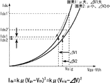
図7は上述したトランジスタ特性式2をグラフ化したものであり、縦軸にIdsを取り横軸にVsigを取ってある。このグラフの下方に特性式2も合わせて示してある。図7のグラフは、画素1と画素2を比較した状態で特性カーブを描いてある。画素1のドライブトランジスタの移動度μは相対的に大きい。逆に画素2に含まれるドライブトランジスタの移動度μは相対的に小さい。この様にドライブトランジスタをポリシリコン薄膜トランジスタなどで構成した場合、画素間で移動度μがばらつく事は避けられない。例えば両画素1,2に同レベルの映像信号Vsigを書き込んだ場合、何ら移動度の補正を行わないと、移動度μの大きい画素1に流れる出力電流Ids1´は、移動度μの小さい画素2に流れる出力電流Ids2´に比べて大きな差が生じてしまう。この様に移動度μのばらつきに起因して出力電流Idsの間に大きな差が生じるので、画面のユニフォーミティを損なう事になる。
FIG. 7 is a graph of the above-described transistor
そこで本発明では出力電流を入力電圧側に負帰還させる事で移動度のばらつきをキャンセルしている。トランジスタ特性式から明らかなように、移動度が大きいとドレイン電流Idsが大きくなる。したがって負帰還量ΔVは移動度が大きいほど大きくなる。図7のグラフに示すように、移動度μの大きな画素1の負帰還量ΔV1は移動度の小さな画素2の負帰還量ΔV2に比べて大きい。したがって、移動度μが大きいほど負帰還が大きくかかる事となって、ばらつきを抑制する事が可能である。図示するように、移動度μの大きな画素1でΔV1の補正をかけると、出力電流はIds1´からIds1まで大きく下降する。一方移動度μの小さな画素2の補正量ΔV2は小さいので、出力電流Ids2´はIds2までそれ程大きく下降しない。結果的に、Ids1とIds2は略等しくなり、移動度のばらつきがキャンセルされる。この移動度のばらつきのキャンセルは黒レベルから白レベルまでVsigの全範囲で行われるので、画面のユニフォーミティは極めて高くなる。以上をまとめると、移動度の異なる画素1と2があった場合、移動度の大きい画素1の補正量ΔV1は移動度の小さい画素2の補正量ΔV2に対して小さくなる。つまり移動度が大きいほどΔVが大きくIdsの減少値は大きくなる。これにより移動度の異なる画素電流値は均一化され、移動度のばらつきを補正する事ができる。
Therefore, in the present invention, the variation in mobility is canceled by negatively feeding back the output current to the input voltage side. As is clear from the transistor characteristic equation, the drain current Ids increases when the mobility is large. Therefore, the negative feedback amount ΔV increases as the mobility increases. As shown in the graph of FIG. 7, the negative feedback amount ΔV1 of the
以下図8を参照して、上述した移動度補正の数値解析を行う。図8に示すように、トランジスタTr1及びTr4がオンした状態で、ドライブトランジスタTrdのソース電位を変数Vに取って解析を行う。ドライブトランジスタTrdのソース電位(S)をVとすると、ドライブトランジスタTrdを流れるドレイン電流Idsは以下の式3に示す通りである。
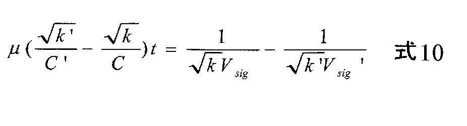
またドレイン電流Idsと容量C(=Cs+Coled+Csub)の関係により、以下の式4に示す様にIds=dQ/dt=CdV/dtが成り立つ。
式4に式3を代入して両辺積分する。ここで、ソース電圧V初期状態は−Vthであり、移動度ばらつき補正時間(T6‐T7)をtとする。この微分方程式を解くと、移動度補正時間tに対する画素電流が以下の数式5のように与えられる。
図9は、式5をグラフ化した図であり、縦軸に出力電流Idsを取り、横軸に映像信号Vsigを取ってある。パレメータとして移動度補正期間t=0us、2.5us及び5usの場合を設定している。さらに、移動度μもパラメータとして比較的大きい場合1.2μと比較的小さい場合0.8μをパラメータにとってある。加えて、CはCs+ColedのみでCsubは0としている。t=0usとして実質的に移動度補正をかけない場合に比べ、t=2.5usでは移動度ばらつきに対する補正が十分にかかっていることがわかる。移動度補正なしではIdsに40%のばらつきがあったものが、移動度補正をかけると10%以下に抑えられる。但しt=5usとして補正期間を長くすると逆に移動度μの違いによる出力電流Idsのばらつきが大きくなってしまう。この様に、適切な移動度補正を掛けるために、tは最適な値に設定する必要がある。図9に示したグラフの場合、最適値はt=2.5usの近辺である。しかしながら、トランジスタのゲートに印加される制御信号(ゲートパルス)の遅延などを考えると、t=2.5usは必ずしも妥当ではなく、トランジスタの動作特性から考えると、tはより長いほうが良い。ここで前述の式5を見ると、tはt/Cとして式中に含まれていることが分かる。したがって、式5の右辺に影響を与えることなくtを大きくする為には、t/Cの値を一定に保ちつつ、Cの値を大きくすれば良いことになる。このため、本発明では容量Cを構成する画素容量Csと発光素子容量Coledに加え追加容量Csubを画素回路中に導入している。このCsubを加えることでトータル容量Cの値が大きくなり、その分tも延長でき、画素回路に含まれる補正手段の時間的な動作マージンを広げることが可能になる。
FIG. 9 is a graph of
以上説明したように、移動度補正期間においては、図5のタイミングチャートに示したとおり、ゲート電位を固定して状態でドライブトランジスタTrdに出力電流Idsを流し、画素容量Csや発光素子容量Coledに電荷を書き込む。その出力電流Idsの値は式5に示した通りであり、Vthの項を含まずしたがってVthの影響を受けることなく移動度の補正を行える。即ち、式5の右辺の分母に移動度μを含む項を有しており、移動度μが大きい場合は出力電流Idsが小さくなり、逆に移動度μが小さい場合は出力電流Idsが大きくなることで、移動度ばらつきの補正が行われる。
As described above, in the mobility correction period, as shown in the timing chart of FIG. 5, the output current Ids is supplied to the drive transistor Trd with the gate potential fixed, and the pixel capacitance Cs and the light emitting element capacitance Coled are supplied. Write a charge. The value of the output current Ids is as shown in
式5の移動度補正項ではt/Cを含んでいる。tは前述したように移動度補正時間であり、Cは画素容量Csや発光素子容量Coledなどの合成容量からなる。ここで移動度補正時間tと出力電流をばらつきの関係は図9のグラフに示した通りである。前述したように、移動度補正時間tは短すぎても、長すぎても補正効果が不十分になることがわかっている。図9のグラフでは例えばt=2.5usが略最適レベルである。一方でゲートパルスの遅延などを考えるとt=2.5usは短すぎる場合が多く、移動度補正時間tを正確にコントロールすることは事実上困難である。
The mobility correction term in
そこで本発明では、前述の移動度補正調整を容易にするため、移動度補正に用いられる容量Cを増加させている。容量Cを増加させるためには、発光素子容量Coledまたは画素容量Csを大きくするか、あるいは追加容量Csubを設けることが考えられる。ここで発光素子容量Coledは、画素サイズと画素開口率に加えて発光素子を構成する有機EL材料などの基本特性により決定され、単純に増加させることは容易ではない。また画素容量Csを増加させてしまうと、信号電圧書き込み時にアノード電位の上昇が大きくなる。具体的には、アノード電位の上昇分はCs/(Cs+Coled)×ΔVにて決定される。したがってColed/(Cs+Coled)で表される入力信号電圧ゲインが低下してしまう。この入力電圧ゲインの低下を補うためには映像信号の振幅レベルを大きくしなければならず、その分ドライバ側に負担がかかる。そこで本発明では、容量Cを増加させる為に、TFTが集積形成されている絶縁基板上に追加容量Csubを形成し、これをColedと並列に接続する。これにより、入力ゲイン(Coled+Csub)/(Cs+Coled+Csub)を上げながら、トータル容量Cの値を大きくすることができ、最適な移動度補正時間tを長く設定することができるようになり、移動度補正時間設定のマージンを上げることができる。なお第1実施形態の画素回路ではドライブトランジスタTrdをNチャネル型とし、これ以外のスイッチングトランジスタはNチャネル型とPチャネル型を混在して用いているが、各トランジスタの特性はNチャネルでもPチャネルでもかまわない。 Therefore, in the present invention, the capacity C used for mobility correction is increased in order to facilitate the above-described mobility correction adjustment. In order to increase the capacitance C, it is conceivable to increase the light emitting element capacitance Coled or the pixel capacitance Cs, or to provide an additional capacitance Csub. Here, the light emitting element capacitance Coled is determined by basic characteristics such as an organic EL material constituting the light emitting element in addition to the pixel size and the pixel aperture ratio, and it is not easy to increase it simply. Also, if the pixel capacitance Cs is increased, the anode potential increases greatly when the signal voltage is written. Specifically, the increase in anode potential is determined by Cs / (Cs + Coled) × ΔV. Therefore, the input signal voltage gain represented by Coled / (Cs + Coled) is reduced. In order to compensate for the decrease in the input voltage gain, the amplitude level of the video signal has to be increased, which places a burden on the driver side. Therefore, in the present invention, in order to increase the capacitance C, an additional capacitance Csub is formed on an insulating substrate on which TFTs are integrally formed, and this is connected in parallel with Coled. As a result, the value of the total capacitance C can be increased while increasing the input gain (Coled + Csub) / (Cs + Coled + Csub), and the optimum mobility correction time t can be set longer, and the mobility correction time is increased. The setting margin can be increased. In the pixel circuit of the first embodiment, the drive transistor Trd is an N-channel type, and other switching transistors are used in a mixture of an N-channel type and a P-channel type. But it doesn't matter.
図10は、図2に示した第1実施形態の変形例を示す回路図である。第1実施形態の場合、追加容量Csubの一方の端子は発光素子ELのアノードに接続し、他方の端子は発光素子ELのカソード側と同じ接地電位Vcathに接続されている。これに対し本変形例は追加容量Csubの他方の端子が電源電位Vccに接続されている。この様に本発明は追加容量Csubの他方の端子が固定電位に接続されていれば良い。この固定電位は、発光素子ELのカソード側になる接地電位Vcath、画素回路2の正側電源電位Vccまたは負側電源電位から適宜選択することが出来る。場合によっては、追加容量Csubを画素容量Csと並列に作成しても、トータル容量Cを増加することが出来る。しかしながらこの場合は前述したように画素容量Csと追加容量Csubを並列に接続することで入力信号のゲインが低下してしまう。したがって画素容量Csと並列に追加容量Csubを接続しない方が望ましい。
FIG. 10 is a circuit diagram showing a modification of the first embodiment shown in FIG. In the first embodiment, one terminal of the additional capacitor Csub is connected to the anode of the light emitting element EL, and the other terminal is connected to the same ground potential Vcath as the cathode side of the light emitting element EL. On the other hand, in the present modification, the other terminal of the additional capacitor Csub is connected to the power supply potential Vcc. In this way, in the present invention, it is only necessary that the other terminal of the additional capacitor Csub is connected to a fixed potential. This fixed potential can be appropriately selected from the ground potential Vcath on the cathode side of the light emitting element EL, the positive power supply potential Vcc or the negative power supply potential of the
図11は、本発明にかかる表示装置の第2実施形態を示すブロック図である。理解を容易にするため図2に示した第1実施形態と対応する部分には対応する参照番号を用いてある。本表示装置は、画素アレイ1とこれを囲む周辺の回路とで構成されている。周辺回路は、水平セレクタ3とライトスキャナ4とドライブスキャナ5と第一補正用スキャナ71と第二補正用スキャナ72とを含む。画素アレイ1はマトリクス状に配列した画素回路2で構成されている。図では理解を容易にする為1個の画素回路2のみを示してある。画素回路2は6個のトランジスタTr1,Trd,Tr3〜Tr6と、3個の容量素子Cs1,Cs2,Csubと1個の発光素子ELとで構成されている。トランジスタは全てNチャネル型である。本画素回路2の主要部となるドライブトランジスタTrdは、そのゲートGが各容量素子Cs1,Cs2の一端に接続されている。一方の容量素子Cs1は本画素回路2の出力側と入力側を結ぶ結合容量である。他方の容量素子Cs2は結合容量Cs1を介して映像信号が書き込まれる画素容量である。ドライブトランジスタTrdのソースSは画素容量Cs2の他端に接続すると共に、発光素子ELに接続している。発光素子ELはダイオード型のデバイスであり、そのアノードがドライブトランジスタTrdのソースSに接続する一方、カソードKが接地電位Vcathに接続されている。容量素子Csubは本発明に従って追加した追加容量であり、ドライブトランジスタTrdのソースSと接地電位Vcathとの間に接続されている。またドライブトランジスタTrdのソースSと所定の基準電位Vss2との間にスイッチングトランジスタTr3が介在している。このトランジスタTr3のゲートは走査線AZ2に接続している。ドライブトランジスタTrdのドレインはスイッチングトランジスタTr4を介して電源Vccに接続されている。スイッチングトランジスタTr4のゲートは走査線DSに接続している。加えてドライブトランジスタTrdのゲートGとドレインとの間にスイッチングトランジスタTr5が介在している。このトランジスタTr5のゲートは走査線AZ1に接続している。一方入力側のサンプリングトランジスタTr1は信号線SLと結合容量Cs1の他端との間に接続されている。サンプリングトランジスタTr1のゲートは走査線WSに接続されている。結合容量Cs1の他端と所定の基準電位Vss1との間にトランジスタTr6が介在している。このトランジスタTr6のゲートは走査線AZ1に接続している。
FIG. 11 is a block diagram showing a second embodiment of the display device according to the present invention. For easy understanding, the same reference numerals are used for the portions corresponding to the first embodiment shown in FIG. The display device includes a
図12は、図11に示した画素回路の動作説明に供するタイミングチャートである。時間軸Tに沿って制御信号WS,DS,AZ1,AZ2の波形を表すと共に、ドライブトランジスタTrdのゲート電位(G)及びソース電位(S)の変化も表してある。当該フィールドが開始するタイミングT1では、制御信号WS,AZ1,AZ2がローレベルで、制御信号DSのみがハイレベルである。したがって、タイミングT1ではスイッチングトランジスタTr4のみがオン状態にあり、残りのトランジスタTr1,Tr3,Tr5,Tr6はオフ状態にある。この時ドライブトランジスタTrdはオン状態にあるスイッチングトランジスタTr4を介して電源Vccに接続されているので、所定のドレイン電流Idsが発光素子ELに流れる為、発光状態となっている。 FIG. 12 is a timing chart for explaining the operation of the pixel circuit shown in FIG. Along with the time axis T, the waveforms of the control signals WS, DS, AZ1, and AZ2 are shown, and changes in the gate potential (G) and the source potential (S) of the drive transistor Trd are also shown. At timing T1 when the field starts, the control signals WS, AZ1, and AZ2 are at a low level, and only the control signal DS is at a high level. Therefore, at the timing T1, only the switching transistor Tr4 is in the on state, and the remaining transistors Tr1, Tr3, Tr5, Tr6 are in the off state. At this time, since the drive transistor Trd is connected to the power supply Vcc via the switching transistor Tr4 in the on state, the predetermined drain current Ids flows through the light emitting element EL, and thus the light emitting state is obtained.
タイミングT2になると制御信号AZ1とAZ2とがハイレベルとなり、スイッチングトランジスタTr5,Tr6がオンする。ドライブトランジスタTrdのゲートGはトランジスタTr5を通して電源Vcc側に接続するので、ゲート電位(G)は急激に上昇する。 At timing T2, the control signals AZ1 and AZ2 become high level, and the switching transistors Tr5 and Tr6 are turned on. Since the gate G of the drive transistor Trd is connected to the power supply Vcc side through the transistor Tr5, the gate potential (G) rises rapidly.
この後タイミングT3で制御信号DSがローレベルとなり、トランジスタTr4がオフする。ドライブトランジスタTrdに対する電源供給が遮断されるので、ドレイン電流Idsは減衰していく。これによりソース電位(S)及びゲート電位(G)は共に下降するが、丁度両者の電位差がVthとなったところで電流が流れなくなる。この時のVthが画素容量Cs2に保持される。画素容量Cs2に保持されたVthはドライブトランジスタTrdの閾電圧のキャンセルに用いられる。また、スイッチングトランジスタTr3はオンしており、ドライブトランジスタTr2のソースSはトランジスタTr3を介して基準電位Vss2に接続される。このVss2は発光素子ELの閾電圧よりも低く設定されており、発光素子ELは逆バイアス状態におかれる。 Thereafter, at timing T3, the control signal DS becomes low level, and the transistor Tr4 is turned off. Since the power supply to the drive transistor Trd is cut off, the drain current Ids attenuates. As a result, both the source potential (S) and the gate potential (G) drop, but the current stops flowing when the potential difference between the two becomes Vth. At this time, Vth is held in the pixel capacitor Cs2. Vth held in the pixel capacitor Cs2 is used to cancel the threshold voltage of the drive transistor Trd. Further, the switching transistor Tr3 is on, and the source S of the drive transistor Tr2 is connected to the reference potential Vss2 via the transistor Tr3. This Vss2 is set lower than the threshold voltage of the light emitting element EL, and the light emitting element EL is put in a reverse bias state.
この後タイミングT4になったとき制御信号AZ1がローレベルとなり、トランジスタTr5,Tr6がオフして、Cs2に書き込まれたVthが固定される。タイミングT2からT4までVth補正期間(T2‐T4)と呼ぶ。なおVth補正期間ではTr6がオンしている為、結合容量Cs1の他端は所定の基準電位Vss1に保持される。 Thereafter, at timing T4, the control signal AZ1 becomes low level, the transistors Tr5 and Tr6 are turned off, and Vth written to Cs2 is fixed. From timing T2 to T4 is referred to as a Vth correction period (T2-T4). Since Tr6 is on during the Vth correction period, the other end of the coupling capacitor Cs1 is held at a predetermined reference potential Vss1.
タイミングT5になると制御信号WS及びAZ2がハイレベルになり、サンプリングトランジスタTr1がオンする。この結果、ドライブトランジスタTrdのゲートGは結合容量Cs1及びオンしたサンプリングトランジスタTr1を介して信号線SLに接続される。この結果映像信号が結合容量Cs1を介してドライブトランジスタTrdのゲートGにカップリングされ、その電位が上昇する。図13のタイミングチャートでは映像信号のカップリング分とVthを合わせた電圧をVinで表してある。画素容量Cs2にこのVinが保持された事になる。この後タイミングT7で制御信号WSがローレベルに戻り、画素容量Cs2に書き込まれた電位が保持固定される。この様にして映像信号が結合容量Cs1を介して画素容量Cs2に書き込まれる期間をサンプリング期間T5‐T7と呼ぶ。このサンプリング期間T5‐T7は通常1水平期間(1H)に相当する。 At timing T5, the control signals WS and AZ2 become high level, and the sampling transistor Tr1 is turned on. As a result, the gate G of the drive transistor Trd is connected to the signal line SL via the coupling capacitor Cs1 and the turned-on sampling transistor Tr1. As a result, the video signal is coupled to the gate G of the drive transistor Trd via the coupling capacitor Cs1, and its potential rises. In the timing chart of FIG. 13, the voltage obtained by combining the video signal coupling amount and Vth is represented by Vin. This Vin is held in the pixel capacitor Cs2. Thereafter, at timing T7, the control signal WS returns to the low level, and the potential written in the pixel capacitor Cs2 is held and fixed. A period in which the video signal is written to the pixel capacitor Cs2 through the coupling capacitor Cs1 in this way is called a sampling period T5-T7. This sampling period T5-T7 normally corresponds to one horizontal period (1H).
本実施形態では、サンプリング期間が終了するタイミングT7の前のタイミングT6で、制御信号DSがハイレベルになる一方制御信号AZ2がローレベルになる。この結果ドライブトランジスタTrdのソースSがVss2から切り離される一方ドレイン側からソースS側に向かって電流が流れる。一方サンプリングトランジスタTr1は引き続きオン状態なのでドライブトランジスタTrdのゲート電位(G)は映像信号側に保持されている。この様な状態でドライブトランジスタTrdに出力電流が流れるので、画素容量Cs2及び逆バイアス状態にある発光素子ELの等価容量を充電する事になる。これによりドライブトランジスタTrdのソース電位(S)はΔVだけ上昇し、その分だけCs2に保持されていた電圧Vinが減少する。換言すると、期間T6‐T7の間でソースS側の出力電流がゲートG側の入力電圧に負帰還される。この負帰還量がΔVで表される。この負帰還動作により、ドライブトランジスタTrdの移動度補正が行われる。 In the present embodiment, at timing T6 before timing T7 when the sampling period ends, the control signal DS becomes high level while the control signal AZ2 becomes low level. As a result, the source S of the drive transistor Trd is disconnected from Vss2, and a current flows from the drain side toward the source S side. On the other hand, since the sampling transistor Tr1 is still on, the gate potential (G) of the drive transistor Trd is held on the video signal side. Since an output current flows through the drive transistor Trd in such a state, the pixel capacitor Cs2 and the equivalent capacitor of the light emitting element EL in the reverse bias state are charged. As a result, the source potential (S) of the drive transistor Trd rises by ΔV, and the voltage Vin held in Cs2 decreases accordingly. In other words, the output current on the source S side is negatively fed back to the input voltage on the gate G side during the period T6-T7. This negative feedback amount is represented by ΔV. The mobility of the drive transistor Trd is corrected by this negative feedback operation.
この後タイミングT7で制御信号WSがローレベルとなり、映像信号の印加が解除されると、いわゆるブートストラップ動作が行われゲート電位(G)及びソース電位(S)は両者の差(Vin−ΔV)を維持したまま上昇する。ソース電位(S)の上昇に伴い発光素子ELの逆バイアス状態は解消されるので、出力電流Idsが発光素子ELに流れ込み、映像信号に応じた輝度で発光が行われる。この後タイミングT8で当該フィールド1fが終わると次のフィールドに進む。次のフィールドでも、Vth補正、信号書き込み、移動度補正の各動作を行う。
Thereafter, when the control signal WS becomes low level at the timing T7 and the application of the video signal is released, a so-called bootstrap operation is performed, and the difference between the gate potential (G) and the source potential (S) (Vin−ΔV). Ascending while maintaining. As the source potential (S) rises, the reverse bias state of the light-emitting element EL is canceled, so that the output current Ids flows into the light-emitting element EL, and light emission is performed with luminance corresponding to the video signal. Thereafter, when the
図13は、図12に示した移動度補正期間T6‐T7における画素回路2の状態を表している。この画素回路2もスイッチングトランジスタTr3,Tr4,Tr5などで構成される補正手段を備えている。この補正手段は出力電流Idsのキャリア移動度μに対する依存性を打ち消す為、予め発光期間T6‐T8の前または先頭で画素容量Cs2に保持された入力電圧Vin(Vgs)を補正する。この補正手段は走査線WS及びDSから供給される制御信号WS,DSに応じてサンプリング期間T5‐T7の一部で動作し、映像信号Vsigがサンプリングされている状態でドライブトランジスタTrdから出力電流Idsを取り出し、これを画素容量Cs2に負帰還して入力電圧Vgsを補正する。加えてこの補正手段(Tr3,Tr4,Tr5)は、出力電流Idsの閾電圧Vthに対する依存性を打ち消す為に、予めサンプリング期間T5‐T7に先立つ期間T2‐T4でドライブトランジスタTrdの閾電圧Vthを検出し、且つ検出された閾電圧Vthを入力電圧Vgsに足し込む様にしてある。
FIG. 13 shows the state of the
本実施形態においても、ドライブトランジスタTrdはNチャネル型トランジスタでドレインが電源Vcc側に接続する一方ソースSが発光素子EL側に接続している。この構成において本補正手段は、サンプリング期間T5‐T7の後部分に重なる発光期間T6‐T8の先頭部分(T6‐T7)でドライブトランジスタTrdから出力電流Idsを取り出して、画素容量Cs2側に負帰還する。その際本補正手段は、発光期間の先頭部分(T6‐T7)でドライブトランジスタTrdのソースS側から取り出した出力電流Idsが、発光素子ELの有する等価容量Coledと追加容量Csubに流れ込むようにしている。発光素子ELはアノード及びカソードを備えたダイオード型の発光素子からなり、アノード側がドライブトランジスタTrdのソースSに接続する一方カソード側がVcathに接地されている。本補正手段は前述したように予め発光素子ELのアノード/カソード間を逆バイアス状態にセットしておき、ドライブトランジスタTrdのソースS側から取り出した出力電流Idsが発光素子ELに流れ込む時、ダイオード型の発光素子ELを容量性素子Coledとして機能させている。その際発光素子容量Coledに追加容量Csubを接続してある。これにより出力電流Idsを流す時間を延長化でき、結果として移動度補正手段の時間的な動作マージンを拡大できる。 Also in this embodiment, the drive transistor Trd is an N-channel transistor, and the drain is connected to the power supply Vcc side while the source S is connected to the light emitting element EL side. In this configuration, the correction means takes out the output current Ids from the drive transistor Trd at the head part (T6-T7) of the light emission period T6-T8 that overlaps the rear part of the sampling period T5-T7, and negatively feeds back to the pixel capacitor Cs2 side. To do. At this time, the correction means causes the output current Ids extracted from the source S side of the drive transistor Trd at the head portion (T6-T7) of the light emission period to flow into the equivalent capacitance Coled and the additional capacitance Csub of the light emitting element EL. Yes. The light emitting element EL is composed of a diode type light emitting element having an anode and a cathode. The anode side is connected to the source S of the drive transistor Trd, and the cathode side is grounded to Vcath. As described above, the correction means sets the anode / cathode of the light emitting element EL in a reverse bias state in advance, and when the output current Ids extracted from the source S side of the drive transistor Trd flows into the light emitting element EL, the diode type The light emitting element EL is made to function as the capacitive element Coled. At this time, an additional capacitor Csub is connected to the light emitting element capacitor Coled. As a result, the time during which the output current Ids is passed can be extended, and as a result, the temporal operation margin of the mobility correction means can be expanded.
図14は、本発明にかかる表示装置の第3実施形態を示す模式的な平面図である。図14は1セット分の赤色画素、緑色画素及び青色画素の模式的な平面図である。RGB各色の画素回路2は、各々赤色発光素子、緑色発光素子及び青色発光素子を備えている。各画素回路2に形成された追加容量Csubは、各色発光素子毎に異なる容量値を有し、以ってRGB各画素回路に形成された各補正手段の動作に要する時間を均一化している。
FIG. 14 is a schematic plan view showing a third embodiment of the display device according to the present invention. FIG. 14 is a schematic plan view of one set of red, green, and blue pixels. The
一般的にRGB各色の発光素子を作るため、例えば有機EL材料を用いた発光素子では有機ELをRGB毎に塗り分けるプロセスが用いられる。RGB毎に有機EL材料や膜厚が異なるので、RGB毎の発光素子容量Coledは同じではない。また白色の有機EL発光素子を用いてこれをRGB各色のフィルタで着色する場合も、RGB各画素で開口率が異なる場合、発光素子容量ColedはやはりRGBによって異なる値を持つ。これにより何ら対策を施さない場合、移動度補正時に利用する容量CもRGBにて異なる値となってしまう。したがって前述した式5によって決まる最適な移動度補正時間tもRGB各画素によって差異が生じてしまう。よって何ら対策を施さないと、RGB全ての画素において移動度補正時間を最適に調整することは困難である。
In general, in order to make RGB light emitting elements, for example, in a light emitting element using an organic EL material, a process of coating organic EL for each RGB is used. Since the organic EL material and the film thickness are different for each RGB, the light emitting element capacitance Coled for each RGB is not the same. In addition, when a white organic EL light emitting element is used and is colored with RGB filters, if the aperture ratio is different for each RGB pixel, the light emitting element capacitance Coled also has a different value for each RGB. Accordingly, when no countermeasure is taken, the capacitance C used at the time of mobility correction becomes a different value for RGB. Therefore, the optimum mobility correction time t determined by the above-described
そこで本実施形態ではRGB画素間で最適移動度補正時間を共通にする為に、追加容量Csubの値をRGB毎に異なる値に設計している。発光素子容量Coledは、画素サイズと画素開口率や発光材料の基本特性により決定される為、RGB各画素でColedを同一に調整することは事実上困難である。そのため何ら対策を施さないと、移動度補正に用いる容量CもRGB毎に異なり、結果的に最適な移動度補正時間もRGB画素で異なる値となってしまう。そこで本発明では、RGB画素に追加するCsub容量値を異なる値としている。 Therefore, in the present embodiment, the value of the additional capacitor Csub is designed to be different for each RGB in order to make the optimum mobility correction time common among the RGB pixels. Since the light emitting element capacitance Coled is determined by the pixel size, the pixel aperture ratio, and the basic characteristics of the light emitting material, it is practically difficult to adjust Coled to be the same for each RGB pixel. Therefore, if no measures are taken, the capacity C used for mobility correction differs for each RGB, and as a result, the optimum mobility correction time also varies for each RGB pixel. Therefore, in the present invention, the Csub capacitance value added to the RGB pixel is set to a different value.
移動度補正に必要なドレイン電流が、異なる画素間で同一且つ移動度補正時間に依存しないようにする為には、異なる2つの画素で以下の式6の条件を満たす必要がある。
式6で一方の画素のパラメータと他方の画素のパラメータを区別するため、記号´を付けてある。一方の画素に流れる出力電流Idsと映像信号Vsigの関係は以下の式7によって表される。この式7は前述した式5とまったく同一である。
上述した式6において入力映像信号VsigのダイナミックレンジとドライブトランジスタTrdのサイズファクタkがどちらもRGB画素で同一とすると、RGB画素間で補正時間tを共通にする為にはRGB画素各々に形成される容量Cを同一にする必要がある。ここでC=Cs+Coled+Csubである。ColedはRGBで値が異なる。またCs値はブートストラップゲインがあるのでRGB画素毎に大きく変更することは出来ない。基本的には共通に設定する必要がある。そこで本実施形態ではRGBで値が異なるCsubを作成し、Coledと並列に接続している。このとき移動度補正に用いる容量値Cは、C=Cs+Coled+Csubである。容量CをRGBで同一にする為、追加容量Csubの値をRGB画素で調節する。この様にすることで式6が成立し、したがって移動度補正時間tをRGB画素間で共通に出来る。またドライブトランジスタTrdのサイズファクタkや入力映像信号Vsigのダイナミックレンジが画素毎に異なる場合も、式6を満たすように追加容量CsubをRGB毎に調整することで、移動度補正に最適な時間tをRGB画素で同一に設定することが出来る。
If the dynamic range of the input video signal Vsig and the size factor k of the drive transistor Trd are both the same in the RGB pixels in
RGB画素間でホワイトバランスの調整が必要な場合、前述した式6は以下の式11のように変形できる。
図15は、本発明にかかる表示装置の第4実施形態を示す模式的な平面図である。基本的には図14で示した第3実施形態と類似しており、対応する部分には対応する参照番号を付して理解を容易にしている。本実施形態では、RGB各画素回路に形成された追加容量Csubの容量値に不足がある場合、隣接する画素回路に形成された追加容量Csubを利用して不足を補うようにしている。図示の例では、赤色(R)画素に形成すべき追加容量Csubの容量値が不足するため、隣の緑色(G)画素に形成された追加容量Csubの一部をR画素側の追加容量Csubに利用している。したがってG画素はR画素用のCsub容量と自身のG画素用Csub容量の両者を含んでいることになる。これに対し青色(B)画素は自身の画素領域に形成されたCsub容量のみで足りている。 FIG. 15 is a schematic plan view showing a fourth embodiment of the display device according to the present invention. Basically, it is similar to the third embodiment shown in FIG. 14, and corresponding portions are denoted by corresponding reference numerals for easy understanding. In the present embodiment, when the capacitance value of the additional capacitor Csub formed in each RGB pixel circuit is insufficient, the shortage is compensated by using the additional capacitor Csub formed in the adjacent pixel circuit. In the illustrated example, since the capacitance value of the additional capacitor Csub to be formed in the red (R) pixel is insufficient, a part of the additional capacitor Csub formed in the adjacent green (G) pixel is used as the additional capacitor Csub on the R pixel side. It is used for. Therefore, the G pixel includes both the C sub capacitor for the R pixel and the C sub capacitor for the G pixel itself. On the other hand, the blue (B) pixel only needs a Csub capacitor formed in its own pixel region.
例えばホワイトバランスを取るためRGB画素間で出力電流のレベル設定が異なる場合、移動度補正時間tを共通にする為には前述した式11の条件を満たす必要がある。つまりCとC´の差異がホワイトバランス調整のため大きくなりこの分Csubの値をさらに大きく取る必要が生じる。前述したようにCsubは絶縁基板に作成した薄膜容量素子からなる。各画素には薄膜トランジスタTFTや別の容量素子Cs、配線などがあり、追加要領Csubの占有面積は限定されてしまう。このためCsubの必要値が1画素の取り得る最大容量値よりも大きな場合は、何ら対策を施さないと最適な移動度補正時間tを同一にすることが不可能になってしまう。そこで本実施形態ではCsubが不十分な画素(ここではR画素)は、その隣接画素(図示の例ではG画素)からCsubの割り当てを貰い、必要な値に設定している。この様に隣接画素からCsubを割り振ることでホワイトバランスが異なる画素やRGBで有機EL材料の特性が大きく異なる画素においても、最適な移動度補正時間tをRGB間で均一にすることが出来、高いユニフォーミティを得ることが可能である。 For example, when the level setting of the output current differs between RGB pixels in order to achieve white balance, the condition of the above-described equation 11 needs to be satisfied in order to make the mobility correction time t common. That is, the difference between C and C ′ is increased due to white balance adjustment, and it is necessary to further increase the value of Csub. As described above, Csub is formed of a thin film capacitor element formed on an insulating substrate. Each pixel includes a thin film transistor TFT, another capacitive element Cs, wiring, and the like, and the area occupied by the additional procedure Csub is limited. For this reason, when the required value of Csub is larger than the maximum capacity value that can be taken by one pixel, it is impossible to make the optimum mobility correction time t the same unless any countermeasure is taken. Therefore, in this embodiment, a pixel with insufficient Csub (here, R pixel) is assigned a Csub from its adjacent pixel (G pixel in the illustrated example) and set to a required value. In this way, by assigning Csub from adjacent pixels, the optimum mobility correction time t can be made uniform between RGB even in pixels having different white balance and pixels having greatly different organic EL material characteristics in RGB. Uniformity can be obtained.
図16は、図15に示したR画素の回路構成を示すブロック図である。図示するように赤色(R)の画素回路2は、自身の追加容量Csubに加え、隣接する画素に形成された追加容量Csub´も利用することで、トータル容量C=Cs+Coled+Csub+Csub´を確保している。
FIG. 16 is a block diagram showing a circuit configuration of the R pixel shown in FIG. As shown in the figure, the red (R)
図17は、図16に示した実施形態の変形例を示す回路図である。理解を容易にするため図16に示した回路と対応する部分には対応する参照番号を付してある。異なる点は、図16に示した先の例ではCsub及びCsub´の他方の端子が発光素子ELのカソード側と同じ接地電位に接続されているのに対し、本変形例ではCsub及びCsub´の他方の端子が電源電位Vccに接続されていることである。 FIG. 17 is a circuit diagram showing a modification of the embodiment shown in FIG. In order to facilitate understanding, portions corresponding to those in the circuit shown in FIG. 16 are denoted by corresponding reference numerals. The difference is that in the previous example shown in FIG. 16, the other terminals of Csub and Csub ′ are connected to the same ground potential as the cathode side of the light emitting element EL, whereas in this modification, Csub and Csub ′ are different. The other terminal is connected to the power supply potential Vcc.
1・・・画素アレイ、2・・・画素回路、3・・・水平セレクタ、4・・・ライトスキャナ、5・・・ドライブスキャナ、7・・・補正用スキャナ、Tr1・・・サンプリングトランジスタ、Trd・・・ドライブトランジスタ、EL・・・発光素子、Cs・・・画素容量、Csub・・・追加容量、Coled・・・発光素子容量
DESCRIPTION OF
Claims (4)
サンプリングトランジスタに接続される画素容量と、
画素容量に接続されるドライブトランジスタと、
ドライブトランジスタに接続され電流駆動される発光素子と、
一端が発光素子の一端に接続され、他端が所定の固定電位に接続されている追加容量と、
を少なくとも含む画素を複数備えており、
赤色発光素子を含む画素、緑色発光素子を含む画素および青色発光素子を含む画素を備えており、
各画素の追加容量は、発光素子の容量成分の値と追加容量の値との和が一定となるように、発光素子の種類に応じて異なる値を有する表示装置。 A sampling transistor;
A pixel capacitor connected to the sampling transistor;
A drive transistor connected to the pixel capacitor;
A light emitting element which is current driven connected to the drive transistor,
An additional capacitor having one end connected to one end of the light emitting element and the other end connected to a predetermined fixed potential;
A plurality of pixels including at least
A pixel including a red light emitting element, a pixel including a green light emitting element, and a pixel including a blue light emitting element;
The display device in which the additional capacitance of each pixel has a different value depending on the type of the light emitting element so that the sum of the capacitance component value and the additional capacitance value of the light emitting element is constant .
1つの組を構成する各画素のうち、或る画素の発光素子に接続される追加容量は、該或る画素に対応する領域と、該或る画素に隣接する画素に対応する領域とに形成されている請求項1に記載の表示装置。 The pixels including the red light emitting element, the pixel including the green light emitting element, and the pixel including the blue light emitting element, which are arranged adjacent to each other, constitute one set.
Of each pixel constituting one set, an additional capacitor connected to a light emitting element of a certain pixel is formed in a region corresponding to the certain pixel and a region corresponding to a pixel adjacent to the certain pixel. The display device according to claim 1 .
追加容量は、一端が発光素子のアノードに接続されており、他端が接地電位または電源電位に接続されている請求項1に記載の表示装置。 The light emitting element consists of a diode type light emitting element with an anode and a grounded cathode,
The display device according to claim 1, wherein the additional capacitor has one end connected to the anode of the light emitting element and the other end connected to a ground potential or a power supply potential.
画素容量と追加容量は、絶縁基板上に形成された薄膜容量素子から成る請求項1に記載の表示装置。 The pixel further includes a pixel capacitance,
The display device according to claim 1, wherein the pixel capacitor and the additional capacitor are thin film capacitors formed on an insulating substrate.
Priority Applications (1)
| Application Number | Priority Date | Filing Date | Title |
|---|---|---|---|
| JP2011241880A JP5477359B2 (en) | 2011-11-04 | 2011-11-04 | Display device |
Applications Claiming Priority (1)
| Application Number | Priority Date | Filing Date | Title |
|---|---|---|---|
| JP2011241880A JP5477359B2 (en) | 2011-11-04 | 2011-11-04 | Display device |
Related Parent Applications (1)
| Application Number | Title | Priority Date | Filing Date |
|---|---|---|---|
| JP2005294308A Division JP4923505B2 (en) | 2005-10-07 | 2005-10-07 | Pixel circuit and display device |
Publications (2)
| Publication Number | Publication Date |
|---|---|
| JP2012068662A JP2012068662A (en) | 2012-04-05 |
| JP5477359B2 true JP5477359B2 (en) | 2014-04-23 |
Family
ID=46165941
Family Applications (1)
| Application Number | Title | Priority Date | Filing Date |
|---|---|---|---|
| JP2011241880A Expired - Fee Related JP5477359B2 (en) | 2011-11-04 | 2011-11-04 | Display device |
Country Status (1)
| Country | Link |
|---|---|
| JP (1) | JP5477359B2 (en) |
Families Citing this family (2)
| Publication number | Priority date | Publication date | Assignee | Title |
|---|---|---|---|---|
| JP6996855B2 (en) * | 2017-03-16 | 2022-01-17 | 株式会社ジャパンディスプレイ | How to drive the display device |
| WO2024201684A1 (en) * | 2023-03-28 | 2024-10-03 | シャープディスプレイテクノロジー株式会社 | Self-luminous display device and method for manufacturing self-luminous display device |
Family Cites Families (4)
| Publication number | Priority date | Publication date | Assignee | Title |
|---|---|---|---|---|
| JP3936528B2 (en) * | 2000-08-31 | 2007-06-27 | シャープ株式会社 | Electro-optic element |
| JP2002297053A (en) * | 2001-03-30 | 2002-10-09 | Sanyo Electric Co Ltd | Active matrix type display device and inspection method therefor |
| JP2006113564A (en) * | 2004-09-16 | 2006-04-27 | Semiconductor Energy Lab Co Ltd | Display device and driving method of the same |
| JP2006231911A (en) * | 2005-01-27 | 2006-09-07 | Seiko Epson Corp | Pixel circuit, light emitting device, and electronic device |
-
2011
- 2011-11-04 JP JP2011241880A patent/JP5477359B2/en not_active Expired - Fee Related
Also Published As
| Publication number | Publication date |
|---|---|
| JP2012068662A (en) | 2012-04-05 |
Similar Documents
| Publication | Publication Date | Title |
|---|---|---|
| JP4923505B2 (en) | Pixel circuit and display device | |
| JP4923410B2 (en) | Pixel circuit and display device | |
| US11170721B2 (en) | Pixel circuit and display apparatus | |
| JP4923527B2 (en) | Display device and driving method thereof | |
| JP2008046427A (en) | Image display device | |
| US8665256B2 (en) | Display apparatus and driving controlling method with temporary lowering of power supply potential during mobility correction | |
| JP2007148129A (en) | Display device and driving method thereof | |
| JP2007140318A (en) | Pixel circuit | |
| JP2007148128A (en) | Pixel circuit | |
| JP4983018B2 (en) | Display device and driving method thereof | |
| JP4929891B2 (en) | Display device | |
| JP2009163275A (en) | Pixel circuit, pixel circuit driving method, display device, and display device driving method | |
| JP5477359B2 (en) | Display device | |
| JP2009187034A (en) | Pixel circuit, pixel circuit driving method, display device, and display device driving method | |
| JP2006038965A (en) | Pixel circuit, display device, and driving method thereof | |
| JP4918983B2 (en) | Pixel circuit and display device | |
| JP2008026468A (en) | Image display device | |
| JP2007316453A (en) | Image display device | |
| JP4967336B2 (en) | Pixel circuit and display device | |
| JP2012088724A (en) | Pixel circuit and display | |
| JP2008065199A (en) | Display device and manufacturing method thereof | |
| JP2009169430A (en) | Pixel circuit, pixel circuit driving method, display device, and display device driving method | |
| JP2007286452A (en) | Image display device | |
| JP2012088725A (en) | Display and driving method of display |
Legal Events
| Date | Code | Title | Description |
|---|---|---|---|
| RD04 | Notification of resignation of power of attorney |
Free format text: JAPANESE INTERMEDIATE CODE: A7424 Effective date: 20130215 |
|
| A977 | Report on retrieval |
Free format text: JAPANESE INTERMEDIATE CODE: A971007 Effective date: 20130422 |
|
| A131 | Notification of reasons for refusal |
Free format text: JAPANESE INTERMEDIATE CODE: A131 Effective date: 20130430 |
|
| A521 | Request for written amendment filed |
Free format text: JAPANESE INTERMEDIATE CODE: A523 Effective date: 20130618 |
|
| TRDD | Decision of grant or rejection written | ||
| A01 | Written decision to grant a patent or to grant a registration (utility model) |
Free format text: JAPANESE INTERMEDIATE CODE: A01 Effective date: 20140114 |
|
| A61 | First payment of annual fees (during grant procedure) |
Free format text: JAPANESE INTERMEDIATE CODE: A61 Effective date: 20140127 |
|
| R151 | Written notification of patent or utility model registration |
Ref document number: 5477359 Country of ref document: JP Free format text: JAPANESE INTERMEDIATE CODE: R151 |
|
| R250 | Receipt of annual fees |
Free format text: JAPANESE INTERMEDIATE CODE: R250 |
|
| R250 | Receipt of annual fees |
Free format text: JAPANESE INTERMEDIATE CODE: R250 |
|
| R250 | Receipt of annual fees |
Free format text: JAPANESE INTERMEDIATE CODE: R250 |
|
| R250 | Receipt of annual fees |
Free format text: JAPANESE INTERMEDIATE CODE: R250 |
|
| LAPS | Cancellation because of no payment of annual fees |