JP5457002B2 - Method for manufacturing semiconductor device - Google Patents
Method for manufacturing semiconductor device Download PDFInfo
- Publication number
- JP5457002B2 JP5457002B2 JP2008237759A JP2008237759A JP5457002B2 JP 5457002 B2 JP5457002 B2 JP 5457002B2 JP 2008237759 A JP2008237759 A JP 2008237759A JP 2008237759 A JP2008237759 A JP 2008237759A JP 5457002 B2 JP5457002 B2 JP 5457002B2
- Authority
- JP
- Japan
- Prior art keywords
- single crystal
- substrate
- film
- crystal semiconductor
- semiconductor
- Prior art date
- Legal status (The legal status is an assumption and is not a legal conclusion. Google has not performed a legal analysis and makes no representation as to the accuracy of the status listed.)
- Expired - Fee Related
Links
- 239000004065 semiconductor Substances 0.000 title claims description 500
- 238000000034 method Methods 0.000 title claims description 82
- 238000004519 manufacturing process Methods 0.000 title claims description 39
- 239000000758 substrate Substances 0.000 claims description 436
- 239000013078 crystal Substances 0.000 claims description 226
- 239000012535 impurity Substances 0.000 claims description 77
- 238000010438 heat treatment Methods 0.000 claims description 50
- 230000004888 barrier function Effects 0.000 claims description 42
- 150000002500 ions Chemical class 0.000 claims description 34
- 238000004140 cleaning Methods 0.000 claims description 18
- 230000001678 irradiating effect Effects 0.000 claims description 7
- 239000010408 film Substances 0.000 description 355
- 239000010410 layer Substances 0.000 description 320
- 239000002585 base Substances 0.000 description 89
- 239000007789 gas Substances 0.000 description 49
- 229910052581 Si3N4 Inorganic materials 0.000 description 43
- HQVNEWCFYHHQES-UHFFFAOYSA-N silicon nitride Chemical compound N12[Si]34N5[Si]62N3[Si]51N64 HQVNEWCFYHHQES-UHFFFAOYSA-N 0.000 description 43
- 229910052710 silicon Inorganic materials 0.000 description 32
- 239000010703 silicon Substances 0.000 description 32
- 239000011521 glass Substances 0.000 description 31
- 238000011282 treatment Methods 0.000 description 29
- XUIMIQQOPSSXEZ-UHFFFAOYSA-N Silicon Chemical compound [Si] XUIMIQQOPSSXEZ-UHFFFAOYSA-N 0.000 description 28
- VYPSYNLAJGMNEJ-UHFFFAOYSA-N Silicium dioxide Chemical compound O=[Si]=O VYPSYNLAJGMNEJ-UHFFFAOYSA-N 0.000 description 24
- 230000008569 process Effects 0.000 description 21
- 229910052814 silicon oxide Inorganic materials 0.000 description 21
- 230000006870 function Effects 0.000 description 19
- 229910052760 oxygen Inorganic materials 0.000 description 18
- 239000012298 atmosphere Substances 0.000 description 17
- 239000000463 material Substances 0.000 description 17
- 230000015572 biosynthetic process Effects 0.000 description 16
- 238000005530 etching Methods 0.000 description 16
- 229910052739 hydrogen Inorganic materials 0.000 description 16
- 239000001301 oxygen Substances 0.000 description 16
- 239000001257 hydrogen Substances 0.000 description 15
- 229910021421 monocrystalline silicon Inorganic materials 0.000 description 15
- 239000010936 titanium Substances 0.000 description 15
- IJGRMHOSHXDMSA-UHFFFAOYSA-N Atomic nitrogen Chemical compound N#N IJGRMHOSHXDMSA-UHFFFAOYSA-N 0.000 description 14
- UFHFLCQGNIYNRP-UHFFFAOYSA-N Hydrogen Chemical compound [H][H] UFHFLCQGNIYNRP-UHFFFAOYSA-N 0.000 description 14
- 238000010884 ion-beam technique Methods 0.000 description 14
- 229910052782 aluminium Inorganic materials 0.000 description 13
- XAGFODPZIPBFFR-UHFFFAOYSA-N aluminium Chemical compound [Al] XAGFODPZIPBFFR-UHFFFAOYSA-N 0.000 description 13
- 229910052751 metal Inorganic materials 0.000 description 13
- 239000002184 metal Substances 0.000 description 13
- QVGXLLKOCUKJST-UHFFFAOYSA-N atomic oxygen Chemical compound [O] QVGXLLKOCUKJST-UHFFFAOYSA-N 0.000 description 12
- 230000003647 oxidation Effects 0.000 description 12
- 238000007254 oxidation reaction Methods 0.000 description 12
- 238000000623 plasma-assisted chemical vapour deposition Methods 0.000 description 12
- 229910052719 titanium Inorganic materials 0.000 description 12
- RTAQQCXQSZGOHL-UHFFFAOYSA-N Titanium Chemical compound [Ti] RTAQQCXQSZGOHL-UHFFFAOYSA-N 0.000 description 11
- CSDREXVUYHZDNP-UHFFFAOYSA-N alumanylidynesilicon Chemical compound [Al].[Si] CSDREXVUYHZDNP-UHFFFAOYSA-N 0.000 description 11
- 239000004973 liquid crystal related substance Substances 0.000 description 11
- 238000000926 separation method Methods 0.000 description 11
- KRHYYFGTRYWZRS-UHFFFAOYSA-N Fluorane Chemical compound F KRHYYFGTRYWZRS-UHFFFAOYSA-N 0.000 description 10
- PXHVJJICTQNCMI-UHFFFAOYSA-N Nickel Chemical compound [Ni] PXHVJJICTQNCMI-UHFFFAOYSA-N 0.000 description 10
- 230000001590 oxidative effect Effects 0.000 description 10
- 230000002093 peripheral effect Effects 0.000 description 10
- PMHQVHHXPFUNSP-UHFFFAOYSA-M copper(1+);methylsulfanylmethane;bromide Chemical compound Br[Cu].CSC PMHQVHHXPFUNSP-UHFFFAOYSA-M 0.000 description 9
- 239000002356 single layer Substances 0.000 description 9
- 239000010409 thin film Substances 0.000 description 9
- 238000005520 cutting process Methods 0.000 description 8
- 229910052736 halogen Inorganic materials 0.000 description 8
- 150000002367 halogens Chemical class 0.000 description 8
- 239000011229 interlayer Substances 0.000 description 8
- 229910052750 molybdenum Inorganic materials 0.000 description 8
- 239000011733 molybdenum Substances 0.000 description 8
- 230000009467 reduction Effects 0.000 description 8
- 229920005989 resin Polymers 0.000 description 8
- 239000011347 resin Substances 0.000 description 8
- ZOKXTWBITQBERF-UHFFFAOYSA-N Molybdenum Chemical compound [Mo] ZOKXTWBITQBERF-UHFFFAOYSA-N 0.000 description 7
- 230000001133 acceleration Effects 0.000 description 7
- 238000001994 activation Methods 0.000 description 7
- 230000007547 defect Effects 0.000 description 7
- 230000008018 melting Effects 0.000 description 7
- 238000002844 melting Methods 0.000 description 7
- 238000009832 plasma treatment Methods 0.000 description 7
- 238000004506 ultrasonic cleaning Methods 0.000 description 7
- 239000003990 capacitor Substances 0.000 description 6
- 230000000694 effects Effects 0.000 description 6
- 229910052757 nitrogen Inorganic materials 0.000 description 6
- -1 oxygen ions Chemical class 0.000 description 6
- BASFCYQUMIYNBI-UHFFFAOYSA-N platinum Chemical compound [Pt] BASFCYQUMIYNBI-UHFFFAOYSA-N 0.000 description 6
- 238000005498 polishing Methods 0.000 description 6
- 125000006850 spacer group Chemical group 0.000 description 6
- 238000004544 sputter deposition Methods 0.000 description 6
- XLYOFNOQVPJJNP-UHFFFAOYSA-N water Substances O XLYOFNOQVPJJNP-UHFFFAOYSA-N 0.000 description 6
- ZOXJGFHDIHLPTG-UHFFFAOYSA-N Boron Chemical compound [B] ZOXJGFHDIHLPTG-UHFFFAOYSA-N 0.000 description 5
- 229910052796 boron Inorganic materials 0.000 description 5
- 238000005229 chemical vapour deposition Methods 0.000 description 5
- 239000000460 chlorine Substances 0.000 description 5
- 239000010949 copper Substances 0.000 description 5
- KPUWHANPEXNPJT-UHFFFAOYSA-N disiloxane Chemical class [SiH3]O[SiH3] KPUWHANPEXNPJT-UHFFFAOYSA-N 0.000 description 5
- 229910052731 fluorine Inorganic materials 0.000 description 5
- 229910052734 helium Inorganic materials 0.000 description 5
- 229910021332 silicide Inorganic materials 0.000 description 5
- FVBUAEGBCNSCDD-UHFFFAOYSA-N silicide(4-) Chemical compound [Si-4] FVBUAEGBCNSCDD-UHFFFAOYSA-N 0.000 description 5
- 150000003376 silicon Chemical class 0.000 description 5
- 239000000126 substance Substances 0.000 description 5
- YCKRFDGAMUMZLT-UHFFFAOYSA-N Fluorine atom Chemical compound [F] YCKRFDGAMUMZLT-UHFFFAOYSA-N 0.000 description 4
- VEXZGXHMUGYJMC-UHFFFAOYSA-N Hydrochloric acid Chemical compound Cl VEXZGXHMUGYJMC-UHFFFAOYSA-N 0.000 description 4
- BOTDANWDWHJENH-UHFFFAOYSA-N Tetraethyl orthosilicate Chemical group CCO[Si](OCC)(OCC)OCC BOTDANWDWHJENH-UHFFFAOYSA-N 0.000 description 4
- NRTOMJZYCJJWKI-UHFFFAOYSA-N Titanium nitride Chemical compound [Ti]#N NRTOMJZYCJJWKI-UHFFFAOYSA-N 0.000 description 4
- 239000000956 alloy Substances 0.000 description 4
- 238000004458 analytical method Methods 0.000 description 4
- 238000006243 chemical reaction Methods 0.000 description 4
- 239000011651 chromium Substances 0.000 description 4
- 238000010586 diagram Methods 0.000 description 4
- 239000011737 fluorine Substances 0.000 description 4
- 239000001307 helium Substances 0.000 description 4
- SWQJXJOGLNCZEY-UHFFFAOYSA-N helium atom Chemical compound [He] SWQJXJOGLNCZEY-UHFFFAOYSA-N 0.000 description 4
- 229910052759 nickel Inorganic materials 0.000 description 4
- 150000004767 nitrides Chemical class 0.000 description 4
- 238000005121 nitriding Methods 0.000 description 4
- 230000010355 oscillation Effects 0.000 description 4
- 238000005268 plasma chemical vapour deposition Methods 0.000 description 4
- WGTYBPLFGIVFAS-UHFFFAOYSA-M tetramethylammonium hydroxide Chemical compound [OH-].C[N+](C)(C)C WGTYBPLFGIVFAS-UHFFFAOYSA-M 0.000 description 4
- WFKWXMTUELFFGS-UHFFFAOYSA-N tungsten Chemical compound [W] WFKWXMTUELFFGS-UHFFFAOYSA-N 0.000 description 4
- 229910052721 tungsten Inorganic materials 0.000 description 4
- 239000010937 tungsten Substances 0.000 description 4
- ZAMOUSCENKQFHK-UHFFFAOYSA-N Chlorine atom Chemical compound [Cl] ZAMOUSCENKQFHK-UHFFFAOYSA-N 0.000 description 3
- MWUXSHHQAYIFBG-UHFFFAOYSA-N Nitric oxide Chemical compound O=[N] MWUXSHHQAYIFBG-UHFFFAOYSA-N 0.000 description 3
- CBENFWSGALASAD-UHFFFAOYSA-N Ozone Chemical compound [O-][O+]=O CBENFWSGALASAD-UHFFFAOYSA-N 0.000 description 3
- KDLHZDBZIXYQEI-UHFFFAOYSA-N Palladium Chemical compound [Pd] KDLHZDBZIXYQEI-UHFFFAOYSA-N 0.000 description 3
- OAICVXFJPJFONN-UHFFFAOYSA-N Phosphorus Chemical compound [P] OAICVXFJPJFONN-UHFFFAOYSA-N 0.000 description 3
- 229910008051 Si-OH Inorganic materials 0.000 description 3
- BLRPTPMANUNPDV-UHFFFAOYSA-N Silane Chemical compound [SiH4] BLRPTPMANUNPDV-UHFFFAOYSA-N 0.000 description 3
- 229910002808 Si–O–Si Inorganic materials 0.000 description 3
- 229910006358 Si—OH Inorganic materials 0.000 description 3
- 230000004913 activation Effects 0.000 description 3
- 229910045601 alloy Inorganic materials 0.000 description 3
- 125000004429 atom Chemical group 0.000 description 3
- 230000005540 biological transmission Effects 0.000 description 3
- 229910052801 chlorine Inorganic materials 0.000 description 3
- 150000001875 compounds Chemical class 0.000 description 3
- 238000011109 contamination Methods 0.000 description 3
- 238000000151 deposition Methods 0.000 description 3
- 230000006866 deterioration Effects 0.000 description 3
- 229910052732 germanium Inorganic materials 0.000 description 3
- GNPVGFCGXDBREM-UHFFFAOYSA-N germanium atom Chemical compound [Ge] GNPVGFCGXDBREM-UHFFFAOYSA-N 0.000 description 3
- 239000011261 inert gas Substances 0.000 description 3
- 238000005468 ion implantation Methods 0.000 description 3
- 239000000203 mixture Substances 0.000 description 3
- 239000010955 niobium Substances 0.000 description 3
- 239000011368 organic material Substances 0.000 description 3
- TWNQGVIAIRXVLR-UHFFFAOYSA-N oxo(oxoalumanyloxy)alumane Chemical compound O=[Al]O[Al]=O TWNQGVIAIRXVLR-UHFFFAOYSA-N 0.000 description 3
- 229910052698 phosphorus Inorganic materials 0.000 description 3
- 239000011574 phosphorus Substances 0.000 description 3
- 150000003254 radicals Chemical class 0.000 description 3
- 239000010935 stainless steel Substances 0.000 description 3
- 229910001220 stainless steel Inorganic materials 0.000 description 3
- 229910052715 tantalum Inorganic materials 0.000 description 3
- GUVRBAGPIYLISA-UHFFFAOYSA-N tantalum atom Chemical compound [Ta] GUVRBAGPIYLISA-UHFFFAOYSA-N 0.000 description 3
- WZJUBBHODHNQPW-UHFFFAOYSA-N 2,4,6,8-tetramethyl-1,3,5,7,2$l^{3},4$l^{3},6$l^{3},8$l^{3}-tetraoxatetrasilocane Chemical compound C[Si]1O[Si](C)O[Si](C)O[Si](C)O1 WZJUBBHODHNQPW-UHFFFAOYSA-N 0.000 description 2
- QGZKDVFQNNGYKY-UHFFFAOYSA-N Ammonia Chemical compound N QGZKDVFQNNGYKY-UHFFFAOYSA-N 0.000 description 2
- XKRFYHLGVUSROY-UHFFFAOYSA-N Argon Chemical compound [Ar] XKRFYHLGVUSROY-UHFFFAOYSA-N 0.000 description 2
- JBRZTFJDHDCESZ-UHFFFAOYSA-N AsGa Chemical compound [As]#[Ga] JBRZTFJDHDCESZ-UHFFFAOYSA-N 0.000 description 2
- OKTJSMMVPCPJKN-UHFFFAOYSA-N Carbon Chemical compound [C] OKTJSMMVPCPJKN-UHFFFAOYSA-N 0.000 description 2
- VYZAMTAEIAYCRO-UHFFFAOYSA-N Chromium Chemical compound [Cr] VYZAMTAEIAYCRO-UHFFFAOYSA-N 0.000 description 2
- RYGMFSIKBFXOCR-UHFFFAOYSA-N Copper Chemical compound [Cu] RYGMFSIKBFXOCR-UHFFFAOYSA-N 0.000 description 2
- 102100040844 Dual specificity protein kinase CLK2 Human genes 0.000 description 2
- 229910001218 Gallium arsenide Inorganic materials 0.000 description 2
- 101000749291 Homo sapiens Dual specificity protein kinase CLK2 Proteins 0.000 description 2
- 229910052779 Neodymium Inorganic materials 0.000 description 2
- GQPLMRYTRLFLPF-UHFFFAOYSA-N Nitrous Oxide Chemical compound [O-][N+]#N GQPLMRYTRLFLPF-UHFFFAOYSA-N 0.000 description 2
- 229910052783 alkali metal Inorganic materials 0.000 description 2
- 150000001340 alkali metals Chemical class 0.000 description 2
- 229910052784 alkaline earth metal Inorganic materials 0.000 description 2
- 150000001342 alkaline earth metals Chemical class 0.000 description 2
- 125000000217 alkyl group Chemical group 0.000 description 2
- 229910052786 argon Inorganic materials 0.000 description 2
- 150000004945 aromatic hydrocarbons Chemical class 0.000 description 2
- 229910052785 arsenic Inorganic materials 0.000 description 2
- RQNWIZPPADIBDY-UHFFFAOYSA-N arsenic atom Chemical compound [As] RQNWIZPPADIBDY-UHFFFAOYSA-N 0.000 description 2
- 238000004364 calculation method Methods 0.000 description 2
- 229910052799 carbon Inorganic materials 0.000 description 2
- 230000001413 cellular effect Effects 0.000 description 2
- 230000008859 change Effects 0.000 description 2
- 229910052804 chromium Inorganic materials 0.000 description 2
- 239000010941 cobalt Substances 0.000 description 2
- 229910017052 cobalt Inorganic materials 0.000 description 2
- GUTLYIVDDKVIGB-UHFFFAOYSA-N cobalt atom Chemical compound [Co] GUTLYIVDDKVIGB-UHFFFAOYSA-N 0.000 description 2
- 238000004891 communication Methods 0.000 description 2
- 229910052802 copper Inorganic materials 0.000 description 2
- 230000008021 deposition Effects 0.000 description 2
- 229910001873 dinitrogen Inorganic materials 0.000 description 2
- 238000009826 distribution Methods 0.000 description 2
- 238000001678 elastic recoil detection analysis Methods 0.000 description 2
- 230000002349 favourable effect Effects 0.000 description 2
- 230000005669 field effect Effects 0.000 description 2
- 239000010931 gold Substances 0.000 description 2
- 238000000227 grinding Methods 0.000 description 2
- 229910000449 hafnium oxide Inorganic materials 0.000 description 2
- WIHZLLGSGQNAGK-UHFFFAOYSA-N hafnium(4+);oxygen(2-) Chemical compound [O-2].[O-2].[Hf+4] WIHZLLGSGQNAGK-UHFFFAOYSA-N 0.000 description 2
- 238000005984 hydrogenation reaction Methods 0.000 description 2
- 125000002887 hydroxy group Chemical group [H]O* 0.000 description 2
- 238000009616 inductively coupled plasma Methods 0.000 description 2
- 239000007791 liquid phase Substances 0.000 description 2
- 239000011572 manganese Substances 0.000 description 2
- QEFYFXOXNSNQGX-UHFFFAOYSA-N neodymium atom Chemical compound [Nd] QEFYFXOXNSNQGX-UHFFFAOYSA-N 0.000 description 2
- 239000012299 nitrogen atmosphere Substances 0.000 description 2
- 230000003287 optical effect Effects 0.000 description 2
- 150000001282 organosilanes Chemical class 0.000 description 2
- BPUBBGLMJRNUCC-UHFFFAOYSA-N oxygen(2-);tantalum(5+) Chemical compound [O-2].[O-2].[O-2].[O-2].[O-2].[Ta+5].[Ta+5] BPUBBGLMJRNUCC-UHFFFAOYSA-N 0.000 description 2
- 238000005192 partition Methods 0.000 description 2
- 238000000059 patterning Methods 0.000 description 2
- 230000035515 penetration Effects 0.000 description 2
- 229910052697 platinum Inorganic materials 0.000 description 2
- 238000005001 rutherford backscattering spectroscopy Methods 0.000 description 2
- 229910000077 silane Inorganic materials 0.000 description 2
- 239000007790 solid phase Substances 0.000 description 2
- 238000003746 solid phase reaction Methods 0.000 description 2
- 238000005507 spraying Methods 0.000 description 2
- 125000001424 substituent group Chemical group 0.000 description 2
- 229910001936 tantalum oxide Inorganic materials 0.000 description 2
- VZGDMQKNWNREIO-UHFFFAOYSA-N tetrachloromethane Chemical compound ClC(Cl)(Cl)Cl VZGDMQKNWNREIO-UHFFFAOYSA-N 0.000 description 2
- CZDYPVPMEAXLPK-UHFFFAOYSA-N tetramethylsilane Chemical compound C[Si](C)(C)C CZDYPVPMEAXLPK-UHFFFAOYSA-N 0.000 description 2
- 238000001039 wet etching Methods 0.000 description 2
- WYEQAOSMOYTHJX-UHFFFAOYSA-N 1,1,2,2,3,3,4,4-octamethylcyclohexane Chemical compound CC1(C)CCC(C)(C)C(C)(C)C1(C)C WYEQAOSMOYTHJX-UHFFFAOYSA-N 0.000 description 1
- KZBUYRJDOAKODT-UHFFFAOYSA-N Chlorine Chemical compound ClCl KZBUYRJDOAKODT-UHFFFAOYSA-N 0.000 description 1
- 102100040862 Dual specificity protein kinase CLK1 Human genes 0.000 description 1
- 239000004593 Epoxy Substances 0.000 description 1
- GYHNNYVSQQEPJS-UHFFFAOYSA-N Gallium Chemical compound [Ga] GYHNNYVSQQEPJS-UHFFFAOYSA-N 0.000 description 1
- 101000749294 Homo sapiens Dual specificity protein kinase CLK1 Proteins 0.000 description 1
- GPXJNWSHGFTCBW-UHFFFAOYSA-N Indium phosphide Chemical compound [In]#P GPXJNWSHGFTCBW-UHFFFAOYSA-N 0.000 description 1
- PWHULOQIROXLJO-UHFFFAOYSA-N Manganese Chemical compound [Mn] PWHULOQIROXLJO-UHFFFAOYSA-N 0.000 description 1
- 239000004952 Polyamide Substances 0.000 description 1
- 239000004642 Polyimide Substances 0.000 description 1
- BQCADISMDOOEFD-UHFFFAOYSA-N Silver Chemical compound [Ag] BQCADISMDOOEFD-UHFFFAOYSA-N 0.000 description 1
- GDFCWFBWQUEQIJ-UHFFFAOYSA-N [B].[P] Chemical compound [B].[P] GDFCWFBWQUEQIJ-UHFFFAOYSA-N 0.000 description 1
- LEVVHYCKPQWKOP-UHFFFAOYSA-N [Si].[Ge] Chemical compound [Si].[Ge] LEVVHYCKPQWKOP-UHFFFAOYSA-N 0.000 description 1
- NIXOWILDQLNWCW-UHFFFAOYSA-N acrylic acid group Chemical group C(C=C)(=O)O NIXOWILDQLNWCW-UHFFFAOYSA-N 0.000 description 1
- 230000009471 action Effects 0.000 description 1
- 239000003513 alkali Substances 0.000 description 1
- PNEYBMLMFCGWSK-UHFFFAOYSA-N aluminium oxide Inorganic materials [O-2].[O-2].[O-2].[Al+3].[Al+3] PNEYBMLMFCGWSK-UHFFFAOYSA-N 0.000 description 1
- 239000005407 aluminoborosilicate glass Substances 0.000 description 1
- 239000005354 aluminosilicate glass Substances 0.000 description 1
- 229910021529 ammonia Inorganic materials 0.000 description 1
- BHVMAFDNFMTYLQ-UHFFFAOYSA-N azanylidyne(azanylidynegermyloxy)germane Chemical compound N#[Ge]O[Ge]#N BHVMAFDNFMTYLQ-UHFFFAOYSA-N 0.000 description 1
- 229910052788 barium Inorganic materials 0.000 description 1
- DSAJWYNOEDNPEQ-UHFFFAOYSA-N barium atom Chemical compound [Ba] DSAJWYNOEDNPEQ-UHFFFAOYSA-N 0.000 description 1
- UMIVXZPTRXBADB-UHFFFAOYSA-N benzocyclobutene Chemical compound C1=CC=C2CCC2=C1 UMIVXZPTRXBADB-UHFFFAOYSA-N 0.000 description 1
- 230000000903 blocking effect Effects 0.000 description 1
- 238000007664 blowing Methods 0.000 description 1
- 239000005380 borophosphosilicate glass Substances 0.000 description 1
- 239000005388 borosilicate glass Substances 0.000 description 1
- 229910052794 bromium Inorganic materials 0.000 description 1
- 229910052800 carbon group element Inorganic materials 0.000 description 1
- 239000000969 carrier Substances 0.000 description 1
- 239000000919 ceramic Substances 0.000 description 1
- 239000003985 ceramic capacitor Substances 0.000 description 1
- 150000001805 chlorine compounds Chemical class 0.000 description 1
- 239000004020 conductor Substances 0.000 description 1
- 239000000470 constituent Substances 0.000 description 1
- 230000007423 decrease Effects 0.000 description 1
- 238000009792 diffusion process Methods 0.000 description 1
- 238000007598 dipping method Methods 0.000 description 1
- 238000007599 discharging Methods 0.000 description 1
- PZPGRFITIJYNEJ-UHFFFAOYSA-N disilane Chemical compound [SiH3][SiH3] PZPGRFITIJYNEJ-UHFFFAOYSA-N 0.000 description 1
- 239000000428 dust Substances 0.000 description 1
- 230000005684 electric field Effects 0.000 description 1
- 238000005401 electroluminescence Methods 0.000 description 1
- 238000010894 electron beam technology Methods 0.000 description 1
- 238000005516 engineering process Methods 0.000 description 1
- 230000005284 excitation Effects 0.000 description 1
- 229910052733 gallium Inorganic materials 0.000 description 1
- BIXHRBFZLLFBFL-UHFFFAOYSA-N germanium nitride Chemical compound N#[Ge]N([Ge]#N)[Ge]#N BIXHRBFZLLFBFL-UHFFFAOYSA-N 0.000 description 1
- YBMRDBCBODYGJE-UHFFFAOYSA-N germanium oxide Inorganic materials O=[Ge]=O YBMRDBCBODYGJE-UHFFFAOYSA-N 0.000 description 1
- 238000005247 gettering Methods 0.000 description 1
- PCHJSUWPFVWCPO-UHFFFAOYSA-N gold Chemical compound [Au] PCHJSUWPFVWCPO-UHFFFAOYSA-N 0.000 description 1
- 229910052737 gold Inorganic materials 0.000 description 1
- 229910021480 group 4 element Inorganic materials 0.000 description 1
- 229910052735 hafnium Inorganic materials 0.000 description 1
- VBJZVLUMGGDVMO-UHFFFAOYSA-N hafnium atom Chemical compound [Hf] VBJZVLUMGGDVMO-UHFFFAOYSA-N 0.000 description 1
- FFUAGWLWBBFQJT-UHFFFAOYSA-N hexamethyldisilazane Chemical compound C[Si](C)(C)N[Si](C)(C)C FFUAGWLWBBFQJT-UHFFFAOYSA-N 0.000 description 1
- 150000002431 hydrogen Chemical class 0.000 description 1
- QOSATHPSBFQAML-UHFFFAOYSA-N hydrogen peroxide;hydrate Chemical compound O.OO QOSATHPSBFQAML-UHFFFAOYSA-N 0.000 description 1
- GPRLSGONYQIRFK-UHFFFAOYSA-N hydron Chemical compound [H+] GPRLSGONYQIRFK-UHFFFAOYSA-N 0.000 description 1
- 230000005660 hydrophilic surface Effects 0.000 description 1
- 230000001771 impaired effect Effects 0.000 description 1
- 239000007943 implant Substances 0.000 description 1
- 238000002513 implantation Methods 0.000 description 1
- 239000011810 insulating material Substances 0.000 description 1
- 239000012212 insulator Substances 0.000 description 1
- 229910052743 krypton Inorganic materials 0.000 description 1
- 238000005499 laser crystallization Methods 0.000 description 1
- 238000003698 laser cutting Methods 0.000 description 1
- 239000007788 liquid Substances 0.000 description 1
- 229910052748 manganese Inorganic materials 0.000 description 1
- 239000011159 matrix material Substances 0.000 description 1
- 230000007246 mechanism Effects 0.000 description 1
- 239000007769 metal material Substances 0.000 description 1
- 229910044991 metal oxide Inorganic materials 0.000 description 1
- 150000004706 metal oxides Chemical class 0.000 description 1
- 150000002739 metals Chemical class 0.000 description 1
- 150000002751 molybdenum Chemical class 0.000 description 1
- 230000007935 neutral effect Effects 0.000 description 1
- RUFLMLWJRZAWLJ-UHFFFAOYSA-N nickel silicide Chemical compound [Ni]=[Si]=[Ni] RUFLMLWJRZAWLJ-UHFFFAOYSA-N 0.000 description 1
- 229910021334 nickel silicide Inorganic materials 0.000 description 1
- 229910052758 niobium Inorganic materials 0.000 description 1
- GUCVJGMIXFAOAE-UHFFFAOYSA-N niobium atom Chemical compound [Nb] GUCVJGMIXFAOAE-UHFFFAOYSA-N 0.000 description 1
- 150000002831 nitrogen free-radicals Chemical class 0.000 description 1
- GVGCUCJTUSOZKP-UHFFFAOYSA-N nitrogen trifluoride Chemical compound FN(F)F GVGCUCJTUSOZKP-UHFFFAOYSA-N 0.000 description 1
- 229960001730 nitrous oxide Drugs 0.000 description 1
- 235000013842 nitrous oxide Nutrition 0.000 description 1
- 230000006911 nucleation Effects 0.000 description 1
- 238000010899 nucleation Methods 0.000 description 1
- HMMGMWAXVFQUOA-UHFFFAOYSA-N octamethylcyclotetrasiloxane Chemical compound C[Si]1(C)O[Si](C)(C)O[Si](C)(C)O[Si](C)(C)O1 HMMGMWAXVFQUOA-UHFFFAOYSA-N 0.000 description 1
- 238000007645 offset printing Methods 0.000 description 1
- 150000002894 organic compounds Chemical class 0.000 description 1
- PVADDRMAFCOOPC-UHFFFAOYSA-N oxogermanium Chemical compound [Ge]=O PVADDRMAFCOOPC-UHFFFAOYSA-N 0.000 description 1
- 229910052763 palladium Inorganic materials 0.000 description 1
- 230000003071 parasitic effect Effects 0.000 description 1
- 239000002245 particle Substances 0.000 description 1
- 239000012071 phase Substances 0.000 description 1
- 229920002647 polyamide Polymers 0.000 description 1
- 229910021420 polycrystalline silicon Inorganic materials 0.000 description 1
- 229920001721 polyimide Polymers 0.000 description 1
- 239000002244 precipitate Substances 0.000 description 1
- 238000003825 pressing Methods 0.000 description 1
- 230000001681 protective effect Effects 0.000 description 1
- 239000010453 quartz Substances 0.000 description 1
- 238000004064 recycling Methods 0.000 description 1
- 230000008929 regeneration Effects 0.000 description 1
- 238000011069 regeneration method Methods 0.000 description 1
- 230000003014 reinforcing effect Effects 0.000 description 1
- 230000002040 relaxant effect Effects 0.000 description 1
- 229910052594 sapphire Inorganic materials 0.000 description 1
- 239000010980 sapphire Substances 0.000 description 1
- 238000007650 screen-printing Methods 0.000 description 1
- VSZWPYCFIRKVQL-UHFFFAOYSA-N selanylidenegallium;selenium Chemical compound [Se].[Se]=[Ga].[Se]=[Ga] VSZWPYCFIRKVQL-UHFFFAOYSA-N 0.000 description 1
- FDNAPBUWERUEDA-UHFFFAOYSA-N silicon tetrachloride Chemical compound Cl[Si](Cl)(Cl)Cl FDNAPBUWERUEDA-UHFFFAOYSA-N 0.000 description 1
- 229910052709 silver Inorganic materials 0.000 description 1
- 239000004332 silver Substances 0.000 description 1
- 238000009751 slip forming Methods 0.000 description 1
- 238000004528 spin coating Methods 0.000 description 1
- 239000007858 starting material Substances 0.000 description 1
- 238000005728 strengthening Methods 0.000 description 1
- SFZCNBIFKDRMGX-UHFFFAOYSA-N sulfur hexafluoride Chemical compound FS(F)(F)(F)(F)F SFZCNBIFKDRMGX-UHFFFAOYSA-N 0.000 description 1
- 229960000909 sulfur hexafluoride Drugs 0.000 description 1
- TXEYQDLBPFQVAA-UHFFFAOYSA-N tetrafluoromethane Chemical compound FC(F)(F)F TXEYQDLBPFQVAA-UHFFFAOYSA-N 0.000 description 1
- RSNQKPMXXVDJFG-UHFFFAOYSA-N tetrasiloxane Chemical compound [SiH3]O[SiH2]O[SiH2]O[SiH3] RSNQKPMXXVDJFG-UHFFFAOYSA-N 0.000 description 1
- 238000002230 thermal chemical vapour deposition Methods 0.000 description 1
- 150000003608 titanium Chemical class 0.000 description 1
- FAQYAMRNWDIXMY-UHFFFAOYSA-N trichloroborane Chemical compound ClB(Cl)Cl FAQYAMRNWDIXMY-UHFFFAOYSA-N 0.000 description 1
- QQQSFSZALRVCSZ-UHFFFAOYSA-N triethoxysilane Chemical compound CCO[SiH](OCC)OCC QQQSFSZALRVCSZ-UHFFFAOYSA-N 0.000 description 1
- WQJQOUPTWCFRMM-UHFFFAOYSA-N tungsten disilicide Chemical compound [Si]#[W]#[Si] WQJQOUPTWCFRMM-UHFFFAOYSA-N 0.000 description 1
- 229910021342 tungsten silicide Inorganic materials 0.000 description 1
- LEONUFNNVUYDNQ-UHFFFAOYSA-N vanadium atom Chemical compound [V] LEONUFNNVUYDNQ-UHFFFAOYSA-N 0.000 description 1
- 239000012808 vapor phase Substances 0.000 description 1
- 238000005406 washing Methods 0.000 description 1
Images


Classifications
-
- H—ELECTRICITY
- H01—ELECTRIC ELEMENTS
- H01L—SEMICONDUCTOR DEVICES NOT COVERED BY CLASS H10
- H01L27/00—Devices consisting of a plurality of semiconductor or other solid-state components formed in or on a common substrate
- H01L27/02—Devices consisting of a plurality of semiconductor or other solid-state components formed in or on a common substrate including semiconductor components specially adapted for rectifying, oscillating, amplifying or switching and having potential barriers; including integrated passive circuit elements having potential barriers
- H01L27/12—Devices consisting of a plurality of semiconductor or other solid-state components formed in or on a common substrate including semiconductor components specially adapted for rectifying, oscillating, amplifying or switching and having potential barriers; including integrated passive circuit elements having potential barriers the substrate being other than a semiconductor body, e.g. an insulating body
- H01L27/1214—Devices consisting of a plurality of semiconductor or other solid-state components formed in or on a common substrate including semiconductor components specially adapted for rectifying, oscillating, amplifying or switching and having potential barriers; including integrated passive circuit elements having potential barriers the substrate being other than a semiconductor body, e.g. an insulating body comprising a plurality of TFTs formed on a non-semiconducting substrate, e.g. driving circuits for AMLCDs
- H01L27/1259—Multistep manufacturing methods
- H01L27/1262—Multistep manufacturing methods with a particular formation, treatment or coating of the substrate
- H01L27/1266—Multistep manufacturing methods with a particular formation, treatment or coating of the substrate the substrate on which the devices are formed not being the final device substrate, e.g. using a temporary substrate
-
- H—ELECTRICITY
- H01—ELECTRIC ELEMENTS
- H01L—SEMICONDUCTOR DEVICES NOT COVERED BY CLASS H10
- H01L27/00—Devices consisting of a plurality of semiconductor or other solid-state components formed in or on a common substrate
- H01L27/02—Devices consisting of a plurality of semiconductor or other solid-state components formed in or on a common substrate including semiconductor components specially adapted for rectifying, oscillating, amplifying or switching and having potential barriers; including integrated passive circuit elements having potential barriers
- H01L27/12—Devices consisting of a plurality of semiconductor or other solid-state components formed in or on a common substrate including semiconductor components specially adapted for rectifying, oscillating, amplifying or switching and having potential barriers; including integrated passive circuit elements having potential barriers the substrate being other than a semiconductor body, e.g. an insulating body
- H01L27/1214—Devices consisting of a plurality of semiconductor or other solid-state components formed in or on a common substrate including semiconductor components specially adapted for rectifying, oscillating, amplifying or switching and having potential barriers; including integrated passive circuit elements having potential barriers the substrate being other than a semiconductor body, e.g. an insulating body comprising a plurality of TFTs formed on a non-semiconducting substrate, e.g. driving circuits for AMLCDs
-
- H—ELECTRICITY
- H01—ELECTRIC ELEMENTS
- H01L—SEMICONDUCTOR DEVICES NOT COVERED BY CLASS H10
- H01L29/00—Semiconductor devices specially adapted for rectifying, amplifying, oscillating or switching and having potential barriers; Capacitors or resistors having potential barriers, e.g. a PN-junction depletion layer or carrier concentration layer; Details of semiconductor bodies or of electrodes thereof ; Multistep manufacturing processes therefor
- H01L29/66—Types of semiconductor device ; Multistep manufacturing processes therefor
- H01L29/66007—Multistep manufacturing processes
- H01L29/66075—Multistep manufacturing processes of devices having semiconductor bodies comprising group 14 or group 13/15 materials
- H01L29/66227—Multistep manufacturing processes of devices having semiconductor bodies comprising group 14 or group 13/15 materials the devices being controllable only by the electric current supplied or the electric potential applied, to an electrode which does not carry the current to be rectified, amplified or switched, e.g. three-terminal devices
- H01L29/66409—Unipolar field-effect transistors
- H01L29/66477—Unipolar field-effect transistors with an insulated gate, i.e. MISFET
- H01L29/66742—Thin film unipolar transistors
- H01L29/66772—Monocristalline silicon transistors on insulating substrates, e.g. quartz substrates
-
- H—ELECTRICITY
- H01—ELECTRIC ELEMENTS
- H01L—SEMICONDUCTOR DEVICES NOT COVERED BY CLASS H10
- H01L2924/00—Indexing scheme for arrangements or methods for connecting or disconnecting semiconductor or solid-state bodies as covered by H01L24/00
- H01L2924/0001—Technical content checked by a classifier
- H01L2924/0002—Not covered by any one of groups H01L24/00, H01L24/00 and H01L2224/00
Landscapes
- Engineering & Computer Science (AREA)
- Power Engineering (AREA)
- Physics & Mathematics (AREA)
- Condensed Matter Physics & Semiconductors (AREA)
- General Physics & Mathematics (AREA)
- Computer Hardware Design (AREA)
- Microelectronics & Electronic Packaging (AREA)
- Manufacturing & Machinery (AREA)
- Thin Film Transistor (AREA)
- Recrystallisation Techniques (AREA)
Description
本発明は、SOI(Silicon on Insulator)構造の半導体装置、及びその作製方法に関する。なお、本明細書中において半導体装置とは半導体特性を利用することで機能しうる装置全般をいうものとする。 The present invention relates to a semiconductor device having an SOI (Silicon on Insulator) structure and a manufacturing method thereof. Note that in this specification, a semiconductor device refers to any device that can function by utilizing semiconductor characteristics.
近年、VLSI技術が飛躍的な進歩を遂げる中で、高速化、低消費電力化を実現できるSOI構造が注目されている。この技術は、従来、バルク単結晶シリコンで形成されていた電界効果トランジスタ(FET;Field Effect Transistor)の活性領域(チャネル形成領域)を、単結晶シリコン薄膜とする技術である。SOI構造を用いてMOS型電界効果トランジスタを作製すると、従来のバルク単結晶シリコン基板を用いる場合よりも寄生容量を小さくでき、高速化に有利になることが知られている。 In recent years, an SOI structure capable of realizing high speed and low power consumption has attracted attention as VLSI technology has made great progress. This technique is a technique in which an active region (channel formation region) of a field effect transistor (FET) conventionally formed of bulk single crystal silicon is a single crystal silicon thin film. It is known that when a MOS field effect transistor is manufactured using an SOI structure, the parasitic capacitance can be made smaller than when a conventional bulk single crystal silicon substrate is used, which is advantageous for high speed operation.
SOI構造を有する基板(以下、SOI基板ともいう)としては、SIMOX基板、貼り合わせ基板等が挙げられる。例えばSIMOX基板は、単結晶シリコン基板に酸素イオンを注入し、1300℃以上で熱処理して埋め込み酸化膜(BOX;Buried Oxide)層を形成することにより、表面に単結晶シリコン薄膜を形成してSOI構造を得ている。SIMOX基板では、酸素イオンの注入を精密に制御できるため単結晶シリコン薄膜を均一な膜厚で制御性良く形成できるが、酸素イオンの注入に長時間を要するため時間及びコストに問題がある。また、酸素イオン注入の際に単結晶シリコン薄膜にダメージが入りやすいという問題もある。 Examples of the substrate having an SOI structure (hereinafter also referred to as an SOI substrate) include a SIMOX substrate and a bonded substrate. For example, in a SIMOX substrate, oxygen ions are implanted into a single crystal silicon substrate, and heat treatment is performed at 1300 ° C. or higher to form a buried oxide (BOX) layer, thereby forming a single crystal silicon thin film on the surface. The structure is gained. In the SIMOX substrate, since the implantation of oxygen ions can be precisely controlled, a single crystal silicon thin film can be formed with a uniform film thickness with good controllability, but there is a problem in time and cost because it takes a long time to implant oxygen ions. There is also a problem that the single crystal silicon thin film is easily damaged during oxygen ion implantation.
貼り合わせ基板(SOI基板)は、酸化膜を介して2枚の単結晶シリコン基板(ベース基板及びボンド基板)を貼り合わせ、一方の単結晶シリコン基板(ボンド基板)を裏面(貼り合わせた面ではない面)から研削・研磨し、薄膜化することにより、単結晶シリコン薄膜を形成して得られる。研削・研磨では均一で薄い単結晶シリコン薄膜を形成することが難しいため、スマートカット(登録商標)と呼ばれる水素イオン注入を利用する薄膜化技術も提案されている(例えば、特許文献1参照)。
しかしながら、従来のSOI基板はベース基板として単結晶シリコンウエハを用いており、大面積化を図ることは難しかった。当該問題点に鑑み、本発明は、大面積化が可能な半導体装置の作製方法を提供することを課題とする。また、効率のよい半導体装置の作製方法を提供することを課題とする。また、不純物元素を含有するような大面積基板を用いる場合において、信頼性の高い半導体装置を提供することを課題とする。また、上記の作製方法を用いた半導体装置の提供を課題とする。 However, since the conventional SOI substrate uses a single crystal silicon wafer as a base substrate, it is difficult to increase the area. In view of the above problems, an object of the present invention is to provide a method for manufacturing a semiconductor device capable of increasing the area. It is another object to provide an efficient method for manufacturing a semiconductor device. Another object is to provide a highly reliable semiconductor device in the case where a large-area substrate containing an impurity element is used. Another object is to provide a semiconductor device using the above manufacturing method.
本発明では、半導体装置の大面積化及び作製効率の向上を可能とするために、複数の単結晶半導体基板を同時に処理して、SOI基板を作製する。具体的には、複数の半導体基板の処理を同時に可能とするトレイを用いて、一連の工程を行う。ここで、トレイには単結晶半導体基板を保持するための凹部が設けられている。また、作製した半導体素子の特性に影響を与える不純物元素に対してバリア層として機能する絶縁層を設けることにより、半導体素子の特性の劣化を防止する。 In the present invention, an SOI substrate is manufactured by simultaneously processing a plurality of single crystal semiconductor substrates in order to increase the area of a semiconductor device and improve manufacturing efficiency. Specifically, a series of steps is performed using a tray that enables processing of a plurality of semiconductor substrates simultaneously. Here, the tray is provided with a recess for holding the single crystal semiconductor substrate. In addition, by providing an insulating layer that functions as a barrier layer against an impurity element that affects the characteristics of the manufactured semiconductor element, deterioration of the characteristics of the semiconductor element is prevented.
本発明の半導体装置の一は、半導体素子の特性に影響を与える不純物元素を含有する基板と、基板上の接合層と、接合層上の不純物元素に対するバリア層として機能する第1の絶縁層と、第1の絶縁層上の複数の単結晶半導体層の一により形成された複数の半導体素子と、を有し、複数の半導体素子を覆うようにバリア層として機能する第2の絶縁層が設けられている。 One embodiment of the semiconductor device of the present invention includes a substrate containing an impurity element that affects the characteristics of a semiconductor element, a bonding layer on the substrate, and a first insulating layer that functions as a barrier layer against the impurity element on the bonding layer. A plurality of semiconductor elements formed of one of the plurality of single crystal semiconductor layers over the first insulating layer, and a second insulating layer functioning as a barrier layer is provided so as to cover the plurality of semiconductor elements It has been.
本発明の半導体装置の他の一は、半導体素子の特性に影響を与える不純物元素を含有する基板と、基板上の不純物元素に対するバリア層として機能する第1の絶縁層と、第1の絶縁層上の接合層と、接合層上の複数の単結晶半導体層の一により形成された複数の半導体素子と、を有し、複数の半導体素子を覆うようにバリア層として機能する第2の絶縁層が設けられている。 Another embodiment of the semiconductor device of the present invention includes a substrate containing an impurity element that affects the characteristics of a semiconductor element, a first insulating layer that functions as a barrier layer against the impurity element on the substrate, and a first insulating layer A second insulating layer having an upper bonding layer and a plurality of semiconductor elements formed by one of the plurality of single crystal semiconductor layers on the bonding layer and functioning as a barrier layer so as to cover the plurality of semiconductor elements Is provided.
上記において、第1の絶縁層は、複数の単結晶半導体層の一と、隣接する他の一との間隙に当たる領域にも存在する。また、この間隙は0.5mm以下であると好ましい。また、接合層と単結晶半導体層との間に、第3の絶縁層を有していても良い。 In the above, the first insulating layer also exists in a region corresponding to a gap between one of the plurality of single crystal semiconductor layers and the other adjacent one. The gap is preferably 0.5 mm or less. Further, a third insulating layer may be provided between the bonding layer and the single crystal semiconductor layer.
また、上記において、第1の絶縁層は、酸化窒化珪素膜と窒化酸化珪素膜の積層構造とすることができる。また、第2の絶縁層は、酸化窒化珪素膜と窒化酸化珪素膜の積層構造とすることができる。 In the above, the first insulating layer can have a stacked structure of a silicon oxynitride film and a silicon nitride oxide film. The second insulating layer can have a stacked structure of a silicon oxynitride film and a silicon nitride oxide film.
上記の半導体装置を用いて、様々な電子機器を提供することができる。 Various electronic devices can be provided by using the above semiconductor device.
本発明の半導体装置の作製方法の一は、複数の単結晶半導体基板を第1のトレイに配置し、複数の単結晶半導体基板の一表面上にバリア層として機能する第1の絶縁層を形成し、第1の絶縁層の表面にイオンを照射して、複数の単結晶半導体基板中に損傷領域を形成し、第1の絶縁層上に接合層を形成し、第2のトレイに配置された複数の単結晶半導体基板の接合層と、半導体素子の特性に影響を与える不純物元素を含有する基板とを接触させることにより、単結晶半導体基板と基板を貼り合わせ、加熱処理を施すことにより、損傷領域に沿って複数の単結晶半導体基板を分離させて、基板上に複数の単結晶半導体層を形成し、複数の単結晶半導体層の一を用いて、半導体素子を複数形成し、複数の半導体素子を覆うように、バリア層として機能する第2の絶縁層を形成することを特徴としている。 According to one method for manufacturing a semiconductor device of the present invention, a plurality of single crystal semiconductor substrates are arranged in a first tray, and a first insulating layer functioning as a barrier layer is formed over one surface of the plurality of single crystal semiconductor substrates. Then, the surface of the first insulating layer is irradiated with ions, a damaged region is formed in the plurality of single crystal semiconductor substrates, a bonding layer is formed on the first insulating layer, and the first insulating layer is disposed on the second tray. By contacting a bonding layer of a plurality of single crystal semiconductor substrates and a substrate containing an impurity element that affects the characteristics of the semiconductor element, the single crystal semiconductor substrate and the substrate are bonded, and heat treatment is performed. A plurality of single crystal semiconductor substrates are separated along a damaged region, a plurality of single crystal semiconductor layers are formed on the substrate, a plurality of semiconductor elements are formed using one of the plurality of single crystal semiconductor layers, and a plurality of single crystal semiconductor layers are formed. As a barrier layer to cover the semiconductor element It is characterized by forming a second insulating layer that ability.
本発明の半導体装置の作製方法の他の一は、複数の単結晶半導体基板を第1のトレイに配置し、複数の単結晶半導体基板の一表面にイオンを照射して、複数の単結晶半導体基板中に損傷領域を形成し、一表面上に接合層を形成し、半導体素子の特性に影響を与える不純物元素を含有する基板上に、バリア層として機能する第1の絶縁層を形成し、第2のトレイに配置された複数の単結晶半導体基板の接合層と、基板上の第1の絶縁層とを接触させることにより、単結晶半導体基板と基板を貼り合わせ、加熱処理を施すことにより、損傷領域に沿って複数の単結晶半導体基板を分離させて、基板上に複数の単結晶半導体層を形成し、複数の単結晶半導体層の一を用いて、半導体素子を複数形成し、複数の半導体素子を覆うように、バリア層として機能する第2の絶縁層を形成することを特徴としている。 Another method for manufacturing a semiconductor device of the present invention is to place a plurality of single crystal semiconductor substrates on a first tray and irradiate one surface of the plurality of single crystal semiconductor substrates with a plurality of single crystal semiconductors. Forming a damaged region in the substrate, forming a bonding layer on one surface, forming a first insulating layer functioning as a barrier layer on the substrate containing an impurity element that affects characteristics of the semiconductor element; By bringing the bonding layer of the plurality of single crystal semiconductor substrates arranged in the second tray into contact with the first insulating layer on the substrate, the single crystal semiconductor substrate and the substrate are bonded, and heat treatment is performed. Separating a plurality of single crystal semiconductor substrates along the damaged region, forming a plurality of single crystal semiconductor layers on the substrate, forming a plurality of semiconductor elements using one of the plurality of single crystal semiconductor layers, As a barrier layer to cover the semiconductor element It is characterized by forming a second insulating layer serving.
上記において、第1の絶縁層は、複数の単結晶半導体層の一と、隣接する他の一との間隙に当たる領域にも存在する。また、この間隙は0.5mm以下であると好ましい。また、接合層と複数の単結晶半導体基板との間に、第3の絶縁層を形成しても良い。 In the above, the first insulating layer also exists in a region corresponding to a gap between one of the plurality of single crystal semiconductor layers and the other adjacent one. The gap is preferably 0.5 mm or less. Further, a third insulating layer may be formed between the bonding layer and the plurality of single crystal semiconductor substrates.
また、上記において、第1の絶縁層は、酸化窒化珪素膜と窒化酸化珪素膜の積層構造で形成することができる。また、第2の絶縁層は、酸化窒化珪素膜と窒化酸化珪素膜の積層構造で形成することができる。 In the above, the first insulating layer can be formed using a stacked structure of a silicon oxynitride film and a silicon nitride oxide film. The second insulating layer can be formed using a stacked structure of a silicon oxynitride film and a silicon nitride oxide film.
なお、上記の第1のトレイ及び第2のトレイは、石英ガラス又はステンレスを用いて形成されたものとするのがよい。第1のトレイと第2のトレイは、同一のトレイを用いても良いし、異なるトレイとしても良い。ここで、トレイを洗浄する工程を有する場合には、洗浄工程を経る前のトレイと、洗浄工程を経た後のトレイとは、異なるトレイとみなすことができる。 The first tray and the second tray are preferably formed using quartz glass or stainless steel. The first tray and the second tray may be the same tray or different trays. Here, in the case of having a step of cleaning the tray, the tray before the cleaning step and the tray after the cleaning step can be regarded as different trays.
本発明により、大面積の半導体基板(SOI基板)を提供することが可能になる。すなわち、半導体装置の大面積化が可能となる。また、これにより、半導体装置の生産性が向上する。さらに、バリア層として機能する絶縁層を設けることにより、不純物元素が多く含まれる基板をベース基板として用いた場合であっても、半導体装置の信頼性の低下を抑制できる。つまり、信頼性の高い半導体装置を低コストに提供することができる。 According to the present invention, a large-area semiconductor substrate (SOI substrate) can be provided. That is, the area of the semiconductor device can be increased. This also improves the productivity of the semiconductor device. Further, by providing the insulating layer functioning as a barrier layer, reduction in reliability of the semiconductor device can be suppressed even when a substrate containing a large amount of impurity elements is used as the base substrate. That is, a highly reliable semiconductor device can be provided at low cost.
以下に、本発明を説明する。本発明は多くの異なる態様で実施することが可能であり、本発明の趣旨およびその範囲から逸脱することなく、その形態および詳細を様々に変更し得ることは当業者であれば容易に理解される。従って、本発明は実施形態および実施例の記載内容に限定して解釈されるものではない。また、異なる図面間で同じ参照符号が付されている要素は同じ要素を表しており、材料、形状、作製方法などについて繰り返しになる説明は省略している。 The present invention is described below. It will be readily appreciated by those skilled in the art that the present invention can be implemented in many different forms, and that various changes in form and details can be made without departing from the spirit and scope of the present invention. The Therefore, the present invention should not be construed as being limited to the description of the embodiments and examples. In addition, elements denoted by the same reference numerals in different drawings represent the same elements, and repeated descriptions of materials, shapes, manufacturing methods, and the like are omitted.
(実施の形態1)
本実施の形態では、複数の単結晶半導体層を基板上に有する半導体基板およびその作製方法について説明する。
(Embodiment 1)
In this embodiment, a semiconductor substrate including a plurality of single crystal semiconductor layers over a substrate and a manufacturing method thereof will be described.
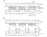
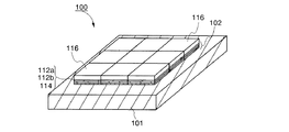
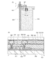
図1は、半導体基板100の構成例を示す斜視図である。半導体基板100は、1枚のベース基板101に複数の単結晶半導体層116が貼り付けられた構成を有している。各単結晶半導体層116は絶縁層102を介してベース基板101に設けられており、半導体基板100は、いわゆるSOI基板と呼ばれるものである。
FIG. 1 is a perspective view illustrating a configuration example of the
絶縁層102は、単層構造でも積層構造でもよい。本実施形態では絶縁層102は3層構造であり、ベース基板101側から、接合層114、絶縁膜112b(窒化酸化シリコン層)、絶縁膜112a(酸化窒化シリコン層)が積層されている。
The
単結晶半導体層116は、単結晶半導体基板を薄膜化することで形成される層である。該単結晶半導体基板としては、市販の半導体基板を用いることができ、例えば、単結晶シリコン基板、単結晶ゲルマニウム基板、単結晶シリコンゲルマニウム基板など、第4族元素(14族元素)でなる単結晶半導体基板を用いることができる。また、ガリウムヒ素やインジウムリン等の化合物半導体基板を用いることもできる。
The single
ベース基板101としては、絶縁表面を有する基板を用いると良い。絶縁表面を有する基板としては、電子工業用に使われる各種ガラス基板、石英基板、セラミック基板、サファイア基板等が挙げられる。コストの点からは、ベース基板101としてガラス基板を用いるのがよい。ガラス基板は、例えば、熱膨張係数が25×10−7/℃以上50×10−7/℃以下(好ましくは、30×10−7/℃以上40×10−7/℃以下)であり、歪み点が580℃以上680℃以下(好ましくは、600℃以上680℃以下)である基板を用いると良い。また、半導体装置の汚染を低減するため、ガラス基板は無アルカリガラス基板とすることが好ましい。無アルカリガラス基板は、例えば、アルミノシリケートガラス、アルミノホウケイ酸ガラス、バリウムホウケイ酸ガラスなどのガラス材料により形成されている。また、ベース基板101には、絶縁表面を有する基板の他、金属やステンレスなどの導電体でなる導電性基板、シリコンやガリウムヒ素など半導体でなる半導体基板などを用いることができる。
As the
ガラス基板としては、液晶パネルの製造用に開発されたマザーガラスを用いることが好ましい。マザーガラスとしては、例えば、第3世代(550mm×650mm)、第3.5世代(600mm×720mm)、第4世代(680mm×880mm または、730mm×920mm)、第5世代(1100mm×1300mm)第6世代(1500mm×1850mm)、第7世代(1870mm×2200mm)、第8世代(2200mm×2400mm)などのサイズの基板が知られている。大面積のマザーガラスをベース基板101として用いてSOI基板を製造することで、SOI基板の大面積化が実現できる。
As the glass substrate, it is preferable to use mother glass developed for manufacturing liquid crystal panels. As the mother glass, for example, the third generation (550 mm × 650 mm), the third generation (600 mm × 720 mm), the fourth generation (680 mm × 880 mm or 730 mm × 920 mm), the fifth generation (1100 mm × 1300 mm) Substrates of sizes such as 6th generation (1500 mm × 1850 mm), 7th generation (1870 mm × 2200 mm), 8th generation (2200 mm × 2400 mm) are known. By manufacturing an SOI substrate using a large-area mother glass as the
マザーガラスのような大面積基板をベース基板101として用いることで、SOI基板の大面積化が実現できる。SOI基板の大面積化が実現すれば、大型の半導体装置を提供することができる。また、一度に多数の集積回路(IC、LSIなどともいう)を製造することができ、1枚の基板からの取り数が増加するため、生産性を飛躍的に向上させることができる。
By using a large-area substrate such as mother glass as the
以下、図2乃至図10を参照して、図1に示す半導体基板100の作製方法を説明する。
Hereinafter, a method for manufacturing the
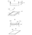
はじめに、単結晶半導体基板110を準備する。単結晶半導体基板110は、所望の大きさ、形状に加工されている。図2は、単結晶半導体基板110の構成の一例を示す外観図である。矩形のベース基板101に貼り合わせること、および縮小投影型露光装置などの露光装置の露光領域が矩形であること等を考慮すると、図2に示すように単結晶半導体基板110の形状は矩形であることが好ましい。例えば、矩形の単結晶半導体基板110の長辺が、縮小投影型露光装置の1ショットの露光領域の一辺のn倍(nは自然数)の長さとなるように加工すると、生産性の面から好ましいといえる。なお、特段の断りが無い限り、矩形には正方形が含まれることとする。
First, a single
矩形の単結晶半導体基板110は、市販の円形のバルク単結晶半導体基板を切断することで形成することができる。基板の切断には、ダイサーやワイヤソー等による切断、レーザ切断、プラズマ切断、電子ビーム切断、その他任意の切断手段を用いることができる。また、基板として薄片化する前の半導体基板製造用のインゴットを、その断面が矩形になるように直方体状に加工し、この直方体状のインゴットを薄片化することでも、矩形の単結晶半導体基板110を製造することができる。
The rectangular single
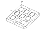
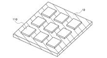
単結晶半導体基板110を洗浄した後、トレイ10に複数の単結晶半導体基板110を配置する。図3は、トレイ10の構成の一例を示す外観図である。トレイ10は、板状の部材であり、単結晶半導体基板110を保持するための複数の凹部11が形成されている。図3に示すトレイ10には、3行3列に凹部11が形成されている。もちろん、本発明は該構成に限定して解釈されるものではなく、行数及び列数を適宜変更することができる。該トレイ10を用いて、図4に示すように、トレイ10の凹部11に単結晶半導体基板110を配置する。
After the single
トレイ10は、半導体基板100の作製工程における熱処理によって、変形・変質しない材料で形成される。特に、熱膨張が少ない材料を選択することが好ましい。例えば、石英ガラスやステンレスを用いてトレイ10を作製することができる。
The
トレイ10の厚さは、例えば、1.1mm以上2mm以下とすることができる。もちろん、一定の強度が確保できる厚さであればこれに限られない。凹部11の深さは、例えば、0.2mm以上0.6mm以下とすることができ、0.3mm以上0.5mm以下とすることが好ましい。なお、凹部11の深さについては、単結晶半導体基板110を保持できる深さであればよく、前述の深さに限られるものではない。トレイ10のサイズは、ベース基板101と同程度のサイズとすることが好ましい。トレイ10とベース基板とのサイズを同程度とすることにより、貼り合わせの際の位置合わせが容易になるためである。凹部11のサイズは、単結晶半導体基板110が収まるサイズとする。好ましくは、凹部11のサイズと単結晶半導体基板110のサイズとを同程度とする。例えば、凹部11の一辺と、対応する単結晶半導体基板110の一辺との長さの差が0.5mm以下となるようにする。このように、凹部11のサイズと単結晶半導体基板110のサイズとを同程度とすることにより、貼り合わせの際の位置精度を大きく向上することができる。なお、本実施の形態の作製方法では、凹部11のサイズおよび配列によって、半導体基板100における単結晶半導体層116のサイズ、配列が決定する。
The thickness of the
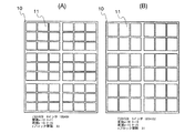
図5、図6は、トレイ10の構成例を示す上面図である。図5は、ベース基板101として、サイズが600mm×720mmであるマザーガラスを用いる場合のトレイ10の平面図であり、トレイ10のサイズは、マザーガラスと同じ600mm×720mmである。図6は、ベース基板101として、サイズが730mm×920mmである第4世代のマザーガラスを用いる場合のトレイ10の平面図であり、トレイ10のサイズは、マザーガラスと同じ730mm×920mmである。
5 and 6 are top views showing examples of the configuration of the
図5(A)は、露光領域のサイズが4インチ角の縮小投影型露光装置に対応するように、凹部11のサイズおよび配置を考慮したトレイ10の平面図である。トレイ10は4つのブロックに区分されており、各ブロックには3行3列に配置された9つの凹部11が形成されている。各凹部11のサイズは、1ショットの露光領域に収まる102mm×82mmである。一つのブロックにおいて、凹部11の間隔は、縦、横共に11mmであり、トレイ10の縁から凹部11までの距離は、縦、横共に16mmである。
FIG. 5A is a plan view of the
図5(B)は、露光領域のサイズが5インチ角の縮小投影型露光装置に対応するように、凹部11のサイズおよび配置を考慮したトレイ10の平面図である。トレイ10は4つのブロックに区分されており、各ブロックには3行2列に配置された6つの凹部11が形成されている。各凹部11のサイズは、1ショットの露光領域に収まる102mm×130mmである。一つのブロックにおいて、凹部11の間隔は、縦が11mm、横が10mmであり、トレイ10の縁から凹部11までの距離は、縦、横共に16mmである。
FIG. 5B is a plan view of the
図6(A)は、露光領域のサイズが4インチ角の縮小投影型露光装置に対応するように、凹部11のサイズおよび配置を考慮したトレイ10の平面図である。トレイ10は6つのブロックに区分されており、各ブロックには3行3列に配置された9つの凹部11が形成されている。各凹部11のサイズは、1ショットの露光領域に収まる105mm×84mmである。一つのブロックにおいて、凹部11の間隔は、縦が11mm、横が10mmであり、トレイ10の縁から凹部11までの距離は、縦が16mm、横が15mmである。
FIG. 6A is a plan view of the
図6(B)は、露光領域のサイズが5インチ角の縮小投影型露光装置に対応するように、凹部11のサイズおよび配置を考慮したトレイ10の平面図である。トレイ10は6つのブロックに区分されており、各ブロックには2行3列に配置された6つの凹部11が形成されている。各凹部11のサイズは1ショットの露光領域に収まる132mm×105mmである。一つのブロックにおいて、凹部11の間隔は、縦が13mm、横が10mmであり、トレイ10の縁から凹部11までの距離は、縦、横共に15mmである。
FIG. 6B is a plan view of the
なお、上述のトレイ10の構成はあくまで一例であり、本発明が該構成に限定して解釈されるものではない。例えば、一つのブロックにおける凹部11の間隔を狭めて、連続的に単結晶半導体基板110を配列させる構成としても良い。また、より大きいトレイを用いて、より大きいマザーガラスに対応させることもできる。
The configuration of the
図4に示すように、トレイ10に単結晶半導体基板110を配置した後、図7(A)に示すように、単結晶半導体基板110上に絶縁層112を形成する。絶縁層112は単層構造、又は、2層以上の多層構造とすることができる。また、その厚さは5nm以上400nm以下とすることができる。作製方法としては、CVD法や、スパッタ法、単結晶半導体基板110の表面を酸化又は窒化する方法などが挙げられる。絶縁層112を構成する膜としては、酸化シリコン膜、窒化シリコン膜、酸化窒化シリコン膜、窒化酸化シリコン膜、酸化ゲルマニウム膜、窒化ゲルマニウム膜、酸化窒化ゲルマニウム膜、窒化酸化ゲルマニウム膜などのシリコンまたはゲルマニウムを組成に含む絶縁膜を用いることができる。また、酸化アルミニウム膜、酸化タンタル膜、酸化ハフニウム膜などの金属の酸化物でなる絶縁膜、窒化アルミニウム膜などの金属の窒化物でなる絶縁膜、酸化窒化アルミニウム膜などの金属の酸化窒化物でなる絶縁膜、窒化酸化アルミニウム膜などの金属の窒化酸化物でなる絶縁膜を用いることもできる。
As shown in FIG. 4, after the single
ここで、酸化窒化物とは、その組成において、窒素よりも酸素の含有量が多いものを示し、例えば、酸化窒化シリコンとは、酸素が50原子%以上70原子%以下、窒素が0.5原子%以上15原子%以下、珪素が25原子%以上35原子%以下、水素が0.1原子%以上10原子%以下の範囲で含まれるものをいう。また、窒化酸化物とは、その組成において、酸素よりも窒素の含有量が多いものを示し、例えば、窒化酸化シリコンとは、酸素が5原子%以上30原子%以下、窒素が20原子%以上55原子%以下、珪素が25原子%以上35原子%以下、水素が10原子%以上30原子%以下の範囲で含まれるものをいう。但し、上記範囲は、ラザフォード後方散乱法(RBS:Rutherford Backscattering Spectrometry)や、水素前方散乱法(HFS:Hydrogen Forward Scattering)を用いて測定した場合のものである。また、構成元素の含有比率は、その合計が100原子%を超えない値をとる。 Here, the oxynitride indicates a composition whose oxygen content is higher than that of nitrogen. For example, silicon oxynitride refers to oxygen of 50 atomic% to 70 atomic% and nitrogen of 0.5%. The term includes at least 15 atomic percent and no more than 15 atomic percent, silicon at least 25 atomic percent and not more than 35 atomic percent, and hydrogen at least 0.1 atomic percent and not more than 10 atomic percent. A nitrided oxide indicates a composition whose nitrogen content is higher than that of oxygen. For example, silicon nitride oxide means that oxygen is 5 atomic% to 30 atomic% and nitrogen is 20 atomic% or more. 55 atomic% or less, silicon is 25 atomic% or more and 35 atomic% or less, and hydrogen is included in the range of 10 atomic% or more and 30 atomic% or less. However, the above ranges are those measured using Rutherford Backscattering Spectrometry (RBS) or Hydrogen Forward Scattering (HFS). Further, the content ratio of the constituent elements takes a value that the total does not exceed 100 atomic%.
ベース基板101として、アルカリ金属やアルカリ土類金属などの半導体装置の信頼性を低下させる不純物を含むような基板を用いる場合には、該不純物がベース基板101からSOI基板の半導体層に拡散することを防止できるような膜を、少なくとも1層以上、絶縁層112中に含ませることが好ましい。このような膜には、窒化シリコン膜、窒化酸化シリコン膜、窒化アルミニウム膜、または窒化酸化アルミニウム膜などがある。このような膜を含ませることで、絶縁層112をバリア層として機能させることができる。
In the case where a substrate containing an impurity such as an alkali metal or an alkaline earth metal that decreases the reliability of a semiconductor device is used as the
例えば、絶縁層112を単層構造のバリア層とする場合には、厚さ5nm以上200nm以下の窒化シリコン膜、窒化酸化シリコン膜、窒化アルミニウム膜、または窒化酸化アルミニウム膜を用いて絶縁層112を形成すればよい。
For example, in the case where the insulating
絶縁層112を、2層構造のバリア層とする場合には、上層は、バリア機能の高い絶縁膜で構成する。例えば、厚さ5nm以上200nm以下程度の窒化シリコン膜、窒化酸化シリコン膜、窒化アルミニウム膜、または窒化酸化アルミニウム膜を用いることができる。なお、これらの膜は、不純物の拡散を防止するブロッキング効果が高いが、内部応力も高い。そのため、単結晶半導体基板110と接する下層の絶縁膜としては、上層の絶縁膜の応力を緩和する効果のある膜を選択することが好ましい。このような絶縁膜には、酸化シリコン膜や酸化窒化シリコン膜、単結晶半導体基板110を熱酸化して形成した熱酸化膜などがある。下層の絶縁膜の厚さは、例えば、5nm以上300nm以下程度とすることができる。
When the insulating
本実施の形態では、絶縁層112を絶縁膜112aと絶縁膜112bでなる2層構造とする。絶縁層112をバリア層として機能させる場合の絶縁膜112aと絶縁膜112bの組み合わせとしては、例えば、酸化シリコン膜と窒化シリコン膜、酸化窒化シリコン膜と窒化シリコン膜、酸化シリコン膜と窒化酸化シリコン膜、酸化窒化シリコン膜と窒化酸化シリコン膜などがある。
In this embodiment, the insulating
例えば、下層の絶縁膜112aとしては、プロセスガスにSiH4及びN2Oを用いて、プラズマ励起CVD法(以下、PECVD法ともいう)で形成した酸化窒化シリコン膜を用いることができる。また、プロセスガスに有機シランガスと酸素を用いて、PECVD法で形成した酸化シリコン膜を用いてもよい。また、単結晶半導体基板110を酸化することにより形成した酸化膜を絶縁膜112aとすることもできる。
For example, as the lower insulating
なお、有機シランとは、珪酸エチル(TEOS:化学式Si(OC2H5)4)、テトラメチルシラン(TMS:化学式Si(CH3)4)、テトラメチルシクロテトラシロキサン(TMCTS)、オクタメチルシクロテトラシロキサン(OMCTS)、ヘキサメチルジシラザン(HMDS)、トリエトキシシラン(SiH(OC2H5)3)、トリスジメチルアミノシラン(SiH(N(CH3)2)3)などの珪素原子を含有する有機化合物をいう。 Note that the organic silane is ethyl silicate (TEOS: chemical formula Si (OC 2 H 5 ) 4 ), tetramethylsilane (TMS: chemical formula Si (CH 3 ) 4 ), tetramethylcyclotetrasiloxane (TMCTS), octamethylcyclohexane. Contains silicon atoms such as tetrasiloxane (OMCTS), hexamethyldisilazane (HMDS), triethoxysilane (SiH (OC 2 H 5 ) 3 ), trisdimethylaminosilane (SiH (N (CH 3 ) 2 ) 3 ) An organic compound.
上層の絶縁膜112bとしては、例えば、プロセスガスにSiH4、N2O、NH3及びH2を用いてPECVD法で形成した窒化酸化シリコン膜を用いることができる。プロセスガスにSiH4、N2、NH3及びH2を用いてPECVD法で形成した窒化シリコン膜を用いてもよい。
As the upper insulating
PECVD法で、酸化窒化シリコンでなる絶縁膜112a、窒化酸化シリコンでなる絶縁膜112bを形成する場合には、例えば、トレイ10に配置された複数の単結晶半導体基板110をPECVD装置の処理室に搬入し、SiH4及びN2Oの混合ガスのプラズマを生成し、酸化窒化シリコン膜を単結晶半導体基板110上に形成した後、処理室に導入するガスをSiH4、N2O、NH3及びH2に変更し、これらの混合ガスのプラズマを生成して、酸化窒化シリコン膜上に窒化酸化シリコン膜を連続して形成することができる。また、複数の処理室を有するPECVD装置を用いる場合には、酸化窒化シリコン膜と窒化酸化シリコン膜を異なる処理室で形成することもできる。もちろん、処理室に導入するガスを変更することで、下層に酸化シリコン膜を形成することもできるし、上層に窒化シリコン膜を形成することもできる。
In the case where the insulating
上記のように絶縁膜112aおよび絶縁膜112bを形成することで、スループット良く、複数の単結晶半導体基板110に絶縁層112を形成することができる。また、大気に触れさせることなく絶縁膜112a、絶縁膜112bを形成できるので、絶縁膜112aと絶縁膜112bの界面が大気によって汚染されることを防止できる。
By forming the insulating
また、絶縁膜112aとして、単結晶半導体基板110を酸化処理して形成した酸化膜を用いることができる。該酸化膜を形成するための熱酸化処理は、ドライ酸化でも良いが、酸化雰囲気中にハロゲンを含むガスを添加することが好ましい。ハロゲンを含むガスとしては、HCl、HF、NF3、HBr、Cl、ClF、BCl3、F、Br2などから選ばれた一種又は複数種のガスを用いることができる。
As the insulating
例えば、酸素に対してHClを0.5体積%以上10体積%以下(好ましくは3体積%程度)の割合で含む雰囲気中で、700℃以上の温度で熱処理を行う。一例としては、950℃以上1100℃以下の加熱温度で熱酸化を行うとよい。処理時間は0.1時間以上6時間以下、好ましくは0.5時間以上1時間以下とすることができる。形成される酸化膜の膜厚は、10nm以上1000nm以下(好ましくは50nm以上200nm以下)、例えば100nmの厚さとすることができる。 For example, heat treatment is performed at a temperature of 700 ° C. or higher in an atmosphere containing HCl at a ratio of 0.5 volume% to 10 volume% (preferably about 3 volume%) with respect to oxygen. As an example, thermal oxidation may be performed at a heating temperature of 950 ° C. or higher and 1100 ° C. or lower. The treatment time can be from 0.1 hour to 6 hours, preferably from 0.5 hour to 1 hour. The thickness of the formed oxide film can be 10 nm to 1000 nm (preferably 50 nm to 200 nm), for example, 100 nm.
このような温度範囲で酸化処理を行うことで、ハロゲン元素によるゲッタリング効果(金属不純物を除去する効果)を得ることができる。すなわち、塩素の作用により、金属などの不純物が揮発性の塩化物となって気相中へ離脱して、単結晶半導体基板110から除去される。また、酸化雰囲気に含まれるハロゲン元素により、単結晶半導体基板110の表面の欠陥が終端されるため、酸化膜と単結晶半導体基板110との界面の局在準位密度を低減できる。
By performing oxidation treatment in such a temperature range, a gettering effect (an effect of removing metal impurities) by a halogen element can be obtained. In other words, due to the action of chlorine, impurities such as metals are converted into volatile chlorides and separated into the gas phase, and are removed from the single
このハロゲンを含む雰囲気での熱酸化処理により、酸化膜にハロゲンを含ませることができる。ハロゲン元素を1×10¹⁷atoms/cm3以上5×1020atoms/cm3以下程度の濃度で含ませることにより、半導体基板100において、金属などの不純物を捕獲して単結晶半導体層116の汚染を防止する保護膜としての機能を発現させることができる。
By thermal oxidation treatment in an atmosphere containing halogen, the oxide film can contain halogen. By containing a halogen element at a concentration of about 1 × 10 17 atoms / cm 3 or more and 5 × 10 20 atoms / cm 3 or less, the
熱酸化処理で下層の絶縁膜112aを形成し、PECVD法などの気相法で上層の絶縁膜112bを形成する場合は、単結晶半導体基板110をトレイ10に配置する前に、熱酸化処理で絶縁膜112aを形成し、絶縁膜112aが形成された単結晶半導体基板110をトレイ10に並べ、しかる後に、絶縁膜112bを形成することもできる。
In the case where the lower insulating
次に、図7(B)に示すように、絶縁層112を介して、電界で加速されたイオンでなるイオンビーム121を単結晶半導体基板110に照射して、単結晶半導体基板110の表面から所定の深さの領域に、損傷領域113(脆化領域ともいう)を形成する。損傷領域113となる領域の深さは、イオンの平均侵入深さとほぼ同じ深さであり、イオンビーム121の加速エネルギーとイオンビーム121の入射角によって調節することができる。加速エネルギーは加速電圧、ドーズ量などにより調節できる。なお、損傷領域113の深さによって、単結晶半導体基板110から分離される半導体層の厚さが決定されることになる。損傷領域113が形成される深さは50nm以上500nm以下とすればよく、好ましくは50nm以上200nm以下である。
Next, as illustrated in FIG. 7B, the single
イオンを単結晶半導体基板110に照射する方法としては、質量分離を伴うイオン注入法よりも、質量分離を伴わないイオンドーピング法を用いることが好ましい。これにより、大型の(大面積な)トレイ10に配置された複数の単結晶半導体基板110に損傷領域113を形成するタクトタイムを短縮できるからである。
As a method for irradiating the single
イオンドーピング法を用いる場合には、トレイ10に収められた単結晶半導体基板110を、イオンドーピング装置の処理室に搬入する。プロセスガスを励起しプラズマを生成し、そのプラズマから所望のイオンを引き出し加速してイオンビーム121を生成し、そのイオンビーム121を、複数の単結晶半導体基板110に照射することで、所定の深さにイオンが高濃度に導入され、損傷領域113が形成される。
In the case of using the ion doping method, the single
ソースガスに水素(H2)を用いる場合、水素ガスを励起してH+、H2 +、H3 +を生成することができる。ソースガスから生成されるイオン種の割合は、プラズマの励起方法、プラズマを発生させる雰囲気の圧力、ソースガスの供給量などを調節することで、変化させることができる。イオンドーピング法を用いてイオンの照射を行う場合、イオンビーム121中のイオンの総量に対してH3 +が少なくとも50%以上含まれるようにする。H3 +が70%以上含まれるようにすることが好ましく、80%以上とするとより好ましい。H3 +の割合を50%以上とすることで、イオンビーム121に含まれるH+、H2 +の割合が相対的に小さくなるため、イオンビーム121に含まれる水素イオンの平均侵入深さのばらつきを小さくすることができる。これにより、イオンの照射効率が向上し、タクトタイムを短縮することができる。また、H3 +はH+やH2 +と比較して質量が大きいため、加速電圧が同じ場合(すなわちイオンのエネルギーが同じ場合)であれば、損傷領域を浅く形成することができる。すなわち、半導体層を薄膜化することができる。なお、H3 +の半導体基板におけるプロファイルは、H+やH2 +と比較して急峻である。つまり、照射の総量が少ない場合であっても、良好に分離を行うことができる。 When hydrogen (H 2 ) is used for the source gas, the hydrogen gas can be excited to generate H + , H 2 + , and H 3 + . The ratio of ion species generated from the source gas can be changed by adjusting the plasma excitation method, the pressure of the atmosphere in which the plasma is generated, the supply amount of the source gas, and the like. When ion irradiation is performed using an ion doping method, H 3 + is included in at least 50% or more of the total amount of ions in the ion beam 121. It is preferable that 70% or more of H 3 + is included, and more preferably 80% or more. By setting the ratio of H 3 + to 50% or more, the ratio of H + and H 2 + contained in the ion beam 121 becomes relatively small, so that the average penetration depth of hydrogen ions contained in the ion beam 121 can be reduced. Variation can be reduced. Thereby, the irradiation efficiency of ions can be improved and the tact time can be shortened. Further, since H 3 + has a larger mass than H + and H 2 + , the damaged region can be formed shallower if the acceleration voltage is the same (that is, the ion energy is the same). That is, the semiconductor layer can be thinned. Note that the profile of H 3 + in the semiconductor substrate is steep compared to H + and H 2 + . That is, even when the total amount of irradiation is small, separation can be performed satisfactorily.
ソースガスとして水素ガスを用いたイオンドーピング法によりイオン照射を行う場合、加速電圧を10kV以上200kV以下程度、ドーズ量を1×10¹⁶ions/cm2以上6×1016ions/cm2以下程度とするとよい。この条件で水素イオンを照射することにより、イオンビーム121に含まれるイオン種及びその割合にも依存するが、損傷領域113を単結晶半導体基板110の深さ50nm以上500nm以下の領域に形成することができる。
When ion irradiation is performed by an ion doping method using hydrogen gas as a source gas, an acceleration voltage is about 10 kV to 200 kV and a dose is about 1 × 10 16 ions / cm 2 to 6 × 10 16 ions / cm 2. Good. By irradiating with hydrogen ions under these conditions, the damaged
例えば、単結晶半導体基板110が単結晶シリコン基板であり、絶縁膜112aが厚さ50nmの酸化窒化シリコン膜であり、絶縁膜112bが厚さ50nmの窒化酸化シリコン膜である場合、ソースガスとして水素を用い、加速電圧が40kV、ドーズ量が2.2×10¹⁶ions/cm2の条件下では、単結晶半導体基板110から厚さ120nm程度の単結晶半導体層を分離することができる。また、絶縁膜112aを厚さ100nmの酸化窒化シリコン膜とし、他は同じ条件とした場合には、単結晶半導体基板110から厚さ70nm程度の半導体層を分離することができる。
For example, when the single
イオンビーム121のソースガスとしては、ヘリウム(He)を用いることもできる。ヘリウムを励起して生成されるイオン種はHe+が殆どであるため、質量分離を伴わないイオンドーピング法でも、He+を主たるイオンとして単結晶半導体基板110に照射することができる。よって、イオンドーピング法で、効率良く損傷領域113を形成することができる。ヘリウムを用いたイオンドーピング法を用いてイオン照射を行う場合には、加速電圧10kV以上200kV以下、ドーズ量1×10¹⁶ions/cm2以上6×1016ions/cm2以下とすればよい。なお、その他に、ソースガスとして、塩素ガス(Cl2ガス)やフッ素ガス(F2ガス)などのハロゲンガスを用いることができる。
As a source gas of the ion beam 121, helium (He) can also be used. Since most of the ion species generated by exciting helium are He + , the single
損傷領域113を形成した後、図7(C)に示すように、絶縁層112の上面に接合層114を形成する。接合層114を形成する工程では、単結晶半導体基板110の加熱温度は損傷領域113に照射した元素または分子が析出しない温度とし、その加熱温度は400℃以下、より好ましくは350℃以下である。言い換えると、この加熱温度は損傷領域113からガスが抜けない温度である。なお、接合層114は、イオン照射工程を行う前に形成することもできる。この場合には、接合層114を形成する際のプロセス温度は、350℃以上とすることができる。
After the damaged
接合層114は、平滑な親水性表面を有する層である。接合層114の算術平均粗さRaは0.7nm以下、より好ましくは、0.4nm以下である。また、接合層114の厚さは5nm以上500nm以下とすることができ、より好ましくは10nm以上200nm以下である。
The
接合層114としては、化学的気相反応により形成される絶縁膜を用いることが好ましく、中でも酸化シリコン膜が好ましい。接合層114として、プラズマ励起CVD法で酸化シリコン膜を形成する場合には、ソースガスとして有機シランガス及び酸素(O2)ガスを用いることが好ましい。ソースガスとして有機シランを用いることにより、プロセス温度が400℃以下で、平滑な表面を有する酸化シリコン膜を形成することができる。
As the
例えば、ソースガスにTEOSとO2を用いて、酸化シリコン膜でなる接合層114を形成するためには、TEOSの流量が15sccm、O2の流量が750sccm、成膜圧力は100Pa、成膜温度は300℃、電源周波数は13.56MHz、RF出力は300Wとすればよい。
For example, in order to form the
プラズマ励起CVD法以外にも、熱CVD法を用いることで接合層114として機能する酸化シリコン膜を形成することができる。この場合、シリコンのソースガスとしてはモノシラン(SiH4)やジシラン(Si2H6)などを、酸素のソースガスとしては酸素(O2)ガスや一酸化二窒素(N2O)ガスなどを用いることができる。加熱温度は200℃以上500℃以下とすることが好ましい。なお、接合層114は絶縁性材料を用いて形成されることが多く、接合層114は広く絶縁層に含まれている。なお、上述のような方法により形成された接合層114は低温での接合に有利であると考えられる。これは、上述の接合層114では、その表面にOH基が存在しているためである。接合に係るメカニズムが完全に解明されているわけではないが、Si−OHとSi−OHとが反応することによりSi−O−Siが形成されているか、又は、Si−HとSi−OHとが反応することによりSi−O−Siが形成されているものと考えられる。一方で、熱酸化法などにより形成された接合層114は表面のOH基が少なく、この意味においても低温での接合には向かないといえる。
In addition to the plasma enhanced CVD method, a silicon oxide film functioning as the
次に、絶縁層112および接合層114が形成された単結晶半導体基板110をトレイ10からはずし、複数の単結晶半導体基板110を洗浄する。この洗浄工程は、純水による超音波洗浄で行うことができる。超音波洗浄はメガヘルツ超音波洗浄(メガソニック洗浄)とすることが好ましい。超音波洗浄の後、単結晶半導体基板110をオゾン水で洗浄してもよい。オゾン水で洗浄することで、有機物の除去と、接合層114表面の親水性を向上させる表面活性化処理を行うことができる。洗浄処理、および表面活性化処理の終了後、図7(D)に示すように単結晶半導体基板110をトレイ10の凹部11に配置する。なお、本実施の形態においては、単結晶半導体基板110をトレイ10からはずして洗浄処理や活性化処理を施す場合について説明したが、本発明はこれに限定して解釈されない。単結晶半導体基板110の汚染等が問題とならない場合には、単結晶半導体基板110の洗浄を行う必要はない。また、洗浄処理や表面活性化処理を行う場合であっても、単結晶半導体基板110をトレイ10からはずさずに処理することができる。
Next, the single
接合層114の表面の活性化処理としては、オゾン水による洗浄の他、原子ビームやイオンビームの照射処理、プラズマ処理、ラジカル処理等を挙げることができる。原子ビーム若しくはイオンビームを利用する場合には、アルゴン等の不活性ガス中性原子ビームや不活性ガスイオンビームを用いることができる。
Examples of the activation treatment of the surface of the
次に、トレイ10に配置された単結晶半導体基板110とベース基板101を貼り合わせる。貼り合わせる前に、ベース基板101の洗浄をしておくことが好ましい。ベース基板101の洗浄としては、塩酸と過酸化水素水を用いた洗浄や、メガヘルツ超音波洗浄などが挙げられる。また、ベース基板101の接合面となる表面に対して、接合層114と同様に表面活性化処理を行うことが好ましい。
Next, the single
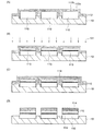
図8(A)は接合工程を説明する断面図である。複数の単結晶半導体基板110が配置されたトレイ10に対してベース基板101を配置する。そして、ベース基板101の所定の部分(例えば、端部など)に300N/cm2以上15000N/cm2以下程度の圧力を加える。この圧力は、1000N/cm2以上5000N/cm2以下程度とすることが好ましい。圧力を加えることにより、圧力を加えた部分から、接合層114とベース基板101とが密着し始める。やがて、1枚のベース基板101に対して、トレイ10上の全ての単結晶半導体基板110が密着することになる。該接合工程は、加熱処理を伴わず、常温で行うことができるため、ベース基板101としてガラス基板などの耐熱性の低い基板を用いることが可能である。
FIG. 8A is a cross-sectional view illustrating a bonding process. A
なお、本発明においては、複数の単結晶半導体基板110をトレイ10に並べているため、単結晶半導体基板110の厚さの違いにより、ベース基板101と接触しない単結晶半導体基板110が生じる場合がある。このため、圧力をかける場所は一箇所ではなく、複数箇所とすることが好ましい。より好ましくは、各単結晶半導体基板110に圧力をかけるようにする。なお、単結晶半導体基板110がトレイ10に配置された状態において、接合層114表面の高さが多少違っていたとしても、ベース基板101のたわみにより接合層114の一部分がベース基板101と接触すれば、接合層114の表面全体に接合を進行させることが可能である。
Note that in the present invention, since the plurality of single
また、図8(A)のようにベース基板101をトレイ10に載せた後、図9のようにベース基板101を下側とすることで、単結晶半導体基板110の自重によりベース基板101と単結晶半導体基板110を接触させることができる。これにより、単結晶半導体基板110の厚さの違いに関わらず、容易に接合を形成することができる。
Further, after the
ベース基板101に単結晶半導体基板110を貼り合わせた後には、ベース基板101と接合層114との界面における結合力を増加させるために、加熱処理を施すことが好ましい。この処理温度は、損傷領域113に亀裂を発生させない温度とし、例えば、200℃以上450℃以下の温度範囲とすることができる。また、この温度範囲で加熱しながら、ベース基板101に単結晶半導体基板110を貼り合わせることで、ベース基板101と接合層114との接合界面での結合力を強固なものとすることができる。
After the single
単結晶半導体基板110上にベース基板101を配置する際に接合面がゴミなどにより汚染されてしまうと、該汚染された部分は接合されなくなる。このような接合面の汚染を防ぐため、ベース基板101の単結晶半導体基板110上への配置は、気密構造の処理室(気密室)内において行うことが好ましい。また、該処理室内を5.0×10⁻³Pa程度の減圧状態とし、接合処理が行われる雰囲気を清浄にしておくことが好ましい。
If the bonding surface is contaminated with dust or the like when the
次いで、加熱処理を行い、損傷領域113で分離させて、単結晶半導体基板110から半導体層115を分離する。図8(B)は、単結晶半導体基板110から半導体層115を分離する分離工程を説明する図である。なお、ここでは、半導体層115が分離された後の単結晶半導体基板を単結晶半導体基板117としている。
Next, heat treatment is performed so that the
加熱処理により、損傷領域113に存在する元素が析出し、損傷領域113の微小な空洞内の圧力が上昇する。この圧力の上昇により、損傷領域113の微小な空洞の体積変化が生じ、損傷領域113に亀裂が生じる。これにより、損傷領域113に沿って単結晶半導体基板110が分離される。接合層114はベース基板101と接合しているので、ベース基板101上には単結晶半導体基板110から分離された半導体層115が固定される。半導体層115を単結晶半導体基板110から分離するための加熱処理の温度は、ベース基板101の歪み点を越えない温度とする。
By the heat treatment, elements present in the damaged
この加熱処理には、RTA(Rapid Thermal Anneal)装置、抵抗加熱炉、マイクロ波加熱装置などを用いることができる。RTA装置としては、GRTA(Gas Rapid Thermal Anneal)装置や、LRTA(Lamp Rapid Thermal Anneal)装置が挙げられる。 For this heat treatment, an RTA (Rapid Thermal Anneal) apparatus, a resistance heating furnace, a microwave heating apparatus, or the like can be used. Examples of the RTA apparatus include a GRTA (Gas Rapid Thermal Anneal) apparatus and an LRTA (Lamp Rapid Thermal Anneal) apparatus.
GRTA装置を用いる場合には、加熱温度550℃以上650℃以下、処理時間0.5分以上60分以内の加熱処理を適用することができる。抵抗加熱装置を用いる場合には、加熱温度200℃以上650℃以下、処理時間2時間以上4時間以内の加熱処理を適用することができる。マイクロ波処理装置を用いる場合には、マイクロ波周波数を2.45GHzとし、処理時間10分以上20分以内の加熱処理を適用することができる。 In the case of using a GRTA apparatus, heat treatment with a heating temperature of 550 ° C. or higher and 650 ° C. or lower and a treatment time of 0.5 minutes or longer and within 60 minutes can be applied. In the case of using a resistance heating device, a heat treatment with a heating temperature of 200 ° C. or higher and 650 ° C. or lower and a treatment time of 2 hours or longer and within 4 hours can be applied. In the case of using a microwave treatment apparatus, a heat treatment with a microwave frequency of 2.45 GHz and a treatment time of 10 minutes to 20 minutes can be applied.
抵抗加熱装置を有する縦型炉を用いた加熱処理の具体的な処理方法を説明する。はじめに、図8(A)の、トレイ10に配置された単結晶半導体基板110が貼り付けられたベース基板101を、縦型炉のボートに配置する。そして該ボートを縦型炉のチャンバーに搬入する。チャンバー内は、単結晶半導体基板110の酸化を抑制するために真空状態(減圧状態)とする。真空度は、5×10⁻³Pa程度とすればよい。真空状態にした後、窒素をチャンバー内に供給して、チャンバー内を大気圧の窒素雰囲気にする。この間に、温度を200℃に上昇させる。
A specific treatment method of heat treatment using a vertical furnace having a resistance heating device will be described. First, the
温度200℃で2時間加熱した後、1時間かけて400℃に上昇させる。温度400℃の状態が安定したら、さらに1時間かけて600℃に上昇させる。温度600℃の状態が安定したら、600℃で2時間加熱処理する。その後、1時間かけて、温度400℃まで下げ、その10分乃至30分間後に、チャンバー内からボートを搬出する。そして、大気雰囲気下で、ボート上のトレイ10に並べられた単結晶半導体基板117、および半導体層115が貼り付けられたベース基板101を冷却する。
After heating at 200 ° C. for 2 hours, the temperature is raised to 400 ° C. over 1 hour. When the temperature of 400 ° C is stabilized, the temperature is further increased to 600 ° C over 1 hour. When the temperature of 600 ° C. is stabilized, heat treatment is performed at 600 ° C. for 2 hours. Thereafter, the temperature is lowered to 400 ° C. over 1 hour, and after 10 to 30 minutes, the boat is unloaded from the chamber. Then, the single
上記の抵抗加熱炉を用いた加熱処理では、接合層114とベース基板101との結合力を強化するための加熱処理と、損傷領域113での分離を生じさせる加熱処理が連続して行われる。この2つの加熱処理を異なる装置で行う場合には、例えば、次のような工程を用いることができる。まず、抵抗加熱炉を用いて、200℃、2時間の加熱処理を行う。そして、貼り合わされたベース基板101と単結晶半導体基板110を炉から搬出し、その後、RTA装置で、600℃以上700℃以下、1分以上30分以下の加熱処理を行う。該工程により、単結晶半導体基板110を損傷領域113で分割させることができる。
In the heat treatment using the resistance heating furnace, the heat treatment for strengthening the bonding force between the
なお、図8(B)に示すように、単結晶半導体基板110の周辺部がベース基板101に接合しない場合が多くある。これは、単結晶半導体基板110の周辺部が面取りされており曲率を有しているためベース基板101と接合層104が密着しない、単結晶半導体基板110の周辺部では損傷領域113が分離しにくい、周辺部の平坦性が不足している、周辺部に傷や汚れがある、などの理由によるものと考えられる。このため、ベース基板101には、単結晶半導体基板110よりもサイズが小さい半導体層115が貼り付けられ、また、単結晶半導体基板117の周囲には凸部が形成され、その凸部上に、ベース基板101に貼り付けられなかった、絶縁膜112a、絶縁膜112b、及び接合層114が残存している。
Note that as illustrated in FIG. 8B, the periphery of the single
ベース基板101に密着された半導体層115には、損傷領域113の形成の際のイオン照射や、損傷領域113における分離によって、結晶欠陥が形成されている。また、その表面の平坦性が損なわれている。このような結晶欠陥を低減し、平坦性を向上するために、図10(A)に示す様に、半導体層115にレーザビーム122を照射する。
Crystal defects are formed in the
レーザビーム122を半導体層115の上面側から照射することで、半導体層115を上面から溶融させる。溶融させた後、半導体層115が冷却、固化することにより、図10(B)に示すような、上面の平坦性が向上された単結晶半導体層116が形成される。なお、図10(B)の斜視図が図1に対応している。
The
本実施の形態においては、平坦性を向上するためにレーザビーム122の照射を行っている。このため、加熱処理による平坦化の場合と比較してベース基板101の温度上昇を抑えることができる。つまり、ガラス基板のような耐熱性の低い基板をベース基板101として用いることが可能になる。なお、レーザビーム122の照射による半導体層115の溶融は、部分溶融であることが好ましい。完全溶融させた場合には、液相となった半導体層115における無秩序な核発生により、半導体層115が再結晶化することとなり、半導体層115の結晶性が低下するためである。部分溶融させることにより、溶融されていない固相部分から結晶成長が進行する。これにより、半導体層115の欠陥が減少し、結晶性が回復する。なお、完全溶融とは、半導体層115が接合層114との界面まで溶融され、液体状態になることをいう。他方、部分溶融とは、上層は溶融して液相となるが、下層は溶融せずに固相のままであることをいう。
In this embodiment mode, irradiation with the
レーザビーム122を発振するレーザ発振器としては、その発振波長が、紫外光域から可視光域にあるものが選択される。レーザビーム122の波長は、半導体層115に吸収される波長とする必要がある。その波長は、レーザビームの表皮深さ(skin depth)などを考慮して決定すればよい。例えば、250nm以上700nm以下の範囲とすることができる。
As the laser oscillator that oscillates the
上述のレーザ発振器としては、連続発振レーザ、疑似連続発振レーザ及びパルス発振レーザを用いることができる。部分溶融させるためには、パルス発振レーザを用いることが好ましい。例えば、パルス発振レーザの場合は、繰り返し周波数1MHz以下、パルス幅10n秒以上500n秒以下である。例えば、繰り返し周波数10Hz乃至300Hz、パルス幅25n秒、波長308nmのXeClエキシマレーザを用いることができる。 As the above-described laser oscillator, a continuous wave laser, a pseudo continuous wave laser, or a pulsed laser can be used. In order to perform partial melting, it is preferable to use a pulsed laser. For example, in the case of a pulsed laser, the repetition frequency is 1 MHz or less and the pulse width is 10 nsec or more and 500 nsec or less. For example, an XeCl excimer laser having a repetition frequency of 10 Hz to 300 Hz, a pulse width of 25 ns, and a wavelength of 308 nm can be used.
また、レーザビーム122のエネルギーは、レーザビーム122の波長、表皮深さ、半導体層115の膜厚などを考慮して決定することができる。レーザビーム122の照射エネルギー密度は、300mJ/cm2以上800mJ/cm2以下程度の範囲とすることができる。例えば、半導体層115の厚さが120nm程度であり、レーザ発振器にパルス発振レーザを用い、レーザビーム122の波長が308nmの場合には、レーザビーム122の照射エネルギー密度は600mJ/cm2以上700mJ/cm2以下程度とすることができる。
The energy of the
レーザビーム122を照射する際の雰囲気は、希ガス雰囲気や窒素雰囲気のような不活性雰囲気、又は、真空状態(減圧状態)で行うことが好ましい。不活性雰囲気中でレーザビーム122を照射するには、気密構造のチャンバー内の雰囲気を制御し、該チャンバー内においてレーザビーム122を照射すればよい。チャンバーを用いない場合には、例えば、レーザビーム122の被照射面に窒素ガスなどの不活性ガスを吹き付けることにより、不活性雰囲気でのレーザビーム122の照射を実現できる。不活性雰囲気や真空状態のほうが、大気雰囲気よりも平坦性を向上させる効果が高い。また、これらの雰囲気のほうが大気雰囲気よりもクラックやリッジの発生を抑制できるため好ましい。
The atmosphere for irradiation with the
レーザビーム122としては、光学系を用いてエネルギー分布を均一にし、かつ断面の形状を線状にしたものを用いることが好ましい。これにより、スループット良くレーザビーム122を照射することができ、また、レーザビーム122の照射を均一に行うことができる。レーザビーム122のビーム長をベース基板101の一辺より長くすることにより、一回の走査で、ベース基板101に貼り付けられた全ての半導体層115にレーザビーム122を照射することができる。レーザビーム122のビーム長がベース基板101の一辺より短い場合には、複数回の走査で、ベース基板101に貼り付けられた全ての半導体層115にレーザビーム122を照射することができるビーム長を選択すればよい。
As the
なお、レーザビーム122を半導体層115に照射する前に、半導体層115の表面に形成されている自然酸化膜などの酸化膜を除去する処理を行う。酸化膜を除去するのは、半導体層115表面に酸化膜が残存した状態でレーザビーム122を照射しても、平坦化の効果を十分に得ることができないためである。酸化膜の除去処理は、フッ酸を用いて行うことができる。フッ酸による処理は、半導体層115の表面が撥水性を示すまで行うことが望ましい。撥水性を示す状態とすることで、半導体層115から酸化膜が除去されたことが確認できるためである。
Note that before the
図10(A)のレーザビーム122の照射工程は、次のように行うことができる。まず、半導体層115を1/100の濃度となるように(100倍に)希釈されたフッ酸で110秒間処理して、表面の酸化膜を除去する。レーザビーム122の発振器としては、XeClエキシマレーザ(波長:308nm、パルス幅:25n秒、繰り返し周波数60Hz)を用いる。光学系により、レーザビーム122の断面を300mm×0.34mmの線状に整形する。レーザビーム122の走査速度は2.0mm/秒とし、スキャンピッチを33μm、ビームショット数を約10ショットとして、レーザビーム122を半導体層115に照射する。照射面には窒素ガスを吹き付けながら、レーザビーム122を走査する。ベース基板101が730mm×920mmの場合には、レーザビーム122を3回走査することで、ベース基板101に貼り付けられた全ての半導体層115にレーザビーム122を照射することができる。
The irradiation step with the
レーザビーム122を照射した後、単結晶半導体層116に対して500℃以上650℃以下の加熱処理を行うことが好ましい。この加熱処理によって、レーザビーム122の照射で回復されなかった単結晶半導体層116の欠陥を消滅させ、また、単結晶半導体層116の歪みを緩和することができる。この加熱処理には、RTA(Rapid Thermal Anneal)装置、抵抗加熱炉、マイクロ波加熱装置などを用いることができる。例えば、抵抗加熱炉を用いた場合には、500℃の温度で1時間加熱した後、550℃で4時間加熱するとよい。
After irradiation with the
以上の工程により、図1及び図10(B)に示す半導体基板100を作製することができる。本実施の形態により、トレイ10に配置された複数の単結晶半導体基板110に対して、絶縁層112の形成、損傷領域113の形成及び接合層114の形成を、一括して行うことができる。これにより、スループットよく半導体基板100を形成することができる。また、トレイ10に単結晶半導体基板110を配置した状態で、ベース基板101と貼り合わせているため、複数の単結晶半導体基板110をスループット良く、かつ容易にベース基板101に貼り合わせることができる。
Through the above steps, the
なお、図7(A)から図7(C)までの工程では、単結晶半導体基板110を別のトレイ10に移し替えることはしなかったが、工程毎に、その工程で使用する装置専用のトレイ10に単結晶半導体基板110を移しかえてもよい。例えば、図7(A)の絶縁層112の形成工程では、PECVD装置専用のトレイ10を使用し、図7(C)の工程ではドーピング装置専用のトレイ10を使用する、といったこともできる。
7A to 7C, the single
また、図7(A)の絶縁層112の形成工程の後、絶縁層112が形成された単結晶半導体基板110をトレイ10から取り出し、この単結晶半導体基板110に対して超音波洗浄などの洗浄処理を行い、清浄な別のトレイ10に単結晶半導体基板110を配置する、といったこともできる。
Further, after the step of forming the insulating
また、図7(B)の損傷領域113の形成工程の後、損傷領域113が形成された単結晶半導体基板110をトレイ10から取り出し、この単結晶半導体基板110に対して超音波洗浄などの洗浄処理を行い、清浄な別のトレイ10に単結晶半導体基板110を配置する、といったこともできる。
7B, after the step of forming the damaged
(実施の形態2)
本実施の形態では、単結晶半導体基板の再生処理について説明する。具体的には、図11を用いて、図8(B)に示す単結晶半導体基板117を再生処理する場合について説明する。
(Embodiment 2)
In this embodiment, a process for recycling a single crystal semiconductor substrate is described. Specifically, the case where the single
図8(B)の工程の後には、図11に示すように、単結晶半導体基板117の周囲に凸部117aが形成され、その凸部117a上に、絶縁膜112a、絶縁膜112b及び接合層114が残存している。
After the step of FIG. 8B, as shown in FIG. 11, a
まず、絶縁膜112b、絶縁膜112aおよび接合層114を除去するエッチング処理を行う。これらの膜が、酸化シリコン、酸化窒化シリコン、窒化酸化シリコンで形成されている場合には、例えば、フッ酸を用いたウエットエッチング処理を行えばよい。該エッチング処理により、図11(B)に示すような単結晶半導体基板117が得られる。図11(C)は、図11(B)の一点鎖線XYにおける断面図である。
First, an etching process for removing the insulating
次に、図11(B)及び図11(C)に示す単結晶半導体基板117をエッチング処理して、凸部117a及び分離面117bを除去する。図11(C)の破線で囲った部分は、このエッチング処理によって、除去すべき部分である。このエッチングにより、単結晶半導体基板117に残存する損傷領域113を除去する。単結晶半導体基板117のエッチング処理はウエットエッチング処理が好ましく、エッチング液としては、水酸化テトラメチルアンモニウム(tetramethylammonium hydroxide、略称;TMAH)溶液を用いることができる。
Next, the single
単結晶半導体基板117をエッチング処理して、凸部117a、分離面117b、及び損傷領域113を除去した後、その表面を機械的に研磨し、図11(D)に示すような平滑な表面を有する単結晶半導体基板118を形成する。この単結晶半導体基板118は、図2に示す単結晶半導体基板110として再利用することができる。
The single
研磨処理としては、化学機械研磨(Chemical Mechanical Polishing、略称:CMP)を用いることができる。単結晶半導体基板118の表面を平滑にするため、1μm以上10μm以下程度研磨することが望ましい。研磨後は、単結晶半導体基板118表面に研磨粒子などが残るため、フッ酸洗浄やRCA洗浄を行う。
As the polishing treatment, chemical mechanical polishing (abbreviation: CMP) can be used. In order to smooth the surface of the single
本実施の形態に示したように単結晶半導体基板を再利用することで、半導体基板100の材料コストを削減することができる。
By reusing a single crystal semiconductor substrate as shown in this embodiment mode, the material cost of the
本実施の形態は実施の形態1と組み合わせて用いることができる。 This embodiment can be used in combination with Embodiment 1.
(実施の形態3)
本実施の形態では、複数の単結晶半導体層を基板上に有する半導体基板の別の例として、ベース基板上にバリア層として機能する絶縁層を有する場合について図12を参照して説明する。なお、本実施の形態の半導体基板の作製方法の大部分については、実施の形態1を参照することができる。
(Embodiment 3)
In this embodiment, as another example of a semiconductor substrate having a plurality of single crystal semiconductor layers over a substrate, the case where an insulating layer functioning as a barrier layer is provided over a base substrate will be described with reference to FIGS. Note that Embodiment 1 can be referred to for most of the methods for manufacturing the semiconductor substrate of this embodiment.
図12(A)は、半導体基板100の構成例を示す斜視図である。図12(B)はその断面図である。半導体基板100は、1枚のベース基板101に複数の単結晶半導体層116が貼り付けられた構成を有している。各単結晶半導体層116は絶縁層102及び絶縁層103を介してベース基板101に設けられており、半導体基板100は、いわゆるSOI基板と呼ばれるものである。
FIG. 12A is a perspective view illustrating a configuration example of the
ここで、実施の形態1において示した構成と特に異なる部分は、ベース基板101上の全面に絶縁層103が形成されている点である。絶縁層103はバリア層としての機能を有している。このようにベース基板101上の全面にバリア層として機能する絶縁層103を設けることにより、単結晶半導体層116の下部にのみ絶縁層を設ける構成と比較して、より有効なバリア層を構築することができる。すなわち、単結晶半導体層116の下部のみに絶縁層を設けた場合(図12(C)参照)には、単結晶半導体層116が設けられていない領域に、不純物元素の侵入経路(例えば、ルートAのような経路)が存在するが、ベース基板101上を完全にカバーするように絶縁層を設けることによって、僅かな侵入経路をも排除することができる。これにより、バリア機能をより一層強化することができる。
Here, a part different from the structure shown in Embodiment Mode 1 is that an insulating
なお、バリア層として機能する絶縁層の具体例については、実施の形態1を参照することができるため、ここでは省略する。本実施の形態においては、絶縁層103を窒化酸化珪素膜(下層)と酸化窒化珪素膜(上層)の積層構造としたが、これに限定して解釈されるものではない。例えば、上層を酸化珪素膜とし、下層を窒化珪素膜としても良い。また、絶縁層103は単層構造としても良いし、3層以上の多層構造としても良い。絶縁層103を単層構造で形成する場合には、例えば、窒化シリコンを用いることができる。なお、本実施の形態においては、絶縁層102を接合層114のみで形成した例を示しているが、実施の形態1における絶縁層112のような、バリア層として機能する絶縁層などを設ける構成としても良い。この場合には、バリア機能をより一層向上させることができる。また、半導体層の界面を良好に保つために、絶縁層112の半導体層と接触する領域に、酸化珪素膜や酸化窒化珪素膜などを設けても良い。
Note that for a specific example of the insulating layer functioning as a barrier layer, Embodiment Mode 1 can be referred to; therefore, description thereof is omitted here. Although the insulating
本実施の形態に係る半導体基板100の構成は、絶縁層102及び絶縁層103のみにおいて実施の形態1と異なっている。このため、絶縁層102及び絶縁層103以外の構成については実施の形態1を参照すればよい。作製方法についても同様に、実施の形態1を参照することができる。
The configuration of the
本実施の形態は実施の形態1及び2と適宜組み合わせて用いることができる。 This embodiment mode can be combined with Embodiment Modes 1 and 2 as appropriate.
(実施の形態4)
本実施の形態では、複数の単結晶半導体層を基板上に有する半導体基板の別の例として、複数の単結晶半導体層を隙間なく敷き詰めた構造の半導体基板について、図13乃至図16を参照して説明する。なお、本実施の形態の半導体基板の作製方法の多くの部分については、実施の形態1を参照することができる。
(Embodiment 4)
In this embodiment, as another example of a semiconductor substrate having a plurality of single crystal semiconductor layers over the substrate, a semiconductor substrate having a structure in which the plurality of single crystal semiconductor layers are spread without gaps is described with reference to FIGS. I will explain. Note that Embodiment 1 can be referred to for many portions of the method for manufacturing a semiconductor substrate of this embodiment.
図13は、半導体基板100の構成例を示す斜視図である。半導体基板100は、1枚のベース基板101に複数の単結晶半導体層116が貼り付けられた構成を有している。各単結晶半導体層116は絶縁層102を介してベース基板101に設けられており、半導体基板100は、いわゆるSOI基板と呼ばれるものである。
FIG. 13 is a perspective view illustrating a configuration example of the
ここで、実施の形態1において示した構成と特に異なる部分は、単結晶半導体層116がベース基板101上に隙間なく敷き詰められている点である。このように、単結晶半導体層116を隙間なく敷き詰めることにより、表示装置等の大面積が必要とされる半導体装置を作製することができるようになる。具体的には、隣接する単結晶半導体層116同士の間隔を0.5mm以下、好ましくは0.3mm以下とすることにより、実質的な隙間をなくした構成とすることができる。
Here, a part that is particularly different from the structure described in Embodiment 1 is that the single
なお、本実施の形態に示す半導体基板を作製するためには、用いる単結晶半導体基板の平坦性や、カッティングの精度、その他単結晶半導体基板の特性が非常に重要である。実施の形態1において説明したように、単結晶半導体基板の周辺部が曲率を有している場合や、周辺部の平坦性が不足している場合、周辺部に傷や汚れがある場合などには、周辺部の接合が不十分になる。したがって、これらの点に留意する必要がある。 Note that in order to manufacture the semiconductor substrate described in this embodiment, flatness of a single crystal semiconductor substrate to be used, cutting accuracy, and other characteristics of the single crystal semiconductor substrate are very important. As described in Embodiment Mode 1, when the peripheral portion of the single crystal semiconductor substrate has a curvature, when the flatness of the peripheral portion is insufficient, or when the peripheral portion has scratches or dirt, etc. In such a case, bonding at the peripheral portion becomes insufficient. Therefore, it is necessary to pay attention to these points.
図14に、本実施の形態において用いるトレイ10の構成の一例を示す。トレイ10は、板状の部材であり、単結晶半導体基板110を保持するための凹部11が形成されている。このように、凹部11を、複数の単結晶半導体基板110を隙間なく並べることができる形状とすることで、単結晶半導体層116を隙間なく敷き詰めた構造の半導体基板100を作製することができる。なお、ここでは、3行3列に単結晶半導体基板110を配列させて一つのブロックとする場合の凹部11を示しているが、本発明は該構成に限定して解釈されるものではなない。例えば、行数及び列数を適宜変更しても良い。該トレイ10を用いて、図15に示すように、トレイ10の凹部11に複数の単結晶半導体基板110を配置し、各工程を経ることにより図13に示す半導体基板100が完成する。なお、図16は、図13の断面図に対応している。トレイ10の材質、大きさなどについては実施の形態1を参照することができるため、ここでは省略する。
FIG. 14 shows an example of the configuration of the
本実施の形態に係る半導体基板100の構成は、複数の単結晶半導体層を隙間なく敷き詰めた点のみにおいて実施の形態1と異なっている。このため、該構成以外については実施の形態1を参照すればよい。
The configuration of the
本実施の形態は実施の形態1乃至3と適宜組み合わせて用いることができる。 This embodiment can be combined with any of Embodiments 1 to 3 as appropriate.
(実施の形態5)
本実施の形態では、半導体基板100を用いた半導体装置の作製方法の一例として、薄膜トランジスタを作製する方法を説明する。複数の薄膜トランジスタを組み合わせることで、各種の半導体装置が形成される。本実施の形態では、実施の形態1の作製方法で作製した半導体基板100を用いることにする。
(Embodiment 5)
In this embodiment, a method for manufacturing a thin film transistor is described as an example of a method for manufacturing a semiconductor device using the
まず、図17(A)に示すように、ベース基板101上の単結晶半導体層116をエッチングにより所望の形状に加工(パターニング)することで、半導体膜603と半導体膜604とを形成する。
First, as illustrated in FIG. 17A, the single
半導体膜603と半導体膜604には、閾値電圧を制御するために、硼素、アルミニウム、ガリウムなどのp型不純物や、リン、砒素などのn型不純物が添加されていても良い。例えば、p型を付与する不純物としてボロンを添加する場合、5×1016cm−3以上1×1017cm−3以下の濃度で添加すれば良い。閾値電圧を制御するための不純物の添加は、単結晶半導体層116に対して行っても良いし、半導体膜603と半導体膜604に対して行っても良い。また、閾値電圧を制御するための不純物の添加を、単結晶半導体基板110に対して行っても良い。若しくは、不純物の添加を、閾値電圧を大まかに調整するために単結晶半導体基板110に対して行った上で、閾値電圧を微調整するために、単結晶半導体層116に対して、または半導体膜603及び半導体膜604に対して行うようにしても良い。
The
また半導体膜603と半導体膜604を形成した後、ゲート絶縁膜606を形成する前に水素化処理を行っても良い。水素化処理は、例えば、水素雰囲気中において350℃、2時間程度行う。
Alternatively, hydrogen treatment may be performed after the
次に、図17(B)に示すように、半導体膜603と半導体膜604を覆うように、ゲート絶縁膜606を形成する。ゲート絶縁膜606は、高密度プラズマ処理を行うことにより半導体膜603と半導体膜604の表面を酸化または窒化することで形成することができる。高密度プラズマ処理は、例えばHe、Ar、Kr、Xeなどの希ガスと、酸素、酸化窒素、アンモニア、窒素、水素などのガスの混合ガスを用いて行う。この場合、プラズマの励起をマイクロ波の導入により行うことで、低電子温度で高密度のプラズマを生成することができる。このような高密度のプラズマで生成された酸素ラジカル(OHラジカルを含む場合もある)や窒素ラジカル(NHラジカルを含む場合もある)によって、半導体膜の表面を酸化または窒化することにより、1nm以上20nm以下、望ましくは5nm以上10nm以下の絶縁膜を半導体膜に接するように形成する。該絶縁膜をゲート絶縁膜606として用いる。
Next, as illustrated in FIG. 17B, a
上述した高密度プラズマ処理による半導体膜の酸化または窒化は固相反応で進むため、ゲート絶縁膜606と半導体膜603及び半導体膜604との界面準位密度をきわめて低くすることができる。また、高密度プラズマ処理により半導体膜を直接酸化又は窒化することで、形成される絶縁膜の厚さのばらつきを抑えることが出来る。また、半導体膜が結晶性を有するため、高密度プラズマ処理を用いて半導体膜の表面を固相反応で酸化させる場合であっても、結晶粒界における不均一な酸化を抑え、均一性が良く、界面準位密度の低いゲート絶縁膜を形成することができる。このように、高密度プラズマ処理により形成された絶縁膜を、ゲート絶縁膜の一部または全部に含んで形成されるトランジスタは、特性のばらつきを抑えることができる。
Since the oxidation or nitridation of the semiconductor film by the high-density plasma treatment described above proceeds by a solid phase reaction, the interface state density between the
或いは、半導体膜603と半導体膜604を熱酸化させることで、ゲート絶縁膜606を形成するようにしても良い。このような熱酸化を用いる場合には、耐熱性の比較的高いベース基板を用いることが好ましい。
Alternatively, the
また、プラズマCVD法又はスパッタリング法などを用い、酸化珪素、窒化酸化珪素、窒化珪素、酸化ハフニウム、酸化アルミニウムまたは酸化タンタルを含む膜を、単層で形成することにより、又は、積層させることで、ゲート絶縁膜606を形成しても良い。
In addition, by using a plasma CVD method or a sputtering method, a film containing silicon oxide, silicon nitride oxide, silicon nitride, hafnium oxide, aluminum oxide, or tantalum oxide is formed as a single layer or stacked, A
なお、水素を含むゲート絶縁膜606を形成した後、350℃以上450℃以下の温度による加熱処理を行うことで、ゲート絶縁膜606中に含まれる水素を半導体膜603及び半導体膜604中に拡散させるようにしても良い。この場合、ゲート絶縁膜606は、プラズマCVD法を用いて窒化シリコン又は窒化酸化シリコンを堆積することで形成すれば良い。この場合において、プロセス温度は350℃以下とする。このように、半導体膜603及び半導体膜604に水素を供給することで、半導体膜603中、半導体膜604中、ゲート絶縁膜606と半導体膜603の界面、及びゲート絶縁膜606と半導体膜604の界面における欠陥を効果的に低減することができる。
Note that after the
次に、図17(C)に示すように、ゲート絶縁膜606上に導電膜を形成した後、該導電膜を所定の形状に加工(パターニング)することで、半導体膜603と半導体膜604の上方に電極607を形成する。導電膜の形成にはCVD法、スパッタリング法等を用いることができる。導電膜は、タンタル(Ta)、タングステン(W)、チタン(Ti)、モリブデン(Mo)、アルミニウム(Al)、銅(Cu)、クロム(Cr)、ニオブ(Nb)等の材料を用いて形成することができる。また、上記金属を主成分とする合金材料を用いても良いし、上記金属を含む化合物を用いても良い。または、半導体膜に導電性を付与する不純物元素をドーピングした多結晶珪素など、半導体材料を用いて形成しても良い。
Next, as illustrated in FIG. 17C, after a conductive film is formed over the
本実施の形態では電極607を単層の導電膜で形成しているが、本実施の形態は該構成に限定されない。電極607は積層された複数の導電膜で形成されていても良い。2層構造とする場合には、例えば、モリブデン膜、チタン膜、窒化チタン膜等を下層に用い、上層にはアルミニウム膜などを用いればよい。3層構造の場合には、モリブデン膜とアルミニウム膜とモリブデン膜の積層構造や、チタン膜とアルミニウム膜とチタン膜の積層構造などを採用するとよい。
In this embodiment mode, the
なお、電極607を形成する際に用いるマスクは、レジスト材料の代わりに酸化珪素、窒化酸化珪素等を用いて形成してもよい。この場合、酸化珪素膜や窒化酸化珪素膜等をパターニングしてマスクを形成する工程が加わるが、エッチング時におけるマスクの膜減りがレジスト材料と比較して少ないため、より正確な形状の電極607を形成することができる。また、マスクを用いずに、液滴吐出法を用いて選択的に電極607を形成しても良い。ここで、液滴吐出法とは、所定の組成物を含む液滴を吐出または噴出することで所定のパターンを形成する方法を意味し、インクジェット法などがその範疇に含まれる。
Note that a mask used for forming the
また、ICP(Inductively Coupled Plasma:誘導結合型プラズマ)エッチング法を用い、エッチング条件(コイル型の電極層に印加される電力量、基板側の電極層に印加される電力量、基板側の電極温度等)を適宜調節し、所望のテーパー形状を有するように導電膜をエッチングすることで、電極607を形成することもできる。また、テーパー形状は、マスクの形状によって制御することもできる。なお、エッチング用ガスとしては、塩素、塩化硼素、塩化珪素もしくは四塩化炭素などの塩素系ガス、四弗化炭素、弗化硫黄もしくは弗化窒素などのフッ素系ガス又は酸素などを適宜用いることができる。
Further, using an ICP (Inductively Coupled Plasma) etching method, etching conditions (amount of power applied to the coil-type electrode layer, a power amount applied to the electrode layer on the substrate side, and an electrode temperature on the substrate side) Etc.) is adjusted as appropriate, and the conductive film is etched so as to have a desired tapered shape, whereby the
次に、図17(D)に示すように、電極607をマスクとして、一導電型を付与する不純物元素を半導体膜603、半導体膜604に添加する。本実施の形態では、半導体膜603にn型を付与する不純物元素(例えばリンまたはヒ素)を、半導体膜604にp型を付与する不純物元素(例えばボロン)を添加する。なお、n型を付与する不純物元素を半導体膜603に添加する際には、p型の不純物が添加される半導体膜604はマスク等で覆い、n型を付与する不純物元素の添加が選択的に行われるようにする。また、p型を付与する不純物元素を半導体膜604に添加する際には、n型の不純物が添加される半導体膜603はマスク等で覆い、p型を付与する不純物元素の添加が選択的に行われるようにする。又は、半導体膜603及び半導体膜604に、p型を付与する不純物元素又はn型を付与する不純物元素の一方を添加した後、一方の半導体膜のみに、より高い濃度でp型を付与する不純物元素又はn型を付与する不純物元素の他方を添加するようにしても良い。上記不純物の添加により、半導体膜603に不純物領域608、半導体膜604に不純物領域609が形成される。
Next, as illustrated in FIG. 17D, an impurity element imparting one conductivity type is added to the
次に、図18(A)に示すように、電極607の側面にサイドウォール610を形成する。サイドウォール610は、例えば、ゲート絶縁膜606及び電極607を覆うように新たに絶縁膜を形成し、垂直方向を主体とした異方性エッチングにより、新たに形成された該絶縁膜を部分的にエッチングすることで形成することができる。上記の異方性エッチングにより、新たに形成された絶縁膜が部分的にエッチングされて、電極607の側面にサイドウォール610が形成される。なお、上記の異方性エッチングにより、ゲート絶縁膜606を部分的にエッチングしても良い。サイドウォール610を形成するための絶縁膜は、プラズマCVD法やスパッタリング法等により、珪素膜、酸化珪素膜、窒化酸化珪素膜や、有機樹脂などの有機材料を含む膜を、単層構造又は積層構造で形成することができる。本実施の形態では、膜厚100nmの酸化珪素膜をプラズマCVD法によって形成する。またエッチングガスとしては、CHF3とヘリウムの混合ガスを用いることができる。なお、サイドウォール610を形成する工程は、これらに限定されるものではない。
Next, as illustrated in FIG. 18A, sidewalls 610 are formed on the side surfaces of the
次に、図18(B)に示すように、電極607及びサイドウォール610をマスクとして、半導体膜603、半導体膜604に一導電型を付与する不純物元素を添加する。なお、半導体膜603、半導体膜604には、それぞれ先の工程で添加した不純物元素と同じ導電型の不純物元素をより高い濃度で添加する。なお、n型を付与する不純物元素を半導体膜603に添加する際には、p型の不純物が添加される半導体膜604はマスク等で覆い、n型を付与する不純物元素の添加が選択的に行われるようにする。また、p型を付与する不純物元素を半導体膜604に添加する際には、n型の不純物が添加される半導体膜603はマスク等で覆い、p型を付与する不純物元素の添加が選択的に行われるようにする。
Next, as illustrated in FIG. 18B, an impurity element imparting one conductivity type is added to the
上記不純物元素の添加により、半導体膜603に、一対の高濃度不純物領域611と、一対の低濃度不純物領域612と、チャネル形成領域613とが形成される。また、上記不純物元素の添加により、半導体膜604に、一対の高濃度不純物領域614と、一対の低濃度不純物領域615と、チャネル形成領域616とが形成される。高濃度不純物領域611、614はソース又はドレインとして機能し、低濃度不純物領域612、615はLDD(Lightly Doped Drain)領域として機能する。
By the addition of the impurity element, a pair of high-
なお、半導体膜604上に形成されたサイドウォール610と、半導体膜603上に形成されたサイドウォール610は、キャリアが移動する方向(いわゆるチャネル長に平行な方向)における幅が同じになるように形成しても良いが、該幅が異なるように形成しても良い。pチャネル型トランジスタとなる半導体膜604上のサイドウォール610の幅は、nチャネル型トランジスタとなる半導体膜603上のサイドウォール610の幅よりも長くすると良い。なぜならば、p型トランジスタにおいてソース及びドレインを形成するために注入されるボロンは拡散しやすく、短チャネル効果を誘起しやすいためである。p型トランジスタにおいて、サイドウォール610の幅をより長くすることで、ソース及びドレインに高濃度のボロンを添加することが可能となり、ソース及びドレインを低抵抗化することができる。
Note that the
ソース及びドレインをさらに低抵抗化するために、半導体膜603、半導体膜604をシリサイド化したシリサイド層を形成しても良い。シリサイド化は、半導体膜に金属を接触させ、加熱処理(例えば、GRTA法、LRTA法等)により、半導体膜中の珪素と金属とを反応させて行う。シリサイド層としては、コバルトシリサイド又はニッケルシリサイドを用いれば良い。半導体膜603や半導体膜604が薄い場合には、半導体膜603、半導体膜604の底部までシリサイド反応を進めても良い。シリサイド化に用いることができる金属材料としては、チタン(Ti)、ニッケル(Ni)、タングステン(W)、モリブデン(Mo)、コバルト(Co)、ジルコニウム(Zr)、ハフニウム(Hf)、タンタル(Ta)、バナジウム(V)、ネオジム(Nb)、クロム(Cr)、白金(Pt)、パラジウム(Pd)等が挙げられる。また、レーザビームの照射などによってもシリサイド層を形成することができる。
In order to further reduce the resistance of the source and drain, a silicide layer in which the
上述の工程により、nチャネル型トランジスタ617及びpチャネル型トランジスタ618が形成される。なお、図18(B)に示す段階では、ソース電極又はドレイン電極として機能する導電膜は形成されていないが、これらの導電膜を含めた構造をトランジスタと呼ぶこともある。
Through the above steps, an n-
次に、図18(C)に示すように、nチャネル型トランジスタ617、pチャネル型トランジスタ618を覆うように絶縁膜619を形成する。絶縁膜619は必ずしも設ける必要はないが、絶縁膜619を形成することで、アルカリ金属やアルカリ土類金属などの不純物がnチャネル型トランジスタ617、pチャネル型トランジスタ618に侵入することを防止できる。具体的には、絶縁膜619を、窒化珪素、窒化酸化珪素、窒化アルミニウム、酸化アルミニウム、酸化珪素などの材料を用いて形成するのが望ましい。本実施の形態では、膜厚600nm程度の窒化酸化珪素膜を、絶縁膜619として用いる。この場合、上述の水素化の工程は、該窒化酸化珪素膜形成後に行っても良い。なお、本実施の形態においては、絶縁膜619を単層構造としているが、積層構造としても良いことはいうまでもない。例えば、2層構造とする場合には、酸化窒化珪素膜と窒化酸化珪素膜との積層構造とすることができる。
Next, as illustrated in FIG. 18C, an insulating
絶縁膜619により、単結晶半導体層116が形成されなかった領域630上にバリア層として機能する絶縁層が設けられることになるため、ベース基板101が剥き出しとなるような領域を排除することができる。これにより、ベース基板101からの不純物元素が、半導体層などに拡散することを防止できる。つまり、半導体装置の劣化を低減し、信頼性の高い半導体装置を提供することができることになる。
Since the insulating
次に、nチャネル型トランジスタ617、pチャネル型トランジスタ618を覆うように、絶縁膜619上に絶縁膜620を形成する。絶縁膜620は、ポリイミド、アクリル、ベンゾシクロブテン、ポリアミド、エポキシ等の、耐熱性を有する有機材料を用いることができる。また、上記有機材料の他に、低誘電率材料(low−k材料)、シロキサン系樹脂、酸化珪素、窒化珪素、窒化酸化珪素、PSG(リンガラス)、BPSG(リンボロンガラス)、アルミナ等を用いることができる。シロキサン系樹脂は、置換基に水素の他、フッ素、アルキル基、又は芳香族炭化水素のうち少なくとも1種を有していても良い。なお、これらの材料で形成される絶縁膜を複数積層させることで、絶縁膜620を形成しても良い。絶縁膜620は、その表面をCMP法などにより平坦化させても良い。
Next, an insulating
なおシロキサン系樹脂とは、シロキサン系材料を出発材料として形成されたSi−O−Si結合を含む樹脂に相当する。シロキサン系樹脂は、置換基に水素の他、フッ素、アルキル基、または芳香族炭化水素のうち、少なくとも1種を有していても良い。 Note that the siloxane-based resin corresponds to a resin including a Si—O—Si bond formed using a siloxane-based material as a starting material. The siloxane-based resin may have at least one of fluorine, alkyl groups, and aromatic hydrocarbons in addition to hydrogen as a substituent.
絶縁膜620の形成には、その材料に応じて、CVD法、スパッタ法、SOG法、スピンコート、ディップ、スプレー塗布、液滴吐出法(インクジェット法、スクリーン印刷、オフセット印刷等)、ドクターナイフ、ロールコーター、カーテンコーター、ナイフコーター等を用いることができる。
In order to form the insulating
次に、図19に示すように、半導体膜603と半導体膜604がそれぞれ一部露出するように絶縁膜619及び絶縁膜620にコンタクトホールを形成する。そして、該コンタクトホールを介して半導体膜603と半導体膜604に接する導電膜621、導電膜622を形成する。導電膜621及び導電膜622は、トランジスタのソース電極又はドレイン電極として機能する。なお、本実施の形態においては、コンタクトホール開口時のエッチングに用いるガスとしてCHF3とHeの混合ガスを用いたが、これに限定されるものではない。
Next, as illustrated in FIG. 19, contact holes are formed in the insulating
導電膜621、導電膜622は、CVD法やスパッタリング法等により形成することができる。具体的には、導電膜621、導電膜622として、アルミニウム(Al)、タングステン(W)、チタン(Ti)、タンタル(Ta)、モリブデン(Mo)、ニッケル(Ni)、白金(Pt)、銅(Cu)、金(Au)、銀(Ag)、マンガン(Mn)、ネオジム(Nd)、炭素(C)、珪素(Si)等を用いることができる。また、上記金属を主成分とする合金を用いても良いし、上記金属を含む化合物を用いても良い。また、導電膜621、導電膜622は、単層構造としても良いし、積層構造としても良い。
The
アルミニウムを主成分とする合金の例として、アルミニウムを主成分とし、ニッケルを含むものが挙げられる。また、アルミニウムを主成分とし、ニッケルと、炭素または珪素の一方または両方を含むものを挙げることもできる。アルミニウムやアルミニウムシリコンは抵抗値が低く、安価であるため、導電膜621、導電膜622を形成する材料として適している。特に、アルミニウムシリコン(Al−Si)膜は、パターニングの際のレジストベークによるヒロックの発生を抑制することができるため好ましい。また、珪素(Si)の代わりに、アルミニウム膜に0.5%程度のCuを混入させても良い。
As an example of an alloy containing aluminum as a main component, an alloy containing aluminum as a main component and nickel can be given. In addition, an aluminum-based component containing nickel and one or both of carbon and silicon can also be used. Aluminum and aluminum silicon are suitable as materials for forming the
導電膜621、導電膜622を積層構造とする場合には、例えば、バリア膜とアルミニウムシリコン(Al−Si)膜とバリア膜の積層構造、バリア膜とアルミニウムシリコン(Al−Si)膜と窒化チタン膜とバリア膜の積層構造などを採用するとよい。なお、バリア膜とは、チタン、チタンの窒化物、モリブデンまたはモリブデンの窒化物を用いて形成された膜である。アルミニウムシリコン(Al−Si)膜を間に挟むようにバリア膜を形成すると、アルミニウムやアルミニウムシリコンのヒロックの発生をより一層防止することができる。また、還元性の高い元素であるチタンを用いてバリア膜を形成すると、半導体膜603と半導体膜604上に薄い酸化膜が形成されていたとしても、バリア膜に含まれるチタンが該酸化膜を還元し、導電膜621と半導体膜603、及び導電膜622と半導体膜604のコンタクトを良好なものとすることができる。またバリア膜を複数積層するようにして用いても良い。その場合、例えば、導電膜621、導電膜622を、下層からチタン、窒化チタン、アルミニウムシリコン、チタン、窒化チタンのような5層構造とすることができる。
In the case where the
また、導電膜621、導電膜622として、WF6ガスとSiH4ガスから化学気相成長法で形成したタングステンシリサイドを用いても良い。また、WF6を水素還元して形成したタングステンを、導電膜621、622として用いても良い。
Alternatively, tungsten silicide formed by a chemical vapor deposition method from WF 6 gas and SiH 4 gas may be used for the
なお、導電膜621はnチャネル型トランジスタ617の高濃度不純物領域611に接続されている。導電膜622はpチャネル型トランジスタ618の高濃度不純物領域614に接続されている。
Note that the
図19に、nチャネル型トランジスタ617及びpチャネル型トランジスタ618の断面図及び平面図を示す。ただし、図19における平面図では、簡単のため、導電膜621、導電膜622、絶縁膜619、絶縁膜620を省略している。
FIG. 19 shows a cross-sectional view and a plan view of an n-
また本実施の形態では、nチャネル型トランジスタ617とpチャネル型トランジスタ618が、それぞれゲート電極として機能する電極607を1つずつ有する場合を例示しているが、本発明は該構成に限定されない。本発明で作製されるトランジスタは、ゲート電極として機能する電極を複数有し、なおかつ該複数の電極が電気的に接続されているマルチゲート構造を有していても良い。
In this embodiment, the case where each of the n-
また本発明で作製される半導体装置が有するトランジスタは、ゲートプレナー構造を有していても良い。 In addition, the transistor included in the semiconductor device manufactured according to the present invention may have a gate planar structure.
なお、本発明によるSOI基板が有する半導体膜は、単結晶に非常に近いものである。このため、多結晶の半導体膜を用いる場合と比較して、配向のばらつきが小さく、トランジスタの閾値電圧のばらつきを小さくすることができる。また、多結晶の半導体膜とは異なり結晶粒界が殆ど見られないので、結晶粒界に起因するリーク電流を抑え、半導体装置の省電力化を実現することができる。また、結晶粒の大きさがばらつくことに起因するトランジスタのばらつきを抑制することができる。 Note that the semiconductor film included in the SOI substrate according to the present invention is very close to a single crystal. Therefore, as compared with the case where a polycrystalline semiconductor film is used, variation in orientation is small, and variation in threshold voltage of a transistor can be reduced. Further, unlike a polycrystalline semiconductor film, almost no crystal grain boundary is observed, so that leakage current caused by the crystal grain boundary can be suppressed and power saving of the semiconductor device can be realized. In addition, variation in transistors due to variation in crystal grain size can be suppressed.
レーザ結晶化により得られる多結晶の半導体膜では、ビームスポット内のエネルギー密度の分布に起因して、半導体膜の表面に突起(リッジ)が現れやすい。しかし、SOI基板が有する半導体膜は、レーザ光を照射する必要がない、若しくは、貼り合わせにより生じた半導体膜中の欠陥を修復できる程度に、低いエネルギー密度で照射すれば良い。よって、SOI基板が有する半導体膜の表面の平坦性は非常に高く、該半導体膜上に形成されるゲート絶縁膜を5nm乃至50nm程度まで薄くすることが可能である。これにより、ゲート電圧を抑えつつも高いオン電流を得ることができる。 In a polycrystalline semiconductor film obtained by laser crystallization, protrusions (ridges) are likely to appear on the surface of the semiconductor film due to the energy density distribution in the beam spot. However, the semiconductor film included in the SOI substrate does not need to be irradiated with laser light, or may be irradiated with a low energy density to the extent that defects in the semiconductor film caused by bonding can be repaired. Therefore, the flatness of the surface of the semiconductor film included in the SOI substrate is extremely high, and the gate insulating film formed over the semiconductor film can be thinned to about 5 nm to 50 nm. Thereby, a high on-current can be obtained while suppressing the gate voltage.
本実施の形態は実施の形態1乃至4と適宜組み合わせて用いることができる。 This embodiment can be combined with any of Embodiments 1 to 4 as appropriate.
(実施の形態6)
本実施の形態では、実施の形態3において示した構成の半導体基板100を用いた半導体装置の一例について、図20を参照して説明する。なお、作製方法等の詳細については、実施の形態5を参照することができる。
(Embodiment 6)
In this embodiment, an example of a semiconductor device using the
図20(A)は、半導体基板100の構成例を示す断面図である。図20(B)は該半導体基板100を用いて形成した半導体装置の断面図である。図20(A)の半導体基板100は、1枚のベース基板101に複数の単結晶半導体層116が貼り付けられた構成を有している。各単結晶半導体層116は絶縁層102及び絶縁層103を介してベース基板101に設けられており、半導体基板100は、いわゆるSOI基板と呼ばれるものである。図20(B)の半導体装置は、複数のnチャネル型トランジスタ617及びpチャネル型トランジスタ618を有している。ここで、図20(A)における間隙130(単結晶半導体層116同士の隙間)に対応する領域が、図20(B)にも存在している。
FIG. 20A is a cross-sectional view illustrating a configuration example of the
大面積の半導体装置を作製する場合には、複数の単結晶半導体層116が用いられる。この場合には、単結晶半導体層116の張り合わせの精度等にも依存するが、少なくとも数μm以上の間隙130が存在すると考えられる。このような間隙130が存在する場合には、該領域からの不純物元素の侵入が問題となる可能性がある。
In the case of manufacturing a semiconductor device with a large area, a plurality of single crystal semiconductor layers 116 is used. In this case, it is considered that there is a
そこで、本実施の形態においては、実施の形態3において示した構成の半導体基板100を用いて半導体装置を形成する。実施の形態3において示した構成の半導体基板100では、ベース基板101上の全面にバリア層として機能する絶縁層を設けるため、間隙130に当たる領域からの不純物元素の侵入を排除することができる。さらに、本実施の形態においては、半導体素子である複数のnチャネル型トランジスタ617及びpチャネル型トランジスタ618を覆うようにバリア層として機能する絶縁層650を設けている。これにより、半導体素子の上方からの不純物元素の侵入を排除することができる。
Thus, in the present embodiment, a semiconductor device is formed using the
つまり、本実施の形態において示した構成を用いることにより、ベース基板101からの不純物の侵入、及び、半導体素子の作製工程などにおける、半導体素子の上方からの不純物元素の侵入を排除できる。これにより、不純物元素の侵入による半導体素子の特性の悪化を防ぐことができ、信頼性の高い半導体装置を提供することができる。
In other words, by using the structure described in this embodiment, entry of impurities from the
なお、実施の形態5において示した半導体装置の構成と異なる部分は、SOI基板として実施の形態3に係る基板を用いている点のみであるから、その他の点についての詳細は、実施の形態5を参照することができる。 Note that the only difference from the structure of the semiconductor device shown in the fifth embodiment is that the substrate according to the third embodiment is used as the SOI substrate, and details of other points are described in the fifth embodiment. Can be referred to.
本実施の形態は実施の形態1乃至5と適宜組み合わせて用いることができる。 This embodiment can be combined with any of Embodiments 1 to 5 as appropriate.
(実施の形態7)
本実施の形態では、SOI基板を用いた半導体装置の具体的な態様について、図面を参照して説明する。
(Embodiment 7)
In this embodiment, specific modes of a semiconductor device using an SOI substrate will be described with reference to drawings.
まず、半導体装置の一例として、マイクロプロセッサについて説明する。図21はマイクロプロセッサ200の構成例を示すブロック図である。
First, a microprocessor will be described as an example of a semiconductor device. FIG. 21 is a block diagram illustrating a configuration example of the
マイクロプロセッサ200は、演算回路201(Arithmetic logic unit。ALUともいう。)、演算回路用制御部202(ALU Controller)、命令解析部203(Instruction Decoder)、割り込み制御部204(Interrupt Controller)、タイミング制御部205(Timing Controller)、レジスタ206(Register)、レジスタ制御部207(Register Controller)、バスインターフェース208(Bus I/F)、読み出し専用メモリ209、及びROMインターフェース210(ROM I/F)を有している。
The
バスインターフェース208を介してマイクロプロセッサ200に入力された命令は、命令解析部203に入力され、デコードされた後、演算回路用制御部202、割り込み制御部204、レジスタ制御部207、タイミング制御部205に入力される。演算回路用制御部202、割り込み制御部204、レジスタ制御部207、タイミング制御部205は、デコードされた命令に基づき各種制御を行う。
An instruction input to the
具体的に演算回路用制御部202は、演算回路201の動作を制御するための信号を生成する。また、割り込み制御部204は、マイクロプロセッサ200のプログラム実行中に、外部の入出力装置や周辺回路からの割り込み要求を、その優先度やマスク状態から判断して処理する。レジスタ制御部207は、レジスタ206のアドレスを生成し、マイクロプロセッサ200の状態に応じてレジスタ206の読み出しや書き込みを行う。タイミング制御部205は、演算回路201、演算回路用制御部202、命令解析部203、割り込み制御部204、レジスタ制御部207の動作のタイミングを制御する信号を生成する。
Specifically, the arithmetic
例えばタイミング制御部205は、基準クロック信号CLK1を元に、内部クロック信号CLK2を生成する内部クロック生成部を備えており、クロック信号CLK2を上記各種回路に供給する。なお、図21に示すマイクロプロセッサ200は、その構成を簡略化して示した一例にすぎず、実際にはその用途によって多種多様な構成を備えることができる。
For example, the
このようなマイクロプロセッサ200は、絶縁表面を有する基板若しくは絶縁基板上に接合された結晶方位が一定の単結晶半導体層(SOI層)によって集積回路が形成されているので、処理速度の高速化のみならず低消費電力化を図ることができる。
In such a
次に、非接触でデータの送受信を行う機能、及び演算機能を備えた半導体装置の一例を説明する。図22は、このような半導体装置の構成例を示すブロック図である。図22に示す半導体装置は、無線通信により外部装置と信号の送受信を行って動作するコンピュータ(以下、「RFCPU」という)と呼ぶことができる。 Next, an example of a semiconductor device having a function of performing transmission / reception of data without contact and an arithmetic function will be described. FIG. 22 is a block diagram illustrating a configuration example of such a semiconductor device. The semiconductor device illustrated in FIG. 22 can be referred to as a computer (hereinafter referred to as “RFCPU”) that operates by transmitting and receiving signals to and from an external device through wireless communication.
図22に示すように、RFCPU211は、アナログ回路部212とデジタル回路部213を有している。アナログ回路部212として、共振容量を有する共振回路214、整流回路215、定電圧回路216、リセット回路217、発振回路218、復調回路219、変調回路220と、電源管理回路230を有している。デジタル回路部213は、RFインターフェース221、制御レジスタ222、クロックコントローラ223、CPUインターフェース224、中央処理ユニット225、ランダムアクセスメモリ226、読み出し専用メモリ227を有している。
As shown in FIG. 22, the
RFCPU211の動作の概要は以下の通りである。アンテナ228が受信した信号は共振回路214により誘導起電力を生じる。誘導起電力は、整流回路215を経て容量部229に充電される。この容量部229はセラミックコンデンサーや電気二重層コンデンサーなどのキャパシタで形成されていることが好ましい。容量部229はRFCPU211と一体形成されている必要はなく、別部品としてRFCPU211を構成する絶縁表面を有する基板に取り付けることもできる。
The outline of the operation of the
リセット回路217は、デジタル回路部213をリセットし初期化する信号を生成する。例えば、電源電圧の上昇に遅延して立ち上がる信号をリセット信号として生成する。発振回路218は、定電圧回路216により生成される制御信号に応じて、クロック信号の周波数とデューティー比を変更する。復調回路219は、受信信号を復調する回路であり、変調回路220は、送信するデータを変調する回路である。
The
例えば、復調回路219はローパスフィルタで形成され、振幅変調(ASK)方式の受信信号を、その振幅の変動をもとに、二値化する。また、送信データを振幅変調(ASK)方式の送信信号の振幅を変動させて送信するため、変調回路220は、共振回路214の共振点を変化させることで通信信号の振幅を変化させている。
For example, the
クロックコントローラ223は、電源電圧又は中央処理ユニット225における消費電流に応じてクロック信号の周波数とデューティー比を変更するための制御信号を生成している。電源電圧の監視は電源管理回路230が行っている。
The
アンテナ228からRFCPU211に入力された信号は復調回路219で復調された後、RFインターフェース221で制御コマンドやデータなどに分解される。制御コマンドは制御レジスタ222に格納される。制御コマンドには、読み出し専用メモリ227に記憶されているデータの読み出し、ランダムアクセスメモリ226へのデータの書き込み、中央処理ユニット225への演算命令などが含まれている。
A signal input from the
中央処理ユニット225は、CPUインターフェース224を介して読み出し専用メモリ227、ランダムアクセスメモリ226、制御レジスタ222にアクセスする。CPUインターフェース224は、中央処理ユニット225が要求するアドレスより、読み出し専用メモリ227、ランダムアクセスメモリ226、制御レジスタ222のいずれかに対するアクセス信号を生成する機能を有している。
The
中央処理ユニット225の演算方式は、読み出し専用メモリ227にOS(オペレーティングシステム)を記憶させておき、起動とともにプログラムを読み出し実行する方式を採用することができる。また、専用回路で演算回路を構成して、演算処理をハードウェア的に処理する方式を採用することもできる。ハードウェアとソフトウェアを併用する方式では、専用の演算回路で一部の処理を行い、プログラムを使って、残りの演算を中央処理ユニット225が実行する方式を適用できる。
As a calculation method of the
このようなRFCPU211は、絶縁表面を有する基板若しくは絶縁基板上に接合された結晶方位が一定の半導体層によって集積回路が形成されているので、処理速度の高速化のみならず低消費電力化を図ることができる。それにより、電力を供給する容量部229を小型化しても長時間の動作が保証される。
In such an
次に、図23乃至図25を用いて、本発明の表示装置について説明する。なお、表示装置は半導体装置の一種である。 Next, the display device of the present invention will be described with reference to FIGS. Note that the display device is a kind of semiconductor device.
SOI基板のベース基板に表示パネルを製造するマザーガラスと呼ばれる大面積ガラス基板を用いることができる。図23はベース基板101にマザーガラスを用いたSOI基板の正面図である。
A large-area glass substrate called mother glass for manufacturing a display panel can be used as a base substrate of an SOI substrate. FIG. 23 is a front view of an SOI substrate using mother glass for the
1枚のマザーガラス301には、複数の半導体基板から分離された複数の半導体層302が貼り合わせられている。マザーガラス301から複数の表示パネルを切り出すために、半導体層302を表示パネルの形成領域310内に接合することが好ましい。少なくとも、表示パネルの形成領域310の走査線駆動回路形成領域311、信号線駆動回路形成領域312、画素形成領域313等には、半導体層302を接合する必要がある。なお、図23においては、一つの表示パネルに対して一つの半導体層を用いる構成について示しているが、中型又は大型の表示装置を作製する場合には、一つの表示パネルに対して複数の半導体層が用いられる。
A plurality of
図24は、図23に示すSOI基板を用いて作製された液晶表示装置を説明するための図面である。図24(A)は液晶表示装置の画素の平面図であり、図24(B)は、J−K切断線による図24(A)の断面図である。 24 is a view for explaining a liquid crystal display device manufactured using the SOI substrate shown in FIG. 24A is a plan view of a pixel of the liquid crystal display device, and FIG. 24B is a cross-sectional view of FIG. 24A taken along the line JK.
図24(A)において、半導体層321は、SOI基板に貼り合わせられた半導体層302から形成された層であり、画素のTFTを構成する。ここでは、SOI基板としては実施の形態3の方法で作製されたSOI基板が用いられている。図24(B)に示すように、ベース基板101上に、絶縁層(2層)、接合層、半導体層が積層された基板が用いられている。ベース基板101は分割されたマザーガラス301である。図24(A)に示すように、画素は、半導体層321、半導体層321と交差している走査線322、走査線322と交差している信号線323、画素電極324、画素電極324と半導体層321を電気的に接続する電極328を有する。
In FIG. 24A, a
図24(B)に示すように、画素のTFT325は接合層上に形成されている。TFT325のゲート電極は走査線322に含まれ、ソース電極又はドレイン電極は信号線323に含まれている。層間絶縁膜327上には、信号線323、画素電極324および電極328が設けられている。層間絶縁膜327上には、柱状スペーサ329が形成され、信号線323、画素電極324、電極328および柱状スペーサ329を覆って配向膜330が形成されている。対向基板332には、対向電極333、対向電極を覆う配向膜334が形成されている。柱状スペーサ329は、ベース基板101と対向基板332の隙間を維持するために形成される。柱状スペーサ329によって形成される空隙に液晶層335が形成されている。半導体層321と信号線323および電極328の接続部は、コンタクトホールの形成によって層間絶縁膜327に段差が生じるので、この段差で液晶層335の液晶の配向が乱れる。そのため、この段差部に柱状スペーサ329を形成して、液晶の配向の乱れを防ぐ。なお、図24に示す液晶表示装置において、画素のTFT325はバリア層として機能する絶縁層350に覆われており、ベース基板101上の絶縁層(2層)と合わせて、外部からの不純物元素の侵入を防ぐ機能を果たしている。
As shown in FIG. 24B, the
次に、エレクトロルミネセンス表示装置(以下、EL表示装置という。)について、説明する。図25は、図23に示すSOI基板を用いて作製されたEL表示装置を説明するための図面である。図25(A)はEL表示装置の画素の平面図であり、図25(B)は、画素の断面図である。なお、図25(B)は図25(A)のL−M切断線に対応している。 Next, an electroluminescence display device (hereinafter referred to as an EL display device) will be described. FIG. 25 is a view for explaining an EL display device manufactured using the SOI substrate shown in FIG. FIG. 25A is a plan view of a pixel of the EL display device, and FIG. 25B is a cross-sectional view of the pixel. Note that FIG. 25B corresponds to the LM cut line in FIG.
図25において、画素には、TFTでなる選択用トランジスタ401、および表示制御用トランジスタ402が形成されている。選択用トランジスタ401の半導体層403、表示制御用トランジスタの半導体層404は、図23のSOI基板の半導体層302を加工して形成された層である。画素は、走査線405、信号線406、および電流供給線407、画素電極408を含む。EL表示装置は、エレクトロルミネセンス材料を含んで形成される層(EL層)が一対の電極間に挟んだ構造の発光素子が各画素に設けられている。発光素子の一方の電極が画素電極408である。
In FIG. 25, a
選択用トランジスタ401において、ゲート電極は走査線405に含まれ、ソース電極またはドレイン電極の一方は信号線406に含まれ、他方は電極411として形成されている。表示制御用トランジスタ402は、ゲート電極412が電極411と電気的に接続され、ソース電極またはドレイン電極の一方は、画素電極408に電気的に接続される電極413として形成され、他方は、電流供給線407に含まれている。
In the
なお、SOI基板としては、実施の形態3の方法で作製した基板が用いられている。図24(B)と同様に、ベース基板101上に、絶縁層(2層)、接合層、半導体層が積層されている。ベース基板101は分割されたマザーガラス301である。
Note that as the SOI substrate, a substrate manufactured by the method of Embodiment 3 is used. Similarly to FIG. 24B, an insulating layer (two layers), a bonding layer, and a semiconductor layer are stacked over the
図25(B)に示すように、表示制御用トランジスタ402のゲート電極412を覆って、層間絶縁膜427が形成されている。層間絶縁膜427上に、信号線406、電流供給線407、電極411、413などが形成されている。また、層間絶縁膜上には、電極413に電気的に接続されている画素電極408が形成されている。画素電極408は周辺部が絶縁性の隔壁層428で囲まれている。画素電極408上にはEL層429が形成され、EL層429上には対向電極430が形成されている。補強板として対向基板431が設けられており、対向基板431は樹脂層432によりベース基板101に固定されている。EL表示装置の画素部には、図25に示す画素がマトリクス状に配列されている。なお、図25に示すエレクトロルミネセンス表示装置において、選択用トランジスタ401、および表示制御用トランジスタ402はバリア層として機能する絶縁層450に覆われており、ベース基板101上の絶縁層(2層)と合わせて、外部からの不純物元素の侵入を防ぐ機能を果たしている。
As shown in FIG. 25B, an
EL表示装置の階調の制御は、発光素子の輝度を電流で制御する電流駆動方式と、電圧でその基礎を制御する電圧駆動方式とがあるが、電流駆動方式は、画素ごとでトランジスタの特性値の差が大きい場合、採用することは困難であり、そのためには特性のばらつきを補正する補正回路が必要になる。本発明のSOI基板を用いることで、選択用トランジスタ401および表示制御用トランジスタ402は画素ごとに特性のばらつきがないため、電流駆動方式を採用することができる。
There are two methods for controlling the gradation of an EL display device: a current driving method in which the luminance of a light emitting element is controlled by current and a voltage driving method in which the basis is controlled by voltage. When the difference in values is large, it is difficult to adopt, and for this purpose, a correction circuit for correcting variation in characteristics is required. By using the SOI substrate of the present invention, the
図24、図25に示すように、表示装置を製造するマザーガラスでSOI基板を作製し、このSOI基板から表示装置を作製することができる。さらに、このSOI基板には、図21及び図22で説明したようなマイクロプロセッサも形成することができるので、表示装置内にコンピュータの機能搭載することもできる。また非接触でデータの入出力を可能とした表示装置を作製することもできる。 As shown in FIGS. 24 and 25, an SOI substrate can be manufactured using mother glass for manufacturing a display device, and the display device can be manufactured from the SOI substrate. Furthermore, since the microprocessor as described with reference to FIGS. 21 and 22 can be formed on the SOI substrate, a computer function can be mounted in the display device. In addition, a display device which can input and output data without contact can be manufactured.
つまり、本発明のSOI基板を用いることで、様々な電気器具を構成することができる。電気器具としては、ビデオカメラ、デジタルカメラ、ナビゲーションシステム、音響再生装置(カーオーディオ、オーディオコンポなど)、コンピュータ、ゲーム機器、携帯情報端末(モバイルコンピュータ、携帯電話、携帯型ゲーム機又は電子書籍など)、記録媒体を備えた画像再生装置(具体的にはDVD(digital versatile disc)などの記録媒体を再生し、その画像を表示しうる表示装置を備えた装置)などが含まれる。 That is, various electrical appliances can be configured by using the SOI substrate of the present invention. As electric appliances, video cameras, digital cameras, navigation systems, sound playback devices (car audio, audio components, etc.), computers, game machines, portable information terminals (mobile computers, mobile phones, portable game machines, electronic books, etc.) And an image reproducing device including a recording medium (specifically, a device including a display device that reproduces a recording medium such as a DVD (digital versatile disc) and displays the image).
図26を用いて、電気器具の具体的な態様を説明する。図26(A)は携帯電話機901の一例を示す外観図である。この携帯電話機901は、表示部902、操作スイッチ903などを含んで構成されている。表示部902に、図24で説明した液晶表示装置又は図25で説明したEL表示装置を適用することで、表示むらが少なく画質の優れた表示部902とすることができる。携帯電話機901に含まれるマイクロプロセッサやメモリなどにも、本発明のSOI基板で形成された半導体装置を適用することができる。
A specific aspect of the electric appliance will be described with reference to FIG. FIG. 26A is an external view illustrating an example of a
また、図26(B)は、デジタルプレーヤー911の構成例を示す外観図である。デジタルプレーヤー911は、表示部912、操作部913、イヤホン914などを含んでいる。イヤホン914の代わりにヘッドホンや無線式イヤホンを用いることができる。表示部912に、図24で説明した液晶表示装置又は図25で説明したEL表示装置を適用することで、画面サイズが0.3インチから2インチ程度の場合であっても。高精細な画像および多量の文字情報を表示することができる。また、デジタルプレーヤー911に含まれる、音楽情報を記憶するメモリ部や、マイクロプロセッサも、本発明のSOI基板で形成された半導体装置を適用することができる。
FIG. 26B is an external view illustrating a configuration example of the
また、図26(C)は、電子ブック921の外観図である。この電子ブック921は、表示部922、操作スイッチ923を含んでいる。電子ブック921にはモデムが内蔵されていてもよいし、図22のRFCPUを内蔵させることで、無線により情報を送受信できる構成としてもよい。表示部922には、図24で説明した液晶表示装置、又は図25で説明したEL表示装置を適用することで、高画質の表示を行うことができる。電子ブック921は情報を記憶するメモリ部や、電子ブック921を機能させるマイクロプロセッサに、本発明のSOI基板で形成された半導体装置を適用することができる。
FIG. 26C is an external view of the
本実施の形態は、実施の形態1乃至6と適宜組み合わせて用いることができる。 This embodiment can be combined with any of Embodiments 1 to 6 as appropriate.
10 トレイ
11 凹部
100 半導体基板
101 ベース基板
102 絶縁層
103 絶縁層
104 接合層
105 接合層
110 単結晶半導体基板
112 絶縁層
112a 絶縁膜
112b 絶縁膜
113 損傷領域
114 接合層
115 半導体層
117a 凸部
117b 分離面
116 単結晶半導体層
117 単結晶半導体基板
118 単結晶半導体基板
121 イオンビーム
122 レーザビーム
130 間隙
200 マイクロプロセッサ
201 演算回路
202 演算回路用制御部
203 命令解析部
204 制御部
205 タイミング制御部
206 レジスタ
207 レジスタ制御部
208 バスインターフェース
209 読み出し専用メモリ
210 ROMインターフェース
211 RFCPU
212 アナログ回路部
213 デジタル回路部
214 共振回路
215 整流回路
216 定電圧回路
217 リセット回路
218 発振回路
219 復調回路
220 変調回路
221 RFインターフェース
222 制御レジスタ
223 クロックコントローラ
224 CPUインターフェース
225 中央処理ユニット
226 ランダムアクセスメモリ
227 読み出し専用メモリ
228 アンテナ
229 容量部
230 電源管理回路
301 マザーガラス
302 半導体層
310 形成領域
311 走査線駆動回路形成領域
312 信号線駆動回路形成領域
313 画素形成領域
321 半導体層
322 走査線
323 信号線
324 画素電極
325 TFT
327 層間絶縁膜
328 電極
329 柱状スペーサ
330 配向膜
332 対向基板
333 対向電極
334 配向膜
335 液晶層
350 絶縁層
401 選択用トランジスタ
402 表示制御用トランジスタ
403 半導体層
404 半導体層
405 走査線
406 信号線
407 電流供給線
408 画素電極
410 電極
411 電極
412 ゲート電極
413 電極
427 層間絶縁膜
428 隔壁層
429 EL層
430 対向電極
431 対向基板
432 樹脂層
450 絶縁層
603 半導体膜
604 半導体膜
606 ゲート絶縁膜
607 電極
608 不純物領域
609 不純物領域
610 サイドウォール
611 高濃度不純物領域
612 低濃度不純物領域
613 チャネル形成領域
614 高濃度不純物領域
615 低濃度不純物領域
616 チャネル形成領域
617 nチャネル型トランジスタ
618 pチャネル型トランジスタ
619 絶縁膜
620 絶縁膜
621 導電膜
622 導電膜
650 絶縁層
901 携帯電話機
902 表示部
903 操作スイッチ
911 デジタルプレーヤー
912 表示部
913 操作部
914 イヤホン
921 電子ブック
922 表示部
923 操作スイッチ
10
212
327
Claims (3)
前記複数の単結晶半導体基板の一表面上にバリア層として機能する第1の絶縁層を形成し、
前記第1の絶縁層の表面にイオンを照射して、前記複数の単結晶半導体基板中に損傷領域を形成し、
前記第1の絶縁層上に接合層を形成し、
前記複数の単結晶半導体基板の前記接合層と、半導体素子の特性に影響を与える不純物元素を含有する基板とを接触させることにより、前記複数の単結晶半導体基板と前記基板とを貼り合わせ、
加熱処理を施すことにより、前記損傷領域に沿って前記複数の単結晶半導体基板を分離させて、前記基板上に複数の単結晶半導体層を形成し、
前記複数の単結晶半導体層の一を用いて、前記半導体素子を複数形成し、
前記複数の半導体素子を覆うように、バリア層として機能する第2の絶縁層を形成することを特徴とする半導体装置の作製方法。 Arranging a plurality of single crystal semiconductor substrates on a first tray;
Forming a first insulating layer functioning as a barrier layer on one surface of the plurality of single crystal semiconductor substrates;
Irradiating the surface of the first insulating layer with ions to form a damaged region in the plurality of single crystal semiconductor substrates,
Forming a bonding layer on the first insulating layer;
The plurality of single crystal semiconductor substrates and the substrate are bonded together by bringing the bonding layers of the plurality of single crystal semiconductor substrates into contact with a substrate containing an impurity element that affects characteristics of a semiconductor element.
By performing heat treatment, separating the plurality of single crystal semiconductor substrates along the damaged region, forming a plurality of single crystal semiconductor layers on the substrate,
A plurality of the semiconductor elements are formed using one of the plurality of single crystal semiconductor layers,
A method for manufacturing a semiconductor device, comprising: forming a second insulating layer functioning as a barrier layer so as to cover the plurality of semiconductor elements.
前記複数の単結晶半導体基板の一表面上にバリア層として機能する第1の絶縁層を形成し、
前記第1の絶縁層の表面にイオンを照射して、前記複数の単結晶半導体基板中に損傷領域を形成し、
前記第1の絶縁層上に接合層を形成し、
前記複数の半導体基板を前記第1のトレイからはずして、前記複数の半導体基板を洗浄し、
前記複数の半導体基板の洗浄後、前記複数の半導体基板を第2のトレイに配置し、
前記複数の単結晶半導体基板の前記接合層と、半導体素子の特性に影響を与える不純物元素を含有する基板とを接触させることにより、前記複数の単結晶半導体基板と前記基板とを貼り合わせ、
加熱処理を施すことにより、前記損傷領域に沿って前記複数の単結晶半導体基板を分離させて、前記基板上に複数の単結晶半導体層を形成し、
前記複数の単結晶半導体層の一を用いて、前記半導体素子を複数形成し、
前記複数の半導体素子を覆うように、バリア層として機能する第2の絶縁層を形成することを特徴とする半導体装置の作製方法。 Arranging a plurality of single crystal semiconductor substrates on a first tray;
Forming a first insulating layer functioning as a barrier layer on one surface of the plurality of single crystal semiconductor substrates;
Irradiating the surface of the first insulating layer with ions to form a damaged region in the plurality of single crystal semiconductor substrates,
Forming a bonding layer on the first insulating layer;
Removing the plurality of semiconductor substrates from the first tray and cleaning the plurality of semiconductor substrates;
After cleaning the plurality of semiconductor substrates, the plurality of semiconductor substrates are arranged in a second tray,
The plurality of single crystal semiconductor substrates and the substrate are bonded together by bringing the bonding layers of the plurality of single crystal semiconductor substrates into contact with a substrate containing an impurity element that affects characteristics of a semiconductor element.
By performing heat treatment, separating the plurality of single crystal semiconductor substrates along the damaged region, forming a plurality of single crystal semiconductor layers on the substrate,
A plurality of the semiconductor elements are formed using one of the plurality of single crystal semiconductor layers,
A method for manufacturing a semiconductor device, comprising: forming a second insulating layer functioning as a barrier layer so as to cover the plurality of semiconductor elements.
前記複数の単結晶半導体基板の一表面にイオンを照射して、前記複数の単結晶半導体基板中に損傷領域を形成し、
前記一表面上に接合層を形成し、
半導体素子の特性に影響を与える不純物元素を含有する基板上に、バリア層として機能する第1の絶縁層を形成し、
前記複数の半導体基板を前記第1のトレイからはずして、前記複数の半導体基板を洗浄し、
前記複数の半導体基板の洗浄後、前記複数の半導体基板を第2のトレイに配置し、
前記複数の単結晶半導体基板の前記接合層と、前記基板上の第1の絶縁層とを接触させることにより、前記複数の単結晶半導体基板と前記基板とを貼り合わせ、
加熱処理を施すことにより、前記損傷領域に沿って前記複数の単結晶半導体基板を分離させて、前記基板上に複数の単結晶半導体層を形成し、
前記複数の単結晶半導体層の一を用いて、前記半導体素子を複数形成し、
前記複数の半導体素子を覆うように、バリア層として機能する第2の絶縁層を形成することを特徴とする半導体装置の作製方法。 Arranging a plurality of single crystal semiconductor substrates on a first tray;
Irradiating one surface of the plurality of single crystal semiconductor substrates with ions to form a damaged region in the plurality of single crystal semiconductor substrates,
Forming a bonding layer on the one surface;
Forming a first insulating layer functioning as a barrier layer over a substrate containing an impurity element that affects the characteristics of the semiconductor element;
Removing the plurality of semiconductor substrates from the first tray and cleaning the plurality of semiconductor substrates;
After cleaning the plurality of semiconductor substrates, the plurality of semiconductor substrates are arranged in a second tray,
The plurality of single crystal semiconductor substrates and the substrate are bonded together by bringing the bonding layers of the plurality of single crystal semiconductor substrates into contact with the first insulating layer on the substrate.
By performing heat treatment, separating the plurality of single crystal semiconductor substrates along the damaged region, forming a plurality of single crystal semiconductor layers on the substrate,
A plurality of the semiconductor elements are formed using one of the plurality of single crystal semiconductor layers,
A method for manufacturing a semiconductor device, comprising: forming a second insulating layer functioning as a barrier layer so as to cover the plurality of semiconductor elements.
Priority Applications (1)
| Application Number | Priority Date | Filing Date | Title |
|---|---|---|---|
| JP2008237759A JP5457002B2 (en) | 2007-09-21 | 2008-09-17 | Method for manufacturing semiconductor device |
Applications Claiming Priority (3)
| Application Number | Priority Date | Filing Date | Title |
|---|---|---|---|
| JP2007245822 | 2007-09-21 | ||
| JP2007245822 | 2007-09-21 | ||
| JP2008237759A JP5457002B2 (en) | 2007-09-21 | 2008-09-17 | Method for manufacturing semiconductor device |
Publications (3)
| Publication Number | Publication Date |
|---|---|
| JP2009094496A JP2009094496A (en) | 2009-04-30 |
| JP2009094496A5 JP2009094496A5 (en) | 2011-10-27 |
| JP5457002B2 true JP5457002B2 (en) | 2014-04-02 |
Family
ID=40470733
Family Applications (1)
| Application Number | Title | Priority Date | Filing Date |
|---|---|---|---|
| JP2008237759A Expired - Fee Related JP5457002B2 (en) | 2007-09-21 | 2008-09-17 | Method for manufacturing semiconductor device |
Country Status (4)
| Country | Link |
|---|---|
| US (2) | US8110479B2 (en) |
| JP (1) | JP5457002B2 (en) |
| CN (1) | CN101393920B (en) |
| TW (1) | TWI437696B (en) |
Families Citing this family (21)
| Publication number | Priority date | Publication date | Assignee | Title |
|---|---|---|---|---|
| JP5498670B2 (en) * | 2007-07-13 | 2014-05-21 | 株式会社半導体エネルギー研究所 | Method for manufacturing semiconductor substrate |
| JP5452900B2 (en) * | 2007-09-21 | 2014-03-26 | 株式会社半導体エネルギー研究所 | Method for manufacturing substrate with semiconductor film |
| JP2009094488A (en) * | 2007-09-21 | 2009-04-30 | Semiconductor Energy Lab Co Ltd | Method of manufacturing substrate provided with semiconductor film |
| JP5250228B2 (en) * | 2007-09-21 | 2013-07-31 | 株式会社半導体エネルギー研究所 | Method for manufacturing semiconductor device |
| US8236668B2 (en) | 2007-10-10 | 2012-08-07 | Semiconductor Energy Laboratory Co., Ltd. | Method for manufacturing SOI substrate |
| TWI493609B (en) * | 2007-10-23 | 2015-07-21 | Semiconductor Energy Lab | Method for manufacturing semiconductor substrate, display panel, and display device |
| JP5548395B2 (en) * | 2008-06-25 | 2014-07-16 | 株式会社半導体エネルギー研究所 | Method for manufacturing SOI substrate |
| JP5525314B2 (en) * | 2009-05-02 | 2014-06-18 | 株式会社半導体エネルギー研究所 | Method for manufacturing semiconductor device |
| KR101651206B1 (en) * | 2009-05-26 | 2016-08-25 | 가부시키가이샤 한도오따이 에네루기 켄큐쇼 | Manufacturing method of soi substrate |
| WO2011017179A2 (en) | 2009-07-28 | 2011-02-10 | Gigasi Solar, Inc. | Systems, methods and materials including crystallization of substrates via sub-melt laser anneal, as well as products produced by such processes |
| US20110165721A1 (en) * | 2009-11-25 | 2011-07-07 | Venkatraman Prabhakar | Systems, methods and products including features of laser irradiation and/or cleaving of silicon with other substrates or layers |
| JP5203348B2 (en) * | 2009-12-25 | 2013-06-05 | 株式会社日本製鋼所 | Semiconductor substrate manufacturing method and semiconductor substrate manufacturing apparatus |
| JP5632616B2 (en) * | 2010-01-26 | 2014-11-26 | ラピスセミコンダクタ株式会社 | Semiconductor device manufacturing method and substrate housing structure |
| JP5917036B2 (en) | 2010-08-05 | 2016-05-11 | 株式会社半導体エネルギー研究所 | Method for manufacturing SOI substrate |
| WO2012060430A1 (en) | 2010-11-05 | 2012-05-10 | シャープ株式会社 | Semiconductor substrate, method for manufacturing semiconductor substrate, thin-film transistor, semiconductor circuit, liquid crystal display device, electroluminescent device, wireless communication device, and light-emitting device |
| US8946820B2 (en) | 2011-06-30 | 2015-02-03 | Sharp Kabushiki Kaisha | Method for manufacturing semiconductor substrate, substrate for forming semiconductor substrate, stacked substrate, semiconductor substrate, and electronic device |
| US9041147B2 (en) | 2012-01-10 | 2015-05-26 | Sharp Kabushiki Kaisha | Semiconductor substrate, thin film transistor, semiconductor circuit, liquid crystal display apparatus, electroluminescent apparatus, semiconductor substrate manufacturing method, and semiconductor substrate manufacturing apparatus |
| JP6245791B2 (en) * | 2012-03-27 | 2017-12-13 | 日亜化学工業株式会社 | Vertical nitride semiconductor device and manufacturing method thereof |
| CN108593186B (en) * | 2018-06-20 | 2023-05-26 | 南京信息工程大学 | Underground pressure detection device and method based on double giant piezoresistive sensors |
| CN113798679B (en) * | 2021-10-27 | 2024-01-05 | 佛山市南海区广工大数控装备协同创新研究院 | Amorphous alloy functionalized surface preparation method based on laser microtexture |
| CN118380332B (en) * | 2024-06-21 | 2024-09-06 | 日月新半导体(威海)有限公司 | Integrated circuit package and preparation method thereof |
Family Cites Families (38)
| Publication number | Priority date | Publication date | Assignee | Title |
|---|---|---|---|---|
| JP3187086B2 (en) * | 1991-08-26 | 2001-07-11 | 株式会社半導体エネルギー研究所 | Semiconductor device and method for manufacturing semiconductor device |
| US6849872B1 (en) | 1991-08-26 | 2005-02-01 | Semiconductor Energy Laboratory Co., Ltd. | Thin film transistor |
| FR2681472B1 (en) * | 1991-09-18 | 1993-10-29 | Commissariat Energie Atomique | PROCESS FOR PRODUCING THIN FILMS OF SEMICONDUCTOR MATERIAL. |
| JP3324469B2 (en) * | 1997-09-26 | 2002-09-17 | 信越半導体株式会社 | Method for producing SOI wafer and SOI wafer produced by this method |
| US6287941B1 (en) * | 1999-04-21 | 2001-09-11 | Silicon Genesis Corporation | Surface finishing of SOI substrates using an EPI process |
| JP3900741B2 (en) * | 1999-05-21 | 2007-04-04 | 信越半導体株式会社 | Manufacturing method of SOI wafer |
| US6653209B1 (en) * | 1999-09-30 | 2003-11-25 | Canon Kabushiki Kaisha | Method of producing silicon thin film, method of constructing SOI substrate and semiconductor device |
| DE10041748A1 (en) | 2000-08-27 | 2002-03-14 | Infineon Technologies Ag | SOI substrate and semiconductor circuit formed therein and associated manufacturing processes |
| FR2817395B1 (en) | 2000-11-27 | 2003-10-31 | Soitec Silicon On Insulator | METHOD FOR MANUFACTURING A SUBSTRATE, IN PARTICULAR FOR OPTICS, ELECTRONICS OR OPTOELECTRONICS AND SUBSTRATE OBTAINED THEREBY |
| FR2835096B1 (en) | 2002-01-22 | 2005-02-18 | PROCESS FOR MANUFACTURING SELF-CARRIER SUBSTRATE OF SINGLE-CRYSTALLINE SEMICONDUCTOR MATERIAL | |
| US7407869B2 (en) | 2000-11-27 | 2008-08-05 | S.O.I.Tec Silicon On Insulator Technologies | Method for manufacturing a free-standing substrate made of monocrystalline semiconductor material |
| US6583440B2 (en) | 2000-11-30 | 2003-06-24 | Seiko Epson Corporation | Soi substrate, element substrate, semiconductor device, electro-optical apparatus, electronic equipment, method of manufacturing the soi substrate, method of manufacturing the element substrate, and method of manufacturing the electro-optical apparatus |
| JP4126912B2 (en) * | 2001-06-22 | 2008-07-30 | セイコーエプソン株式会社 | ELECTRO-OPTICAL DEVICE, ITS MANUFACTURING METHOD, AND ELECTRONIC DEVICE |
| JP4182323B2 (en) | 2002-02-27 | 2008-11-19 | ソニー株式会社 | Composite substrate, substrate manufacturing method |
| US7119365B2 (en) * | 2002-03-26 | 2006-10-10 | Sharp Kabushiki Kaisha | Semiconductor device and manufacturing method thereof, SOI substrate and display device using the same, and manufacturing method of the SOI substrate |
| KR100511656B1 (en) * | 2002-08-10 | 2005-09-07 | 주식회사 실트론 | Method of fabricating nano SOI wafer and nano SOI wafer fabricated by the same |
| US6818529B2 (en) | 2002-09-12 | 2004-11-16 | Applied Materials, Inc. | Apparatus and method for forming a silicon film across the surface of a glass substrate |
| JP2004179356A (en) * | 2002-11-27 | 2004-06-24 | Semiconductor Energy Lab Co Ltd | Semiconductor device and method for manufacturing the same |
| US6759277B1 (en) * | 2003-02-27 | 2004-07-06 | Sharp Laboratories Of America, Inc. | Crystalline silicon die array and method for assembling crystalline silicon sheets onto substrates |
| US7253040B2 (en) * | 2003-08-05 | 2007-08-07 | Sharp Kabushiki Kaisha | Fabrication method of semiconductor device |
| KR101113010B1 (en) * | 2004-03-12 | 2012-03-13 | 가부시키가이샤 한도오따이 에네루기 켄큐쇼 | Semiconductor device |
| JP4407384B2 (en) * | 2004-05-28 | 2010-02-03 | 株式会社Sumco | Manufacturing method of SOI substrate |
| US7575959B2 (en) * | 2004-11-26 | 2009-08-18 | Semiconductor Energy Laboratory Co., Ltd. | Manufacturing method of semiconductor device |
| JP4934966B2 (en) * | 2005-02-04 | 2012-05-23 | 株式会社Sumco | Manufacturing method of SOI substrate |
| TWI408734B (en) | 2005-04-28 | 2013-09-11 | Semiconductor Energy Lab | Semiconductor device and method for manufacturing the same |
| JP5084169B2 (en) * | 2005-04-28 | 2012-11-28 | 株式会社半導体エネルギー研究所 | Method for manufacturing semiconductor device |
| US7674687B2 (en) | 2005-07-27 | 2010-03-09 | Silicon Genesis Corporation | Method and structure for fabricating multiple tiled regions onto a plate using a controlled cleaving process |
| WO2007014320A2 (en) * | 2005-07-27 | 2007-02-01 | Silicon Genesis Corporation | Method and structure for fabricating multiple tile regions onto a plate using a controlled cleaving process |
| US7288458B2 (en) * | 2005-12-14 | 2007-10-30 | Freescale Semiconductor, Inc. | SOI active layer with different surface orientation |
| FR2896618B1 (en) | 2006-01-23 | 2008-05-23 | Soitec Silicon On Insulator | PROCESS FOR PRODUCING A COMPOSITE SUBSTRATE |
| US8153513B2 (en) | 2006-07-25 | 2012-04-10 | Silicon Genesis Corporation | Method and system for continuous large-area scanning implantation process |
| US7846817B2 (en) * | 2007-03-26 | 2010-12-07 | Semiconductor Energy Laboratory Co., Ltd. | Method for manufacturing semiconductor device |
| EP1975998A3 (en) * | 2007-03-26 | 2013-12-04 | Semiconductor Energy Laboratory Co., Ltd. | Method for manufacturing a plurality of island-shaped SOI structures |
| JP5460984B2 (en) * | 2007-08-17 | 2014-04-02 | 株式会社半導体エネルギー研究所 | Method for manufacturing semiconductor device |
| JP2009094488A (en) * | 2007-09-21 | 2009-04-30 | Semiconductor Energy Lab Co Ltd | Method of manufacturing substrate provided with semiconductor film |
| JP5452900B2 (en) * | 2007-09-21 | 2014-03-26 | 株式会社半導体エネルギー研究所 | Method for manufacturing substrate with semiconductor film |
| JP5250228B2 (en) * | 2007-09-21 | 2013-07-31 | 株式会社半導体エネルギー研究所 | Method for manufacturing semiconductor device |
| JP5506172B2 (en) * | 2007-10-10 | 2014-05-28 | 株式会社半導体エネルギー研究所 | Method for manufacturing semiconductor substrate |
-
2008
- 2008-09-10 TW TW097134695A patent/TWI437696B/en not_active IP Right Cessation
- 2008-09-17 JP JP2008237759A patent/JP5457002B2/en not_active Expired - Fee Related
- 2008-09-17 US US12/211,936 patent/US8110479B2/en not_active Expired - Fee Related
- 2008-09-18 CN CN200810213176XA patent/CN101393920B/en not_active Expired - Fee Related
-
2012
- 2012-01-11 US US13/348,097 patent/US8633590B2/en not_active Expired - Fee Related
Also Published As
| Publication number | Publication date |
|---|---|
| JP2009094496A (en) | 2009-04-30 |
| US20090079024A1 (en) | 2009-03-26 |
| CN101393920A (en) | 2009-03-25 |
| US8110479B2 (en) | 2012-02-07 |
| TW200935593A (en) | 2009-08-16 |
| US8633590B2 (en) | 2014-01-21 |
| TWI437696B (en) | 2014-05-11 |
| US20120104568A1 (en) | 2012-05-03 |
| CN101393920B (en) | 2012-10-10 |
Similar Documents
| Publication | Publication Date | Title |
|---|---|---|
| JP5457002B2 (en) | Method for manufacturing semiconductor device | |
| JP5452900B2 (en) | Method for manufacturing substrate with semiconductor film | |
| US8247307B2 (en) | Manufacturing method of substrate provided with semiconductor films | |
| JP5404064B2 (en) | Laser processing apparatus and semiconductor substrate manufacturing method | |
| US8828844B2 (en) | Manufacturing method of SOI substrate | |
| JP5383143B2 (en) | Method for manufacturing semiconductor substrate and method for manufacturing semiconductor device | |
| US8598013B2 (en) | Method for manufacturing SOI substrate and semiconductor device | |
| JP5478789B2 (en) | Method for manufacturing SOI substrate | |
| JP5548351B2 (en) | Method for manufacturing semiconductor device | |
| JP5619474B2 (en) | Method for manufacturing SOI substrate | |
| JP2011077504A (en) | Method for manufacturing semiconductor device | |
| JP5713603B2 (en) | Method for manufacturing SOI substrate | |
| JP5607399B2 (en) | Method for manufacturing SOI substrate | |
| KR20090079170A (en) | Semiconductor substrate manufacturing apparatus |
Legal Events
| Date | Code | Title | Description |
|---|---|---|---|
| A521 | Request for written amendment filed |
Free format text: JAPANESE INTERMEDIATE CODE: A523 Effective date: 20110908 |
|
| A621 | Written request for application examination |
Free format text: JAPANESE INTERMEDIATE CODE: A621 Effective date: 20110908 |
|
| A131 | Notification of reasons for refusal |
Free format text: JAPANESE INTERMEDIATE CODE: A131 Effective date: 20130903 |
|
| A521 | Request for written amendment filed |
Free format text: JAPANESE INTERMEDIATE CODE: A523 Effective date: 20130905 |
|
| A977 | Report on retrieval |
Free format text: JAPANESE INTERMEDIATE CODE: A971007 Effective date: 20130905 |
|
| TRDD | Decision of grant or rejection written | ||
| A01 | Written decision to grant a patent or to grant a registration (utility model) |
Free format text: JAPANESE INTERMEDIATE CODE: A01 Effective date: 20131224 |
|
| A61 | First payment of annual fees (during grant procedure) |
Free format text: JAPANESE INTERMEDIATE CODE: A61 Effective date: 20140109 |
|
| R150 | Certificate of patent or registration of utility model |
Ref document number: 5457002 Country of ref document: JP Free format text: JAPANESE INTERMEDIATE CODE: R150 |
|
| R250 | Receipt of annual fees |
Free format text: JAPANESE INTERMEDIATE CODE: R250 |
|
| LAPS | Cancellation because of no payment of annual fees |