JP5428404B2 - THIN FILM TRANSISTOR AND METHOD FOR PRODUCING THIN FILM TRANSISTOR - Google Patents
THIN FILM TRANSISTOR AND METHOD FOR PRODUCING THIN FILM TRANSISTOR Download PDFInfo
- Publication number
- JP5428404B2 JP5428404B2 JP2009054624A JP2009054624A JP5428404B2 JP 5428404 B2 JP5428404 B2 JP 5428404B2 JP 2009054624 A JP2009054624 A JP 2009054624A JP 2009054624 A JP2009054624 A JP 2009054624A JP 5428404 B2 JP5428404 B2 JP 5428404B2
- Authority
- JP
- Japan
- Prior art keywords
- film
- electrode
- semiconductor
- forming
- layer
- Prior art date
- Legal status (The legal status is an assumption and is not a legal conclusion. Google has not performed a legal analysis and makes no representation as to the accuracy of the status listed.)
- Expired - Fee Related
Links
- 239000010409 thin film Substances 0.000 title claims description 47
- 238000004519 manufacturing process Methods 0.000 title claims description 24
- 239000010408 film Substances 0.000 claims description 356
- 239000004065 semiconductor Substances 0.000 claims description 175
- 230000001681 protective effect Effects 0.000 claims description 57
- 239000012535 impurity Substances 0.000 claims description 49
- 238000000034 method Methods 0.000 claims description 46
- 229910052751 metal Inorganic materials 0.000 claims description 44
- 239000002184 metal Substances 0.000 claims description 44
- 239000000758 substrate Substances 0.000 claims description 27
- 238000005530 etching Methods 0.000 claims description 18
- 150000001875 compounds Chemical class 0.000 claims description 15
- 239000000463 material Substances 0.000 claims description 12
- 230000015572 biosynthetic process Effects 0.000 claims description 9
- XUIMIQQOPSSXEZ-UHFFFAOYSA-N Silicon Chemical compound [Si] XUIMIQQOPSSXEZ-UHFFFAOYSA-N 0.000 claims description 8
- 238000000059 patterning Methods 0.000 claims description 8
- 229910052710 silicon Inorganic materials 0.000 claims description 8
- 239000010703 silicon Substances 0.000 claims description 8
- 238000005192 partition Methods 0.000 claims description 6
- 238000000151 deposition Methods 0.000 claims description 5
- 230000008021 deposition Effects 0.000 claims description 2
- 239000010410 layer Substances 0.000 description 96
- 239000003990 capacitor Substances 0.000 description 18
- 238000002347 injection Methods 0.000 description 13
- 239000007924 injection Substances 0.000 description 13
- 229910045601 alloy Inorganic materials 0.000 description 9
- 239000000956 alloy Substances 0.000 description 9
- 229910052581 Si3N4 Inorganic materials 0.000 description 8
- HQVNEWCFYHHQES-UHFFFAOYSA-N silicon nitride Chemical compound N12[Si]34N5[Si]62N3[Si]51N64 HQVNEWCFYHHQES-UHFFFAOYSA-N 0.000 description 8
- 238000010586 diagram Methods 0.000 description 6
- 238000000206 photolithography Methods 0.000 description 6
- 229920002120 photoresistant polymer Polymers 0.000 description 6
- 230000032258 transport Effects 0.000 description 6
- VYPSYNLAJGMNEJ-UHFFFAOYSA-N Silicium dioxide Chemical compound O=[Si]=O VYPSYNLAJGMNEJ-UHFFFAOYSA-N 0.000 description 5
- 239000004973 liquid crystal related substance Substances 0.000 description 5
- 229910052814 silicon oxide Inorganic materials 0.000 description 5
- 229910017150 AlTi Inorganic materials 0.000 description 4
- 229910021417 amorphous silicon Inorganic materials 0.000 description 4
- 239000002245 particle Substances 0.000 description 4
- 238000004544 sputter deposition Methods 0.000 description 4
- 229910052782 aluminium Inorganic materials 0.000 description 3
- XAGFODPZIPBFFR-UHFFFAOYSA-N aluminium Chemical compound [Al] XAGFODPZIPBFFR-UHFFFAOYSA-N 0.000 description 3
- 238000001312 dry etching Methods 0.000 description 3
- 230000000694 effects Effects 0.000 description 3
- 229910003437 indium oxide Inorganic materials 0.000 description 3
- PJXISJQVUVHSOJ-UHFFFAOYSA-N indium(iii) oxide Chemical compound [O-2].[O-2].[O-2].[In+3].[In+3] PJXISJQVUVHSOJ-UHFFFAOYSA-N 0.000 description 3
- 239000011344 liquid material Substances 0.000 description 3
- 239000011159 matrix material Substances 0.000 description 3
- -1 poly (ethylenedioxy) thiophene Polymers 0.000 description 3
- 229910021332 silicide Inorganic materials 0.000 description 3
- FVBUAEGBCNSCDD-UHFFFAOYSA-N silicide(4-) Chemical compound [Si-4] FVBUAEGBCNSCDD-UHFFFAOYSA-N 0.000 description 3
- XYFCBTPGUUZFHI-UHFFFAOYSA-N Phosphine Chemical compound P XYFCBTPGUUZFHI-UHFFFAOYSA-N 0.000 description 2
- 239000004642 Polyimide Substances 0.000 description 2
- 239000007788 liquid Substances 0.000 description 2
- 238000005268 plasma chemical vapour deposition Methods 0.000 description 2
- 229920001467 poly(styrenesulfonates) Polymers 0.000 description 2
- 229910021420 polycrystalline silicon Inorganic materials 0.000 description 2
- 229920001721 polyimide Polymers 0.000 description 2
- 229960002796 polystyrene sulfonate Drugs 0.000 description 2
- 239000011970 polystyrene sulfonate Substances 0.000 description 2
- XOLBLPGZBRYERU-UHFFFAOYSA-N tin dioxide Chemical compound O=[Sn]=O XOLBLPGZBRYERU-UHFFFAOYSA-N 0.000 description 2
- 229910001887 tin oxide Inorganic materials 0.000 description 2
- OYPRJOBELJOOCE-UHFFFAOYSA-N Calcium Chemical compound [Ca] OYPRJOBELJOOCE-UHFFFAOYSA-N 0.000 description 1
- WHXSMMKQMYFTQS-UHFFFAOYSA-N Lithium Chemical compound [Li] WHXSMMKQMYFTQS-UHFFFAOYSA-N 0.000 description 1
- FYYHWMGAXLPEAU-UHFFFAOYSA-N Magnesium Chemical compound [Mg] FYYHWMGAXLPEAU-UHFFFAOYSA-N 0.000 description 1
- 229920001609 Poly(3,4-ethylenedioxythiophene) Polymers 0.000 description 1
- 229910006404 SnO 2 Inorganic materials 0.000 description 1
- XLOMVQKBTHCTTD-UHFFFAOYSA-N Zinc monoxide Chemical compound [Zn]=O XLOMVQKBTHCTTD-UHFFFAOYSA-N 0.000 description 1
- 230000002411 adverse Effects 0.000 description 1
- 230000004075 alteration Effects 0.000 description 1
- RBFQJDQYXXHULB-UHFFFAOYSA-N arsane Chemical compound [AsH3] RBFQJDQYXXHULB-UHFFFAOYSA-N 0.000 description 1
- 229910052788 barium Inorganic materials 0.000 description 1
- DSAJWYNOEDNPEQ-UHFFFAOYSA-N barium atom Chemical compound [Ba] DSAJWYNOEDNPEQ-UHFFFAOYSA-N 0.000 description 1
- 230000000740 bleeding effect Effects 0.000 description 1
- 229910052793 cadmium Inorganic materials 0.000 description 1
- BDOSMKKIYDKNTQ-UHFFFAOYSA-N cadmium atom Chemical compound [Cd] BDOSMKKIYDKNTQ-UHFFFAOYSA-N 0.000 description 1
- 229910052791 calcium Inorganic materials 0.000 description 1
- 239000011575 calcium Substances 0.000 description 1
- 229920001940 conductive polymer Polymers 0.000 description 1
- 239000002019 doping agent Substances 0.000 description 1
- 229910052738 indium Inorganic materials 0.000 description 1
- APFVFJFRJDLVQX-UHFFFAOYSA-N indium atom Chemical compound [In] APFVFJFRJDLVQX-UHFFFAOYSA-N 0.000 description 1
- 239000011810 insulating material Substances 0.000 description 1
- 230000009191 jumping Effects 0.000 description 1
- 239000002346 layers by function Substances 0.000 description 1
- 229910052744 lithium Inorganic materials 0.000 description 1
- 229910052749 magnesium Inorganic materials 0.000 description 1
- 239000011777 magnesium Substances 0.000 description 1
- 239000012528 membrane Substances 0.000 description 1
- 230000003287 optical effect Effects 0.000 description 1
- 230000002093 peripheral effect Effects 0.000 description 1
- 229910000073 phosphorus hydride Inorganic materials 0.000 description 1
- 229920000553 poly(phenylenevinylene) Polymers 0.000 description 1
- 229920002098 polyfluorene Polymers 0.000 description 1
- 229910052761 rare earth metal Inorganic materials 0.000 description 1
- 150000002910 rare earth metals Chemical class 0.000 description 1
- 238000005215 recombination Methods 0.000 description 1
- 230000006798 recombination Effects 0.000 description 1
- 239000011347 resin Substances 0.000 description 1
- 229920005989 resin Polymers 0.000 description 1
- 238000009751 slip forming Methods 0.000 description 1
- 239000000243 solution Substances 0.000 description 1
- 239000002904 solvent Substances 0.000 description 1
- 238000003860 storage Methods 0.000 description 1
- 239000000126 substance Substances 0.000 description 1
Images


Description
本発明は、薄膜トランジスタ及び薄膜トランジスタの製造方法に関する。 The present invention relates to a thin film transistor and a method for manufacturing the thin film transistor.
アモルファスシリコン等の半導体薄膜をチャネル層とする薄膜トランジスタ(TFT)を表示デバイスの画素回路などに利用する際に必要となる特性として、リーク電流の低さが挙げられる。TFTのリーク電流が高いとTFTのオン/オフ比が低下してしまうことによるコントラスト低下などのために、表示画質が悪化してしまうことがある。
そこで、リーク電流が回りこむ経路となるチャネル保護膜の端面に切欠部を形成することにより、リーク経路を長くするようにして、リーク電流を軽減する手法が知られている(例えば、特許文献1参照。)。
A characteristic required when a thin film transistor (TFT) having a semiconductor thin film of amorphous silicon or the like as a channel layer is used for a pixel circuit of a display device is low leakage current. If the leakage current of the TFT is high, the display image quality may deteriorate due to a decrease in contrast due to a decrease in the on / off ratio of the TFT.
In view of this, there is known a technique for reducing the leakage current by forming a notch in the end face of the channel protective film, which becomes a path around which the leakage current flows, to lengthen the leakage path (for example, Patent Document 1). reference.).
しかしながら、上記特許文献1の場合、リーク電流を軽減することによる画質の改善を図ってはいるが、リーク電流の経路を遮断しているわけではないので、根本的な解決には至っていない。
また、チャネル保護膜の下層のチャネル層において半導体薄膜が露出した部分が、トランジスタ製造工程で導電性化合物(例えば、シリサイド)に変質してしまうこともあり、その部分を流れるリーク電流は無視できないほどの悪影響を及ぼすことがある。
However, in the case of the above-mentioned
In addition, a portion where the semiconductor thin film is exposed in the channel layer under the channel protective film may be changed into a conductive compound (for example, silicide) in the transistor manufacturing process, and the leakage current flowing through the portion cannot be ignored. May have adverse effects.
そこで、本発明の課題は、より一層のリーク電流の低減を図ることである。 Therefore, an object of the present invention is to further reduce the leakage current.
以上の課題を解決するため、本発明の一の態様は、薄膜トランジスタの製造方法であって、
基板の上面側にシリコンを含む半導体層を形成する半導体層形成工程と、
前記半導体層をパターニングして島状の形状を有する半導体膜を形成する半導体膜形成工程と、
前記基板上における前記半導体膜の側面に接して該半導体膜を覆う金属膜を成膜する金属膜成膜工程と、
前記金属膜をパターニングして、前記半導体膜上に電極層を形成し、該電極層より前記半導体膜の端部を突出させる電極層形成工程と、
前記電極層及び前記半導体膜を覆う第一絶縁膜を成膜するオーバーコート工程と、
前記第一絶縁膜の、前記電極層から突出した前記半導体膜の端部の側面と前記第一絶縁膜との境界部分の一部に対応する箇所に開口部を形成して、前記半導体膜の端部の一部を露出させる露出工程と、
露出された前記半導体膜の端部の一部を、前記開口部を介してエッチングして取り除く端部除去工程と、
を備えることを特徴としている。
好ましくは、前記露出工程は、前記半導体膜の端部における、前記金属膜成膜工程において前記半導体膜が前記金属膜の成膜時に該金属膜と接触して、前記半導体膜の側面に沿って形成された導電性化合物に変質した領域の一部を露出させ、
前記端部除去工程は、前記半導体膜の前記導電性化合物に変質した領域の一部を取り除く。
また、好ましくは、前記半導体層形成工程は、前記半導体層上に保護絶縁膜を形成する工程を含み、
前記半導体膜形成工程の後に、前記保護絶縁膜をパターニングして、前記半導体層におけるチャネルとなる領域を覆う保護膜を形成する保護膜形成工程を備え、
前記半導体膜形成工程は、前記保護膜が形成された前記半導体層上に、不純物半導体層を成膜し、前記不純物半導体層をパターニングして、前記保護膜を挟んで対向する一対の不純物半導体膜を形成する不純物半導体膜形成工程を含み、
前記金属膜成膜工程は、前記金属膜を前記不純物半導体膜と前記保護膜と前記半導体膜の側面に接して該半導体膜を覆うように成膜する工程を含み、
前記電極層形成工程は、前記金属膜をパターニングして、前記一対の不純物半導体膜上にソース電極及びドレイン電極を形成する工程を含む。
また、好ましくは、前記半導体層形成工程の前に、前記基板の上面にゲート電極及び下層電極を形成するゲート電極形成工程を備え、
前記半導体層形成工程は、前記基板の上面に、前記ゲート電極形成工程により形成された前記ゲート電極及び前記下層電極を覆って第二絶縁膜を成膜する工程と、該第二絶縁膜上に前記半導体層を形成する工程と、を含み、
前記半導体膜形成工程の後に、端子パッド部において、前記第二絶縁膜をエッチングして、前記下層電極を露出させる電極露出工程を備え、
前記金属膜成膜工程は、前記金属膜を前記第二絶縁膜上及び前記露出された下層電極上に成膜する工程を含み、
前記電極層形成工程は、前記端子パッド部において、前記電極層の形成と同時に、前記露出された下層電極上の前記金属膜をパターニングして、前記露出された下層電極上に上層電極を形成する工程を含み、
前記オーバーコート工程は、前記第一絶縁膜を前記上層電極も覆うように成膜し、
前記露出工程は、前記端子パッド部において、前記開口部の形成と同時に、前記上層電極上の前記第一絶縁膜をエッチングして、該上層電極の少なくとも一部を露出させる工程を含む。
そして、この薄膜トランジスタの製造方法によって薄膜トランジスタ製造される。
In order to solve the above problems, one aspect of the present invention is a method of manufacturing a thin film transistor,
A semiconductor layer forming step of forming a semiconductor layer containing silicon on the upper surface side of the substrate;
A semiconductor film forming step of patterning the semiconductor layer to form an island-shaped semiconductor film;
A metal film forming step of forming a metal film in contact with a side surface of the semiconductor film on the substrate and covering the semiconductor film;
Patterning the metal film, forming an electrode layer on the semiconductor film, and forming an electrode layer projecting an end of the semiconductor film from the electrode layer;
An overcoat step of forming a first insulating film covering the electrode layer and the semiconductor film;
Forming an opening in a portion of the first insulating film corresponding to a part of a boundary portion between the side surface of the end of the semiconductor film protruding from the electrode layer and the first insulating film; An exposure process for exposing a part of the end; and
An edge removing step of removing a part of the exposed edge of the semiconductor film by etching through the opening;
It is characterized by having.
Preferably, in the exposing step, the semiconductor film is in contact with the metal film at the time of forming the metal film in the metal film forming process at an end portion of the semiconductor film, and along the side surface of the semiconductor film. Exposing a part of the region transformed into the formed conductive compound,
The edge removing step removes a part of the region of the semiconductor film that has been transformed into the conductive compound.
Preferably, the semiconductor layer forming step includes a step of forming a protective insulating film on the semiconductor layer,
After the semiconductor film forming step, the protective insulating film is patterned to form a protective film forming step of forming a protective film that covers a region to be a channel in the semiconductor layer,
In the semiconductor film forming step, an impurity semiconductor layer is formed on the semiconductor layer on which the protective film is formed, the impurity semiconductor layer is patterned, and a pair of impurity semiconductor films facing each other with the protective film interposed therebetween Including an impurity semiconductor film forming step of forming
The metal film forming step includes a step of forming the metal film so as to contact the side surfaces of the impurity semiconductor film, the protective film, and the semiconductor film and cover the semiconductor film,
The electrode layer forming step includes a step of patterning the metal film to form a source electrode and a drain electrode on the pair of impurity semiconductor films.
Preferably, prior to the semiconductor layer forming step, a gate electrode forming step of forming a gate electrode and a lower layer electrode on the upper surface of the substrate,
The semiconductor layer forming step includes: forming a second insulating film on the upper surface of the substrate so as to cover the gate electrode and the lower layer electrode formed in the gate electrode forming step; Forming the semiconductor layer, and
After the semiconductor film forming step, the terminal pad portion includes an electrode exposing step of etching the second insulating film to expose the lower layer electrode,
The metal film deposition step includes the step of depositing the metal film on the second insulating film and the exposed lower electrode,
The electrode layer forming step forms the upper layer electrode on the exposed lower layer electrode by patterning the metal film on the exposed lower layer electrode simultaneously with the formation of the electrode layer in the terminal pad portion. Including steps,
In the overcoat step, the first insulating film is formed so as to cover the upper electrode,
The exposing step includes a step of exposing at least a part of the upper layer electrode by etching the first insulating film on the upper layer electrode simultaneously with the formation of the opening in the terminal pad portion.
The thin film transistor is manufactured by this thin film transistor manufacturing method.
また、本発明の他の態様は、薄膜トランジスタであって、
基板の上面側に島状に形成されたシリコンを含む半導体膜と、
金属膜からなり、前記半導体膜の上部に、該半導体膜の端部を突出させた形状に形成された電極層と、
前記電極層及び前記半導体膜を覆う第一絶縁膜と、
前記第一絶縁膜上に形成された隔壁と、
を備え、
前記半導体膜は、前記端部において、該半導体膜の一部が取り除かれた切り欠き部を有し、該切り欠き部において、前記電極層をなす前記金属膜の形成時に前記半導体膜が前記金属膜と接触して、前記半導体膜の側面に沿って形成された導電性化合物に変質した領域が分断され、
前記第一絶縁膜は、前記切り欠き部に対応する位置に形成された開口部を有し、
前記開口部に、前記隔壁を形成する材料が充填されていることを特徴としている。
また、好ましくは、前記半導体膜のチャネルとなる領域の上に形成された、保護絶縁膜からなる保護膜と、
前記半導体膜上に、前記保護膜を挟んで対向する位置に形成された一対の不純物半導体膜と、
を備え、
前記電極層は、前記一対の不純物半導体膜上に形成されて、ソース電極及びドレイン電極をなし、
前記第一絶縁膜は、前記ソース電極及びドレイン電極と前記不純物半導体膜と前記保護膜と前記半導体膜を覆っている。
Another aspect of the present invention is a thin film transistor,
A semiconductor film containing silicon formed in an island shape on the upper surface side of the substrate;
An electrode layer made of a metal film and formed on the upper part of the semiconductor film in a shape in which an end of the semiconductor film protrudes;
A first insulating film covering the electrode layer and the semiconductor film;
A partition formed on the first insulating film;
With
The semiconductor film has a cutout portion from which a part of the semiconductor film is removed at the end portion, and the semiconductor film is formed of the metal film when forming the metal film forming the electrode layer in the cutout portion. In contact with the film, a region transformed into a conductive compound formed along the side surface of the semiconductor film is divided ,
The first insulating film has an opening formed at a position corresponding to the notch,
The opening is filled with a material for forming the partition wall .
Preferably, a protective film made of a protective insulating film is formed on a region to be a channel of the semiconductor film,
On the semiconductor film, a pair of impurity semiconductor films formed at positions facing each other with the protective film interposed therebetween,
With
The electrode layer is formed on the pair of impurity semiconductor films to form a source electrode and a drain electrode,
The first insulating film covers the source and drain electrodes, the impurity semiconductor film, the protective film, and the semiconductor film.
本発明によれば、薄膜トランジスタにおけるリーク電流の低減を、より一層図ることができる。 According to the present invention, the leakage current in the thin film transistor can be further reduced.
以下に、本発明を実施するための好ましい形態について図面を用いて説明する。但し、以下に述べる実施形態には、本発明を実施するために技術的に好ましい種々の限定が付されているが、発明の範囲を以下の実施形態及び図示例に限定するものではない。 Hereinafter, preferred embodiments for carrying out the present invention will be described with reference to the drawings. However, although various technically preferable limitations for implementing the present invention are given to the embodiments described below, the scope of the invention is not limited to the following embodiments and illustrated examples.
図1は、発光装置であるELパネル1における複数の画素Pの配置構成を示す平面図であり、図2は、ELパネル1の概略構成を示す平面図である。
FIG. 1 is a plan view illustrating an arrangement configuration of a plurality of pixels P in an
図1、図2に示すように、ELパネル1には、R(赤),G(緑),B(青)をそれぞれ発光する複数の画素Pが所定のパターンでマトリクス状に配置されている。
このELパネル1には、複数の走査線2が行方向に沿って互いに略平行となるよう配列され、複数の信号線3が平面視して走査線2と略直交するよう列方向に沿って互いに略平行となる配列されている。また、隣り合う走査線2の間において電圧供給線4が走査線2に沿って設けられている。そして、これら各走査線2と隣接する二本の信号線3と各電圧供給線4とによって囲われる範囲が、画素Pに相当する。
また、ELパネル1には、走査線2、信号線3、電圧供給線4の上方に覆うように、格子状の隔壁であるバンク13が設けられている。このバンク13によって囲われてなる略長方形状の複数の開口部13aが画素Pごとに形成されており、この開口部13a内に所定のキャリア輸送層(後述する正孔注入層8b、発光層8c)が設けられて、画素Pの発光領域となる。キャリア輸送層とは、電圧が印加されることによって正孔又は電子を輸送する層である。
なお、複数の走査線2の一端部には、それぞれ端子パッドT(図18等参照)が設けられている。また、複数の電圧供給線4はバンク13の外側において、1本乃至複数本の共通配線によって互いに接続されて、その共通配線は1つ乃至複数の端子パッドTと接続されている。
As shown in FIGS. 1 and 2, in the
In the
Further, the
A terminal pad T (see FIG. 18 and the like) is provided at one end of each of the plurality of
図3は、アクティブマトリクス駆動方式で動作するELパネル1の1画素に相当する回路を示した回路図である。
FIG. 3 is a circuit diagram showing a circuit corresponding to one pixel of the
図3に示すように、ELパネル1には、走査線2と、走査線2と交差する信号線3と、走査線2に沿う電圧供給線4とが設けられており、このELパネル1の1画素Pにつき、薄膜トランジスタであるスイッチトランジスタ5と、薄膜トランジスタである駆動トランジスタ6と、キャパシタ7と、EL素子8とが設けられている。
As shown in FIG. 3, the
各画素Pにおいては、スイッチトランジスタ5のゲートが走査線2に接続され、スイッチトランジスタ5のドレインとソースのうちの一方が信号線3に接続され、スイッチトランジスタ5のドレインとソースのうちの他方がキャパシタ7の一方の電極及び駆動トランジスタ6のゲートに接続されている。駆動トランジスタ6のソースとドレインのうちの一方が電圧供給線4に接続され、駆動トランジスタ6のソースとドレインのうち他方がキャパシタ7の他方の電極及びEL素子8のアノードに接続されている。なお、全ての画素PのEL素子8のカソードは、一定電圧Vcomに保たれている(例えば、接地されている)。
In each pixel P, the gate of the
また、このELパネル1の周囲において各走査線2が走査ドライバに接続され、各電圧供給線4が一定電圧源又は適宜電圧信号を出力するドライバに接続され、各信号線3がデータドライバに接続され、これらドライバによってELパネル1がアクティブマトリクス駆動方式で駆動される。電圧供給線4には、一定電圧源又はドライバによって所定の電力が供給される。
Further, in the periphery of the
次に、ELパネル1と、その画素Pの回路構造について、図4〜図6を用いて説明する。ここで、図4は、ELパネル1の1画素Pに相当する平面図であり、図5は、図4のV−V線に沿った面の矢視断面図、図6は、図4のVI−VI線に沿った面の矢視断面図であり、図7は図4のVII-VII線に沿った面の矢視断面図である。なお、図4においては、電極及び配線を主に示す。
Next, the circuit structure of the
図4に示すように、スイッチトランジスタ5及び駆動トランジスタ6は、信号線3に沿うように配列され、スイッチトランジスタ5の近傍にキャパシタ7が配置され、駆動トランジスタ6の近傍にEL素子8が配置されている。また、走査線2と電圧供給線4の間に、スイッチトランジスタ5、駆動トランジスタ6、キャパシタ7及びEL素子8が配置されている。
As shown in FIG. 4, the
図4〜図6に示すように、基板10上の一面にゲート絶縁膜となる第二絶縁膜11が成膜されており、その第二絶縁膜11の上に第一絶縁膜12が成膜されている。信号線3は第二絶縁膜11と基板10との間に形成され、走査線2及び電圧供給線4は第二絶縁膜11と第一絶縁膜12との間に形成されている。
As shown in FIGS. 4 to 6, a second insulating
また、図4、図6に示すように、スイッチトランジスタ5は、逆スタガ構造の薄膜トランジスタである。このスイッチトランジスタ5は、ゲート電極5a、半導体膜5b、チャネル保護膜5d、不純物半導体膜5f,5g、ドレイン電極5h、ソース電極5i等を有するものである。
Further, as shown in FIGS. 4 and 6, the
ゲート電極5aは、基板10と第二絶縁膜11の間に形成されている。このゲート電極5aは、例えば、Cr膜、Al膜、Cr/Al積層膜、AlTi合金膜又はAlTiNd合金膜からなる。また、ゲート電極5aの上に絶縁性の第二絶縁膜11が成膜されており、その第二絶縁膜11によってゲート電極5aが被覆されている。
第二絶縁膜11は、例えば、光透過性を有し、シリコン窒化物又はシリコン酸化物からなる。この第二絶縁膜11上であってゲート電極5aに対応する位置に真性な半導体膜5bが形成されており、半導体膜5bが第二絶縁膜11を挟んでゲート電極5aと相対している。
半導体膜5bは、例えば、アモルファスシリコン又は多結晶シリコンからなり、この半導体膜5bにチャネルが形成される。また、半導体膜5bの中央部上には、絶縁性のチャネル保護膜5dが形成されている。このチャネル保護膜5dは、例えば、シリコン窒化物又はシリコン酸化物からなる。
また、半導体膜5bの一端部の上には、不純物半導体膜5fが一部チャネル保護膜5dに重なるようにして形成されており、半導体膜5bの他端部の上には、不純物半導体膜5gが一部チャネル保護膜5dに重なるようにして形成されている。そして、不純物半導体膜5f,5gはそれぞれ半導体膜5bの両端側に互いに離間して形成されている。なお、不純物半導体膜5f,5gはn型半導体であるが、これに限らず、p型半導体であってもよい。
不純物半導体膜5fの上には、ドレイン電極5hが形成されている。不純物半導体膜5gの上には、ソース電極5iが形成されている。ドレイン電極5h,ソース電極5iは、例えば、Cr膜、Al膜、Cr/Al積層膜、AlTi合金膜又はAlTiNd合金膜からなる。
チャネル保護膜5d、ドレイン電極5h及びソース電極5iの上には、保護膜となる絶縁性の第一絶縁膜12が成膜され、チャネル保護膜5d、ドレイン電極5h及びソース電極5iが第一絶縁膜12によって被覆されている。そして、スイッチトランジスタ5は、第一絶縁膜12によって覆われるようになっている。第一絶縁膜12は、例えば、厚さが100nm〜200nm窒化シリコン又は酸化シリコンからなる。
The
The second insulating
The
An
A
An insulating first insulating
また、図4、図5に示すように、駆動トランジスタ6は、逆スタガ構造の薄膜トランジスタである。この駆動トランジスタ6は、ゲート電極6a、半導体膜6b、チャネル保護膜6d、不純物半導体膜6f,6g、ドレイン電極6h、ソース電極6i等を有するものである。
4 and 5, the driving
ゲート電極6aは、例えば、Cr膜、Al膜、Cr/Al積層膜、AlTi合金膜又はAlTiNd合金膜からなり、ゲート電極5aと同様に基板10と第二絶縁膜11の間に形成されている。そして、ゲート電極6aは、例えば、シリコン窒化物又はシリコン酸化物からなる第二絶縁膜11によって被覆されている。
この第二絶縁膜11の上であって、ゲート電極6aに対応する位置に、チャネルが形成される半導体膜6bが、例えば、アモルファスシリコン又は多結晶シリコンにより形成されている。この半導体膜6bは第二絶縁膜11を挟んでゲート電極6aと相対している。
半導体膜6bの中央部上には、絶縁性のチャネル保護膜6dが形成されている。このチャネル保護膜6dは、例えば、シリコン窒化物又はシリコン酸化物からなる。
また、半導体膜6bの一端部の上には、不純物半導体膜6fが一部チャネル保護膜6dに重なるようにして形成されており、半導体膜6bの他端部の上には、不純物半導体膜6gが一部チャネル保護膜6dに重なるようにして形成されている。そして、不純物半導体膜6f,6gはそれぞれ半導体膜6bの両端側に互いに離間して形成されている。なお、不純物半導体膜6f,6gはn型半導体であるが、これに限らず、p型半導体であってもよい。
不純物半導体膜6fの上には、ドレイン電極6hが形成されている。不純物半導体膜6gの上には、ソース電極6iが形成されている。ドレイン電極6h,ソース電極6iは、例えば、Cr膜、Al膜、Cr/Al積層膜、AlTi合金膜又はAlTiNd合金膜からなる。
チャネル保護膜6d、ドレイン電極6h及びソース電極6iの上には、絶縁性の第一絶縁膜12が成膜され、チャネル保護膜6d、ドレイン電極6h及びソース電極6iが第二絶縁膜12によって被覆されている。
The
On the second insulating
An insulating channel
An
A
An insulating first insulating
キャパシタ7は、駆動トランジスタ6のゲート電極6aとソース電極6iとの間に接続されており、図4、図6に示すように、基板10と第二絶縁膜11との間に一方の電極7aが形成され、第二絶縁膜11と第一絶縁膜12との間に他方の電極7bが形成され、電極7aと電極7bが誘電体である第二絶縁膜11を挟んで相対している。
The
なお、信号線3、キャパシタ7の電極7a、スイッチトランジスタ5のゲート電極5a及び駆動トランジスタ6のゲート電極6aは、基板10に一面に成膜された導電性の金属膜をフォトリソグラフィー法及びエッチング法等によって形状加工することで一括して形成されたものである。
また、走査線2、電圧供給線4、キャパシタ7の電極7b、スイッチトランジスタ5のドレイン電極5h,ソース電極5i及び駆動トランジスタ6のドレイン電極6h,ソース電極6iは、第二絶縁膜11に一面に成膜された導電性の金属膜をフォトリソグラフィー法及びエッチング法等によって形状加工することで形成されたものである。
The
In addition, the
また、第二絶縁膜11には、ゲート電極5aと走査線2とが重なる領域にコンタクトホール11aが形成され、ドレイン電極5hと信号線3とが重なる領域にコンタクトホール11bが形成され、ゲート電極6aとソース電極5iとが重なる領域にコンタクトホール11cが形成されており、コンタクトホール11a〜11c内にコンタクトプラグ20a〜20cがそれぞれ埋め込まれている。コンタクトプラグ20aによってスイッチトランジスタ5のゲート電極5aと走査線2が電気的に導通し、コンタクトプラグ20bによってスイッチトランジスタ5のドレイン電極5hと信号線3が電気的に導通し、コンタクトプラグ20cによってスイッチトランジスタ5のソース電極5iとキャパシタ7の電極7aが電気的に導通するとともにスイッチトランジスタ5のソース電極5iと駆動トランジスタ6のゲート電極6aが電気的に導通する。なお、コンタクトプラグ20a〜20cを介することなく、走査線2が直接ゲート電極5aと接触し、ドレイン電極5hが信号線3と接触し、ソース電極5iがゲート電極6aと接触してもよい。
また、駆動トランジスタ6のゲート電極6aがキャパシタ7の電極7aに一体に連なっており、駆動トランジスタ6のドレイン電極6hが電圧供給線4に一体に連なっており、駆動トランジスタ6のソース電極6iがキャパシタ7の電極7bに一体に連なっている。
In the second insulating
Further, the
画素電極8aは、第二絶縁膜11を介して基板10上に設けられており、画素Pごとに独立して形成されている。この画素電極8aは透明電極であって、例えば、錫ドープ酸化インジウム(ITO)、亜鉛ドープ酸化インジウム、酸化インジウム(In2O3)、酸化スズ(SnO2)、酸化亜鉛(ZnO)又はカドミウム−錫酸化物(CTO)からなる。なお、画素電極8aは一部、駆動トランジスタ6のソース電極6iに重なり、画素電極8aとソース電極6iが接続している。
そして、図4、図5に示すように、第一絶縁膜12が、走査線2、信号線3、電圧供給線4、スイッチトランジスタ5、駆動トランジスタ6、画素電極8aの周縁部、キャパシタ7の電極7b及び第二絶縁膜11を覆うように形成されている。第一絶縁膜12には、各画素電極8aの中央部が露出するように開口部12aが形成されている。そのため、第二絶縁膜12は平面視して格子状に形成されている。
The
4 and 5, the first insulating
そして、基板10の表面に走査線2、信号線3、電圧供給線4、スイッチトランジスタ5、駆動トランジスタ6、キャパシタ7、画素電極8a及び第一絶縁膜12が形成されてなるパネルがトランジスタアレイパネルとなっている。
A panel in which the
EL素子8は、図4、図5に示すように、アノードとなる第一電極としての画素電極8aと、画素電極8aの上に形成された化合物膜である正孔注入層8bと、正孔注入層8bの上に形成された化合物膜である発光層8cと、発光層8cの上に形成された第二電極としての対向電極8dとを備えている。対向電極8dは全画素Pに共通の単一電極であって、全画素Pに連続して形成されている。
As shown in FIGS. 4 and 5, the
正孔注入層8bは、例えば、導電性高分子であるPEDOT(poly(ethylenedioxy)thiophene;ポリエチレンジオキシチオフェン)及びドーパントであるPSS(polystyrene sulfonate;ポリスチレンスルホン酸)からなる機能層であって、画素電極8aから発光層8cに向けて正孔を注入するキャリア注入層である。
発光層8cは、画素P毎にR(赤),G(緑),B(青)のいずれかを発光する材料を含み、例えば、ポリフルオレン系発光材料やポリフェニレンビニレン系発光材料からなり、対向電極8dから供給される電子と、正孔注入層8bから注入される正孔との再結合に伴い発光する層である。このため、R(赤)を発光する画素P、G(緑)を発光する画素P、B(青)を発光する画素Pは互いに発光層8cの発光材料が異なる。画素PのR(赤),G(緑),B(青)のパターンは、デルタ配列であってもよく、また縦方向に同色画素が配列されるストライプパターンであってもよい。
The
The
対向電極8dは、画素電極8aよりも仕事関数の低い材料で形成されており、例えば、インジウム、マグネシウム、カルシウム、リチウム、バリウム、希土類金属の少なくとも一種を含む単体又は合金で形成されている。
この対向電極8dは全ての画素Pに共通した電極であり、発光層8cなどの化合物膜とともに後述するバンク13を被覆している。
The
The
このように、第一絶縁膜12及びバンク13によって発光部位となる発光層8cが画素Pごとに仕切られている。
そして、開口部13a内において、キャリア輸送層としての正孔注入層8b及び発光層8cが、画素電極8a上に積層されている。
As described above, the
And in the
具体的には、バンク13は、正孔注入層8bや発光層8cを湿式法により形成するに際して、正孔注入層8bや発光層8cとなる材料が溶媒に溶解または分散された液状体が隣接する画素Pに滲み出ないようにする隔壁として機能する。このバンク13は、例えば、ポリイミド等の絶縁性の材料から形成されている。
例えば、図5に示すように、第一絶縁膜12の上に設けられたバンク13には、第一絶縁膜12の開口部12aより内側に開口部13aが形成されている。
そして、各開口部13aに囲まれた各画素電極8a上に、正孔注入層8bとなる材料が含有される液状体を塗布し、基板10ごと加熱してその液状体を乾燥させ成膜させた化合物膜が、第1のキャリア輸送層である正孔注入層8bとなる。
さらに、各開口部13aに囲まれた各正孔注入層8b上に、発光層8cとなる材料が含有される液状体を塗布し、基板10ごと加熱してその液状体を乾燥させ成膜させた化合物膜が、第2のキャリア輸送層である発光層8cとなる。
なお、この発光層8cとバンク13を被覆するように対向電極8dが設けられている。
図7に示すように、第一絶縁膜12において、スイッチトランジスタ5のソース電極5hとドレイン電極5iとで覆われず、ソース電極5hとドレイン電極5iとが対向する方向と交差する方向に突出した保護膜5dと半導体膜5bの端部と第一絶縁膜12との境界部分の一部に開口部5jが形成されている。そして、この開口部5j内にはバンク13の形成材料が埋め込まれている。同様に、第一絶縁膜12において、スイッチトランジスタ6のソース電極6hとドレイン電極6iとで覆われず、ソース電極6hとドレイン電極6iとが対向する方向と交差する方向に突出した保護膜6dと半導体膜6bの端部と第一絶縁膜12との境界部分の一部に開口部6jが形成され、この開口部5j内にはバンク13の形成材料が充填されている。
Specifically, when the
For example, as shown in FIG. 5, in the
Then, a liquid containing a material to be the
Further, a liquid material containing a material to be the
A
As shown in FIG. 7, the first insulating
そして、このELパネル1においては、画素電極8a、基板10及び第二絶縁膜11が透明であり、発光層8cから発した光が画素電極8a、第二絶縁膜11及び基板10を透過して出射する。そのため、基板10の裏面が表示面となる。
なお、基板10側ではなく、反対側が表示面となってもよい。この場合、対向電極8dを透明電極とし、画素電極8aを反射電極として、発光層8cから発した光が対向電極8dを透過して出射する。
In the
The display surface may be the opposite side instead of the
このELパネル1は、次のように駆動されて発光する。
全ての電圧供給線4に所定レベルの電圧が印加された状態で、走査ドライバによって走査線2に順次電圧が印加されることで、これら走査線2が順次選択される。
各走査線2が選択されている時に、データドライバによって階調に応じたレベルの電圧が全ての信号線3に印加されると、その選択されている走査線2に対応するスイッチトランジスタ5がオンになっていることから、その階調に応じたレベルの電圧が駆動トランジスタ6のゲート電極6aに印加される。
この駆動トランジスタ6のゲート電極6aに印加された電圧に応じて、駆動トランジスタ6のゲート電極6aとソース電極6iとの間の電位差が定まって、駆動トランジスタ6におけるドレイン−ソース電流の大きさが定まり、EL素子8がそのドレイン−ソース電流に応じた明るさで発光する。
その後、その走査線2の選択が解除されると、スイッチトランジスタ5がオフとなるので、駆動トランジスタ6のゲート電極6aに印加された電圧に従った電荷がキャパシタ7に蓄えられ、駆動トランジスタ6のゲート電極6aとソース電極6i間の電位差は保持される。
このため、駆動トランジスタ6は選択時と同じ電流値のドレイン−ソース電流を流し続け、EL素子8の輝度を維持するようになっている。
The
In a state where a predetermined level of voltage is applied to all the
When each
The potential difference between the
Thereafter, when the selection of the
For this reason, the
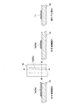
次に、ELパネル1において、駆動素子として用いられているスイッチトランジスタ5、駆動トランジスタ6などの薄膜トランジスタの製造方法について、図8〜図18に示す説明図を用いて説明する。
なお、図8から図18は、本発明における薄膜トランジスタの製造過程の一例を示す工程図である。この工程図は、図中平面図のA−A線に沿った断面部分と、図中平面図のB−B線に沿った断面部分と、同時に形成される走査線2と電圧供給線4の端子パッドTの断面部分を示す説明図であり、これらの図を参照して製造方法の概略を説明する。
また、この工程図(図8〜図18)で示す薄膜トランジスタは、スイッチトランジスタ5と駆動トランジスタ6とは一部形状が異なるが、スイッチトランジスタ5と駆動トランジスタ6に共通する概念的な薄膜トランジスタとして説明する。
Next, a method for manufacturing thin film transistors such as the
8 to 18 are process diagrams showing an example of the manufacturing process of the thin film transistor according to the present invention. This process diagram shows a cross-sectional portion along the line AA in the plan view in the drawing, a cross-sectional portion along the line BB in the plan view in the drawing, and the
The thin film transistors shown in the process diagrams (FIGS. 8 to 18) are described as conceptual thin film transistors common to the
まず、基板10上にゲートメタル層をスパッタリングで堆積させ、フォトリソグラフィー法及びエッチング法等によってパターニングして、図8に示すように、ゲート電極5a(6a)を形成する。また、端子パッドT部分には、ゲート電極5a(6a)とともに、下層電極T1が形成される(ゲート電極形成工程)。
なお、ゲート電極5a(6a)とともに、信号線3、キャパシタ7の電極7aが形成されている(図5、図6参照)。
First, a gate metal layer is deposited on the
The
次いで、図9に示すように、プラズマCVDによって、窒化シリコン等の第二絶縁膜11、半導体膜5b(6b)となるアモルファスシリコン等の半導体層9b、チャネル保護膜と5d(6d)なる窒化シリコン等の保護絶縁膜9dを連続して堆積し、三層を成膜する(三層成膜工程)。
Next, as shown in FIG. 9, a second insulating
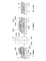
次いで、図10に示すように、フォトリソグラフィー法及びエッチング法等によって保護絶縁膜9dのパターニングを行い、半導体膜5b(6b)におけるチャネルとなる領域を覆うチャネル保護膜5d(6d)を形成する(保護膜形成工程)。
Next, as shown in FIG. 10, the protective
次いで、チャネル保護膜5d(6d)が形成された半導体層9b上に、図11に示すように、不純物半導体膜5f,5g(6f,6g)となる不純物半導体層9fを成膜する。
なお、p型TFTの場合、p+Siの不純物半導体層9fは、SiH4ガス中にジボラン等のアクセプター型の不純物を混入させてプラズマ成膜させることで形成する。また、n型TFTの場合、n+Siの不純物半導体層9fは、SiH4ガス中にアルシンやホスフィン等のドナー型の不純物を混入させてプラズマ成膜させることで形成する。
Next, as shown in FIG. 11, an
In the case of a p-type TFT, the p + Si
次いで、図12に示すように、フォトリソグラフィーによって不純物半導体層9f及び半導体層9bを連続してパターニングして、不純物半導体膜5f,5g(6f,6g)及び島状の半導体膜5b(6b)を形成する(半導体膜形成工程)。
なお、不純物半導体膜5f,5g(6f,6g)は、半導体膜5b(6b)上であってチャネル保護膜5d(6d)を挟んで対向する配置に形成されている。
Next, as shown in FIG. 12, the
Note that the
次いで、図13に示すように、端子パッドT部分における第二絶縁膜11をエッチングしてコンタクトホール11tを形成し、下層電極T1を露出させる(電極露出工程)。
Next, as shown in FIG. 13, the second insulating
次いで、図14に示すように、基板10上における不純物半導体膜5f,5g(6f,6g)と、チャネル保護膜5d(6d)と、半導体膜5b(6b)と、第二絶縁膜11とを覆う金属膜9hをスパッタリングで成膜する(金属膜成膜工程)。また、端子パッドT部分において、金属膜9hは、コンタクトホール11t内の下層電極T1上にも成膜されている。
なお、この金属膜成膜工程において、第二絶縁膜11とチャネル保護膜5d(6d)との間における半導体膜5b(6b)の端面が、スパッタリングによって成膜される金属膜9hと接触した部分が導電性を有するように変質してしまい、変質導電部5j(6j)が生成してしまうことがある。例えば、この変質導電部5j(6j)は、半導体膜5b(6b)中のシリコンが、導電性化合物であるシリサイドに変質した部分である。
この導電性化合物への変質について説明する。具体的に、例えば、400℃以上でアルミニウムとシリコンを接触させるとシリコン中にアルミニウムが拡散し、共融する性質があることが知られている。そして、金属膜成膜工程において、スパッタリングによって成膜される金属膜9hと接触した半導体膜5b(6b)の端面の定常的な温度は最高でも200℃程度であって、400℃を越えるような高温にはならないが、ターゲットから飛び出したスパッタ粒子の運動エネルギーは真空蒸着粒子の運動エネルギーと比べて100倍以上高くなっているため、半導体膜5b(6b)と衝突した瞬間のスパッタ粒子は極めて高温(例えば、400℃以上)であると考えられる。そのため、瞬間的にスパッタ粒子(アルミニウム)がシリコンと反応し、シリサイドなどの導電性化合物を作ってしまい、変質導電部5j(6j)が生成してしまうことがあるものと考えられる。
Next, as shown in FIG. 14, the
In this metal film formation step, the end surface of the
The alteration to the conductive compound will be described. Specifically, for example, it is known that when aluminum and silicon are brought into contact at 400 ° C. or higher, aluminum diffuses into silicon and eutectifies. In the metal film forming step, the steady temperature of the end face of the
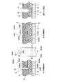
次いで、図15に示すように、フォトリソグラフィーによって金属膜9hをパターニングして、一対の不純物半導体膜5f,5g(6f,6g)上にソース電極5i(6i)及びドレイン電極5h(6h)を形成する(電極層形成工程)。このとき、図15に示すように、ソース電極5i(6i)とドレイン電極5h(6h)とが対向する方向と交差する方向において、チャネル保護膜5d(6d)及び半導体膜5b(6b)の端部が突出している。また、端子パッドT部分における金属膜9hはパターニングされて、下層電極T1上に上層電極T2が形成される。この下層電極T1と上層電極T2とが端子パッドTとなる。
なお、ソース電極5i(6i)及びドレイン電極5h(6h)とともに、走査線2、電圧供給線4、キャパシタ7の電極7bが形成されるようになっている。また、ソース電極5i(6i)及びドレイン電極5h(6h)の形成後に、画素電極8aが形成されるようになっている。
Next, as shown in FIG. 15, the
The
次いで、図16に示すように、ソース電極5i(6i)及びドレイン電極5h(6h)と、不純物半導体膜不純物半導体膜5f,5g(6f,6g)と、チャネル保護膜5d(6d)と、半導体膜5b(6b)、第二絶縁膜11とを覆う第一絶縁膜12を成膜する(オーバーコート工程)。なお、第一絶縁膜12は、第二絶縁膜11と同様に、プラズマCVDによって窒化シリコン等を成膜したものである。
更に、第一絶縁膜12上にフォトレジスト15を形成する。このフォトレジスト15における、ソース電極5i(6i)とドレイン電極5h(6h)とが対向する一の方向と交差する方向に突出したチャネル保護膜5d(6d)と、第一絶縁膜12との境界部分に対応する箇所に開口部15jが形成されている。また、フォトレジスト15における端子パッドT部分には開口部15tが形成されている。
なお、フォトレジスト15における画素電極8aに対応する部分にも開口部が形成されている。
Next, as shown in FIG. 16, a
Further, a
Note that an opening is also formed in a portion of the
次いで、図17に示すように、第一絶縁膜12における、ソース電極5i(6i)とドレイン電極5h(6h)とで覆われず、ソース電極5i(6i)とドレイン電極5h(6h)とが対向する一の方向と交差する方向に突出したチャネル保護膜5d(6d)と、第一絶縁膜12との境界部分をドライエッチングによりエッチングして、開口部12jを形成し、半導体膜5b(6b)の端部に相当する変質導電部5j(6j)の一部を露出させる(露出工程)。このとき、端子パッドT部分においては、上層電極T2上の第一絶縁膜12を同時にエッチングして開口部12tを形成し、上層電極T2の一部を露出させる。また、このとき、第一絶縁膜12における画素電極8aに対応する部分も同時にエッチングされて、画素電極8aが露出するようになっている。ここで、端子パッドT部分において上層電極T2上の第一絶縁膜12をエッチングする工程、及び、第一絶縁膜12における画素電極8aに対応する部分をエッチングする工程は、従来の製造方法においても存在する工程であり、開口部12jの形成は、これらのエッチング工程と同時に行うことができるため、ここまでの工程数が増加することはない。
Next, as shown in FIG. 17, the
次いで、図18に示すように、ドライエッチングの条件を、半導体膜をエッチングする条件に変更して、露出された半導体膜5b(6b)の端部に相当する変質導電部5j(6j)をドライエッチングによりエッチングして取り除く(端部除去工程)。なお、上記においては、開口部12jを形成する露出工程と変質導電部5j(6j)を取り除く(端部除去工程)とを別工程としたが、例えばドライエッチングの条件設定によって第一絶縁膜12のエッチングと半導体膜5b(6b)の端部の、変質導電部5j(6j)のエッチングを同時に行うことができる場合には、これらを1回の工程で行うようにしてもよい。
なお、変質導電部5j(6j)は、その少なくとも一部が取り除かれて、ソース電極5i(6i)とドレイン電極5h(6h)とが対向する一の方向に分断されていればよい。そして、変質導電部5j(6j)が分断されたことにより、半導体膜5b(6b)の端面に沿ったソース−ドレイン間のリーク電流経路を遮断するようになっている。
Next, as shown in FIG. 18, the dry etching condition is changed to the condition for etching the semiconductor film, and the altered
It should be noted that at least a part of the altered
こうして、半導体膜5b(6b)の端部が導電性を有するように変質してしまった変質導電部5j(6j)の一部をエッチングにより取り除き、リーク電流経路を遮断することで、一層のリーク電流の低減を図った薄膜トランジスタ(スイッチトランジスタ5、駆動トランジスタ6)が製造される。
In this way, a part of the altered
そして、フォトレジスト15を除去した後の第一絶縁膜12上にポリイミド等の感光性樹脂を成膜してバンク13を形成し、バンク13の開口部13a内における画素電極8a上に正孔注入層8bと発光層8cとを成膜し、更に、対向電極8dを形成することによりEL素子8が構成され、ELパネル1が製造される(図5参照)。
なお、図7に示したように、変質導電部5j(6j)の少なくとも一部を取り除くべく、リーク電流経路を遮断するために形成した開口部12j内には、バンク13を構成する部材が充填されるようになっているため、第一絶縁膜12上にバンク13が安定して配されている。
Then, a photosensitive resin such as polyimide is formed on the first insulating
In addition, as shown in FIG. 7, in order to remove at least a part of the altered
このように、ELパネル1において、駆動素子として用いられているスイッチトランジスタ5、駆動トランジスタ6などの薄膜トランジスタは、その半導体膜5b(6b)の端部が導電性を有するように変質してしまった変質導電部5j(6j)の一部を取り除くことで、半導体膜5b(6b)の端面に沿ったソース−ドレイン間のリーク電流経路を遮断しているので、より一層のリーク電流の低減が図られている。
そして、リーク電流の低減が図られた薄膜トランジスタを駆動素子(スイッチトランジスタ5、駆動トランジスタ6)としているELパネル1は、表示画質の向上が図られるので、良好な画像表示が可能になる。
As described above, in the
The
また、薄膜トランジスタにリーク電流があったときに、そのリーク電流を無くすことができた場合、ELパネルでも液晶パネルでも、それによる特性改善効果は少なからずあるが、ELパネルの方がリーク電流の低減による表示画質向上の効果は大きいものと考えられる。
これは、液晶パネルの場合、液晶素子そのものが容量性を有しており、階調信号電圧に応じた電荷を、駆動トランジスタを介して保持容量Cs及び液晶容量Clcに保持することによって階調制御するため、駆動トランジスタをなす薄膜トランジスタにリーク電流があっても、顕著には影響しない。
これに対し、ELパネルでは、駆動トランジスタのゲートに階調信号電圧を印加することによりソース・ドレイン間に流れる電流を制御することによって階調を制御するため、駆動トランジスタをなす薄膜トランジスタにリーク電流があると、階調制御に顕著に影響が生じる。このように、ELパネルは液晶パネルより、薄膜トランジスタのリーク電流の影響を受け易いのである。
よって、本発明をELパネルにおいて駆動素子として用いられる薄膜トランジスタに適用することは、表示画質向上のうえで有用であるといえる。
In addition, when there is a leakage current in the thin film transistor, if the leakage current can be eliminated, the EL panel and the liquid crystal panel have a considerable effect on improving the characteristics, but the EL panel reduces the leakage current. It is considered that the effect of improving the display image quality due to is great.
This is because, in the case of a liquid crystal panel, the liquid crystal element itself has capacitance, and gradation control is performed by holding charges corresponding to the gradation signal voltage in the storage capacitor Cs and the liquid crystal capacitor Clc via the drive transistor. Therefore, even if there is a leakage current in the thin film transistor that constitutes the driving transistor, there is no significant influence.
On the other hand, in the EL panel, since the gradation is controlled by controlling the current flowing between the source and the drain by applying the gradation signal voltage to the gate of the driving transistor, there is a leakage current in the thin film transistor forming the driving transistor. If so, the gradation control is significantly affected. Thus, the EL panel is more susceptible to the leakage current of the thin film transistor than the liquid crystal panel.
Therefore, it can be said that application of the present invention to a thin film transistor used as a driving element in an EL panel is useful in improving display image quality.
なお、本発明の適用は上述した実施形態に限定されることなく、本発明の趣旨を逸脱しない範囲で適宜変更可能である。 The application of the present invention is not limited to the above-described embodiment, and can be appropriately changed without departing from the spirit of the present invention.
1 ELパネル
5 スイッチトランジスタ(薄膜トランジスタ)
6 駆動トランジスタ(薄膜トランジスタ)
5a、6a ゲート電極
5b、6b 半導体膜
5d、6d チャネル保護膜(保護膜)
5f、6f 不純物半導体膜
5g、6g 不純物半導体膜
5h、6h ドレイン電極
5i、6i ソース電極
5j、6j 変質導電部
8 EL素子
9b 半導体層
9d 保護絶縁膜
9f 不純物半導体層
9h 金属膜
10 基板
11 第二絶縁膜
12 第一絶縁膜
12j コンタクトホール
12t コンタクトホール
13 バンク
15 フォトレジスト
15j 開口部
15t 開口部
T1 下層電極
T2 上層電極
T 端子パッド
1
6 Drive transistor (thin film transistor)
5a,
5f, 6f
Claims (6)
前記半導体層をパターニングして島状の形状を有する半導体膜を形成する半導体膜形成工程と、
前記基板上における前記半導体膜の側面に接して該半導体膜を覆う金属膜を成膜する金属膜成膜工程と、
前記金属膜をパターニングして、前記半導体膜上に電極層を形成し、該電極層より前記半導体膜の端部を突出させる電極層形成工程と、
前記電極層及び前記半導体膜を覆う第一絶縁膜を成膜するオーバーコート工程と、
前記第一絶縁膜の、前記電極層から突出した前記半導体膜の端部の側面と前記第一絶縁膜との境界部分の一部に対応する箇所に開口部を形成して、前記半導体膜の端部の一部を露出させる露出工程と、
露出された前記半導体膜の端部の一部を、前記開口部を介してエッチングして取り除く端部除去工程と、
を備えることを特徴とする薄膜トランジスタの製造方法。 A semiconductor layer forming step of forming a semiconductor layer containing silicon on the upper surface side of the substrate;
A semiconductor film forming step of patterning the semiconductor layer to form an island-shaped semiconductor film;
A metal film forming step of forming a metal film in contact with a side surface of the semiconductor film on the substrate and covering the semiconductor film;
Patterning the metal film, forming an electrode layer on the semiconductor film, and forming an electrode layer projecting an end of the semiconductor film from the electrode layer;
An overcoat step of forming a first insulating film covering the electrode layer and the semiconductor film;
Forming an opening in a portion of the first insulating film corresponding to a part of a boundary portion between the side surface of the end of the semiconductor film protruding from the electrode layer and the first insulating film; An exposure process for exposing a part of the end; and
An edge removing step of removing a part of the exposed edge of the semiconductor film by etching through the opening;
A method for producing a thin film transistor, comprising:
前記端部除去工程は、前記半導体膜の前記導電性化合物に変質した領域の一部を取り除くことを特徴とする請求項1に記載の薄膜トランジスタの製造方法。 In the exposing step, the semiconductor film is formed along the side surface of the semiconductor film in contact with the metal film at the time of forming the metal film in the metal film forming step at the end of the semiconductor film. Expose part of the area transformed into a conductive compound,
2. The method of manufacturing a thin film transistor according to claim 1, wherein the edge removing step removes a part of a region of the semiconductor film that has changed into the conductive compound. 3.
前記半導体膜形成工程の後に、前記保護絶縁膜をパターニングして、前記半導体層におけるチャネルとなる領域を覆う保護膜を形成する保護膜形成工程を備え、
前記半導体膜形成工程は、前記保護膜が形成された前記半導体層上に、不純物半導体層を成膜し、前記不純物半導体層をパターニングして、前記保護膜を挟んで対向する一対の不純物半導体膜を形成する不純物半導体膜形成工程を含み、
前記金属膜成膜工程は、前記金属膜を前記不純物半導体膜と前記保護膜と前記半導体膜の側面に接して該半導体膜を覆うように成膜する工程を含み、
前記電極層形成工程は、前記金属膜をパターニングして、前記一対の不純物半導体膜上にソース電極及びドレイン電極を形成する工程を含むことを特徴とする請求項2に記載の薄膜トランジスタの製造方法。 The semiconductor layer forming step includes a step of forming a protective insulating film on the semiconductor layer,
After the semiconductor film forming step, the protective insulating film is patterned to form a protective film forming step of forming a protective film that covers a region to be a channel in the semiconductor layer,
In the semiconductor film forming step, an impurity semiconductor layer is formed on the semiconductor layer on which the protective film is formed, the impurity semiconductor layer is patterned, and a pair of impurity semiconductor films facing each other with the protective film interposed therebetween Including an impurity semiconductor film forming step of forming
The metal film forming step includes a step of forming the metal film so as to contact the side surfaces of the impurity semiconductor film, the protective film, and the semiconductor film and cover the semiconductor film,
3. The method of manufacturing a thin film transistor according to claim 2, wherein the electrode layer forming step includes a step of patterning the metal film to form a source electrode and a drain electrode on the pair of impurity semiconductor films.
前記半導体層形成工程は、前記基板の上面に、前記ゲート電極形成工程により形成された前記ゲート電極及び前記下層電極を覆って第二絶縁膜を成膜する工程と、該第二絶縁膜上に前記半導体層を形成する工程と、を含み、
前記半導体膜形成工程の後に、端子パッド部において、前記第二絶縁膜をエッチングして、前記下層電極を露出させる電極露出工程を備え、
前記金属膜成膜工程は、前記金属膜を前記第二絶縁膜上及び前記露出された下層電極上に成膜する工程を含み、
前記電極層形成工程は、前記端子パッド部において、前記電極層の形成と同時に、前記露出された下層電極上の前記金属膜をパターニングして、前記露出された下層電極上に上層電極を形成する工程を含み、
前記オーバーコート工程は、前記第一絶縁膜を前記上層電極も覆うように成膜し、
前記露出工程は、前記端子パッド部において、前記開口部の形成と同時に、前記上層電極上の前記第一絶縁膜をエッチングして、該上層電極の少なくとも一部を露出させる工程を含むことを特徴とする請求項3に記載の薄膜トランジスタの製造方法。 Before the semiconductor layer forming step, a gate electrode forming step of forming a gate electrode and a lower layer electrode on the upper surface of the substrate,
The semiconductor layer forming step includes: forming a second insulating film on the upper surface of the substrate so as to cover the gate electrode and the lower layer electrode formed in the gate electrode forming step; Forming the semiconductor layer, and
After the semiconductor film forming step, the terminal pad portion includes an electrode exposing step of etching the second insulating film to expose the lower layer electrode,
The metal film deposition step includes the step of depositing the metal film on the second insulating film and the exposed lower electrode,
The electrode layer forming step forms the upper layer electrode on the exposed lower layer electrode by patterning the metal film on the exposed lower layer electrode simultaneously with the formation of the electrode layer in the terminal pad portion. Including steps,
In the overcoat step, the first insulating film is formed so as to cover the upper electrode,
The exposing step includes a step of exposing at least a part of the upper layer electrode by etching the first insulating film on the upper layer electrode simultaneously with the formation of the opening in the terminal pad portion. A method for producing a thin film transistor according to claim 3.
金属膜からなり、前記半導体膜の上部に、該半導体膜の端部を突出させた形状に形成された電極層と、
前記電極層及び前記半導体膜を覆う第一絶縁膜と、
前記第一絶縁膜上に形成された隔壁と、
を備え、
前記半導体膜は、前記端部において、該半導体膜の一部が取り除かれた切り欠き部を有し、該切り欠き部において、前記電極層をなす前記金属膜の形成時に前記半導体膜が前記金属膜と接触して、前記半導体膜の側面に沿って形成された導電性化合物に変質した領域が分断され、
前記第一絶縁膜は、前記切り欠き部に対応する位置に形成された開口部を有し、
前記開口部に、前記隔壁を形成する材料が充填されていることを特徴とする薄膜トランジスタ。 A semiconductor film containing silicon formed in an island shape on the upper surface side of the substrate;
An electrode layer made of a metal film and formed on the upper part of the semiconductor film in a shape in which an end of the semiconductor film protrudes;
A first insulating film covering the electrode layer and the semiconductor film;
A partition formed on the first insulating film;
With
The semiconductor film has a cutout portion from which a part of the semiconductor film is removed at the end portion, and the semiconductor film is formed of the metal film when forming the metal film forming the electrode layer in the cutout portion. In contact with the film, a region transformed into a conductive compound formed along the side surface of the semiconductor film is divided ,
The first insulating film has an opening formed at a position corresponding to the notch,
A thin film transistor , wherein the opening is filled with a material for forming the partition .
前記半導体膜上に、前記保護膜を挟んで対向する位置に形成された一対の不純物半導体膜と、
を備え、
前記電極層は、前記一対の不純物半導体膜上に形成されて、ソース電極及びドレイン電極をなし、
前記第一絶縁膜は、前記ソース電極及びドレイン電極と前記不純物半導体膜と前記保護膜と前記半導体膜を覆っていることを特徴とする請求項5に記載の薄膜トランジスタ。 A protective film made of a protective insulating film formed on a region to be a channel of the semiconductor film;
On the semiconductor film, a pair of impurity semiconductor films formed at positions facing each other with the protective film interposed therebetween,
With
The electrode layer is formed on the pair of impurity semiconductor films to form a source electrode and a drain electrode,
6. The thin film transistor according to claim 5 , wherein the first insulating film covers the source and drain electrodes, the impurity semiconductor film, the protective film, and the semiconductor film.
Priority Applications (1)
| Application Number | Priority Date | Filing Date | Title |
|---|---|---|---|
| JP2009054624A JP5428404B2 (en) | 2009-03-09 | 2009-03-09 | THIN FILM TRANSISTOR AND METHOD FOR PRODUCING THIN FILM TRANSISTOR |
Applications Claiming Priority (1)
| Application Number | Priority Date | Filing Date | Title |
|---|---|---|---|
| JP2009054624A JP5428404B2 (en) | 2009-03-09 | 2009-03-09 | THIN FILM TRANSISTOR AND METHOD FOR PRODUCING THIN FILM TRANSISTOR |
Publications (3)
| Publication Number | Publication Date |
|---|---|
| JP2010212328A JP2010212328A (en) | 2010-09-24 |
| JP2010212328A5 JP2010212328A5 (en) | 2011-11-17 |
| JP5428404B2 true JP5428404B2 (en) | 2014-02-26 |
Family
ID=42972227
Family Applications (1)
| Application Number | Title | Priority Date | Filing Date |
|---|---|---|---|
| JP2009054624A Expired - Fee Related JP5428404B2 (en) | 2009-03-09 | 2009-03-09 | THIN FILM TRANSISTOR AND METHOD FOR PRODUCING THIN FILM TRANSISTOR |
Country Status (1)
| Country | Link |
|---|---|
| JP (1) | JP5428404B2 (en) |
Families Citing this family (2)
| Publication number | Priority date | Publication date | Assignee | Title |
|---|---|---|---|---|
| KR101348537B1 (en) * | 2010-09-29 | 2014-01-07 | 파나소닉 주식회사 | El display panel, el display device and method for manufacturing el display panel |
| CN102576722B (en) * | 2010-09-29 | 2015-05-27 | 株式会社日本有机雷特显示器 | EL display panel, EL display apparatus, and method of manufacturing EL display panel |
Family Cites Families (7)
| Publication number | Priority date | Publication date | Assignee | Title |
|---|---|---|---|---|
| JP3412277B2 (en) * | 1994-08-23 | 2003-06-03 | カシオ計算機株式会社 | Thin film transistor and method of manufacturing the same |
| JP3865818B2 (en) * | 1996-04-16 | 2007-01-10 | 三菱電機株式会社 | Manufacturing method of active matrix substrate |
| JP3801687B2 (en) * | 1996-06-06 | 2006-07-26 | 三菱電機株式会社 | Thin film transistor and method for manufacturing the same |
| JP3323889B2 (en) * | 1996-10-28 | 2002-09-09 | 三菱電機株式会社 | Method for manufacturing thin film transistor |
| JPH10270701A (en) * | 1997-03-27 | 1998-10-09 | Advanced Display:Kk | Thin film transistor and its production |
| JP2000214485A (en) * | 1999-01-21 | 2000-08-04 | Toshiba Corp | Array substrate and liquid crystal display elements |
| JP5212683B2 (en) * | 2007-03-20 | 2013-06-19 | カシオ計算機株式会社 | Transistor panel and manufacturing method thereof |
-
2009
- 2009-03-09 JP JP2009054624A patent/JP5428404B2/en not_active Expired - Fee Related
Also Published As
| Publication number | Publication date |
|---|---|
| JP2010212328A (en) | 2010-09-24 |
Similar Documents
| Publication | Publication Date | Title |
|---|---|---|
| KR101432110B1 (en) | Organic light emitting display and method for manufacturing the same | |
| KR101298309B1 (en) | Transistor structure, manufacturing method of transistor structure, and light emitting apparatus | |
| KR20100001597A (en) | Display device and manufacturing method thereof | |
| KR101272373B1 (en) | Transistor structure and light emitting apparatus | |
| JP4973698B2 (en) | THIN FILM TRANSISTOR AND METHOD FOR PRODUCING THIN FILM TRANSISTOR | |
| JP5428404B2 (en) | THIN FILM TRANSISTOR AND METHOD FOR PRODUCING THIN FILM TRANSISTOR | |
| JP2012064604A (en) | Transistor structure, method of manufacturing transistor structure, and light-emitting device | |
| JP2011014358A (en) | Method and device for manufacturing light-emitting panel | |
| JP5630170B2 (en) | Method for manufacturing transistor structure | |
| JP5481998B2 (en) | Method for manufacturing transistor | |
| WO2004051703A2 (en) | Organic electroluminescence display panel and manufacturing method thereof | |
| JP5136616B2 (en) | Transistor structure, method for manufacturing transistor structure, and light emitting device | |
| JP5471564B2 (en) | THIN FILM TRANSISTOR AND METHOD FOR PRODUCING THIN FILM TRANSISTOR | |
| JP2012069540A (en) | Thin film transistor, manufacturing method for thin film transistor, and light-emitting device | |
| JP5205634B2 (en) | Transistor structure, method for manufacturing transistor structure, and light emitting device | |
| JP2012019120A (en) | Transistor structure, method for manufacturing transistor structure, and light emitting device | |
| JP5532908B2 (en) | THIN FILM TRANSISTOR AND METHOD FOR PRODUCING THIN FILM TRANSISTOR | |
| JP5381414B2 (en) | Light emitting panel manufacturing method and light emitting panel manufacturing apparatus | |
| JP5533070B2 (en) | THIN FILM TRANSISTOR, LIGHT EMITTING DEVICE, AND METHOD FOR PRODUCING THIN FILM TRANSISTOR | |
| JP5458770B2 (en) | Transistor and transistor manufacturing method | |
| JP5630169B2 (en) | Method for manufacturing transistor structure | |
| JP5152115B2 (en) | Light emitting panel manufacturing method and light emitting panel manufacturing apparatus | |
| JP2011048215A (en) | Transistor substrate and light emitting device | |
| JP2011181551A (en) | Thin film transistor and method of manufacturing thin film transistor | |
| JP2012019122A (en) | Transistor structure, method for manufacturing transistor structure, and light emitting device |
Legal Events
| Date | Code | Title | Description |
|---|---|---|---|
| A521 | Request for written amendment filed |
Free format text: JAPANESE INTERMEDIATE CODE: A523 Effective date: 20110930 |
|
| A621 | Written request for application examination |
Free format text: JAPANESE INTERMEDIATE CODE: A621 Effective date: 20110930 |
|
| RD02 | Notification of acceptance of power of attorney |
Free format text: JAPANESE INTERMEDIATE CODE: A7422 Effective date: 20110930 |
|
| A977 | Report on retrieval |
Free format text: JAPANESE INTERMEDIATE CODE: A971007 Effective date: 20130731 |
|
| A131 | Notification of reasons for refusal |
Free format text: JAPANESE INTERMEDIATE CODE: A131 Effective date: 20130806 |
|
| A521 | Request for written amendment filed |
Free format text: JAPANESE INTERMEDIATE CODE: A523 Effective date: 20131007 |
|
| TRDD | Decision of grant or rejection written | ||
| A01 | Written decision to grant a patent or to grant a registration (utility model) |
Free format text: JAPANESE INTERMEDIATE CODE: A01 Effective date: 20131105 |
|
| A61 | First payment of annual fees (during grant procedure) |
Free format text: JAPANESE INTERMEDIATE CODE: A61 Effective date: 20131118 |
|
| R150 | Certificate of patent or registration of utility model |
Free format text: JAPANESE INTERMEDIATE CODE: R150 |
|
| LAPS | Cancellation because of no payment of annual fees |