JP5428038B2 - Metal-polymer hybrid nanomaterial, method for producing the same, method for adjusting optical properties of metal-polymer hybrid nanomaterial, and optoelectronic device using the same - Google Patents
Metal-polymer hybrid nanomaterial, method for producing the same, method for adjusting optical properties of metal-polymer hybrid nanomaterial, and optoelectronic device using the same Download PDFInfo
- Publication number
- JP5428038B2 JP5428038B2 JP2009534518A JP2009534518A JP5428038B2 JP 5428038 B2 JP5428038 B2 JP 5428038B2 JP 2009534518 A JP2009534518 A JP 2009534518A JP 2009534518 A JP2009534518 A JP 2009534518A JP 5428038 B2 JP5428038 B2 JP 5428038B2
- Authority
- JP
- Japan
- Prior art keywords
- metal
- nanotube
- polymer hybrid
- p3mt
- nanomaterial
- Prior art date
- Legal status (The legal status is an assumption and is not a legal conclusion. Google has not performed a legal analysis and makes no representation as to the accuracy of the status listed.)
- Expired - Fee Related
Links
Images


Classifications
-
- B—PERFORMING OPERATIONS; TRANSPORTING
- B82—NANOTECHNOLOGY
- B82B—NANOSTRUCTURES FORMED BY MANIPULATION OF INDIVIDUAL ATOMS, MOLECULES, OR LIMITED COLLECTIONS OF ATOMS OR MOLECULES AS DISCRETE UNITS; MANUFACTURE OR TREATMENT THEREOF
- B82B3/00—Manufacture or treatment of nanostructures by manipulation of individual atoms or molecules, or limited collections of atoms or molecules as discrete units
-
- C—CHEMISTRY; METALLURGY
- C09—DYES; PAINTS; POLISHES; NATURAL RESINS; ADHESIVES; COMPOSITIONS NOT OTHERWISE PROVIDED FOR; APPLICATIONS OF MATERIALS NOT OTHERWISE PROVIDED FOR
- C09K—MATERIALS FOR MISCELLANEOUS APPLICATIONS, NOT PROVIDED FOR ELSEWHERE
- C09K11/00—Luminescent, e.g. electroluminescent, chemiluminescent materials
- C09K11/06—Luminescent, e.g. electroluminescent, chemiluminescent materials containing organic luminescent materials
-
- H—ELECTRICITY
- H01—ELECTRIC ELEMENTS
- H01B—CABLES; CONDUCTORS; INSULATORS; SELECTION OF MATERIALS FOR THEIR CONDUCTIVE, INSULATING OR DIELECTRIC PROPERTIES
- H01B1/00—Conductors or conductive bodies characterised by the conductive materials; Selection of materials as conductors
- H01B1/06—Conductors or conductive bodies characterised by the conductive materials; Selection of materials as conductors mainly consisting of other non-metallic substances
- H01B1/12—Conductors or conductive bodies characterised by the conductive materials; Selection of materials as conductors mainly consisting of other non-metallic substances organic substances
-
- H—ELECTRICITY
- H10—SEMICONDUCTOR DEVICES; ELECTRIC SOLID-STATE DEVICES NOT OTHERWISE PROVIDED FOR
- H10K—ORGANIC ELECTRIC SOLID-STATE DEVICES
- H10K50/00—Organic light-emitting devices
- H10K50/10—OLEDs or polymer light-emitting diodes [PLED]
- H10K50/11—OLEDs or polymer light-emitting diodes [PLED] characterised by the electroluminescent [EL] layers
-
- H—ELECTRICITY
- H10—SEMICONDUCTOR DEVICES; ELECTRIC SOLID-STATE DEVICES NOT OTHERWISE PROVIDED FOR
- H10K—ORGANIC ELECTRIC SOLID-STATE DEVICES
- H10K71/00—Manufacture or treatment specially adapted for the organic devices covered by this subclass
- H10K71/10—Deposition of organic active material
- H10K71/12—Deposition of organic active material using liquid deposition, e.g. spin coating
- H10K71/125—Deposition of organic active material using liquid deposition, e.g. spin coating using electrolytic deposition e.g. in-situ electropolymerisation
-
- H—ELECTRICITY
- H10—SEMICONDUCTOR DEVICES; ELECTRIC SOLID-STATE DEVICES NOT OTHERWISE PROVIDED FOR
- H10K—ORGANIC ELECTRIC SOLID-STATE DEVICES
- H10K85/00—Organic materials used in the body or electrodes of devices covered by this subclass
- H10K85/10—Organic polymers or oligomers
- H10K85/111—Organic polymers or oligomers comprising aromatic, heteroaromatic, or aryl chains, e.g. polyaniline, polyphenylene or polyphenylene vinylene
- H10K85/113—Heteroaromatic compounds comprising sulfur or selene, e.g. polythiophene
-
- B—PERFORMING OPERATIONS; TRANSPORTING
- B82—NANOTECHNOLOGY
- B82Y—SPECIFIC USES OR APPLICATIONS OF NANOSTRUCTURES; MEASUREMENT OR ANALYSIS OF NANOSTRUCTURES; MANUFACTURE OR TREATMENT OF NANOSTRUCTURES
- B82Y40/00—Manufacture or treatment of nanostructures
-
- C—CHEMISTRY; METALLURGY
- C09—DYES; PAINTS; POLISHES; NATURAL RESINS; ADHESIVES; COMPOSITIONS NOT OTHERWISE PROVIDED FOR; APPLICATIONS OF MATERIALS NOT OTHERWISE PROVIDED FOR
- C09K—MATERIALS FOR MISCELLANEOUS APPLICATIONS, NOT PROVIDED FOR ELSEWHERE
- C09K2211/00—Chemical nature of organic luminescent or tenebrescent compounds
- C09K2211/14—Macromolecular compounds
-
- Y—GENERAL TAGGING OF NEW TECHNOLOGICAL DEVELOPMENTS; GENERAL TAGGING OF CROSS-SECTIONAL TECHNOLOGIES SPANNING OVER SEVERAL SECTIONS OF THE IPC; TECHNICAL SUBJECTS COVERED BY FORMER USPC CROSS-REFERENCE ART COLLECTIONS [XRACs] AND DIGESTS
- Y02—TECHNOLOGIES OR APPLICATIONS FOR MITIGATION OR ADAPTATION AGAINST CLIMATE CHANGE
- Y02E—REDUCTION OF GREENHOUSE GAS [GHG] EMISSIONS, RELATED TO ENERGY GENERATION, TRANSMISSION OR DISTRIBUTION
- Y02E10/00—Energy generation through renewable energy sources
- Y02E10/50—Photovoltaic [PV] energy
- Y02E10/549—Organic PV cells
-
- Y—GENERAL TAGGING OF NEW TECHNOLOGICAL DEVELOPMENTS; GENERAL TAGGING OF CROSS-SECTIONAL TECHNOLOGIES SPANNING OVER SEVERAL SECTIONS OF THE IPC; TECHNICAL SUBJECTS COVERED BY FORMER USPC CROSS-REFERENCE ART COLLECTIONS [XRACs] AND DIGESTS
- Y10—TECHNICAL SUBJECTS COVERED BY FORMER USPC
- Y10T—TECHNICAL SUBJECTS COVERED BY FORMER US CLASSIFICATION
- Y10T428/00—Stock material or miscellaneous articles
- Y10T428/29—Coated or structually defined flake, particle, cell, strand, strand portion, rod, filament, macroscopic fiber or mass thereof
- Y10T428/2913—Rod, strand, filament or fiber
- Y10T428/2933—Coated or with bond, impregnation or core
- Y10T428/2935—Discontinuous or tubular or cellular core
Landscapes
- Engineering & Computer Science (AREA)
- Chemical & Material Sciences (AREA)
- Materials Engineering (AREA)
- Physics & Mathematics (AREA)
- Manufacturing & Machinery (AREA)
- Optics & Photonics (AREA)
- Spectroscopy & Molecular Physics (AREA)
- Organic Chemistry (AREA)
- Nanotechnology (AREA)
- Crystallography & Structural Chemistry (AREA)
- Electroluminescent Light Sources (AREA)
- Compositions Of Macromolecular Compounds (AREA)
- Luminescent Compositions (AREA)
- Coating Of Shaped Articles Made Of Macromolecular Substances (AREA)
- Polyoxymethylene Polymers And Polymers With Carbon-To-Carbon Bonds (AREA)
Description
本発明は、金属−高分子ハイブリッドナノ物質に係り、より詳細には、有機発光高分子と金属とを含んで形成されたハイブリッドナノ物質、その製造方法、該金属−高分子ハイブリッドナノ物質の光学特性の調節方法及びそれを利用した光電子素子に関する。 The present invention relates to a metal-polymer hybrid nanomaterial, and more particularly, a hybrid nanomaterial formed by including an organic light emitting polymer and a metal, a method for producing the same, and an optical property of the metal-polymer hybrid nanomaterial. The present invention relates to a characteristic adjusting method and an optoelectronic device using the same.
有機ナノ物質についての研究は、Martinグループを初めとして主に電気的特性に優れたナノ物質を用いて合成し、その特性を確認することである。そして、電気的特性を調節してナノトランジスタを製作し、ナノバイオセンサー、化学センサー及び電気変色素子などを製作し、その特性研究に焦点を合わせた。代表的な発光高分子ナノ物質であるPoly(p−phenylenevinylene)(PPV)を化学気相蒸着方法を用いて成長させ、その特性観察を初めとして多くの研究がなされている。 Research on organic nanomaterials is to synthesize using nanomaterials with excellent electrical properties, starting with the Martin group, and confirm their properties. Then, the nano-transistors were fabricated by adjusting the electrical characteristics, and nano-biosensors, chemical sensors, electrochromic elements, etc. were fabricated, focusing on the research on the characteristics. A large amount of research has been conducted, starting with the observation of the characteristics of poly (p-phenylenevinylene) (PPV), which is a typical light-emitting polymer nanomaterial, grown using chemical vapor deposition.
ナノ素材として、最近多くの研究が進められているのが、炭素ナノチューブ(CNT)である。炭素ナノチューブは、機械的、電気的、化学的特性などにおいて、今までの如何なる素材より優れた性質を示しており、そのサイズ面でも、電気、電子素子特性によく合う。それで、メモリ素子、FED(Field Emission Display)などに対する利用が活発に研究されている。しかし、炭素ナノチューブは、製作過程で高温を保持しなければならず、ナノチューブの成長及び精製過程が非常に複雑でコスト高となるという短所がある。また、ナノチューブが、単一壁(single−wall)チューブであるか、多重壁(multi−wall)チューブであるかによって物理的、化学的性質に差があり、ナノチューブの直径及び電気的性質を調節することが非常に難しく、加工性が劣悪であるという問題点がある。 As a nanomaterial, carbon nanotubes (CNT) have been studied a lot recently. Carbon nanotubes exhibit properties superior to any conventional materials in terms of mechanical, electrical, chemical properties, etc., and they are well suited to electrical and electronic device characteristics in terms of their size. Thus, the use of memory devices, field emission displays (FEDs), and the like has been actively researched. However, carbon nanotubes have to be maintained at a high temperature during the production process, and the nanotube growth and purification process is very complicated and expensive. Also, there are differences in physical and chemical properties depending on whether the nanotube is a single-wall tube or a multi-wall tube, and the diameter and electrical properties of the nanotube are controlled. There is a problem that it is very difficult to do and the workability is poor.
最近、有機高分子と無機半導体及び金属の複合構造を成す新たな形態の物質とを製作して、既存の有機物質が有している特性より優れた特性を示し、多様な分野で応用可能性が報告されている。有機高分子としては、π共役高分子を例として挙げられる、π共役高分子は、高分子の機械的特性を有しながらも、化学的ドーピングを通じて絶縁体から半導体または導体に転移するために、電気、電子、光学素子などに応用されうる。最近、伝導性高分子は、2次電池、静電気防止、スイッチング素子、非線形素子、蓄電器、光記録材、電磁気波遮蔽材など実生活及び先端産業分野で応用されている。 Recently, we have fabricated organic polymers and new forms of materials that form a composite structure of inorganic semiconductors and metals, which show properties superior to those of existing organic materials and can be applied in various fields. Has been reported. As an organic polymer, a π-conjugated polymer can be cited as an example. A π-conjugated polymer has mechanical properties of a polymer, but is transferred from an insulator to a semiconductor or a conductor through chemical doping. It can be applied to electric, electronic, optical elements and the like. Recently, conductive polymers have been applied in real life and advanced industrial fields such as secondary batteries, antistatic, switching elements, nonlinear elements, capacitors, optical recording materials, and electromagnetic wave shielding materials.
π共役高分子ナノ物質についての研究は、伝導性高分子について活発に研究されており、発光ナノ物質についての研究はあまり多くないが、これはナノ構造の発光強度が弱くて発光特性の観察が難しく、発光ナノ物質が大気中に露出されれば、変形しやすくて、有機発光素子としての応用に多くの難点があるためである。 Research on π-conjugated polymer nanomaterials has been actively conducted on conductive polymers, and not much research has been done on luminescent nanomaterials. This is because if the luminescent nanomaterial is exposed to the atmosphere, it is easily deformed and has many difficulties in application as an organic light emitting device.
本発明が解決しようとする第1の課題は、発光強度が著しく増大し、ナノ光電子素子に応用可能な金属−高分子ハイブリッドナノ物質を提供することである。 The first problem to be solved by the present invention is to provide a metal-polymer hybrid nanomaterial that has a significantly increased emission intensity and can be applied to nano-optoelectronic devices.
本発明が解決しようとする第2の課題は、前記金属−高分子ハイブリッドナノ物質の製造方法を提供することである。 The second problem to be solved by the present invention is to provide a method for producing the metal-polymer hybrid nanomaterial.
本発明が解決しようとする第3の課題は、前記金属−高分子ハイブリッドナノ物質の光学特性の調節方法を提供することである。 The third problem to be solved by the present invention is to provide a method for adjusting the optical properties of the metal-polymer hybrid nanomaterial.
本発明が解決しようとする第4の課題は、前記金属−高分子ハイブリッドナノ物質を利用した光電素子を提供することである。 The fourth problem to be solved by the present invention is to provide a photoelectric device using the metal-polymer hybrid nanomaterial.
本発明は、前記第1の課題を解決するために、π共役構造の発光高分子を含むナノチューブまたはナノワイヤと、前記ナノチューブの内外部または前記ナノワイヤの外部に、前記ナノチューブまたはナノワイヤのエネルギーバンドギャップと類似したサイズの表面プラズモンエネルギー準位を有する金属からなる金属層と、を含む金属−高分子ハイブリッドナノ物質を提供する。 In order to solve the first problem, the present invention provides a nanotube or nanowire containing a light-emitting polymer having a π-conjugated structure, and an energy band gap of the nanotube or nanowire inside or outside the nanotube or outside the nanowire. A metal-polymer hybrid nanomaterial comprising a metal layer made of a metal having a surface plasmon energy level of a similar size is provided.
本発明の一実施例によれば、本発明による金属−高分子ハイブリッドナノ物質は、前記金属層の表面プラズモンエネルギー準位と前記ナノチューブまたはナノワイヤの伝導準位(conduction band)との間に表面プラズモン共鳴によるエネルギー伝達がなされることを特徴とする。 According to an embodiment of the present invention, the metal-polymer hybrid nanomaterial according to the present invention includes a surface plasmon between a surface plasmon energy level of the metal layer and a conduction level of the nanotube or nanowire. It is characterized by energy transfer by resonance.
また、前記π共役構造の発光高分子は、ドーパントによってドーピングされてナノチューブまたはナノワイヤのバンドギャップの間にバイポーラロンバンドを形成し、前記バイポーラロンバンドに存在する電子が表面プラズモン共鳴によって金属層のフェルミ準位に移動する電子伝達がなされることを特徴とする。 In addition, the light-emitting polymer having the π-conjugated structure is doped with a dopant to form a bipolaron band between the band gaps of the nanotubes or nanowires, and electrons existing in the bipolaron band are subjected to surface plasmon resonance so that the Fermi of the metal layer is formed. Electron transfer that moves to a level is performed.
本発明の他の実施例によれば、前記π共役構造の発光高分子は、ポリチオフェン、ポリ(3−アルキルチオフェン)、ポリ(3,4−エチレンジオキシチオフェン)、ポリピロール、ポリアニリン、ポリ(1,4−フェニレンビニレン)、ポリフェニレン及びこれらの誘導体からなる群から選択された一つ以上であり得る。
また、前記金属層は、銅(Cu)、ニッケル(Ni)、コバルト(Co)、鉄(Fe)、亜鉛(Zn)、チタン(Ti)、クロム(Cr)、銀(Ag)、金(Au)、白金(Pt)、アルミニウム(Al)、及びこれらの複合体からなる群から選択された一つ以上からなりうる。
According to another embodiment of the present invention, the π-conjugated structure light-emitting polymer may be polythiophene, poly (3-alkylthiophene), poly (3,4-ethylenedioxythiophene), polypyrrole, polyaniline, poly (1 , 4-phenylene vinylene), polyphenylene, and derivatives thereof.
The metal layer is made of copper (Cu), nickel (Ni), cobalt (Co), iron (Fe), zinc (Zn), titanium (Ti), chromium (Cr), silver (Ag), gold (Au ), Platinum (Pt), aluminum (Al), and a composite thereof.
一方、前記ドーパントは、カンポスルホン酸、ベンゼンスルホン酸、p−ドデシルベンゼンスルホン酸、テトラブチルアンモニウムヘキサフルオロホスフェート、テトラブチルアンモニウムテトラフルオロボレート、ナフタレンスルホン酸、ポリ(4−スチレンスルホン酸)、HC及びp−トルエンスルホン酸からなる群から選択された何れか一つ以上であり得る。 Meanwhile, the dopant includes camposulfonic acid, benzenesulfonic acid, p-dodecylbenzenesulfonic acid, tetrabutylammonium hexafluorophosphate, tetrabutylammonium tetrafluoroborate, naphthalenesulfonic acid, poly (4-styrenesulfonic acid), HC, and It may be any one or more selected from the group consisting of p-toluenesulfonic acid.
本発明のまた他の実施例によれば、前記金属層の厚さは、1ないし50nmであることが望ましい。 According to still another embodiment of the present invention, the thickness of the metal layer is preferably 1 to 50 nm.
本発明は、前記第2の課題を解決するために、(a)ナノサイズの気孔が形成されている多孔性テンプレートに電極として用いる金属を付着させる段階と、(b)極性溶媒、単量体、及びドーパントを含む混合液を撹拌して重合溶液を形成し、これを前記多孔性テンプレートのナノ気孔内で重合してπ共役構造の発光高分子を含むナノチューブまたはナノワイヤを形成する段階と、(c)前記ナノチューブの内外側または前記ナノワイヤの外側に、前記ナノチューブまたはナノワイヤのバンドギャップと類似したサイズの表面プラズモンバンドギャップを有する金属を電気化学的に蒸着して金属層を形成する段階と、(d)前記多孔性テンプレートを除去する段階と、を含む金属−高分子ハイブリッドナノ物質の製造方法を提供する。 In order to solve the second problem, the present invention includes (a) a step of attaching a metal used as an electrode to a porous template in which nano-sized pores are formed, and (b) a polar solvent and a monomer. And stirring the mixed solution containing the dopant to form a polymerization solution, which is polymerized in the nanopores of the porous template to form a nanotube or nanowire containing a π-conjugated structure light-emitting polymer; c) electrochemically depositing a metal having a surface plasmon band gap of a size similar to the band gap of the nanotube or nanowire on the inner or outer side of the nanotube or the outer side of the nanowire to form a metal layer; d) removing the porous template; and providing a method for producing a metal-polymer hybrid nanomaterial.
本発明の一実施例によれば、前記(b)段階で極性溶媒は、H2O、アセトニトリル及びN−メチルピロリジノンからなる群から選択された何れか一つ以上であり得る。
また、前記(b)段階で単量体は、チオフェン、3−メチルチオフェン、3−アルキルチオフェン、3,4−エチレンジオキシチオフェン、ピロール、アニリン、1,4−フェニレンビニレン、フェニレン及びその誘導体からなる群から選択された何れか一つ以上であり得る。
According to an embodiment of the present invention, the polar solvent in the step (b) may be any one or more selected from the group consisting of H 2 O, acetonitrile, and N-methylpyrrolidinone.
In the step (b), the monomer is selected from thiophene, 3-methylthiophene, 3-alkylthiophene, 3,4-ethylenedioxythiophene, pyrrole, aniline, 1,4-phenylenevinylene, phenylene and derivatives thereof. It may be any one or more selected from the group consisting of:
一方、前記(b)段階のドーパントは、カンポスルホン酸、ベンゼンスルホン酸、p−ドデシルベンゼンスルホン酸、テトラブチルアンモニウムヘキサフルオロホスフェート、テトラブチルアンモニウムテトラフルオロボレート、1−ブチル−3−メチルイミダゾリウムヘキサフルオロホスフェート、ナフタレンスルホン酸、ポリ(4−スチレンスルホン酸)、HCl及びp−トルエンスルホン酸からなる群から選択された何れか一つ以上であり得る。 On the other hand, the dopant in the step (b) is camposulfonic acid, benzenesulfonic acid, p-dodecylbenzenesulfonic acid, tetrabutylammonium hexafluorophosphate, tetrabutylammonium tetrafluoroborate, 1-butyl-3-methylimidazolium hexa It may be any one or more selected from the group consisting of fluorophosphate, naphthalenesulfonic acid, poly (4-styrenesulfonic acid), HCl and p-toluenesulfonic acid.
本発明の他の実施例によれば、前記(c)段階の金属は、銅(Cu)、ニッケル(Ni)、コバルト(Co)、鉄(Fe)、亜鉛(Zn)、チタン(Ti)、クロム(Cr)、銀(Ag)、金(Au)、白金(Pt)、アルミニウム(Al)、及びこれらの複合体からなる群から選択された何れか一つ以上であり得る。 According to another embodiment of the present invention, the metal in step (c) may be copper (Cu), nickel (Ni), cobalt (Co), iron (Fe), zinc (Zn), titanium (Ti), It may be any one or more selected from the group consisting of chromium (Cr), silver (Ag), gold (Au), platinum (Pt), aluminum (Al), and a composite thereof.
また、前記(c)段階で金属を蒸着するために、ナノチューブまたはナノワイヤの内側または外側にサイクリックボルタンメトリーを用いて0Vないし−1.0Vの電圧を印加することが望ましい。 In addition, in order to deposit a metal in the step (c), it is desirable to apply a voltage of 0V to -1.0V using cyclic voltammetry inside or outside the nanotube or nanowire.
本発明のまた他の実施例によれば、前記(d)段階は、多孔性テンプレートをHFまたはNaOH水溶液に浸漬させて除去して、金属−高分子ハイブリッドナノ物質を得ることであり得る。 According to another embodiment of the present invention, the step (d) may be to remove the porous template by immersing it in an aqueous HF or NaOH solution to obtain a metal-polymer hybrid nanomaterial.
本発明は、前記第3の課題を解決するために、(a)ナノサイズの気孔が形成されている多孔性テンプレートに電極として用いる金属を付着させる段階と、(b)H2O、アセトニトリル及びN−メチルピロリジノンからなる群から選択された何れか一つ以上の極性溶媒と、チオフェン、3−メチルチオフェン、3−アルキルチオフェン、3,4−エチレンジオキシチオフェン、ピロール、アニリン、1,4−フェニレンビニレン、フェニレン及びその誘導体からなる群から選択された一つ以上の単量体と、ドーパントを含む混合液を撹拌して重合溶液を形成し、これを前記多孔性テンプレートのナノ気孔内で重合してπ共役構造の発光高分子を含むナノチューブまたはナノワイヤとを形成する段階と、(c)前記ナノチューブまたはナノワイヤを有機溶液に浸漬させてサイクリックボルタンメトリーを用いてドーピング及び非ドーピングさせる段階と、(d)前記ナノチューブの内外側または前記ナノワイヤの外側に、前記ナノチューブまたはナノワイヤのバンドギャップと類似したサイズの表面プラズモンバンドギャップを有する金属を電気化学的に蒸着して金属層を形成する段階と、(e)前記多孔性テンプレートを除去する段階と、を含む金属−高分子ハイブリッドナノ物質の光学特性の調節方法を提供する。 In order to solve the third problem, the present invention provides (a) a step of attaching a metal used as an electrode to a porous template in which nano-sized pores are formed, and (b) H 2 O, acetonitrile and Any one or more polar solvents selected from the group consisting of N-methylpyrrolidinone, thiophene, 3-methylthiophene, 3-alkylthiophene, 3,4-ethylenedioxythiophene, pyrrole, aniline, 1,4- One or more monomers selected from the group consisting of phenylene vinylene, phenylene and derivatives thereof and a mixed solution containing a dopant are stirred to form a polymerization solution, which is then polymerized in the nanopores of the porous template. Forming a nanotube or nanowire containing a luminescent polymer having a π-conjugated structure; and (c) the nanotube or nanowire. Immersing the ear in an organic solution and doping and undoping using cyclic voltammetry; (d) a surface of a size similar to the nanotube or nanowire band gap on the inside or outside of the nanotube or outside of the nanowire; A method for adjusting optical properties of a metal-polymer hybrid nanomaterial comprising: a step of electrochemically depositing a metal having a plasmon band gap to form a metal layer; and (e) removing the porous template. I will provide a.
本発明の一実施例によれば、前記(c)段階の有機溶液は、アセトニトリルとドーパントとの混合溶液であり得る。 According to an embodiment of the present invention, the organic solution in step (c) may be a mixed solution of acetonitrile and a dopant.
また、前記光学特性の調節方法で使われる前記二つのドーパントは、それぞれカンポスルホン酸、ベンゼンスルホン酸、p−ドデシルベンゼンスルホン酸、テトラブチルアンモニウムヘキサフルオロホスフェート、テトラブチルアンモニウムテトラフルオロボレート、1−ブチル−3−メチルイミダゾリウムヘキサフルオロホスフェート、ナフタレンスルホン酸、ポリ(4−スチレンスルホン酸)、HCl及びp−トルエンスルホン酸からなる群から選択された何れか一つ以上であり得る。 Further, the two dopants used in the method for adjusting the optical properties are camposulfonic acid, benzenesulfonic acid, p-dodecylbenzenesulfonic acid, tetrabutylammonium hexafluorophosphate, tetrabutylammonium tetrafluoroborate, 1-butyl, respectively. It may be any one or more selected from the group consisting of -3-methylimidazolium hexafluorophosphate, naphthalenesulfonic acid, poly (4-styrenesulfonic acid), HCl and p-toluenesulfonic acid.
本発明の他の実施例によれば、前記(d)段階の金属は、銅(Cu)、ニッケル(Ni)、コバルト(Co)、鉄(Fe)、亜鉛(Zn)、チタン(Ti)、クロム(Cr)、銀(Ag)、金(Au)、白金(Pt)、アルミニウム(Al)、及びこれらの複合体からなる群から選択された何れか一つ以上であり得る。 According to another embodiment of the present invention, the metal in the step (d) is copper (Cu), nickel (Ni), cobalt (Co), iron (Fe), zinc (Zn), titanium (Ti), It may be any one or more selected from the group consisting of chromium (Cr), silver (Ag), gold (Au), platinum (Pt), aluminum (Al), and a composite thereof.
また、前記(d)段階で金属を蒸着するために、ナノチューブまたはナノワイヤの内側または外側にサイクリックボルタンメトリーを用いて0Vないし−1.0Vの電圧を印加することが望ましい。 In addition, in order to deposit a metal in the step (d), it is desirable to apply a voltage of 0V to -1.0V using cyclic voltammetry inside or outside the nanotube or nanowire.
本発明の他の実施例によれば、前記(e)段階は、多孔性テンプレートをHFまたはNaOH水溶液に浸漬させて除去して、金属−高分子ハイブリッドナノ物質を得ることであり得る。 According to another embodiment of the present invention, the step (e) may be performed by immersing and removing the porous template in an aqueous HF or NaOH solution to obtain a metal-polymer hybrid nanomaterial.
本発明の望ましい実施例によれば、前記光学特性の調節方法は、ドーピング程度が増加するほど発光強度が増加することを特徴とするが、これはドーパントによってナノチューブまたはナノワイヤのバンドギャップの間にバイポーラロンバンドが形成され、前記バイポーラロンバンドに存在する電子が表面プラズモン共鳴によって金属層のフェルミ準位に移動する電子伝達メカニズムによることであり得る。 According to a preferred embodiment of the present invention, the method for adjusting the optical characteristics is characterized in that the emission intensity increases as the doping degree increases, which depends on the bipolar between the band gaps of the nanotubes or nanowires depending on the dopant. This may be due to an electron transfer mechanism in which a long band is formed and electrons existing in the bipolar long band move to the Fermi level of the metal layer by surface plasmon resonance.
本発明は、前記第4の課題を解決するために、前記本発明による金属−高分子ハイブリッドナノ物質を含む光電子素子を提供する。 In order to solve the fourth problem, the present invention provides an optoelectronic device including the metal-polymer hybrid nanomaterial according to the present invention.
本発明による金属−高分子ハイブリッドナノ物質は、表面プラズモン共鳴によるエネルギー伝達及び電子伝達によって発光高分子を含むナノチューブまたはナノワイヤの伝導準位にエキシトンを増加させ、これによって発光強度が著しく増加するという長所があり、既存のカーボンナノチューブが有する電気的、光学的特性を有しながらも、製造しやすくて低価であり、電気的特性及び光学的特性の調節が容易であるという長所があるので、発光ダイオード、太陽電池、光を利用したセンサーなどの多様な光電子素子に応用されうる。 The metal-polymer hybrid nanomaterial according to the present invention has an advantage in that the exciton is increased in the conduction level of the nanotube or nanowire including the light-emitting polymer by energy transfer and electron transfer by surface plasmon resonance, thereby significantly increasing the emission intensity. Because it has the advantages of existing carbon nanotubes that have the electrical and optical properties, but are easy to manufacture and inexpensive, and the electrical and optical properties can be easily adjusted. It can be applied to various optoelectronic devices such as diodes, solar cells, and sensors using light.
以下、本発明を図面を参照して詳細に説明する。 Hereinafter, the present invention will be described in detail with reference to the drawings.
本発明による金属−高分子ハイブリッドナノ物質は、π共役構造の発光高分子を含むナノチューブまたはナノワイヤと、前記ナノチューブの内外部または前記ナノワイヤの外部に、前記ナノチューブまたはナノワイヤのバンドギャップと類似したサイズの表面プラズモンエネルギーバンドギャップを有する金属からなる金属層と、を含むことを特徴とし、発光強度が既存の発光高分子ナノ物質に比べて最大350倍以上増加し、最大発光ピークを任意に調節することで色彩の調節が可能であり、かつ発光高分子ナノ物質がコアになり、その外部を金属層が取り囲んでいる構造の場合には、熱、その他の外部環境に対する安定性が増加するという長所がある。 The metal-polymer hybrid nanomaterial according to the present invention includes a nanotube or nanowire including a light-emitting polymer having a π-conjugated structure, and a size similar to the band gap of the nanotube or nanowire, inside or outside the nanotube. And a metal layer made of a metal having a surface plasmon energy band gap, and the emission intensity is increased up to 350 times or more as compared with existing light emitting polymer nanomaterials, and the maximum emission peak is arbitrarily adjusted. In the case of a structure in which the color can be adjusted and the light-emitting polymer nanomaterial is the core and the metal layer surrounds the outside, the stability to heat and other external environments is increased. is there.
本発明によれば、発光高分子ナノ物質及び金属を用いて二重層ナノ構造を形成する。本発明では、単一鎖の発光高分子と本発明によるハイブリッドナノ物質との比較分析を通じて発光特性が非常に改善することを確認した。その理由は、多様なバンドギャップまたはバンド構造を有する発光高分子ナノ物質中でそのバンドギャップのサイズと一致する表面プラズモン共鳴(Surface Plasmon Resornance:SPR)現象を起こすことができる金属がナノ接合を形成すれば、大きく向上した光特性を示すためである。したがって、有機発光現象を用いる本発明によるハイブリッドナノ物質は、光電子素子に広く応用可能である。 According to the present invention, a bilayer nanostructure is formed using a light emitting polymer nanomaterial and a metal. In the present invention, it has been confirmed that the luminescent properties are greatly improved through comparative analysis of the single-chain light-emitting polymer and the hybrid nanomaterial according to the present invention. The reason is that a metal capable of causing a surface plasmon resonance (SPR) phenomenon corresponding to the size of the band gap in a light emitting polymer nanomaterial having various band gaps or band structures forms a nano junction. This is because the optical characteristics are greatly improved. Therefore, the hybrid nanomaterial according to the present invention using the organic light emission phenomenon can be widely applied to optoelectronic devices.
本発明による前記金属−高分子ハイブリッドナノ物質の発光強度が増加する理由をさらに具体的に説明すれば、前記金属層の表面プラズモンエネルギー準位と前記ナノチューブまたはナノワイヤの伝導準位との間に表面プラズモン共鳴によるエネルギー伝達(energy transfer)がなされると同時に、前記π共役構造の発光高分子は、ドーパントによってドーピングされてナノチューブまたはナノワイヤのバンドギャップの間にバイポーラロンバンドを形成し、前記バイポーラロンバンドに存在する電子が金属層のフェルミ準位に移動する電子伝達(electron transfer)によって結果的に発光高分子ナノ物質の伝導準位に存在するエキシトンが増加するためであると把握される。 The reason why the emission intensity of the metal-polymer hybrid nanomaterial according to the present invention increases will be described in more detail. The surface between the surface plasmon energy level of the metal layer and the conduction level of the nanotube or nanowire. At the same time as energy transfer by plasmon resonance, the light emitting polymer having the π-conjugated structure is doped with a dopant to form a bipolaron band between the band gaps of the nanotubes or nanowires. It is understood that this is because excitons existing in the conduction level of the light-emitting polymer nanomaterial increase due to electron transfer in which electrons existing in the metal layer move to the Fermi level of the metal layer.
一方、表面プラズモン共鳴(SPR)現象は、消散波(evancescent wave)によって金属と誘電体との間の界面に沿って進行する電子密度振動を生成させる電磁気的現象である。表面プラズモン共鳴が起きれば、金属と発光高分子ナノ物質との境界面で強電場が生じ、この時生ずる電場は、表面にのみ拘束されて境界面に垂直方向には指数関数的に減衰する形状を有する。また、この時の電場強度は、表面プラズモンが励起されていなかった時より10〜100倍程度大きな値を有する。 On the other hand, the surface plasmon resonance (SPR) phenomenon is an electromagnetic phenomenon that generates an electron density vibration that travels along an interface between a metal and a dielectric due to an extinction wave. When surface plasmon resonance occurs, a strong electric field is generated at the interface between the metal and the light-emitting polymer nanomaterial, and the generated electric field is constrained only on the surface and decays exponentially in the direction perpendicular to the interface. Have Moreover, the electric field strength at this time has a value about 10 to 100 times larger than that when the surface plasmon is not excited.
本発明による金属−高分子ハイブリッドナノ物質は、ナノチューブの場合には、その内部または外部の表面に金属層が存在し、ナノワイヤの場合には、ナノワイヤの表面にナノワイヤを取り囲む形態で金属層が存在することができる。しかし、外部から入射される光が金属を通過して発光高分子に到逹することが表面プラズモン共鳴現象に有利であるために、ナノチューブでも、ナノワイヤでもコアに前記ナノ物質が存在し、その外部に金属層が取り囲む形態であることがさらに望ましい。 In the case of a nanotube, the metal-polymer hybrid nanomaterial according to the present invention has a metal layer on the inner or outer surface, and in the case of a nanowire, the metal layer exists in a form surrounding the nanowire on the surface of the nanowire. can do. However, since it is advantageous for the surface plasmon resonance phenomenon that the light incident from the outside passes through the metal and reaches the light-emitting polymer, the nanomaterial exists in the core of both the nanotube and the nanowire. It is further desirable that the metal layer be surrounded.
前記発光高分子ナノ物質と金属階との間にナノ規模の異種接合がなされば、金属と発光高分子(半導体)との接合によってフェルミ準位が一致され、金属の表面プラズモンエネルギー準位が、前記ナノ物質の伝導準位より高位置に存在する。次いで、ドーピング状態によってナノ物質のバンドギャップ内に形成されるバイポーラロンを通じて金属のフェルミ準位に電子が伝達され、金属の表面プラズモンエネルギー準位を通じて前記ナノ物質にエネルギーの伝達が可能となる。これを通じてナノ物質の伝導準位により多くのエキシトンが形成され、発光高分子の巨大発光効率の増加現象を起こすことができる。したがって、前記金属層に使われる金属は、表面プラズモンエネルギー準位が、前記発光高分子のナノ物質のバンドギャップと類似したものが良く、望ましくは、前記バンドギャップより若干大きいものがさらに良い。 If a nanoscale heterojunction is formed between the light emitting polymer nanomaterial and the metal floor, the Fermi level is matched by the junction between the metal and the light emitting polymer (semiconductor), and the surface plasmon energy level of the metal is It exists higher than the conduction level of the nanomaterial. Next, electrons are transferred to the Fermi level of the metal through bipolarons formed in the band gap of the nano material depending on the doping state, and energy can be transferred to the nano material through the surface plasmon energy level of the metal. Through this, a large number of excitons are formed in the conduction level of the nanomaterial, and the phenomenon of increasing the giant light emission efficiency of the light emitting polymer can be caused. Accordingly, the metal used in the metal layer may have a surface plasmon energy level similar to the band gap of the nanomaterial of the light emitting polymer, and preferably slightly larger than the band gap.
本発明に使われる前記発光高分子は、π共役構造を有する発光性高分子である限り、特別に制限されず、例えば、ポリチオフェン、ポリ(3−アルキルチオフェン)、ポリ(3,4−エチレンジオキシチオフェン)、ポリピロール、ポリアニリン、ポリ(1,4−フェニレンビニレン)、ポリフェニレン及びこれらの誘導体からなる群から選択された一つ以上であり得る。 The light-emitting polymer used in the present invention is not particularly limited as long as it is a light-emitting polymer having a π-conjugated structure. For example, polythiophene, poly (3-alkylthiophene), poly (3,4-ethylenediene) Oxythiophene), polypyrrole, polyaniline, poly (1,4-phenylenevinylene), polyphenylene and one or more selected from the group consisting of these derivatives.
また、前記金属層は、前述したように、前記発光高分子を含むナノチューブまたはナノワイヤのエネルギーバンドギャップと類似したサイズの表面プラズモンエネルギー準位を有する金属である限り、特別に制限されず、例えば、銅(Cu)、ニッケル(Ni)、コバルト(Co)、鉄(Fe)、亜鉛(Zn)、チタン(Ti)、クロム(Cr)、銀(Ag)、金(Au)、白金(Pt)、アルミニウム(Al)、及びこれらの複合体からなる群から選択された一つ以上からなりうる。 Further, as described above, the metal layer is not particularly limited as long as it is a metal having a surface plasmon energy level having a size similar to the energy band gap of the nanotube or nanowire including the light emitting polymer, for example, Copper (Cu), nickel (Ni), cobalt (Co), iron (Fe), zinc (Zn), titanium (Ti), chromium (Cr), silver (Ag), gold (Au), platinum (Pt), It may be made of one or more selected from the group consisting of aluminum (Al) and a composite thereof.
一方、前記ドーパントは、安定したドーピング状態を形成させることができる限り、特別に制限されず、例えば、カンポスルホン酸、ベンゼンスルホン酸、p−ドデシルベンゼンスルホン酸、テトラブチルアンモニウムヘキサフルオロホスフェート、テトラブチルアンモニウムテトラフルオロボレート、1−ブチル−3−メチルイミダゾリウムヘキサフルオロホスフェート、ナフタレンスルホン酸、ポリ(4−スチレンスルホン酸)、HCl及びp−トルエンスルホン酸からなる群から選択された何れか一つ以上であり得る。 On the other hand, the dopant is not particularly limited as long as a stable doping state can be formed. For example, camposulfonic acid, benzenesulfonic acid, p-dodecylbenzenesulfonic acid, tetrabutylammonium hexafluorophosphate, tetrabutyl Any one or more selected from the group consisting of ammonium tetrafluoroborate, 1-butyl-3-methylimidazolium hexafluorophosphate, naphthalenesulfonic acid, poly (4-styrenesulfonic acid), HCl and p-toluenesulfonic acid It can be.
本発明による金属−高分子ハイブリッドナノ物質で、前記金属層の厚さは、1ないし50nmであることが望ましいが、1nm未満である時には凝集状態を形成することができず、均一な金属層が生成することができない恐れがあり、50nmを超過する時には光透過が円滑にできずに、表面プラズモン形成に望ましくない。 In the metal-polymer hybrid nanomaterial according to the present invention, the thickness of the metal layer is preferably 1 to 50 nm, but when the thickness is less than 1 nm, an aggregated state cannot be formed, and a uniform metal layer is formed. There is a possibility that it cannot be generated, and when it exceeds 50 nm, light transmission is not smooth, which is undesirable for surface plasmon formation.
本発明による金属−高分子ハイブリッドナノ物質の製造方法は、(a)ナノサイズの気孔を形成している多孔性テンプレートに電極として用いる金属を付着させる段階と、(b)極性溶媒、単量体、及びドーパントを含む溶液を前記多孔性テンプレートのナノ気孔に投入して有機発光ナノチューブを形成する段階と、(c)前記有機発光ナノチューブの内側または外側に、前記発光高分子ナノ物質のバンドギャップと表面プラズモンバンドギャップとが一致する金属を電気化学的に蒸着して無機ナノチューブを形成する段階と、(d)前記多孔性板を除去する段階と、を含むことを特徴とするが、簡便な方法でハイブリッドナノ物質を製造することができ、電気的特性と光学的特性との調節が容易であるという長所がある。 The method for producing a metal-polymer hybrid nanomaterial according to the present invention includes (a) a step of attaching a metal used as an electrode to a porous template forming nano-sized pores, and (b) a polar solvent and a monomer. And a solution containing a dopant into the nanopores of the porous template to form an organic light emitting nanotube, and (c) a band gap of the light emitting polymer nanomaterial inside or outside the organic light emitting nanotube, A simple method comprising the steps of: electrochemically depositing a metal having a matching surface plasmon band gap to form inorganic nanotubes; and (d) removing the porous plate. The hybrid nano material can be manufactured by the method, and the electrical property and the optical property can be easily adjusted.
本発明の一実施例による二重層ナノチューブを電気化学合成方法によって製造し、概略図を図1に表わした。図1を参照すれば、まずナノ気孔が形成されている多孔性テンプレートに電極として使うために金属を蒸着する。多孔性テンプレートは、ナノサイズの気孔内に発光高分子を電気的に重合させることができる限り、特別に制限されず、例えば、アルミナテンプレート(Al2O3)を使うことができる。一方、電極を形成するための金属としては、金、銀、白金、ステンレス、ITOまたはこれらの複合体からなる群から選択された一つ以上を使うことができる。 A double-walled nanotube according to an embodiment of the present invention was manufactured by an electrochemical synthesis method, and a schematic diagram is shown in FIG. Referring to FIG. 1, a metal is first deposited for use as an electrode on a porous template in which nanopores are formed. The porous template is not particularly limited as long as the light emitting polymer can be electrically polymerized in the nano-sized pores. For example, an alumina template (Al 2 O 3 ) can be used. On the other hand, as the metal for forming the electrode, one or more selected from the group consisting of gold, silver, platinum, stainless steel, ITO, or a composite thereof can be used.
引き続き、発光高分子ナノ物質を製造するために、有機溶媒、単量体、及びドーパントを混合して撹拌して均質な電気化学重合溶液を製造する。次いで、前記電気化学重合溶液を多孔性テンプレートであるアルミナテンプレートに投入して、有機発光高分子ナノチューブまたはナノワイヤを形成することができる。 Subsequently, in order to manufacture the light emitting polymer nanomaterial, an organic solvent, a monomer, and a dopant are mixed and stirred to manufacture a homogeneous electrochemical polymerization solution. Next, the electrochemical polymerization solution can be put into an alumina template, which is a porous template, to form organic light emitting polymer nanotubes or nanowires.
本製造工程では、極性溶媒、単量体、及びドーパントを含む溶液を作る過程で溶液の状態(温度、圧力、単量体及び単量体によるドーパントの種類とモル比)などがナノチューブ及びナノワイヤの生成に影響を及ぼす。すなわち、溶液の状態及び電気重合時に合成条件の変化によって多様なナノチューブ及びナノワイヤを合成することができるが、その加えられた電圧で重合時間が短い場合にはナノチューブが生成され、重合時間を長くする場合にはナノワイヤが生成される。 In this manufacturing process, the state of the solution (temperature, pressure, type and molar ratio of the monomer and monomer dopant) in the process of making a solution containing the polar solvent, the monomer, and the dopant Affects production. That is, various nanotubes and nanowires can be synthesized depending on the state of the solution and the synthesis conditions during electropolymerization, but when the polymerization time is short at the applied voltage, the nanotubes are generated and the polymerization time is lengthened. In some cases, nanowires are generated.
極性溶媒は、H2O、アセトニトリル及びN−メチルピロリジノンからなる群から選択された何れか一つ以上を使うことができ、単量体としては、チオフェン、3−メチルチオフェン、3−アルキルチオフェン、3,4−エチレンジオキシチオフェン、ピロール、アニリン、1,4−フェニレンビニレン、フェニレン及びその誘導体から選択された一つ以上を利用できる。 As the polar solvent, any one or more selected from the group consisting of H 2 O, acetonitrile, and N-methylpyrrolidinone can be used. As the monomer, thiophene, 3-methylthiophene, 3-alkylthiophene, One or more selected from 3,4-ethylenedioxythiophene, pyrrole, aniline, 1,4-phenylene vinylene, phenylene and derivatives thereof can be used.
本発明では、発光高分子ナノ物質に使われる単量体2または3種を混合して重合させることで、2元または3元共重合体を製造することもできる。また、ナノ物質の形態及び物性は、印加された電流及び時間、単量体及びドーパントの比率などを変化して多様に調節が可能である。特に、本発明で使われる多孔性テンプレートのナノサイズの調節によってナノチューブ及びナノワイヤの直径を調節し、直径を変化させることによって物性も変化させることができるために、これを通じて伝導度などを適切に調節することができる。また、ドーパントの使用によるドーピングと今後の非ドーピングによって前記ナノチューブ及びナノワイヤの電気的特性を絶縁体、半導体、導体で調節することができて応用分野が広範囲である。 In the present invention, a binary or ternary copolymer can be produced by mixing and polymerizing two or three monomers used in the light-emitting polymer nanomaterial. In addition, the morphology and physical properties of the nanomaterial can be variously adjusted by changing the applied current and time, the ratio of the monomer and the dopant, and the like. In particular, the diameter of nanotubes and nanowires can be adjusted by adjusting the nanosize of the porous template used in the present invention, and the physical properties can be changed by changing the diameter. can do. In addition, the electrical properties of the nanotubes and nanowires can be adjusted with insulators, semiconductors, and conductors by doping with the use of dopants and non-doping in the future.
本発明に使われるドーパントの一例を下記化学式1に表わした。
An example of the dopant used in the present invention is represented by the following

本発明によって形成される発光高分子ナノ物質は、具体的には、ポリアニリン、ポリピロール、PEDOT(poly(3,4−ethylenedioxythiophene))、ポリチオフェン(polythiophene)、ポリ(3−アルキルチオフェン)(poly(3−alkylthiophene))、ポリ(1,4−)(poly(1,4−phenylenevinylene))MEH−PPV(poly(2−methoxy−5−(2−ethylhexyloxy)−1,4−pheneylenevinylene))、ポリ(p−フェニレン)(poly(p−phenylene))及びこれらの誘導体からなる群から選択された一つ以上であり得る。 Specifically, the light-emitting polymer nanomaterial formed according to the present invention includes polyaniline, polypyrrole, PEDOT (poly (3,4-ethylenediothiophene)), polythiophene, poly (3-alkylthiophene) (poly (3 -Alkylthiophene)), poly (1,4-) (poly (1,4-phenylenevinylene)) MEH-PPV (poly (2-methyl-5- (2-ethylhexyloxy) -1,4-phenylenevine)), poly ( It may be one or more selected from the group consisting of p-phenylene) (poly (p-phenylene)) and derivatives thereof.
電気化学、前記電気化学重合溶液を多孔性テンプレート内で重合してナノチューブまたはナノワイヤを製造した後には、サイクリックボルタンメトリーを用いて前記ナノチューブの内外部またはナノワイヤの外部に金属層を形成するが、具体的には、所望の金属が含有されている金属塩を脱イオン水に溶解させた後、前記発光高分子ナノ物質が内部に形成されているテンプレートを浸漬させた後、電圧を印加して金属層を蒸着させる。ここで、金属を蒸着させるために、印加する電圧は0Vないし−1.0Vである。 After polymerizing the electrochemical polymerization solution in a porous template to produce nanotubes or nanowires, a metal layer is formed on the inside or outside of the nanotubes or outside the nanowires using cyclic voltammetry. Specifically, after a metal salt containing a desired metal is dissolved in deionized water, a template in which the light emitting polymer nanomaterial is formed is immersed, and then a voltage is applied to the metal. Deposit layers. Here, the voltage applied to deposit the metal is 0V to -1.0V.
前記製造方法で使われる金属は、前述したように、前記発光高分子ナノ物質のエネルギーバンドギャップと類似したサイズの表面プラズモンエネルギー準位を有する金属である限り、特別に制限されず、例えば、銅(Cu)、ニッケル(Ni)、コバルト(Co)、鉄(Fe)、亜鉛(Zn)、チタン(Ti)、クロム(Cr)、銀(Ag)、金(Au)、白金(Pt)、アルミニウム(Al)、及びこれらの複合体からなる群から選択された一つ以上からなりうる。 As described above, the metal used in the manufacturing method is not particularly limited as long as it is a metal having a surface plasmon energy level having a size similar to the energy band gap of the light emitting polymer nanomaterial. (Cu), nickel (Ni), cobalt (Co), iron (Fe), zinc (Zn), titanium (Ti), chromium (Cr), silver (Ag), gold (Au), platinum (Pt), aluminum (Al) and one or more selected from the group consisting of these complexes.
本発明の製造方法によって製造された二重層ナノチューブ及びナノワイヤは、多孔性テンプレートの内部に合成されているので、純粋な二重層ナノチューブまたはナノワイヤ試料を得るためには、前記多孔性テンプレートを除去しければならない。したがって、HFまたはNaOH溶液に浸漬させて除去することで、非ドーピング(dedoping)された二重層ナノチューブまたはナノワイヤ試料が得られる。一方、ドーピング(doping)された二重層ナノチューブまたはナノワイヤ試料を得るためには、エタノール:水:HFを適当な比率で混合した溶液に浸漬させることで、前記多孔性テンプレートを除去することができ、最終的にドーピングされた二重層ナノチューブまたはナノワイヤ試料が得られる。 Since the double-walled nanotubes and nanowires produced by the production method of the present invention are synthesized inside the porous template, in order to obtain a pure double-walled nanotube or nanowire sample, the porous template must be removed. Don't be. Accordingly, a double-walled nanotube or nanowire sample that has been undoped is obtained by immersion in an HF or NaOH solution. On the other hand, in order to obtain a doped double-walled nanotube or nanowire sample, the porous template can be removed by immersing it in a mixed solution of ethanol: water: HF at an appropriate ratio, A final doped double-walled nanotube or nanowire sample is obtained.
本発明の製造方法によって製造されたハイブリッドナノ物質を構成する金属層の厚さは、1ないし50nmであることが望ましい。前記厚さが1nm未満である場合には、凝集状態を形成することができず、均一な金属層が生成することができない恐れがあり、50nmを超過する場合には、表面プラズモン形成及び光透過面で望ましくない。 The thickness of the metal layer constituting the hybrid nanomaterial manufactured by the manufacturing method of the present invention is preferably 1 to 50 nm. If the thickness is less than 1 nm, an aggregated state cannot be formed, and a uniform metal layer may not be formed. If the thickness exceeds 50 nm, surface plasmon formation and light transmission may occur. Undesirable in terms.
一方、本発明による金属−高分子ハイブリッドナノ物質の光学特性の調節方法は、(a)ナノサイズの気孔が形成されている多孔性テンプレートに電極として用いる金属を付着させる段階と、(b)H2O、アセトニトリル及びN−メチルピロリジノンからなる群から選択された何れか一つ以上の極性溶媒と、チオフェン、3−アルキルチオフェン、3,4−エチレンジオキシチオフェン、ピロール、アニリン、1,4−フェニレンビニレン、フェニレン及びその誘導体からなる群から選択された一つ以上の単量体と、ドーパントを含む混合液を撹拌して重合溶液を形成し、これを前記多孔性テンプレートのナノ気孔内で重合してπ共役構造の発光高分子を含むナノチューブまたはナノワイヤを形成する段階と、(c)前記ナノチューブまたはナノワイヤを有機溶液に浸漬させてサイクリックボルタンメトリーを用いてドーピング及び非ドーピングさせる段階と、(d)前記ナノチューブの内外側または前記ナノワイヤの外側に、前記ナノチューブまたはナノワイヤのバンドギャップと類似したサイズの表面プラズモンバンドギャップを有する金属を電気化学的に蒸着して金属層を形成する段階と、(e)前記多孔性テンプレートを除去する段階と、を含む。 Meanwhile, the method for adjusting the optical properties of the metal-polymer hybrid nanomaterial according to the present invention includes (a) attaching a metal used as an electrode to a porous template in which nano-sized pores are formed, and (b) H Any one or more polar solvents selected from the group consisting of 2 O, acetonitrile and N-methylpyrrolidinone, and thiophene, 3-alkylthiophene, 3,4-ethylenedioxythiophene, pyrrole, aniline, 1,4- One or more monomers selected from the group consisting of phenylene vinylene, phenylene and derivatives thereof and a mixed solution containing a dopant are stirred to form a polymerization solution, which is then polymerized in the nanopores of the porous template. Forming a nanotube or nanowire containing a light-emitting polymer having a π-conjugated structure, and (c) the nanotube or Immersing the nanowires in an organic solution and doping and undoping using cyclic voltammetry; (d) on the inner or outer side of the nanotubes or on the outer side of the nanowires and having a size similar to the band gap of the nanotubes or nanowires; Forming a metal layer by electrochemically depositing a metal having a surface plasmon band gap; and (e) removing the porous template.
前記段階のうち光学特性を調節する核心的な段階は、前記(c)段階であるが、発光高分子は、ドーピングが進行しながらバンドギャップの中間にポーラロンとバイポーラロンとの新たなバンドが形成される。この新たなバンドは、形成されたエキシトンの光エネルギーへの転換を妨害するために、発光効率を著しく低下させる。しかし、ナノ規模の無機金属と接合する異種二重壁ナノ構造体が形成されれば、バイポーラロンバンド内に存在する電子が表面プラズモン共鳴状態で電子伝達を通じてさらに多くのエキシトンを形成する。したがって、ドーピング程度が増加するほど発光効率が大幅に増加する現象を観察することができる。一方、単純な発光高分子ナノ物質と本発明によるハイブリッドナノ物質とを比べる時に金属層の役割によって発光効率が増加するが、発光高分子のエネルギーバンドギャップは若干減って赤色遷移現象が発生するので、これによっても光学的特性の調節が可能である。 Of these steps, the core step for adjusting the optical characteristics is the step (c). In the light emitting polymer, a new band of polaron and bipolaron is formed in the middle of the band gap while doping proceeds. Is done. This new band significantly reduces the luminous efficiency because it prevents the exciton formed from converting to light energy. However, if a heterogeneous double-walled nanostructure bonded to a nanoscale inorganic metal is formed, electrons existing in the bipolaron band form more excitons through electron transfer in a surface plasmon resonance state. Therefore, it is possible to observe a phenomenon in which the light emission efficiency increases significantly as the doping degree increases. On the other hand, when comparing a simple luminescent polymer nanomaterial with a hybrid nanomaterial according to the present invention, the luminous efficiency is increased by the role of the metal layer, but the energy band gap of the luminescent polymer is slightly reduced and a red transition phenomenon occurs. This also makes it possible to adjust the optical characteristics.
本発明による光電子素子は、前記金属−高分子ハイブリッドナノ物質を用いて製造されたものを特徴とするが、前記光電子素子としては、発光物質を利用した素子として発光ダイオード、太陽電池または光センサーなどが挙げられる。 The optoelectronic device according to the present invention is manufactured using the metal-polymer hybrid nanomaterial, and the optoelectronic device includes a light emitting diode, a solar cell, an optical sensor, etc. Is mentioned.
以下、望ましい実施例として本発明をさらに詳しく説明するが、本発明が、これによって制限されるものではない。 Hereinafter, the present invention will be described in more detail as preferred examples, but the present invention is not limited thereto.
(実施例1〜9)
多孔性物質としては、Whatmanから購入したanodisc aluminium oxide(Al2O3)template(直径:25mmまたは47mm、pore size:0.2μm以下)を使って金(Au)を蒸着させた後、ステンレススチールに付着させた。引き続き、発光高分子ナノ物質を製造するために、有機溶媒、単量体、ドーパントを混合して30分間撹拌して均質な電気化学重合溶液を製造した。有機溶媒としては、アセトニトリル(CH3CN)を使い、単量体としては、チオフェンとその誘導体である3−メチルチオフェン及び3−ブチルチオフェンを使った。ドーパントとしては、テトラブチルアンモニウムヘキサフルオロホスフェート(TBAPF6、Aldrich社製)を使った。次いで、前記で製造されたアルミナ多孔性テンプレート電極を前記電気化学重合溶液に投入して電気化学的重合を進行することで、有機発光高分子ナノチューブを形成した。次いで、金属層としては、サイクリックボルタンメトリー(CV)を用いて銅(Cu)、ニッケル(Ni)、コバルト(Co)及び金(Au)を前記有機発光高分子ナノチューブの外側に約10nm厚さで均一に取り囲んで蒸着した。成長のための溶液は、下記のように構成して製造した。溶媒は、共通的に脱イオン化された2次蒸溜水を使い、これにそれぞれの金属塩を溶解させて使った:
銅:CuSO4・H20(238g/L)、sulfuric acid(21g/L)
ニッケル:NiSO4・H20(270g/L)、NiCl2・6H20(40g/L)、H3BO3(40g/L)
コバルト:CoSO4・H20(266g/L)、H3BO3(40g/L)
金:KAu(CN)2溶液にH3BO3投入してpHを3.5に保持させる。
(Examples 1-9)
As the porous material, gold (Au) was vapor-deposited using ananodis aluminum oxide (Al 2 O 3 ) template (diameter: 25 mm or 47 mm, pore size: 0.2 μm or less) purchased from Whatman, then stainless steel. Adhered to. Subsequently, in order to produce a light emitting polymer nanomaterial, an organic solvent, a monomer, and a dopant were mixed and stirred for 30 minutes to produce a homogeneous electrochemical polymerization solution. As the organic solvent, acetonitrile (CH 3 CN) was used, and as the monomer, thiophene and its derivatives 3-methylthiophene and 3-butylthiophene were used. Tetrabutylammonium hexafluorophosphate (TBAPF 6 , manufactured by Aldrich) was used as the dopant. Subsequently, the alumina porous template electrode manufactured above was put into the electrochemical polymerization solution and the electrochemical polymerization proceeded to form organic light emitting polymer nanotubes. Next, as the metal layer, copper (Cu), nickel (Ni), cobalt (Co), and gold (Au) are formed on the outside of the organic light-emitting polymer nanotube by using cyclic voltammetry (CV) with a thickness of about 10 nm. Evaporated uniformly around. A solution for growth was prepared as follows. The solvent used was commonly deionized secondary distilled water, in which each metal salt was dissolved:
Copper: CuSO 4 · H 2 0 (238 g / L), sulfuric acid (21 g / L)
Nickel: NiSO 4 · H 2 0 (270 g / L), NiCl 2 · 6H 2 0 (40 g / L), H 3 BO 3 (40 g / L)
Cobalt: CoSO 4 · H 2 0 (266 g / L), H 3 BO 3 (40 g / L)
Gold: K 3 O 3 (CN) 2 solution is charged with H 3 BO 3 to maintain the pH at 3.5.
前記銅(Cu)、ニッケル(Ni)、コバルト(Co)及び金(Au)の蒸着時の印加電圧は、それぞれ0V、−1.0V、−1.0V、−1.0Vであった。最後に、前記アルミナ多孔性テンプレートをステンレススチールで除去して2MのHF水溶液を用いて、前記アルミナ多孔性テンプレートを除去して発光高分子ナノ物質にナノ単位の金属層がコーティングされた金属−高分子ハイブリッドナノ物質を得た。 The applied voltages at the time of vapor deposition of the copper (Cu), nickel (Ni), cobalt (Co), and gold (Au) were 0 V, −1.0 V, −1.0 V, and −1.0 V, respectively. Finally, the alumina porous template is removed with stainless steel and a 2M HF aqueous solution is used to remove the alumina porous template so that a nano-unit metal layer is coated on the light emitting polymer nanomaterial. A molecular hybrid nanomaterial was obtained.
(比較例1〜3)
金属層を積層させていないものを除いては、前記実施例1と同じ方法で純粋な発光高分子ナノ物質を製造した。
(Comparative Examples 1-3)
A pure light-emitting polymer nanomaterial was prepared by the same method as in Example 1 except that the metal layer was not laminated.
本発明の実施例1ないし実施例9、比較例1ないし3で使われた有機発光ナノ物質及び金属を下記表1に表わした。 The organic light-emitting nanomaterials and metals used in Examples 1 to 9 and Comparative Examples 1 to 3 of the present invention are shown in Table 1 below.
(実施例10〜13)
発光高分子ナノ物質の製造及びドーピング状態の調節
多孔性物質としては、Whatmanから購入したanodisc aluminium oxide(Al2O3)template(直径:25mmまたは47mm、pore size:0.2μm以下)を使って金(Au)を蒸着させた後、ステンレススチールに付着させた。引き続き、発光高分子ナノ物質を製造するために、有機溶媒、単量体、ドーパントを混合して30分間撹拌して均質な電気化学重合溶液を製造した。有機溶媒としては、アセトニトリル(CH3CN)を使い、単量体としては、3−メチルチオフェンを使った。ドーパントとしては、テトラブチルアンモニウムヘキサフルオロホスフェート(TBAPF6、Aldrich社製)を使い、前記単量体とドーパントとのモル比は、5:1であった。次いで、前記で製造されたアルミナ多孔性テンプレート電極を前記電気化学重合溶液に投入して電気化学的重合を進行することで、有機発光高分子ナノチューブを形成した。以後、単量体なしにアセトニトリルに1−ブチル−3−メチルイミダゾリウムヘキサフルオロホスフェート(BMIMPF6)0.1Mを溶解させた溶液に、前記ナノチューブが形成されているテンプレートを浸漬させてサイクリックボルタンメトリーを用いてドーピングレベルを調節した。ドーピング時の印加電圧は0Vから−1.0Vであり、非ドーピング時の印加電圧は0Vから1.0Vであった。前記印加電圧で10サイクルの酸化と還元とを遂行してドーピングレベルが0.67であるサンプルと0.04であるサンプルとを得て、ドーピングレベルが0.52であるサンプルを5サイクルの還元を遂行してドーピングレベルが0.25であるサンプルを得た。
(Examples 10 to 13)
Production of light-emitting polymer nanomaterial and adjustment of doping state As a porous material, ananodisc aluminum oxide (Al 2 O 3 ) template (diameter: 25 mm or 47 mm, pore size: 0.2 μm or less) purchased from Whatman is used. Gold (Au) was deposited and then deposited on stainless steel. Subsequently, in order to produce a light emitting polymer nanomaterial, an organic solvent, a monomer, and a dopant were mixed and stirred for 30 minutes to produce a homogeneous electrochemical polymerization solution. Acetonitrile (CH 3 CN) was used as the organic solvent, and 3-methylthiophene was used as the monomer. Tetrabutylammonium hexafluorophosphate (TBAPF 6 , manufactured by Aldrich) was used as the dopant, and the molar ratio of the monomer to the dopant was 5: 1. Subsequently, the alumina porous template electrode manufactured above was put into the electrochemical polymerization solution and the electrochemical polymerization proceeded to form organic light emitting polymer nanotubes. Thereafter, the template on which the nanotubes are formed is immersed in a solution in which 1-butyl-3-methylimidazolium hexafluorophosphate (BMIMPF 6 ) 0.1M is dissolved in acetonitrile without any monomer to perform cyclic voltammetry. Was used to adjust the doping level. The applied voltage at the time of doping was 0V to -1.0V, and the applied voltage at the time of non-doping was 0V to 1.0V. The sample having a doping level of 0.67 and the sample of 0.04 is obtained by performing oxidation and reduction for 10 cycles at the applied voltage, and the sample having a doping level of 0.52 is reduced for 5 cycles. To obtain a sample having a doping level of 0.25.
金属層積層
金属層としては、サイクリックボルタンメトリー(CV)を用いてニッケル(Ni)を前記ドーピングレベルが調節された有機発光高分子ナノチューブの外側に約10nm厚さで均一に取り囲んだ。金属層成長のための溶液は、溶媒として脱イオン化された2次蒸溜水を使い、これにNiSO4・H20(270g/L)、NiCl2・6H20(40g/L)、H3BO3(40g/L)を溶解させて使った。最後に、前記アルミナ多孔性テンプレートをステンレススチールで除去して2MのHF水溶液を用いて、前記アルミナ多孔性テンプレートを除去して発光高分子ナノ物質にナノ単位の金属層がコーティングされた金属−高分子ハイブリッドナノ物質を得た。
Metal layer lamination As the metal layer, cyclic voltammetry (CV) was used to uniformly surround nickel (Ni) with a thickness of about 10 nm on the outside of the organic light-emitting polymer nanotube with the doping level adjusted. The solution for growing the metal layer uses deionized secondary distilled water as a solvent, and NiSO 4 · H 2 0 (270 g / L), NiCl 2 · 6H 2 0 (40 g / L), H 3 BO 3 (40 g / L) was dissolved and used. Finally, the alumina porous template is removed with stainless steel and a 2M HF aqueous solution is used to remove the alumina porous template so that a nano-unit metal layer is coated on the light emitting polymer nanomaterial. A molecular hybrid nanomaterial was obtained.
実施例10:ドーピングレベルが0.04であるP3MT/Niハイブリッドナノチューブ、実施例11:ドーピングレベルが0.25であるP3MT/Niハイブリッドナノチューブ、実施例12:ドーピングレベルが0.52であるP3MT/Niハイブリッドナノチューブ、実施例13:ドーピングレベルが0.67であるP3MT/Niハイブリッドナノチューブ。 Example 10: P3MT / Ni hybrid nanotube with a doping level of 0.04 Example 11: P3MT / Ni hybrid nanotube with a doping level of 0.25 Example 12: P3MT / Ni with a doping level of 0.52 Ni hybrid nanotube, Example 13: P3MT / Ni hybrid nanotube with a doping level of 0.67.
(実験例1)
二重層ナノチューブの成長如何をScanning Electron Microscope(SEM)、Transmission Electron Microscope(TEM)、High resolution TEM(HR−TEM)を用いて確認した。また、構造的、光学的特性を確認するために、UV/Vis吸収曲線を測定し、FT−IR、Photoluminescence(PL)の実験を遂行した。最後に、Laser Confocal Microscopeを用いてナノ構造の単一鎖の特性をPLを通じて確認した。
(Experimental example 1)
The growth of double-walled nanotubes was confirmed using Scanning Electron Microscope (SEM), Transmission Electron Microscope (TEM), and High resolution TEM (HR-TEM). In addition, in order to confirm the structural and optical characteristics, UV / Vis absorption curves were measured, and FT-IR and photoluminescence (PL) experiments were performed. Finally, the single-strand properties of the nanostructures were confirmed through PL using a Laser Conferencing Microscope.
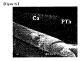
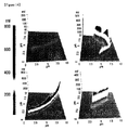
図2Aないし図2Cは、それぞれ本発明の一具現例によるポリチオフェン(PTh)ナノチューブと金属(ニッケル、銅、コバルト)とからなる二重層ナノチューブのSEM写真である。図2Aないし図2Cを参照すれば、ポリチオフェンナノチューブの外部にナノ金属であるニッケル、銅、コバルトがそれぞれ形成された二重層ナノチューブを確認することができる。 2A to 2C are SEM photographs of double-walled nanotubes made of polythiophene (PTh) nanotubes and metals (nickel, copper, cobalt), respectively, according to an embodiment of the present invention. 2A to 2C, double-walled nanotubes in which nickel, copper, and cobalt, which are nanometals, are formed outside the polythiophene nanotubes can be confirmed.
図3は、本発明の一具現例によるPTh−Niからなる二重層ナノチューブの透過電子顕微鏡(Transmission Electron Microscope(TEM)) イメージと回折パターンとである。図3を参照すれば、NiがPThの外部に形成されて直径が200nmであることを確認することができる。図4は、本発明の一具現例によるPTh−Niの高分解能透過電子顕微鏡(HR−TEM)写真である。図4を参照すれば、PThナノチューブ上にNiが蒸着されており、最外郭には酸化によってNiOxが積層されているということを確認することができる。図5は、本発明の一具現例によるPTh−Cuからなる二重層ナノチューブの透過電子顕微鏡(TEM)イメージと高分解能透過電子顕微鏡(HR−TEM)との写真である。製造された二重層ナノチューブ構造は長さが10〜40μmであり、直径がそれぞれ200nm程度であり、発光高分子ナノ物質と金属層との厚さはそれぞれ約10nm程度である。 FIG. 3 is a transmission electron microscope (TEM) image and a diffraction pattern of a double-walled nanotube made of PTh-Ni according to an embodiment of the present invention. Referring to FIG. 3, it can be confirmed that Ni is formed outside PTh and has a diameter of 200 nm. FIG. 4 is a high-resolution transmission electron microscope (HR-TEM) photograph of PTh-Ni according to an embodiment of the present invention. Referring to FIG. 4, it can be confirmed that Ni is vapor-deposited on the PTh nanotubes and NiOx is laminated on the outermost layer by oxidation. FIG. 5 is a photograph of a transmission electron microscope (TEM) image and a high resolution transmission electron microscope (HR-TEM) of a double-walled nanotube made of PTh-Cu according to an embodiment of the present invention. The manufactured double-walled nanotube structure has a length of 10 to 40 μm, a diameter of about 200 nm, and a thickness of each of the light emitting polymer nanomaterial and the metal layer is about 10 nm.
図6A及び図6Bは、それぞれ本発明の一具現例によるPTh−NiとPTh−CuとのX線回折結果である。図6A及び図6Bを参照すれば、X線回折実験を通じてNi及びCuが存在するということを確認することができる。前記図面を参照すれば、最外郭のNiは、Face−centered cubic(FCC)構造を有して格子定数(lattice constant)は約0.2nmであり、銅の場合もFCC構造を有して格子定数は約0.21nmであるということを確認することができる。これは、HR−TEMを用いて測定されたイメージの格子縞の間隔とring patternとを通じて分析した値と一致する。一方、図6Bの右側上部にある図面は、PThナノチューブとPTh−Cu二重層ナノチューブとに対するX線回折実験結果であるが、構造的に大きな変化がないということを確認することができる。 6A and 6B are X-ray diffraction results of PTh—Ni and PTh—Cu, respectively, according to an embodiment of the present invention. Referring to FIGS. 6A and 6B, it can be confirmed that Ni and Cu are present through an X-ray diffraction experiment. Referring to the drawing, the outermost Ni has a face-centered cubic (FCC) structure and a lattice constant of about 0.2 nm, and copper also has an FCC structure and a lattice constant. It can be confirmed that the constant is about 0.21 nm. This agrees with the values analyzed through the lattice pattern spacing and the ring pattern measured using HR-TEM. On the other hand, the drawing in the upper right part of FIG. 6B shows the X-ray diffraction experiment results for the PTh nanotube and the PTh-Cu double-walled nanotube, but it can be confirmed that there is no significant structural change.
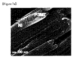
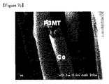
一方、図7Aないし図7Cは、それぞれポリ(3−メチルチオフェン)(P3MT)ナノチューブとニッケル、銅、コバルトからなる二重層ナノチューブとのSEM写真であるが、図7Aないし図7Cを参照すれば、発光高分子ナノチューブの外部でニッケル、銅、コバルトが成長したことを確認することができる。 On the other hand, FIGS. 7A to 7C are SEM photographs of poly (3-methylthiophene) (P3MT) nanotubes and double-walled nanotubes made of nickel, copper, and cobalt. Referring to FIGS. 7A to 7C, It can be confirmed that nickel, copper, and cobalt have grown outside the light-emitting polymer nanotube.
図8は、P3MT−Niの高分解能透過電子顕微鏡写真とEnergy Dispersive Spectroscopy(EDS)結果である。図8を参照すれば、P3MTの外側に結晶構造を有しているナノ単位のニッケル層が均一にコーティングされているということが分かり、EDS結果によれば、内部にはニッケル成分とともにP3MTの硫黄(S)成分が検出されたために内側に発光高分子ナノチューブが形成されており、外側にはナノ単位のニッケル層が均一に形成されているということを確認することができる。また、前記金属−高分子ハイブリッドナノ物質の直径が約200nmであり、発光高分子とニッケルナノチューブとの厚さがそれぞれ約10nmであるということを確認することができる。 FIG. 8 shows high-resolution transmission electron micrographs of P3MT-Ni and energy dispersive spectroscopy (EDS) results. Referring to FIG. 8, it can be seen that a nano-unit nickel layer having a crystal structure is uniformly coated on the outside of P3MT, and according to the EDS results, the P3MT sulfur together with the nickel component is contained inside. It can be confirmed that the light-emitting polymer nanotubes are formed on the inner side because the component (S) is detected, and the nano-unit nickel layer is uniformly formed on the outer side. In addition, it can be confirmed that the diameter of the metal-polymer hybrid nanomaterial is about 200 nm, and the thickness of the light emitting polymer and the nickel nanotube is about 10 nm, respectively.
図9は、それぞれPTh、P3MT、PTh/Ni、P3MT/CuのFouriertransform infrared(FT−IR)結果である。図9を参照すれば、PThとP3MTとがよく形成され、二重構造を有しても主チェーンに大きい構造的な変化がないということを確認することができる。図9に対するピーク(peak)の分析を次の表2及び表3に表わした。 FIG. 9 shows the results of Fourier transform inflation (FT-IR) for PTh, P3MT, PTh / Ni, and P3MT / Cu, respectively. Referring to FIG. 9, it can be confirmed that PTh and P3MT are well formed and that there is no significant structural change in the main chain even if it has a double structure. The peak analysis for FIG. 9 is shown in Tables 2 and 3 below.
図10及び図11は、クロロホルム(CHCl3)溶液内で測定したPTh、P3MTナノチューブのUV/Vis吸収曲線結果である。図10及び図11を参照すれば、UV/Vis吸収曲線を通じて二重層ナノチューブの合成後、スペクトルに構造的な変化があるということを確認することができる。クロロホルム溶液内でそれぞれP3MTは390nm、PThは430nmでp−p*遷移峰が観察されるということを確認した。以後、二重層ナノチューブを形成した後にp−p*遷移峰の大きな変化はないが、560nmと610nmとで新たな吸収が生ずるということを確認することができるが、これは表面プラズモン(surface plasmons、SPs)による影響であると判断される。 10 and 11 are UV / Vis absorption curve results of PTh and P3MT nanotubes measured in a chloroform (CHCl 3 ) solution. Referring to FIGS. 10 and 11, it can be confirmed that there is a structural change in the spectrum after the synthesis of the double-walled nanotube through the UV / Vis absorption curve. In the chloroform solution, it was confirmed that pp * transition peaks were observed at 390 nm for P3MT and 430 nm for PTh, respectively. Thereafter, there is no significant change in the pp * transition peak after the formation of the double-walled nanotube, but it can be confirmed that new absorption occurs at 560 nm and 610 nm, but this can be confirmed by surface plasmons, SPs).
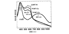
図12は、クロロホルム(CHCl3)溶液内で測定した二重層ナノチューブのPhotoluminescence(PL)結果を表わす。図12を参照すれば、P3MTは約500nm付近で発光をするのに比べて、P3MT−金属は赤色遷移現象を示しつつ、約540nm付近で発光するということを確認することができる。 FIG. 12 represents the photoluminescence (PL) results for double-walled nanotubes measured in chloroform (CHCl 3 ) solution. Referring to FIG. 12, it can be confirmed that P3MT-metal emits light at about 540 nm while exhibiting a red transition phenomenon, compared with P3MT emitting light at about 500 nm.
蛍光強度及びスペクトルの比較
図13は、レーザ共焦点顕微鏡(Laser confocal microscope)を用いて測定した二重層ナノチューブ(PTh−金属)の単一鎖の2次元発光イメージであり、図14は、レーザ共焦点顕微鏡を用いて測定した二重層ナノチューブ(PTh−金属)の単一鎖の発光量の3次元比較イメージである。PTh、PTh−金属の場合に測定された蛍光強度の値を次の表4に表わした。
Comparison of fluorescence intensity and spectrum FIG. 13 is a single-chain two-dimensional emission image of a double-walled nanotube (PTh-metal) measured using a laser confocal microscope, and FIG. It is a three-dimensional comparative image of the light emission amount of a single chain of a double-walled nanotube (PTh-metal) measured using a focus microscope. The fluorescence intensity values measured for PTh and PTh-metal are shown in Table 4 below.
表4を参照すれば、PThのみを使う比較例1と比べて、本発明による実施例1ないし実施例3が、約25で100倍さらに明るいということを確認した。 Referring to Table 4, it was confirmed that Example 1 to Example 3 according to the present invention were about 25 and 100 times brighter than Comparative Example 1 using only PTh.
一方、図15は、レーザ共焦点顕微鏡を用いて測定した二重層ナノチューブ(PTh−金属)の単一鎖のPLスペクトルである。PThは、クロロホルム内で測定された結果より赤色遷移現象を示しつつ、約600nm付近で最大PL強度を示した。しかし、PTh−金属の場合には、約580nm近所でPL強度が急増しながら、630nmと680nmとでPLピークが観察された。最大ピークの強さの差はPThを1であると仮定した時、PTh/Niは70、PTh/uは50、PTh/Coは40で大きな差を見せて二重層の場合、発光強度が大幅に増加するということを確認することができる。 On the other hand, FIG. 15 is a single-chain PL spectrum of a double-walled nanotube (PTh-metal) measured using a laser confocal microscope. PTh showed the maximum PL intensity in the vicinity of about 600 nm while showing a red transition phenomenon from the results measured in chloroform. However, in the case of PTh-metal, the PL peak was observed at 630 nm and 680 nm while the PL intensity rapidly increased in the vicinity of about 580 nm. Assuming that the maximum peak intensity difference is PTh = 1, PTh / Ni is 70, PTh / u is 50, and PTh / Co is 40. Can be confirmed to increase.
図16は、レーザ共焦点顕微鏡を用いて測定した二重層ナノチューブ(P3MT−金属)の単一鎖の発光量の3次元比較イメージである。P3MT、P3MT−金属の場合に測定された蛍光強度の値を次の表5に表わす。 FIG. 16 is a three-dimensional comparison image of single-chain light emission of double-walled nanotubes (P3MT-metal) measured using a laser confocal microscope. The fluorescence intensity values measured for P3MT, P3MT-metal are shown in Table 5 below.
表5を参照すれば、P3MTのみを使う比較例2と比べて、本発明による実施例4ないし実施例6が、約25で167倍さらに明るいということを確認した。 Referring to Table 5, it was confirmed that Examples 4 to 6 according to the present invention were about 25 and 167 times brighter than Comparative Example 2 using only P3MT.
図17は、レーザ共焦点顕微鏡を用いて測定した二重層ナノチューブ(P3MT−金属)の単一鎖のPLスペクトルである。P3MTは、クロロホルム内で測定された結果より赤色遷移現象を示しつつ、約580nm付近で最大PL強度を示した。しかし、P3MT−金属の場合には、約580nm近所でPL強度が急増しながら、630nmと680nmとでPLピークが観察された。最大ピークの強さの差はPThを1であると仮定した時、P3MT/Cuは100、P3MT/Niは50、P3MT/Coは20で大きな差を見せて二重層の場合、発光強度が大幅に増加するということを確認することができる。 FIG. 17 is a single-chain PL spectrum of a double-walled nanotube (P3MT-metal) measured using a laser confocal microscope. P3MT showed the maximum PL intensity around about 580 nm while showing a red transition phenomenon from the results measured in chloroform. However, in the case of P3MT-metal, the PL peak was observed at 630 nm and 680 nm while the PL intensity rapidly increased in the vicinity of about 580 nm. Assuming that the maximum peak intensity difference is 1 for PTh, P3MT / Cu is 100, P3MT / Ni is 50, P3MT / Co is 20, showing a large difference. Can be confirmed to increase.
前記の結果から固体状態で相対的に光度が小さな発光高分子ナノ物質をナノ単位の金属層で取り囲みながら、二重層ナノチューブを形成する場合に、光度が大きく増加する新たな現象を発見した。また、P3MTを成長させた後、Niを時間を調節して部分成長させた後に観察した単一鎖の結果でニッケルが取り囲まれた部分を境界で発光強度が急激に変わるということを確認した。すなわち、これを通じて金属の構造が、発光高分子ナノ物質の発光現象を向上させることに寄与するということを確認することができる。 From the above results, we discovered a new phenomenon in which the luminous intensity is greatly increased when a double-walled nanotube is formed while surrounding a light-emitting polymer nanomaterial having a relatively small luminous intensity in a solid state with a nano-unit metal layer. In addition, after growing P3MT, it was confirmed that the emission intensity abruptly changed at the boundary of the portion surrounded by nickel as a result of the single chain observed after partial growth of Ni by adjusting the time. That is, it can be confirmed that the metal structure contributes to improving the light-emitting phenomenon of the light-emitting polymer nanomaterial.
図18は、二重層ナノチューブの発光現象分析のために測定したニッケルと銅ナノ線とのUV/Vis吸収曲線結果を表わす。新たな構造を確認するために、発光高分子ナノ物質のなしにニッケルと銅ナノワイヤとを成長してUV/Vis吸収曲線を測定したものである。図18を参照すれば、二重層ナノチューブで見える新たな構造が、ナノ金属で起因したことであるという事実を確認することができる。二重層ナノチューブの発光現象分析のために測定したPL効率結果を次の表6に表わした。 FIG. 18 shows the UV / Vis absorption curve results of nickel and copper nanowires measured for the analysis of the light emission phenomenon of double-walled nanotubes. In order to confirm a new structure, a UV / Vis absorption curve was measured by growing nickel and copper nanowires without using a light emitting polymer nanomaterial. Referring to FIG. 18, it can be confirmed that the new structure seen in the double-walled nanotube is due to the nanometal. The PL efficiency results measured for the analysis of the light emission phenomenon of the double-walled nanotube are shown in Table 6 below.
表6を参照すれば、PL効率測定を通じて比較例1、2に比べて実施例1ないし6が、約2〜2.5倍程度PL効率が増加するということを確認した。前記の結果を分析して見れば、二重層ナノチューブが優れた発光現象を示す理由は、表面プラズモンによるエキシトン形成の増加が最も大きな要因であると見られる。したがって、発光高分子ナノ物質、及び前記発光高分子ナノ物質のバンドギャップと表面プラズモンバンドギャップとが一致する金属を使うことで、発光効率を大幅に増加させうるということが分かる。 Referring to Table 6, it was confirmed that the PL efficiency increased by about 2 to 2.5 times in Examples 1 to 6 as compared with Comparative Examples 1 and 2 through PL efficiency measurement. From the analysis of the above results, the reason why the double-walled nanotubes exhibit an excellent light emission phenomenon seems to be the largest factor in the increase in exciton formation by surface plasmons. Therefore, it can be seen that the luminous efficiency can be significantly increased by using the light emitting polymer nanomaterial and the metal having the same band gap as the surface plasmon bandgap of the light emitting polymer nanomaterial.
(実験例2)
UV/Vis吸収曲線を通じるドーピング状態の確認
電気化学方法を用いて発光高分子P3MTナノチューブを合成し、サイクリックボルタンメトリーを用いてドーピング状態を調節した後、HFで多孔性アルミナテンプレートを除去した後にクロロホルムに均一に分散させてUV/Vis吸収曲線スペクトルを測定して発光高分子ナノチューブのドーピング状態の変化を確認した。図19は、クロロホルムに発光高分子P3MTナノチューブを均一に分散させた後、測定したUV/Vis吸収曲線スペクトルである。図19を参照すれば、吸収遷移に該当する最大ピークは390nmであり、ドーピングが進行することによってバイポーラロン吸収に該当する800nmの吸収の強さが大きくなることを確認することができた。吸収遷移の強さを1であるとした時、バイポーラロンの強さを0.67、0.52、0.25、0.04で調節した。
(Experimental example 2)
Confirmation of doping state through UV / Vis absorption curve After synthesizing luminescent polymer P3MT nanotubes using electrochemical method, adjusting doping state using cyclic voltammetry, removing porous alumina template with HF, chloroform The UV / Vis absorption curve spectrum was measured by uniformly dispersing the light-emitting polymer nanotubes and the change in the doping state of the light-emitting polymer nanotubes was confirmed. FIG. 19 is a UV / Vis absorption curve spectrum measured after uniformly dispersing light-emitting polymer P3MT nanotubes in chloroform. Referring to FIG. 19, the maximum peak corresponding to the absorption transition is 390 nm, and it can be confirmed that the intensity of absorption at 800 nm corresponding to bipolaron absorption increases with the progress of doping. Assuming that the intensity of the absorption transition is 1, the intensity of the bipolaron was adjusted to 0.67, 0.52, 0.25, and 0.04.
(実験例3)
共焦点顕微鏡を利用した発光強度の比較
図20は、共焦点顕微鏡を利用したバイポーラロンのドーピング状態が、0.04と0.67とであるP3MTナノチューブと、これらにナノ単位のニッケル層が取り囲まれた異種二重壁P3MTナノチューブの光発光強度を比べるための単一鎖の2次元光発光イメージである。単純なP3MTナノチューブの場合には、ドーピング状態が0.67である場合、発光強度が最も弱いながら0.04でドーピング状態が減少するにつれて発光強度が増加する現象を観察した。しかし、ナノ単位のニッケル層が取り囲まれたP3MT/Niナノチューブの場合には、ドーピング状態が0.04である場合より0.67である場合、発光強度が巨大に増加する現象を観察することができた。さらに定量的な比較のために、図21には、前記発光強度をボルト(V)単位で測定して3次元発光イメージで比べ、図22には、PLスペクトルの強さを比べた。前記図面を参照すれば、ドーピング状態が減少するほど発光強度が増加し、最大発光ピークが赤色遷移するということを確認することができる。すなわち、測定された発光イメージの強さは、P3MTナノチューブのドーピング程度が0.04である場合が約40〜44mVであり、ドーピング程度が0.67である場合が約58mVで5〜11倍程度発光強度が差が生ずるということを確認した。図22の単一鎖の光発光スペクトルの結果でドーピング状態が最も高い場合(バイポーラロン吸収の強さが0.67である場合)のPL強度を1で規格化した時、ドーピング状態が最も低い場合(バイポーラロン吸収の強さが0.04である場合)は、PL強度が14で発光強度が増加する現象を観察することができる。また、ドーピング状態が減少するにつれて最大峰の位置が560nmの緑色発光で約580nm近所で光発光強度が急増しながら、640nmと685nmとで光発光最大ピークで赤色遷移現象を示しつつ、赤色の発光が観察される。
(Experimental example 3)
Comparison of emission intensity using confocal microscope FIG. 20 shows P3MT nanotubes having bipolaron doping states of 0.04 and 0.67 using a confocal microscope, and a nano-unit nickel layer surrounded by them. 2 is a single-chain two-dimensional light emission image for comparing the light emission intensities of different kinds of double-walled P3MT nanotubes. In the case of a simple P3MT nanotube, when the doping state was 0.67, the phenomenon was observed in which the emission intensity increased as the doping state decreased at 0.04 although the emission intensity was the weakest. However, in the case of P3MT / Ni nanotubes surrounded by a nano-unit nickel layer, it is possible to observe a phenomenon in which the emission intensity increases enormously when the doping state is 0.67 than when the doping state is 0.04. did it. For further quantitative comparison, FIG. 21 compares the emission intensity measured in volts (V) with a three-dimensional emission image, and FIG. 22 compares the PL spectrum intensity. Referring to the drawing, it can be confirmed that the emission intensity increases as the doping state decreases and the maximum emission peak undergoes a red transition. That is, the intensity of the measured light emission image is about 40 to 44 mV when the doping degree of the P3MT nanotube is 0.04, and about 5 to 11 times at about 58 mV when the doping degree is 0.67. It was confirmed that there was a difference in emission intensity. When the PL intensity in the case where the doping state is the highest (when the intensity of bipolaron absorption is 0.67) is normalized by 1 as a result of the single-chain photoluminescence spectrum of FIG. 22, the doping state is the lowest. In the case (when the intensity of bipolaron absorption is 0.04), the phenomenon that the PL intensity is 14 and the emission intensity increases can be observed. Further, as the doping state decreases, the maximum peak position is green emission at 560 nm, and the light emission intensity rapidly increases in the vicinity of about 580 nm, while the red light emission phenomenon is exhibited at the maximum light emission peak at 640 nm and 685 nm, while the red emission Is observed.
一方、図23と図24とには、レーザ共焦点顕微鏡を用いてドーピング状態の変化によるP3MT/Niハイブリッドナノチューブの発光強度を比べた。本図面を参照すれば、バイポーラロンの強さの程度と関係なく約580nm近所で光発光強度が急増しながら、630nmと680nmとで光発光の峰が観察された。ナノ単位のニッケル層を取り囲んだ後、バイポーラロン状態がほとんどない場合(ドーピング状態0.04)は、単純なP3MTナノチューブの場合より約10倍の光発光強度の増加が観察されたが、バイポーラロンの強さが最も強い場合(ドーピング状態0.67)には、約350倍の光発光強度の増加が観察された。3次元発光イメージでは、ドーピング程度が0.04である場合が約1.2〜1.6Vであり、ドーピング程度が0.67である場合が約3.1〜3.8Vでドーピング状態が増加するほど発光強度が増加しているということを確認することができる。これは、既述したように、表面プラズモン共鳴によるエネルギー伝達及び電子伝達によってエキシトンの数が増加するためである。 On the other hand, in FIG. 23 and FIG. 24, the light emission intensity of the P3MT / Ni hybrid nanotube due to the change of the doping state was compared using a laser confocal microscope. Referring to this drawing, light emission peaks were observed at 630 nm and 680 nm, while the light emission intensity increased rapidly in the vicinity of about 580 nm regardless of the degree of bipolaron intensity. In the absence of a bipolaron state after doping the nano-unit nickel layer (doping state 0.04), an approximately 10-fold increase in light emission intensity was observed compared to a simple P3MT nanotube. When the intensity of light was the strongest (doping state 0.67), an increase in light emission intensity of about 350 times was observed. In the three-dimensional light emission image, the doping level is about 1.2 to 1.6 V when the doping degree is 0.04, and the doping state is about 3.1 to 3.8 V when the doping degree is 0.67. It can be confirmed that the emission intensity increases as the time increases. As described above, this is because the number of excitons increases due to energy transfer and electron transfer by surface plasmon resonance.
下記表7は、ドーピング程度によるP3MTナノチューブの発光強度とP3MT/Niハイブリッドナノチューブの発光強度とを3次元PLイメージの強さで比べたデータであり、表8は、PLスペクトルの強さで比べたデータである。 Table 7 below shows data comparing the emission intensity of the P3MT nanotubes according to the doping level and the emission intensity of the P3MT / Ni hybrid nanotubes by the intensity of the three-dimensional PL image, and Table 8 comparing the intensity of the PL spectrum. It is data.
(実験例4)
巨大発光効率の増加分析結果
発光高分子ナノチューブのドーピング状態の変化による発光効率の変化とナノ規模の金属のコーティングされた異種二重壁P3MTナノチューブの巨大発光効率の増加とを分析するために、UV/Vis吸収曲線、及び光発光の量子効率を測定した。図25は、バイポーラロン状態で電荷伝達現象の証拠を確認するためのUV/Vis吸収曲線である。小文字a、b、c及びdは、それぞれP3MT(0.04)、P3MT(0.25)、P3MT(0.52)及びP3MT(0.67)を表わし、大文字A、B、C及びDは、それぞれP3MT(0.04)/Ni、P3MT(0.25)/Ni、P3MT(0.52)/Ni及びP3MT(0.67)/Niを表わす。
(Experimental example 4)
Results of Analysis of Increased Giant Luminous Efficiency In order to analyze the change in luminous efficiency due to the change of doping state of luminescent polymer nanotubes and the increased luminous efficiency of heterogeneous double-walled P3MT nanotubes coated with nanoscale metals, The / Vis absorption curve and the quantum efficiency of light emission were measured. FIG. 25 is a UV / Vis absorption curve for confirming the evidence of the charge transfer phenomenon in the bipolaron state. Lowercase letters a, b, c and d represent P3MT (0.04), P3MT (0.25), P3MT (0.52) and P3MT (0.67), respectively, and uppercase letters A, B, C and D are P3MT (0.04) / Ni, P3MT (0.25) / Ni, P3MT (0.52) / Ni and P3MT (0.67) / Ni, respectively.
UV/Vis吸収曲線を通じてクロロホルム溶液内でP3MTナノチューブは、390nmでp−p*遷移峰が観察される。P3MT/Niナノチューブを形成した後にp−p*遷移峰の大きな変化はないが、表面プラズモン(SPs)による影響であると判断される563nmと615nmとで新たな吸収ピークが観察され、その強さはドーピング程度が0.04から0.67にバイポーラロン状態が強いほど増加するということを確認することができる。これは、ナノ単位のニッケル層で取り囲まれたハイブリッドP3MTナノチューブでバイポーラロン状態を通じる電荷伝達現象とエネルギー伝達現象とが起きるためである。図26は、バイポーラロン状態による発光効率を分析するためのP3MTナノチューブとハイブリッドP3MT/Niナノチューブとの光発光の量子効率結果である。クロロホルム溶液内で測定した光発光の量子効率でバイポーラロン状態が0.04から0.67に増加するほどP3MTナノチューブは、0.102から0.029に減少する傾向を見せているが、ハイブリッドP3MT/Niナノチューブの場合は、反対に0.129から0.221に増加する現象を示しつつ、バイポーラロン状態が最も強い場合に、大きな光発光の量子効率が観察される。すなわち、ドーピング状態が0.04である場合は、光発光の量子効率が0.102から0.129に約1.3倍増加し、ドーピング状態が0.67である場合は、光発光の量子効率が0.029から0.221に7.6倍に増加するということを確認することができる。 A pp * transition peak is observed at 390 nm for P3MT nanotubes in chloroform solution through a UV / Vis absorption curve. Although there is no significant change in the pp * transition peak after the formation of the P3MT / Ni nanotube, new absorption peaks are observed at 563 nm and 615 nm, which are judged to be the influence of surface plasmons (SPs), and their strengths It can be confirmed that the doping level increases from 0.04 to 0.67 as the bipolaron state increases. This is because the charge transfer phenomenon and the energy transfer phenomenon through the bipolaron state occur in the hybrid P3MT nanotube surrounded by the nano-unit nickel layer. FIG. 26 is a quantum efficiency result of light emission of P3MT nanotubes and hybrid P3MT / Ni nanotubes for analyzing light emission efficiency in the bipolaron state. P3MT nanotubes tend to decrease from 0.102 to 0.029 as the bipolaron state increases from 0.04 to 0.67 due to the quantum efficiency of photoluminescence measured in chloroform solution, but the hybrid P3MT In the case of / Ni nanotubes, on the contrary, a large quantum efficiency of light emission is observed when the bipolaron state is strongest while showing a phenomenon increasing from 0.129 to 0.221. That is, when the doping state is 0.04, the quantum efficiency of light emission increases by about 1.3 times from 0.102 to 0.129, and when the doping state is 0.67, the quantum efficiency of light emission It can be seen that the efficiency increases 7.6 times from 0.029 to 0.221.
(実験例5)
巨大発光効率の増加解析のためのエネルギーバンド図式図
図27は、ハイブリッドP3MT/Niナノチューブの巨大発光効率の増加を説明するためのエネルギーバンド図式図を表わす。前記の結果を分析して見れば、高分子−金属ハイブリッドナノ物質が優れた発光現象を示す理由は、表面プラズモン共鳴状態でエネルギー伝達と電荷伝達現象とによるエキシトン増加が最も大きな要因であると見られる。図27の表面プラズモン共鳴による巨大発光効率の増加は、次のように説明することができる。非ドーピング状態で約2.0eVを表わすP3MTの例を有して記述する。ナノ規模のニッケルによる表面プラズモンエネルギーは、約2.03〜2.19eV(563〜615nm)であり、発光高分子P3MTのバンドギャップはドーピング状態によって2.0〜2.3eVまで調節が可能である。ニッケルとP3MTとがナノ規模の接合を形成すれば、金属と半導体との接合によってフェルミエネルギー準位が合わせられ、ニッケルの表面プラズモンエネルギーがP3MTの伝導準位より高位置に存在する。すなわち、ドーピング状態によってバンドギャップ内に形成されるバイポーラロンを通じてニッケルで電子伝達が可能となり、金属の表面プラズモン共鳴エネルギー準位を通じてP3MTとエネルギー伝達とが可能となる。それによって、より多くのエキシトンが形成され、発光高分子であるP3MTの巨大発光効率の増加現象を起こしうる。
(Experimental example 5)
FIG. 27 is an energy band diagram for explaining the increase in the giant luminous efficiency of the hybrid P3MT / Ni nanotube. Analyzing the above results, the reason why polymer-metal hybrid nanomaterials exhibit an excellent light emission phenomenon is that the increase in excitons due to energy transfer and charge transfer phenomena in the surface plasmon resonance state is the largest factor. It is done. The increase in the giant light emission efficiency due to the surface plasmon resonance of FIG. 27 can be explained as follows. Described with an example of P3MT representing approximately 2.0 eV in the undoped state. The surface plasmon energy of nanoscale nickel is about 2.03 to 2.19 eV (563 to 615 nm), and the band gap of the light emitting polymer P3MT can be adjusted from 2.0 to 2.3 eV depending on the doping state. . If nickel and P3MT form a nano-scale junction, the Fermi energy level is matched by the junction between the metal and the semiconductor, and the surface plasmon energy of nickel is higher than the conduction level of P3MT. That is, electrons can be transferred with nickel through bipolarons formed in the band gap depending on the doping state, and energy transfer with P3MT can be performed through the surface plasmon resonance energy level of the metal. As a result, more excitons are formed, which may cause a phenomenon that the giant light emission efficiency of P3MT, which is a light emitting polymer, increases.
Claims (7)
(b)H2O、アセトニトリル及びN−メチルピロリジノンからなる群から選択された何れか一つ以上の極性溶媒と、チオフェン、3−メチルチオフェン、3−アルキルチオフェン、3,4−エチレンジオキシチオフェン、アニリン、1,4−フェニレンビニレン、フェニレン及びその誘導体からなる群から選択された一つ以上の単量体と、ドーパントを含む混合液を撹拌して重合溶液を形成し、これを前記多孔性テンプレートのナノ気孔内で重合してπ共役構造の発光高分子を含むナノチューブまたはナノワイヤとを形成する段階と、
(c)前記ナノチューブまたはナノワイヤを有機溶液に浸漬させてサイクリックボルタンメトリーを用いてドーピング及び非ドーピングさせる段階と、
(d)前記ナノチューブの内外側または前記ナノワイヤの外側に金属を電気化学的に蒸着して金属層を形成する段階と、
(e)前記多孔性テンプレートを除去する段階と、を含んでおり、
前記(d)段階の金属は、銅(Cu)、コバルト(Co)、鉄(Fe)、亜鉛(Zn)、チタン(Ti)、クロム(Cr)、銀(Ag)、金(Au)、白金(Pt)、アルミニウム(Al)、及びこれらの複合体からなる群から選択された何れか一つ以上であることを特徴とする光電子素子用の金属−高分子ハイブリッドナノ物質の光学特性の調節方法。 (A) attaching a metal used as an electrode to a porous template in which nano-sized pores are formed;
(B) any one or more polar solvents selected from the group consisting of H 2 O, acetonitrile and N-methylpyrrolidinone, thiophene, 3-methylthiophene, 3-alkylthiophene, 3,4-ethylenedioxythiophene , A mixed solution containing one or more monomers selected from the group consisting of aniline, 1,4-phenylene vinylene, phenylene and derivatives thereof, and a dopant to form a polymerization solution, which is formed into the porous material. Polymerizing within the nanopores of the template to form nanotubes or nanowires comprising a luminescent polymer of π-conjugated structure;
(C) immersing the nanotube or nanowire in an organic solution and doping and undoping using cyclic voltammetry;
(D) forming a metal layer by electrochemically depositing metal on the inside or outside of the nanotube or outside the nanowire;
(E) removing the porous template;
The metals in the step (d) are copper (Cu), cobalt (Co), iron (Fe), zinc (Zn), titanium (Ti), chromium (Cr), silver (Ag), gold (Au), platinum. (Pt), aluminum (Al), and any one or more selected from the group consisting of these composites, and a method for adjusting optical properties of metal-polymer hybrid nanomaterials for optoelectronic devices .
アセトニトリルとドーパントとの混合溶液であることを特徴とする請求項1に記載の光電子素子用の金属−高分子ハイブリッドナノ物質の光学特性の調節方法。 The organic solution in step (c) is
The method for adjusting optical properties of metal-polymer hybrid nanomaterials for optoelectronic devices according to claim 1 , wherein the method is a mixed solution of acetonitrile and a dopant.
カンポスルホン酸、ベンゼンスルホン酸、p−ドデシルベンゼンスルホン酸、テトラブチルアンモニウムヘキサフルオロホスフェート、テトラブチルアンモニウムテトラフルオロボレート、1−ブチル−3−メチルイミダゾリウムヘキサフルオロホスフェート、ナフタレンスルホン酸、ポリ(4−スチレンスルホン酸)、HCl及びp−トルエンスルホン酸からなる群から選択された何れか一つ以上であることを特徴とする請求項1または2に記載の光電子素子用の金属−高分子ハイブリッドナノ物質の光学特性の調節方法。 The dopant is
Camposulfonic acid, benzenesulfonic acid, p-dodecylbenzenesulfonic acid, tetrabutylammonium hexafluorophosphate, tetrabutylammonium tetrafluoroborate, 1-butyl-3-methylimidazolium hexafluorophosphate, naphthalenesulfonic acid, poly (4- 3. The metal-polymer hybrid nanomaterial for optoelectronic devices according to claim 1 , wherein the metal-polymer hybrid nanomaterial for optoelectronic devices is one or more selected from the group consisting of styrene sulfonic acid), HCl, and p-toluenesulfonic acid. Method of adjusting the optical properties of the screen.
多孔性テンプレートをHFまたはNaOH水溶液に浸漬させて除去して、金属−高分子ハイブリッドナノ物質を得ることを特徴とする請求項1に記載の光電子素子用の金属−高分子ハイブリッドナノ物質の光学特性の調節方法。 In step (e),
2. The optical property of the metal-polymer hybrid nanomaterial for optoelectronic devices according to claim 1 , wherein the metal-polymer hybrid nanomaterial is obtained by immersing and removing the porous template in an aqueous solution of HF or NaOH. Adjustment method.
ドーパントによってナノチューブまたはナノワイヤのバンドギャップの間にバイポーラロンバンドが形成され、前記バイポーラロンバンドに存在する電子が表面プラズモン共鳴によって金属層のフェルミ準位に移動する電子伝達によることを特徴とする請求項1に記載の光電子素子用の金属−高分子ハイブリッドナノ物質の光学特性の調節方法。 The adjustment of the optical property is
Bipolaron band between the band gap of the nanotubes or nanowires are formed by a dopant, claims electrons present in the bipolaron band is characterized in that by electron transfer to move the Fermi level of the metal layer by surface plasmon resonance 2. The method for adjusting optical properties of metal-polymer hybrid nanomaterials for optoelectronic devices according to 1 .
Applications Claiming Priority (3)
| Application Number | Priority Date | Filing Date | Title |
|---|---|---|---|
| KR10-2007-0093340 | 2007-09-13 | ||
| KR1020070093340A KR100955881B1 (en) | 2007-09-13 | 2007-09-13 | Method for controlling luminescent characteristics of double walled nanotubes |
| PCT/KR2008/005460 WO2009035308A2 (en) | 2007-09-13 | 2008-09-16 | Metal-polymer hybrid nanomaterials, method for preparing the same method for controlling optical property of the same and optoelectronic device using the same |
Publications (2)
| Publication Number | Publication Date |
|---|---|
| JP2010508387A JP2010508387A (en) | 2010-03-18 |
| JP5428038B2 true JP5428038B2 (en) | 2014-02-26 |
Family
ID=40452723
Family Applications (1)
| Application Number | Title | Priority Date | Filing Date |
|---|---|---|---|
| JP2009534518A Expired - Fee Related JP5428038B2 (en) | 2007-09-13 | 2008-09-16 | Metal-polymer hybrid nanomaterial, method for producing the same, method for adjusting optical properties of metal-polymer hybrid nanomaterial, and optoelectronic device using the same |
Country Status (5)
| Country | Link |
|---|---|
| US (1) | US20100075145A1 (en) |
| EP (1) | EP2089313A4 (en) |
| JP (1) | JP5428038B2 (en) |
| KR (1) | KR100955881B1 (en) |
| WO (1) | WO2009035308A2 (en) |
Families Citing this family (21)
| Publication number | Priority date | Publication date | Assignee | Title |
|---|---|---|---|---|
| JP2010031168A (en) * | 2008-07-30 | 2010-02-12 | Kinki Univ | Polymer nanotube bonding nanoparticles and method of producing the same |
| WO2010111741A1 (en) * | 2009-03-31 | 2010-10-07 | Curtin University Of Technology | Nanomaterials and methods of preparation therefor |
| FR2952928A1 (en) * | 2009-11-20 | 2011-05-27 | Centre Nat Rech Scient | Method for realization of organized network of nano-objects on substrate, involves depositing material contained in pores of membrane on substrate to form organized network of nano-objects on substrate |
| CN102214517B (en) * | 2010-04-07 | 2012-12-19 | 财团法人交大思源基金会 | Method for manufacturing large-area solar cell |
| CN102071468B (en) * | 2011-02-24 | 2012-10-24 | 南京师范大学 | Independent polymer nanotube, and preparation method and application thereof |
| CN102337571B (en) * | 2011-11-03 | 2014-01-08 | 厦门建霖工业有限公司 | Method for electroplating plastic base material |
| CN102522210B (en) * | 2011-11-16 | 2014-11-19 | 东南大学 | Polypyrrole nano-tube embedded nano-pore array material as well as preparation method and energy storage application thereof |
| KR101357722B1 (en) * | 2012-03-05 | 2014-02-05 | 연세대학교 산학협력단 | Metal nanoparticles-fluorescent material having enhanced fluorescene and method for preparing the same |
| EP2911159A4 (en) * | 2012-10-24 | 2016-04-06 | Nat Inst For Materials Science | Adhesive body between conductive polymer-metal complex and substrate and method for forming adhesive body, conductive polymer-metal complex dispersion liquid, method for manufacturing and applying same, and method for filling hole using conductive material |
| WO2014123860A2 (en) | 2013-02-06 | 2014-08-14 | President And Fellows Of Harvard College | Anisotropic deposition in nanoscale wires |
| US10435817B2 (en) | 2014-05-07 | 2019-10-08 | President And Fellows Of Harvard College | Controlled growth of nanoscale wires |
| DE102015101809B4 (en) * | 2015-02-09 | 2020-05-28 | Arne Hensel | Lighting device |
| DE102015103895A1 (en) * | 2015-03-17 | 2016-09-22 | Osram Oled Gmbh | Method for producing an organic component |
| CN104892935B (en) * | 2015-05-21 | 2017-03-01 | 安徽大学 | A kind of method of synthesized polyaniline nanotube |
| KR101826413B1 (en) | 2016-03-24 | 2018-02-06 | 포항공과대학교 산학협력단 | Three dimensional hybrid nanostructures based materials for efficient photochemical or photoelectrochemical reaction and manufacturing method thereof |
| KR102345917B1 (en) * | 2020-04-27 | 2021-12-30 | 국민대학교산학협력단 | Micro-nano-fin light-emitting diodes and method for manufacturing thereof |
| US20230223492A1 (en) * | 2020-04-27 | 2023-07-13 | Kookmin University Industry Academy Cooperation Foundation | Micro-nanopin led element and method for producing same |
| KR102332349B1 (en) * | 2020-04-28 | 2021-11-26 | 국민대학교산학협력단 | Micro-nano-fin light-emitting diodes and method for manufacturing thereof |
| KR102332350B1 (en) * | 2020-05-25 | 2021-11-26 | 국민대학교산학협력단 | Micro-nano-fin light-emitting diodes electrode assembly and method for manufacturing thereof |
| CN111717887A (en) * | 2020-07-01 | 2020-09-29 | 福建师范大学 | Micron-sized fixed-point positioning nano material transfer method |
| CN117186462B (en) * | 2023-11-08 | 2024-02-02 | 华中科技大学 | Polymer-based flexible film with oriented bridging structure, preparation and application |
Family Cites Families (11)
| Publication number | Priority date | Publication date | Assignee | Title |
|---|---|---|---|---|
| US4541905A (en) * | 1983-12-13 | 1985-09-17 | The Ohio State University Research Foundation | Electrodes for use in electrocatalytic processes |
| TW541853B (en) * | 2000-11-10 | 2003-07-11 | Sumitomo Chemical Co | Polymeric fluorescent substance and polymer light-emitting device using the same |
| US7204895B2 (en) * | 2002-04-15 | 2007-04-17 | Lg Chem, Ltd. | Electropolymerization method for preparing nano-tube type conducting polymer using porous template, method for preparing electrochromic device, and electrochromic device prepared therefrom |
| KR100495625B1 (en) | 2002-04-23 | 2005-06-16 | 대주전자재료 주식회사 | Conjugated polymer-inorganic particulate composite composition for luminescent layer of organic electroluminescence device |
| KR100484317B1 (en) * | 2002-07-29 | 2005-04-20 | 학교법인고려중앙학원 | π-conjugated polymer nano-tube, nano-wier and method for preparing the same |
| KR100537966B1 (en) | 2003-04-30 | 2005-12-21 | 한국과학기술연구원 | Polymer electroluminescent device using emitting layer of nanocomposites |
| JP4528927B2 (en) * | 2003-09-04 | 2010-08-25 | 独立行政法人産業技術総合研究所 | Composite fine particle production method, composite fine particle production apparatus, and composite fine particle |
| KR100672872B1 (en) * | 2005-10-28 | 2007-01-24 | 한국과학기술연구원 | Fabrication method of three dimensional nanostructure |
| KR100736515B1 (en) | 2005-12-01 | 2007-07-06 | 삼성전자주식회사 | Method for Producing Nanowire Using Porous Template and Nanowire Structure |
| US20100068461A1 (en) * | 2006-06-30 | 2010-03-18 | University Of Wollongong | Nanostructured composites |
| KR100858931B1 (en) * | 2007-05-03 | 2008-09-17 | 고려대학교 산학협력단 | Doble walled nanotubes and doble walled nanowires |
-
2007
- 2007-09-13 KR KR1020070093340A patent/KR100955881B1/en active IP Right Grant
-
2008
- 2008-09-16 WO PCT/KR2008/005460 patent/WO2009035308A2/en active Application Filing
- 2008-09-16 EP EP08830475A patent/EP2089313A4/en not_active Withdrawn
- 2008-09-16 US US12/312,264 patent/US20100075145A1/en not_active Abandoned
- 2008-09-16 JP JP2009534518A patent/JP5428038B2/en not_active Expired - Fee Related
Also Published As
| Publication number | Publication date |
|---|---|
| WO2009035308A2 (en) | 2009-03-19 |
| KR100955881B1 (en) | 2010-05-06 |
| WO2009035308A3 (en) | 2009-07-02 |
| JP2010508387A (en) | 2010-03-18 |
| EP2089313A2 (en) | 2009-08-19 |
| KR20090028068A (en) | 2009-03-18 |
| EP2089313A4 (en) | 2011-03-09 |
| US20100075145A1 (en) | 2010-03-25 |
Similar Documents
| Publication | Publication Date | Title |
|---|---|---|
| JP5428038B2 (en) | Metal-polymer hybrid nanomaterial, method for producing the same, method for adjusting optical properties of metal-polymer hybrid nanomaterial, and optoelectronic device using the same | |
| KR100858931B1 (en) | Doble walled nanotubes and doble walled nanowires | |
| Sumdani et al. | Recent advancements in synthesis, properties, and applications of conductive polymers for electrochemical energy storage devices: A review | |
| KR101746551B1 (en) | Carbon nanotube composite structures and methods of manufacturing the same | |
| Jin et al. | Synthesis of freestanding PEDOT: PSS/PVA@ Ag NPs nanofiber film for high-performance flexible thermoelectric generator | |
| Reddy et al. | Synthesis of MWCNTs‐core/thiophene polymer‐sheath composite nanocables by a cationic surfactant‐assisted chemical oxidative polymerization and their structural properties | |
| Park et al. | Hybrid nanostructures using π-conjugated polymers and nanoscale metals: Synthesis, characteristics, and optoelectronic applications | |
| Wang et al. | Viologen-bridged polyaniline based multifunctional heterofilms for all-solid-state supercapacitors and memory devices | |
| KR20080073019A (en) | Nano or micro sized organic-inorganic composite device and method of producing thereof | |
| Rohom et al. | Enhancement of optical absorption by incorporation of plasmonic nanoparticles in PANI films | |
| KR101077968B1 (en) | Metal-Polymer hybrid nanomaterials, method for preparing the same and optoelectronic device using the same | |
| Rayar et al. | Organic conjugated polymers and their nanostructured composites: Synthesis methodologies and electrochemical applications | |
| Hosseinzade et al. | Electrochemical deposition of NiO bunsenite nanostructures with different morphologies as the hole transport layer in polymer solar cells | |
| Park et al. | Significantly Enhanced Photoluminescence of Doped Polymer‐Metal Hybrid Nanotubes | |
| KR101147221B1 (en) | Polythiophene based polymer nano material and method for controlling the properties of photoluminesence and conductivity of the same | |
| Singh | Composites based on conducting polymers and carbon nanotubes for supercapacitors | |
| KR100484317B1 (en) | π-conjugated polymer nano-tube, nano-wier and method for preparing the same | |
| Sehgal et al. | Structural, morphological, optical, and electrical transport studies of poly (3-methoxythiophene)/NiO hybrid nanocomposites | |
| CN1598971A (en) | Conducting polymer carbon nanotube nano cable and preparation method thereof | |
| Bhattacharya | Conducting-polymer-based supercapacitors | |
| Kukhta | Organic-inorganic nanocomposites and their applications | |
| KR20090085788A (en) | Poly (3,4-ethylenedioxythiophene)(pedot) nanowires for organic photoelectric device, method for cotrolling the properties of photoluminescence | |
| Jose et al. | In situ chemical oxidative polymerisation for ordered conducting polythiophene nanostructures in presence of dioctyl sodium sulfosuccinate | |
| KR101010856B1 (en) | Optoelectronic devices and method of manufacturing of the same | |
| KR20110124502A (en) | Method of modifying light-emitting polymer through focused e-beam, method of manufacturing nano barcode through focused e-beam and nano barcode manufactured by the method |
Legal Events
| Date | Code | Title | Description |
|---|---|---|---|
| A131 | Notification of reasons for refusal |
Free format text: JAPANESE INTERMEDIATE CODE: A131 Effective date: 20120529 |
|
| A601 | Written request for extension of time |
Free format text: JAPANESE INTERMEDIATE CODE: A601 Effective date: 20120824 |
|
| A602 | Written permission of extension of time |
Free format text: JAPANESE INTERMEDIATE CODE: A602 Effective date: 20120831 |
|
| A601 | Written request for extension of time |
Free format text: JAPANESE INTERMEDIATE CODE: A601 Effective date: 20120921 |
|
| A602 | Written permission of extension of time |
Free format text: JAPANESE INTERMEDIATE CODE: A602 Effective date: 20120928 |
|
| A521 | Request for written amendment filed |
Free format text: JAPANESE INTERMEDIATE CODE: A523 Effective date: 20121029 |
|
| A131 | Notification of reasons for refusal |
Free format text: JAPANESE INTERMEDIATE CODE: A131 Effective date: 20130402 |
|
| A521 | Request for written amendment filed |
Free format text: JAPANESE INTERMEDIATE CODE: A523 Effective date: 20130627 |
|
| TRDD | Decision of grant or rejection written | ||
| A01 | Written decision to grant a patent or to grant a registration (utility model) |
Free format text: JAPANESE INTERMEDIATE CODE: A01 Effective date: 20131015 |
|
| A61 | First payment of annual fees (during grant procedure) |
Free format text: JAPANESE INTERMEDIATE CODE: A61 Effective date: 20131108 |
|
| R150 | Certificate of patent or registration of utility model |
Free format text: JAPANESE INTERMEDIATE CODE: R150 Ref document number: 5428038 Country of ref document: JP Free format text: JAPANESE INTERMEDIATE CODE: R150 |
|
| R250 | Receipt of annual fees |
Free format text: JAPANESE INTERMEDIATE CODE: R250 |
|
| R250 | Receipt of annual fees |
Free format text: JAPANESE INTERMEDIATE CODE: R250 |
|
| R250 | Receipt of annual fees |
Free format text: JAPANESE INTERMEDIATE CODE: R250 |
|
| R250 | Receipt of annual fees |
Free format text: JAPANESE INTERMEDIATE CODE: R250 |
|
| LAPS | Cancellation because of no payment of annual fees |