JP5424267B2 - Micro lens exposure system - Google Patents
Micro lens exposure system Download PDFInfo
- Publication number
- JP5424267B2 JP5424267B2 JP2010177873A JP2010177873A JP5424267B2 JP 5424267 B2 JP5424267 B2 JP 5424267B2 JP 2010177873 A JP2010177873 A JP 2010177873A JP 2010177873 A JP2010177873 A JP 2010177873A JP 5424267 B2 JP5424267 B2 JP 5424267B2
- Authority
- JP
- Japan
- Prior art keywords
- microlens
- inspection
- mask
- light
- microlens array
- Prior art date
- Legal status (The legal status is an assumption and is not a legal conclusion. Google has not performed a legal analysis and makes no representation as to the accuracy of the status listed.)
- Expired - Fee Related
Links
Images


Classifications
-
- H—ELECTRICITY
- H01—ELECTRIC ELEMENTS
- H01L—SEMICONDUCTOR DEVICES NOT COVERED BY CLASS H10
- H01L21/00—Processes or apparatus adapted for the manufacture or treatment of semiconductor or solid state devices or of parts thereof
- H01L21/02—Manufacture or treatment of semiconductor devices or of parts thereof
- H01L21/027—Making masks on semiconductor bodies for further photolithographic processing not provided for in group H01L21/18 or H01L21/34
- H01L21/0271—Making masks on semiconductor bodies for further photolithographic processing not provided for in group H01L21/18 or H01L21/34 comprising organic layers
- H01L21/0273—Making masks on semiconductor bodies for further photolithographic processing not provided for in group H01L21/18 or H01L21/34 comprising organic layers characterised by the treatment of photoresist layers
- H01L21/0274—Photolithographic processes
- H01L21/0275—Photolithographic processes using lasers
-
- G—PHYSICS
- G03—PHOTOGRAPHY; CINEMATOGRAPHY; ANALOGOUS TECHNIQUES USING WAVES OTHER THAN OPTICAL WAVES; ELECTROGRAPHY; HOLOGRAPHY
- G03F—PHOTOMECHANICAL PRODUCTION OF TEXTURED OR PATTERNED SURFACES, e.g. FOR PRINTING, FOR PROCESSING OF SEMICONDUCTOR DEVICES; MATERIALS THEREFOR; ORIGINALS THEREFOR; APPARATUS SPECIALLY ADAPTED THEREFOR
- G03F7/00—Photomechanical, e.g. photolithographic, production of textured or patterned surfaces, e.g. printing surfaces; Materials therefor, e.g. comprising photoresists; Apparatus specially adapted therefor
- G03F7/70—Microphotolithographic exposure; Apparatus therefor
- G03F7/70216—Mask projection systems
- G03F7/70275—Multiple projection paths, e.g. array of projection systems, microlens projection systems or tandem projection systems
-
- G—PHYSICS
- G03—PHOTOGRAPHY; CINEMATOGRAPHY; ANALOGOUS TECHNIQUES USING WAVES OTHER THAN OPTICAL WAVES; ELECTROGRAPHY; HOLOGRAPHY
- G03F—PHOTOMECHANICAL PRODUCTION OF TEXTURED OR PATTERNED SURFACES, e.g. FOR PRINTING, FOR PROCESSING OF SEMICONDUCTOR DEVICES; MATERIALS THEREFOR; ORIGINALS THEREFOR; APPARATUS SPECIALLY ADAPTED THEREFOR
- G03F9/00—Registration or positioning of originals, masks, frames, photographic sheets or textured or patterned surfaces, e.g. automatically
- G03F9/70—Registration or positioning of originals, masks, frames, photographic sheets or textured or patterned surfaces, e.g. automatically for microlithography
- G03F9/7003—Alignment type or strategy, e.g. leveling, global alignment
- G03F9/7023—Aligning or positioning in direction perpendicular to substrate surface
- G03F9/703—Gap setting, e.g. in proximity printer
-
- G—PHYSICS
- G03—PHOTOGRAPHY; CINEMATOGRAPHY; ANALOGOUS TECHNIQUES USING WAVES OTHER THAN OPTICAL WAVES; ELECTROGRAPHY; HOLOGRAPHY
- G03F—PHOTOMECHANICAL PRODUCTION OF TEXTURED OR PATTERNED SURFACES, e.g. FOR PRINTING, FOR PROCESSING OF SEMICONDUCTOR DEVICES; MATERIALS THEREFOR; ORIGINALS THEREFOR; APPARATUS SPECIALLY ADAPTED THEREFOR
- G03F9/00—Registration or positioning of originals, masks, frames, photographic sheets or textured or patterned surfaces, e.g. automatically
- G03F9/70—Registration or positioning of originals, masks, frames, photographic sheets or textured or patterned surfaces, e.g. automatically for microlithography
- G03F9/7088—Alignment mark detection, e.g. TTR, TTL, off-axis detection, array detector, video detection
-
- G—PHYSICS
- G02—OPTICS
- G02B—OPTICAL ELEMENTS, SYSTEMS OR APPARATUS
- G02B3/00—Simple or compound lenses
- G02B3/0006—Arrays
Landscapes
- Physics & Mathematics (AREA)
- General Physics & Mathematics (AREA)
- Engineering & Computer Science (AREA)
- Multimedia (AREA)
- Optics & Photonics (AREA)
- Condensed Matter Physics & Semiconductors (AREA)
- Manufacturing & Machinery (AREA)
- Computer Hardware Design (AREA)
- Microelectronics & Electronic Packaging (AREA)
- Power Engineering (AREA)
- Exposure And Positioning Against Photoresist Photosensitive Materials (AREA)
- Exposure Of Semiconductors, Excluding Electron Or Ion Beam Exposure (AREA)
- Mounting And Adjusting Of Optical Elements (AREA)
- Solid State Image Pick-Up Elements (AREA)
Description
本発明は、マイクロレンズアレイを使用した露光装置に関する。 The present invention relates to an exposure apparatus using a microlens array.
従来、マイクロレンズアレイを使用した露光装置は、アモルファスシリコン膜にレーザ光を照射して、レーザ光の熱によりアモルファスシリコン膜を溶融・凝固させることによって、アモルファスシリコン膜をポリシリコン膜に改質するレーザアニーリング装置として使用されていると共に、マスク画像をレジスト膜に投影露光して、その後の現像処理によりレジストパターンを形成するフォトリソグラフィのための露光装置として使用されている(特許文献1)。 Conventionally, an exposure apparatus using a microlens array modifies an amorphous silicon film into a polysilicon film by irradiating the amorphous silicon film with laser light and melting and solidifying the amorphous silicon film by the heat of the laser light. In addition to being used as a laser annealing apparatus, it is used as an exposure apparatus for photolithography in which a mask image is projected and exposed onto a resist film, and a resist pattern is formed by subsequent development processing (Patent Document 1).
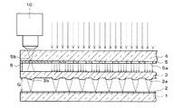
図6は従来のマイクロレンズアレイを使用した投影露光型の露光装置を示す断面図である。基板1上にレジスト膜2が形成されており、この基板1がマイクロレンズ露光装置の下方に搬送されてくる。従来のマイクロレンズ露光装置においては、多数のマイクロレンズ3aが2次元的に配置されて形成されたマイクロレンズアレイ3が設けられており、このマイクロレンズアレイ3の上方にマスク4が配置されている。マイクロレンズアレイ3は透明石英基板により形成されており、このマイクロレンズアレイ3の下面にマイクロレンズ3aが加工されている。マスク4は、透明基板の下面にCr膜5が接合されて構成されており、このCr膜5には、各マイクロレンズ3aに整合する位置にレーザ光が通過する孔5aが形成されている。このマスク4における孔5a以外の部分は、Cr膜5により覆われていて、レーザ光の通過を阻止する遮光部分となっている。このマスク4とマイクロレンズアレイ3とは、固定部材6により一定の間隔になるように固定されている。マイクロレンズアレイ3及びマスク4は適宜の駆動装置により光軸方向に移動可能であり、基板1との間の距離を調整することができるようになっている。
FIG. 6 is a sectional view showing a projection exposure type exposure apparatus using a conventional microlens array. A
このように構成された従来のマイクロレンズ露光装置においては、露光用のレーザ光をマスク4上に照射すると、マスク4の孔5aを通過したレーザ光が、マイクロレンズアレイ3の各マイクロレンズ3aに入射し、各マイクロレンズ3aにより基板1上のレジスト膜2に収束する。なお、この孔5aには、投影すべきパターンが形成されており、レーザ光が孔5aを透過してレジスト膜2に照射されたときに、前記パターンがレジスト膜2に投影される。
In the conventional microlens exposure apparatus configured as described above, when the exposure laser beam is irradiated onto the mask 4, the laser beam that has passed through the
このマイクロレンズ3aを通過したレーザ光を基板1の表面上のレジスト膜2に収束させるためには、基板1とマイクロレンズアレイ3との間のギャップGをマイクロレンズ3aの焦点位置に一致させる必要があり、このギャップGを管理する必要がある。従来の投影露光型露光装置においては、マスク4の表面と、基板1の表面との間の距離を測定して、それを所定値に設定することにより、ギャップGを管理していた。しかしながら、マイクロレンズが形成された石英基板の厚さは、製造条件により異なるため、従来においては、基板1とマイクロレンズ3aとの間のギャップGの管理は行っていないのが実情であった。このため、従来の露光装置においては、マスク4の表面と基板1の表面との間の距離を所定値に設定した後、露光し、現像してみて、得られたパターンを顕微鏡により観察することにより、基板1上のレジスト膜2がマイクロレンズ3aの合焦点位置にあるか否かを検査し、基板1がマイクロレンズ3aの合焦点位置にない場合は、マスク4及びマイクロレンズアレイ3の位置を調整し、再度、露光、現像、顕微鏡観察を実施して合焦点位置を確認するというような試行錯誤により、フォーカス調整を行っていた。このため、従来の露光装置においては、ギャップGの管理に大きな手間がかかっていた。
In order to converge the laser light that has passed through the
そこで、特許文献1においては、精度良く焦点位置に合わせることを目的とした画像露光装置が提案されている。この画像露光装置においては、焦点位置検出用のマイクロレンズを画像露光用のマイクロレンズとは別に設け、光源からのレーザ光を焦点位置検出用のマイクロレンズにも透過させて、レジスト膜上の結像位置に結像させるものである。そして、この像をカメラによって撮像し、撮像画像のピントが合うようにマイクロレンズアレイの位置を光軸方向に調整する。
Therefore,
しかしながら、上述の従来技術においては、図6に示すように、マイクロレンズアレイ3の上方にマスク4がマイクロレンズアレイ3に対して所定の間隔で配置された露光装置において、マイクロレンズアレイ3と基板1との間の間隔を調整するものではない。即ち、図6に示す従来の露光装置においては、上記特許文献1のギャップGの調整方法を適用することはできない。換言すれば、特許文献1の露光装置においては、マスク4が存在しないので、マイクロレンズアレイの表面の位置を直接検出できるため、このマイクロレンズアレイと基板表面との間のギャップを調整することに困難性はない。
However, in the above-described prior art, as shown in FIG. 6, in the exposure apparatus in which the mask 4 is arranged above the
本発明はかかる問題点に鑑みてなされたものであって、マイクロレンズアレイとマスクが所定間隔をおいて固定された露光装置において、マイクロレンズアレイと露光用基板との間のギャップを容易に高精度でマイクロレンズの合焦点位置に調整することができるマイクロレンズ露光装置を提供することを目的とする。 The present invention has been made in view of such problems, and in an exposure apparatus in which a microlens array and a mask are fixed at a predetermined interval, the gap between the microlens array and the exposure substrate can be easily increased. It is an object of the present invention to provide a microlens exposure apparatus that can be adjusted to the in-focus position of a microlens with accuracy.
本発明に係る第1のマイクロレンズ露光装置は、マイクロレンズが1次元又は2次元に配置されたマイクロレンズアレイと、各マイクロレンズに対応する位置にレーザ光の透過孔が設けられたマスクと、前記マイクロレンズアレイ及び前記マスクを相互に離隔した所定の間隔で固定する固定部と、を有するマイクロレンズ露光装置において、前記マイクロレンズアレイに設けられ前記マイクロレンズと同一形状の検査用マイクロレンズと、前記マスクにおける前記検査用マイクロレンズに対応する位置に設けられた検査用孔と、前記マスクの上方に設けられ前記検査用孔に焦点位置を合わせた検査用光を前記検査用孔及び前記検査用マイクロレンズを介して露光対象の基板に照射する検査用光照射部と、前記基板における前記検査用光の画像を観察する顕微鏡とを有し、前記顕微鏡により観察した画像が合焦点になるように前記マイクロレンズアレイ及び前記マスクの光軸上の位置を調整するものであることを特徴とする。 A first microlens exposure apparatus according to the present invention includes a microlens array in which microlenses are arranged one-dimensionally or two-dimensionally, a mask provided with a laser light transmission hole at a position corresponding to each microlens, A microlens exposure apparatus having a fixing unit that fixes the microlens array and the mask at predetermined intervals apart from each other , and an inspection microlens having the same shape as the microlens provided in the microlens array, An inspection hole provided at a position corresponding to the inspection microlens in the mask, and an inspection light provided above the mask and having a focal position aligned with the inspection hole An inspection light irradiation unit that irradiates a substrate to be exposed through a microlens, and an image of the inspection light on the substrate And a viewing microscopic, and wherein the image observed by the microscope is used to adjust the position on the optical axis of the microlens array and the mask so that the focal point.
この場合に、前記検査用孔に、検査用マークを設け、前記顕微鏡により、前記基板の画像と、前記検査用孔に設けた前記検査用マークの画像とを観察し、双方の画像が合焦点となるように、前記マイクロレンズアレイ及び前記マスクの光軸上の位置を調整することもできる。 In this case, an inspection mark is provided in the inspection hole, and the image of the substrate and the image of the inspection mark provided in the inspection hole are observed by the microscope, and both images are in focus. The positions of the microlens array and the mask on the optical axis can be adjusted so that
本発明に係る第2のマイクロレンズ露光装置は、マイクロレンズが1次元又は2次元に配置されたマイクロレンズアレイと、各マイクロレンズに対応する位置にレーザ光の透過孔が設けられたマスクと、前記マイクロレンズアレイ及び前記マスクを相互に離隔した所定の間隔で固定する固定部と、を有するマイクロレンズ露光装置において、前記マイクロレンズアレイに設けられ前記マイクロレンズと同一形状の検査用マイクロレンズと、前記マスクにおける前記検査用マイクロレンズに対応する位置に設けられた検査用孔と、前記マスクの上方に設けられ前記検査用孔に焦点位置を合わせた検査用光を前記検査用孔及び前記検査用マイクロレンズを介して露光対象の基板に照射する検査用光照射部と、前記基板で反射した前記検査用光の光量を検出するフォトセンサとを有し、前記フォトセンサで検出した光量が最大になるように前記マイクロレンズアレイ及び前記マスクの光軸上の位置を調整するものであることを特徴とする。 A second microlens exposure apparatus according to the present invention includes a microlens array in which microlenses are arranged one-dimensionally or two-dimensionally, a mask provided with a laser light transmission hole at a position corresponding to each microlens, A microlens exposure apparatus having a fixing unit that fixes the microlens array and the mask at predetermined intervals apart from each other , and an inspection microlens having the same shape as the microlens provided in the microlens array, An inspection hole provided at a position corresponding to the inspection microlens in the mask, and an inspection light provided above the mask and having a focal position aligned with the inspection hole are provided for the inspection hole and the inspection Inspection light irradiating unit that irradiates the substrate to be exposed through the microlens, and light of the inspection light reflected by the substrate And a photo sensor for detecting a, and wherein the amount of light detected by the photosensor is used to adjust the position on the optical axis of the microlens array and the mask so as to maximize.
本発明に係る第3のマイクロレンズ露光装置は、マイクロレンズが1次元又は2次元に配置されたマイクロレンズアレイと、各マイクロレンズに対応する位置にレーザ光の透過孔が設けられたマスクと、前記マイクロレンズアレイ及び前記マスクを相互に離隔した所定の間隔で固定する固定部と、を有するマイクロレンズ露光装置において、前記マイクロレンズアレイに設けられ前記マイクロレンズと同一形状の検査用マイクロレンズと、前記マスクにおける前記検査用マイクロレンズに対応する位置に設けられた検査用孔と、露光対象に設けたパターンに平行光の検査用光を照射して前記検査用マイクロレンズに前記パターンを透過した画像を入射させる検査用光照射部と、前記パターンを透過した画像を観察する顕微鏡とを有し、前記顕微鏡により観察した画像が合焦点になるように前記マイクロレンズアレイ及び前記マスクの光軸上の位置を調整するものであることを特徴とする。 A third microlens exposure apparatus according to the present invention includes a microlens array in which microlenses are arranged one-dimensionally or two-dimensionally, a mask provided with a laser light transmission hole at a position corresponding to each microlens, A microlens exposure apparatus having a fixing unit that fixes the microlens array and the mask at predetermined intervals apart from each other , and an inspection microlens having the same shape as the microlens provided in the microlens array, An image obtained by irradiating an inspection hole provided at a position corresponding to the inspection microlens in the mask and a pattern provided on an exposure target with parallel inspection light and transmitting the pattern through the inspection microlens And a microscope for observing an image transmitted through the pattern. And wherein the image observed by the mirror is used to adjust the position on the optical axis of the microlens array and the mask so that the focal point.
この場合に、前記検査用孔に、検査用マークを設け、前記顕微鏡により、前記パターンを透過した画像と、前記検査用孔に設けた前記検査用マークを透過した画像とを観察し、双方の画像が合焦点となるように、前記マイクロレンズアレイ及び前記マスクの光軸上の位置を調整することもできる。 In this case, an inspection mark is provided in the inspection hole, and an image transmitted through the pattern and an image transmitted through the inspection mark provided in the inspection hole are observed by the microscope. The positions of the microlens array and the mask on the optical axis can be adjusted so that the image is in focus.
本発明に係る第4のマイクロレンズ露光装置は、マイクロレンズが1次元又は2次元に配置されたマイクロレンズアレイと、各マイクロレンズに対応する位置にレーザ光の透過孔が設けられたマスクと、前記マイクロレンズアレイ及び前記マスクを相互に離隔した所定の間隔で固定する固定部と、を有するマイクロレンズ露光装置において、前記マイクロレンズアレイに設けられ前記マイクロレンズと同一形状の検査用マイクロレンズと、前記マスクにおける前記検査用マイクロレンズに対応する位置に設けられた検査用孔と、露光対象に設けたパターンに平行光の検査用光を照射して前記検査用マイクロレンズに前記パターンを透過した画像を入射させる検査用光照射部と、前記パターンを透過した前記検査用光の光量を検出するフォトセンサとを有し、前記フォトセンサで検出した光量が最大になるように前記マイクロレンズアレイ及び前記マスクの光軸上の位置を調整するものであることを特徴とする。
A fourth microlens exposure apparatus according to the present invention includes a microlens array in which microlenses are arranged one-dimensionally or two-dimensionally, a mask provided with a laser light transmission hole at a position corresponding to each microlens, A microlens exposure apparatus having a fixing unit that fixes the microlens array and the mask at predetermined intervals apart from each other , and an inspection microlens having the same shape as the microlens provided in the microlens array, An image obtained by irradiating an inspection hole provided at a position corresponding to the inspection microlens in the mask and a pattern provided on an exposure target with parallel inspection light and transmitting the pattern through the inspection microlens An inspection light irradiating unit for injecting the light, and a photosensor for detecting the amount of the inspection light transmitted through the pattern. And a support, wherein the amount of light detected by the photosensor is used to adjust the position on the optical axis of the microlens array and the mask so as to maximize.
本発明によれば、マスクに設けた検査用孔に合焦点した検査用光を検査用マイクロレンズを介して露光基板に照射し、顕微鏡により観察した検査用光の基板上の画像が合焦点するように、又はフォトセンサにより検出した前記検査用光の前記基板における反射光の光量が最大となるように、前記マイクロレンズアレイと前記基板との間隔を調整するので、極めて容易にかつ高精度で前記マイクロレンズの位置を合焦点位置に調節することができる。 According to the present invention, the inspection light focused on the inspection hole provided in the mask is irradiated to the exposure substrate through the inspection microlens, and the image on the substrate of the inspection light observed by the microscope is focused. Or the interval between the microlens array and the substrate is adjusted so that the amount of reflected light of the inspection light detected by the photosensor on the substrate is maximized, so that it is extremely easy and highly accurate. The position of the microlens can be adjusted to the in-focus position.
以下、本発明の実施の形態について、添付の図面を参照して具体的に説明する。図1は本発明の第1実施形態に係るマイクロレンズ露光装置を示す模式図である。図1において、図6と同一構成物には同一符号を付して、その詳細な説明は省略する。本実施形態においては、マイクロレンズアレイ3における端部のマイクロレンズ3aからなる露光領域から外れる位置に、検査用のマイクロレンズ3bが設けられ、更に、マスク4のCr膜5におけるマイクロレンズ3bに整合する位置に、孔5aよりも小さい孔5bが設けられている。孔5aには、投影すべきパターンが形成されており、レーザ光が孔5aを透過してレジスト膜2に照射されたときに、前記パターンがレジスト膜2に投影される。そして、マスク4の上方に顕微鏡10がマスク4及びマイクロレンズアレイ3に対して固定的に設けられている。この顕微鏡10の焦点位置は、マスク4の孔5bの位置であり、マイクロレンズアレイ3のマイクロレンズ3aを透過したレーザ光が基板1上のレジスト膜2で結像したときには、マイクロレンズ3bを透過した光も基板1上のレジスト膜2に結像する。従って、レジスト膜2にマーク(図示せず)を設けておくことにより、顕微鏡10からこのマークを観察し、顕微鏡10において、観察したマークの焦点が合っていれば、レジスト膜2の光軸上の位置は、顕微鏡10における合焦点の位置にあることになる。なお、本実施形態においても、マイクロレンズアレイ3及びマスク4は適宜の駆動装置により光軸方向に移動可能であり、基板1との間の距離を調整することができるようになっているが、顕微鏡10はマイクロレンズアレイ3及びマスク4に対して固定的に配置されているので、顕微鏡10からの光の焦点位置は、マスク4のCr膜5の孔5bの位置から変化しない。なお、顕微鏡10は、落射型顕微鏡であり、光源からの光が対物レンズから平行光となって基板上(レジスト膜2上)に照射され、基板(レジスト膜)からの反射光がマイクロレンズ3bにより検査用孔5bにて焦点を結び、その後、対物レンズから出射光と同軸的に入射されて、この入射光を観察するようになっている。この対物レンズからの入射光はカメラ等により撮影することもできる。よって、本実施形態においては、落射顕微鏡が、検査用光の光源と画像観察用の顕微鏡とを兼ねる。
Hereinafter, embodiments of the present invention will be specifically described with reference to the accompanying drawings. FIG. 1 is a schematic view showing a microlens exposure apparatus according to the first embodiment of the present invention. In FIG. 1, the same components as those in FIG. 6 are denoted by the same reference numerals, and detailed description thereof is omitted. In the present embodiment, a
このように構成された第1実施形態のマイクロレンズ露光装置においては、基板1上のレジスト膜2をマイクロレンズアレイ3のマイクロレンズ3aにより露光するが、このとき、顕微鏡10から平行光の落射照明光が検査用孔5bに向けて出射され、この落射照明光は、Cr膜5の孔5bで焦点を結び、この孔5bを通過してマイクロレンズアレイ3に向けて照射され、マイクロレンズ3bによりレジスト膜2に結像し、この反射光がマイクロレンズ3bにより孔5bの位置で結像し、この孔5bを通過して顕微鏡10に入射する。このとき、顕微鏡10に入射してきたレジスト膜2からの反射光が、レジスト膜2上で合焦点であった場合には、顕微鏡10で観察した像も焦点が合ったものとなる。これにより、露光領域のマイクロレンズ3aを透過したレーザ光も、レジスト膜2上で合焦点となる。
In the microlens exposure apparatus of the first embodiment configured as described above, the resist
よって、顕微鏡10で観察したレジスト膜2の画像が合焦点画像でなかった場合は、適宜の駆動装置によりマイクロレンズアレイ3及びマスク4を顕微鏡10と共に光軸方向に移動させ、顕微鏡10により画像を観察して、その画像が合焦点となる光軸上の位置を探せばよい。これにより、露光装置のギャップGを所定の合焦点位置に、容易にかつ高精度で調整することができる。
Therefore, when the image of the resist
なお、図4(a)、(b)に示すように、検査用孔5bに、検査用マーク22を設けることもできる。図4(b)の断面図に示す露光装置においては、検査用孔5b内に検査用マーク22が形成されていると共に、基板1の表面上のレジスト膜2の上に基板パターン21が設けられている。そして、落射照明光の平行光が孔5bを透過した後、マイクロレンズ3bにより収束されて基板パターン21に焦点を結ぶ。この場合に、図4(a)に示すように、基板パターン21はマイクロレンズ3bの視野領域20の中心に設けられた例えば円形のパターンであり、検査用マーク22は、マイクロレンズ3bの視野領域20の外側に、視野領域20の中心から4方向に放射状に延びる線分状に形成されている。
As shown in FIGS. 4A and 4B, an
そして、顕微鏡10により、基板1のレジスト膜2上のパターン21の画像と、検査用孔5bに設けた検査用マーク22の画像とを同時に観察し、双方の画像が合焦点となるように、マイクロレンズアレイ3及びマスク4の光軸上の位置を調整する。これにより、合焦点の精度を高めることができる。図1に示す実施形態では、顕微鏡10からの検査用光が孔5bで焦点を結ぶような位置に、顕微鏡10とマスク4とが機械的に固定されているが、図4に示す変形例においては、顕微鏡10とマスク4とは最終的には固定されるものの、先ず、検査用マーク22の焦点を合わせることにより、顕微鏡10とマスク4との位置関係を調整した後、両者を固定し、その後、基板上の基板パターン21に焦点が合うように、マイクロレンズアレイ3及びマスク4と基板1との間隔を調整するようにすることができる。
Then, the
なお、上述のように、基板1上のレジスト膜2の面に形成するマーク(パターン21)は、例えば、円形の点状マークであり、マスク4の検査用孔5bに形成するマーク(検査用マーク22)は、放射状に延びる線分状のマークであるが、これらのパターン21及び検査用マーク22は上記形状に限らないことはもちろんである。但し、検査用孔5bに形成する検査用マーク22はマイクロレンズ3bの視野領域20から外れた位置に設ける必要がある。検査用マーク22がマイクロレンズ3bの視野領域内に位置すると、顕微鏡10からマイクロレンズ3bに向けて照射される平行光の落射照明光を遮光してしまい、基板1のレジスト膜2上に照射される照明光の光量が低下する。
As described above, the mark (pattern 21) formed on the surface of the resist
次に、本発明の第2実施形態について説明する。図2は、本実施形態を示す断面図である。本実施形態は、第1実施形態の顕微鏡10の代わりに、フォトセンサ11を設けたものである。このフォトセンサ11もマイクロレンズアレイ3及びマスク4に対して固定的に設けられており、フォトセンサ11からは、孔5bに焦点位置を合わせた光がマイクロレンズ3bに向けて照射される。
Next, a second embodiment of the present invention will be described. FIG. 2 is a cross-sectional view showing this embodiment. In the present embodiment, a
次に、本実施形態の動作について説明する。フォトセンサ11からの光は、孔5bで焦点を結んだ後、拡大してマイクロレンズ3bに入射し、更にマイクロレンズ3bにより収束して、基板1上のレジスト膜2上に照射される。このレジスト膜2で反射した光は、マイクロレンズ3b及び孔5bを介してフォトセンサ11によりその光量が検出される。このとき、この光が、レジスト膜2上で合焦点であった場合には、その反射光は、孔5bにおいて焦点を結んだ後、フォトセンサ11に入射する。従って、その検出光量は多い。これに対し、レジスト膜2に入射した光が、レジスト膜2上で合焦点でなかった場合には、その反射光は孔5bで焦点を結ばず、拡散した状態であるので、その一部は孔5bの周囲のCr膜5により遮光されて、フォトセンサ11には入射しない。よって、この場合は、フォトセンサ11の検出光量は低下する。よって、フォトセンサ11にて反射光の光量を測定した場合に、その検出光量が最大となるときが、マイクロレンズアレイ3のマイクロレンズ3a、3bを透過した光が、レジスト膜2上で合焦点となる状態である。従って、フォトセンサ11の検出光量が最大となるように、マイクロレンズアレイ3及びマスク4の光軸上の位置を調整すれば、マイクロレンズアレイ3と基板1との間のギャップGを所定値に容易に且つ高精度で調整することができる。
Next, the operation of this embodiment will be described. The light from the
次に、本発明の第3実施形態について説明する。図3は、本実施形態を示す断面図である。本実施形態は、第1実施形態の落射型顕微鏡10の代わりに、透過型顕微鏡13を使用したものである。また、基板12は透明基板であり、レジスト膜2における焦点を結ぶべき位置に、パターン14が形成されている。そして、この透明基板12の下面から平行光がパターン14に向けて照射される。
Next, a third embodiment of the present invention will be described. FIG. 3 is a cross-sectional view showing this embodiment. In this embodiment, a transmission microscope 13 is used instead of the epi-
パターン14は、円又は縞模様等の形状を有し、透明基板12の下面から照射される平行光がこのパターン14を通過し、マイクロレンズ3bにより、パターン14の像が孔5bの位置に結像する。
The
次に、このように構成されたマイクロレンズ露光装置の動作について説明する。透明基板12の下面から平行光をパターン14に向けて照射すると、このパターン14を透過した光がマイクロレンズ3bにより収束されて、孔5bの位置に結像し、更に、透過型顕微鏡13の対物レンズを介して透過型顕微鏡13内に入射する。この透過型顕微鏡13に入射したパターン14の像を観察することにより、ギャップGが所定の焦点位置にあるか否かが判別される。即ち、ギャップGがマイクロレンズ3bの焦点距離である場合、パターン14の像はマイクロレンズ3bにより孔5bの位置に合焦点する。そうすると、透過型顕微鏡13の対物レンズに入射したパターン透過光は透過型顕微鏡13の接眼レンズで合焦点と観察され、又はカメラのCCD(電荷結合素子)に結像する。しかし、ギャップGが所定の焦点距離でないと、パターン14を透過した光は、マイクロレンズ3bにより孔5bにて合焦点することはなく、透過型顕微鏡13において焦点が合っていない画像として観察される。このようにして、透過型顕微鏡13にて、レジスト膜2上のパターン14を観察して、ギャップGを調整することにより、このギャップGをマイクロレンズ3aの焦点位置がレジスト膜2上になるように調節することができる。
Next, the operation of the thus configured microlens exposure apparatus will be described. When parallel light is irradiated from the lower surface of the
図5(a)、(b)は図4と同様に、透明基板12上のレジスト膜2上に基板パターン21を設けると共に、更に検査用孔5b内に検査用マーク23を設けたものであり、図3の第3実施形態の変形例である。但し、本変形例の場合は、マイクロレンズ3bの視野領域20内に検査用孔5b内の検査用マーク23も設けている。基板パターン21は、例えば、マイクロレンズ3bの視野領域20の中心に配置された円形のパターンであり、検査用マーク23は、例えば、基板パターン21を中心に4方向に放射状に延びる線分状のパターンである。
5A and 5B, as in FIG. 4, a
本変形例においては、透明基板12の下面側から照射された平行光の透過照明光は、基板12上のレジスト膜2上の基板パターン21により遮光されてマイクロレンズ3bに入射し、パターン21の像は、マイクロレンズ3bにより収束されて検査用孔5bにて合焦点となる。そして、このパターン21の像は対物レンズを介して透過型顕微鏡13に入射し、接写レンズにて観察され、又はカメラに撮影される。一方、マイクロレンズ3bの視野領域内にある検査用マーク23も透過照明光が照射されて、検査用マーク23の像も透過型顕微鏡13に入射する。
In this modification, the transmitted illumination light of the parallel light irradiated from the lower surface side of the
そして、本変形例においても、顕微鏡13により、基板12のレジスト膜2上のパターン21の画像と、検査用孔5bに設けた検査用マーク23の画像とを同時に観察し、双方の画像が合焦点となるように、マイクロレンズアレイ3及びマスク4の光軸上の位置を調整する。これにより、合焦点の精度を高めることができる。なお、本変形例の場合は、基板12の裏面から照射される透過照明により、基板パターン21及び検査用マスク23の像が合焦点であるか否かを判断するので、検査用マスク23は、マイクロレンズ3bの視野領域内に形成することができる。
Also in this modification, the microscope 13 simultaneously observes the image of the
なお、図3に示す実施形態において、透過型顕微鏡13による画像の合焦点の観察の代わりに、図2に示す実施形態と同様に、フォトセンサにより検出光量を測定して、ギャップGがマイクロレンズ3aの焦点距離に一致しているか否かの判定をすることもできる。透明基板12の下面から平行光を照射し、パターン14を透過した光を、マイクロレンズ3bにより収束させ、孔5bを通過した光をフォトセンサ11(図2参照)に導き、フォトセンサ11により最大光量が得られるか否かにより、ギャップGが所定の焦点位置にあるか否かを判別することができる。ギャップGが所定の焦点距離であって、マイクロレンズ3aからのレーザ光がレジスト膜2上で合焦点にあれば、透明基板12の下面からパターン14に照射されてパターン14を透過した光は、マイクロレンズ3bにより孔5bで焦点を結び、小さな孔5bを通過してその殆どの光量がフォトセンサ11に検出されるが、ギャップGが焦点位置からずれている場合は、パターン14を透過した光は、マイクロレンズ3bにより孔5bにて合焦点とならず、孔5bの周囲のCr膜5の部分まで拡がってしまい、小さな孔5bを通過する光の光量は低下する。従って、フォトセンサ11にて光量を測定し、マスク4及びマイクロレンズアレイ3を光軸方向に移動させて、その検出光量が最大となった状態が、ギャップGがマイクロレンズ3aの焦点距離と一致し、マイクロレンズ3aにより収束されたレーザ光がレジスト膜2上で合焦点となる。
In the embodiment shown in FIG. 3, instead of observing the in-focus point of the image with the transmission microscope 13, the detected light quantity is measured by a photosensor as in the embodiment shown in FIG. It can also be determined whether or not it matches the
上記各実施形態は、レジスト膜に所定のパターンを露光する露光装置についてのものであるが、本発明は、アモルファスシリコン膜をレーザ光により露光してアニールすることにより低温ポリシリコン膜を形成するようなアニール装置にも適用することができる。 Each of the above embodiments relates to an exposure apparatus that exposes a predetermined pattern on a resist film. However, the present invention forms a low-temperature polysilicon film by exposing an amorphous silicon film to a laser beam and annealing it. It can be applied to any annealing apparatus.
1:基板
2:レジスト膜
3:マイクロレンズアレイ
3a,3b:マイクロレンズ
4:マスク
5:Cr膜
5a、5b:孔
6:固定部材
10;顕微鏡(落射型)
11:フォトセンサ
12:透明基板
13:透過型顕微鏡
14:パターン
21:パターン
22,23:検査用マーク
1: Substrate 2: Resist film 3:
11: Photosensor 12: Transparent substrate 13: Transmission microscope 14: Pattern 21:
Claims (6)
Priority Applications (6)
| Application Number | Priority Date | Filing Date | Title |
|---|---|---|---|
| JP2010177873A JP5424267B2 (en) | 2010-08-06 | 2010-08-06 | Micro lens exposure system |
| PCT/JP2011/066217 WO2012017808A1 (en) | 2010-08-06 | 2011-07-15 | Microlens exposure device |
| US13/813,130 US9429852B2 (en) | 2010-08-06 | 2011-07-15 | Microlens exposure system |
| CN201180038786.0A CN103026458B (en) | 2010-08-06 | 2011-07-15 | Lenticule exposure device |
| KR1020137005682A KR101820999B1 (en) | 2010-08-06 | 2011-07-15 | Microlens exposure device |
| TW100127437A TWI529498B (en) | 2010-08-06 | 2011-08-02 | Micro-lens exposure device |
Applications Claiming Priority (1)
| Application Number | Priority Date | Filing Date | Title |
|---|---|---|---|
| JP2010177873A JP5424267B2 (en) | 2010-08-06 | 2010-08-06 | Micro lens exposure system |
Publications (3)
| Publication Number | Publication Date |
|---|---|
| JP2012038927A JP2012038927A (en) | 2012-02-23 |
| JP2012038927A5 JP2012038927A5 (en) | 2012-04-05 |
| JP5424267B2 true JP5424267B2 (en) | 2014-02-26 |
Family
ID=45559315
Family Applications (1)
| Application Number | Title | Priority Date | Filing Date |
|---|---|---|---|
| JP2010177873A Expired - Fee Related JP5424267B2 (en) | 2010-08-06 | 2010-08-06 | Micro lens exposure system |
Country Status (6)
| Country | Link |
|---|---|
| US (1) | US9429852B2 (en) |
| JP (1) | JP5424267B2 (en) |
| KR (1) | KR101820999B1 (en) |
| CN (1) | CN103026458B (en) |
| TW (1) | TWI529498B (en) |
| WO (1) | WO2012017808A1 (en) |
Families Citing this family (10)
| Publication number | Priority date | Publication date | Assignee | Title |
|---|---|---|---|---|
| JP5376379B2 (en) * | 2010-08-30 | 2013-12-25 | 株式会社ブイ・テクノロジー | Exposure apparatus and optical member using microlens array |
| FR3014212B1 (en) * | 2013-12-04 | 2017-05-26 | Fogale Nanotech | DEVICE AND METHOD FOR POSITIONING PHOTOLITHOGRAPHY MASK BY OPTICAL NON-CONTACT METHOD |
| CN104865801B (en) * | 2015-06-01 | 2017-03-01 | 京东方科技集团股份有限公司 | Exposure device |
| US10761192B2 (en) * | 2015-08-28 | 2020-09-01 | Ams Sensors Singapore Pte. Ltd. | Illumination modules for translating light |
| WO2017170392A1 (en) * | 2016-03-30 | 2017-10-05 | 株式会社ニコン | Optical device |
| CN107843966B (en) * | 2016-09-18 | 2021-05-04 | 中芯国际集成电路制造(上海)有限公司 | Method and system for assembling microlens array assembly |
| EP3553462B1 (en) * | 2016-12-12 | 2021-05-26 | National Institute of Advanced Industrial Science and Technology | Marker and marker manufacturing method |
| US10270032B2 (en) * | 2017-09-13 | 2019-04-23 | Int Tech Co., Ltd. | Light source and a manufacturing method therewith |
| CN109062001B (en) * | 2018-08-27 | 2022-04-08 | 京东方科技集团股份有限公司 | Mask plate |
| JP7082927B2 (en) * | 2018-08-27 | 2022-06-09 | 株式会社Screenホールディングス | Exposure device |
Family Cites Families (12)
| Publication number | Priority date | Publication date | Assignee | Title |
|---|---|---|---|---|
| CH697814B1 (en) * | 2001-01-26 | 2009-02-27 | Tecan Trading Ag | Optical system and method for exciting and measuring fluorescence on or in samples treated with fluorescent dyes. |
| US4767171A (en) * | 1986-03-27 | 1988-08-30 | Siemens Aktiengesellschaft | Transmission and reception module for a bidirectional communication network |
| JPH0243511A (en) * | 1988-08-04 | 1990-02-14 | Fuji Electric Co Ltd | Method for aligning image sensor pair with optical system |
| JPH0320733A (en) * | 1989-06-16 | 1991-01-29 | Matsushita Electron Corp | Photomask |
| JP3555230B2 (en) | 1994-05-18 | 2004-08-18 | 株式会社ニコン | Projection exposure equipment |
| JP3374875B2 (en) * | 1994-06-21 | 2003-02-10 | 三菱電機株式会社 | Semiconductor photoengraving apparatus and fine pattern formed using the same |
| JP2002006208A (en) * | 2000-06-23 | 2002-01-09 | Asahi Optical Co Ltd | Digital still camera with automatic focus detecting mechanism |
| KR100877708B1 (en) * | 2001-03-29 | 2009-01-07 | 다이니폰 인사츠 가부시키가이샤 | Method of producing pattern-formed structure and photomask used in the same |
| JP2007003829A (en) * | 2005-06-23 | 2007-01-11 | Fujifilm Holdings Corp | Image exposure device |
| JP2009302400A (en) | 2008-06-16 | 2009-12-24 | Canon Inc | Exposure apparatus and method of manufacturing device |
| JP5381029B2 (en) | 2008-11-10 | 2014-01-08 | ウシオ電機株式会社 | Exposure equipment |
| CN103858208B (en) * | 2011-08-10 | 2016-08-24 | 株式会社V技术 | The alignment device of exposure device and alignment mark |
-
2010
- 2010-08-06 JP JP2010177873A patent/JP5424267B2/en not_active Expired - Fee Related
-
2011
- 2011-07-15 CN CN201180038786.0A patent/CN103026458B/en not_active Expired - Fee Related
- 2011-07-15 KR KR1020137005682A patent/KR101820999B1/en active IP Right Grant
- 2011-07-15 WO PCT/JP2011/066217 patent/WO2012017808A1/en active Application Filing
- 2011-07-15 US US13/813,130 patent/US9429852B2/en not_active Expired - Fee Related
- 2011-08-02 TW TW100127437A patent/TWI529498B/en not_active IP Right Cessation
Also Published As
| Publication number | Publication date |
|---|---|
| JP2012038927A (en) | 2012-02-23 |
| KR101820999B1 (en) | 2018-01-22 |
| CN103026458B (en) | 2015-11-25 |
| US9429852B2 (en) | 2016-08-30 |
| WO2012017808A1 (en) | 2012-02-09 |
| US20130141704A1 (en) | 2013-06-06 |
| KR20140002612A (en) | 2014-01-08 |
| TWI529498B (en) | 2016-04-11 |
| CN103026458A (en) | 2013-04-03 |
| TW201234117A (en) | 2012-08-16 |
Similar Documents
| Publication | Publication Date | Title |
|---|---|---|
| JP5424267B2 (en) | Micro lens exposure system | |
| JP2924344B2 (en) | Projection exposure equipment | |
| JP2012038927A5 (en) | ||
| JP2006078849A (en) | Lens system adjusting device and lens system adjusting method using the same | |
| JP6450392B2 (en) | Imaging device | |
| JP2006184777A (en) | Focus detector | |
| KR102026107B1 (en) | Light exposure device and method for manufacturing exposed material | |
| JPWO2012099034A1 (en) | Focus position maintaining device and microscope | |
| TW202235195A (en) | Observation device and observation method performing the moving of the condensing position at high speed even if imaging region is larger | |
| TW201248339A (en) | Alignment device for light exposure device | |
| JP6190168B2 (en) | Focusing method, focusing apparatus, exposure method, and device manufacturing method | |
| JP2630302B2 (en) | Substrate position determination method and projection exposure method in projection optical system | |
| JP5874900B2 (en) | Alignment device for exposure equipment | |
| WO2006046430A1 (en) | Focal point detection device | |
| TW202009081A (en) | Laser processing apparatus | |
| JP5953038B2 (en) | Apparatus and method for measuring focal length of microlens array | |
| JP7036396B1 (en) | Autofocus device | |
| JP5288477B2 (en) | Exposure equipment | |
| JP2008224737A (en) | Optical substrate, and position shift measuring method for substrate top/reverse surface pattern using positioning pattern | |
| WO2012133903A1 (en) | Alignment device for exposure device | |
| JPH09260269A (en) | Method of projection exposure and production method of device using it | |
| JP2008232689A (en) | Positional misalignment measuring method of substrate front/back surface pattern using opening pattern | |
| JP2004342642A (en) | Position detector for detecting edge scattering light obliquely | |
| JP2004264127A (en) | Mark position detector | |
| JP2022095051A (en) | Exposure device, exposure method and manufacturing method of article |
Legal Events
| Date | Code | Title | Description |
|---|---|---|---|
| A521 | Written amendment |
Free format text: JAPANESE INTERMEDIATE CODE: A523 Effective date: 20111226 |
|
| A621 | Written request for application examination |
Free format text: JAPANESE INTERMEDIATE CODE: A621 Effective date: 20130711 |
|
| A131 | Notification of reasons for refusal |
Free format text: JAPANESE INTERMEDIATE CODE: A131 Effective date: 20130806 |
|
| A521 | Written amendment |
Free format text: JAPANESE INTERMEDIATE CODE: A523 Effective date: 20130919 |
|
| TRDD | Decision of grant or rejection written | ||
| A01 | Written decision to grant a patent or to grant a registration (utility model) |
Free format text: JAPANESE INTERMEDIATE CODE: A01 Effective date: 20131105 |
|
| A61 | First payment of annual fees (during grant procedure) |
Free format text: JAPANESE INTERMEDIATE CODE: A61 Effective date: 20131120 |
|
| R150 | Certificate of patent or registration of utility model |
Free format text: JAPANESE INTERMEDIATE CODE: R150 Ref document number: 5424267 Country of ref document: JP Free format text: JAPANESE INTERMEDIATE CODE: R150 |
|
| R250 | Receipt of annual fees |
Free format text: JAPANESE INTERMEDIATE CODE: R250 |
|
| LAPS | Cancellation because of no payment of annual fees |