JP5417236B2 - Method for manufacturing lighting device - Google Patents
Method for manufacturing lighting device Download PDFInfo
- Publication number
- JP5417236B2 JP5417236B2 JP2010071754A JP2010071754A JP5417236B2 JP 5417236 B2 JP5417236 B2 JP 5417236B2 JP 2010071754 A JP2010071754 A JP 2010071754A JP 2010071754 A JP2010071754 A JP 2010071754A JP 5417236 B2 JP5417236 B2 JP 5417236B2
- Authority
- JP
- Japan
- Prior art keywords
- substrate
- film
- evaporation source
- film formation
- chamber
- Prior art date
- Legal status (The legal status is an assumption and is not a legal conclusion. Google has not performed a legal analysis and makes no representation as to the accuracy of the status listed.)
- Expired - Fee Related
Links
- 238000000034 method Methods 0.000 title claims description 28
- 238000004519 manufacturing process Methods 0.000 title claims description 5
- 239000000758 substrate Substances 0.000 claims description 155
- 239000000463 material Substances 0.000 claims description 132
- 238000001704 evaporation Methods 0.000 claims description 84
- 230000008020 evaporation Effects 0.000 claims description 82
- 230000015572 biosynthetic process Effects 0.000 claims description 74
- 238000010549 co-Evaporation Methods 0.000 claims description 4
- 239000010408 film Substances 0.000 description 145
- 239000010409 thin film Substances 0.000 description 33
- 238000000151 deposition Methods 0.000 description 26
- 230000008021 deposition Effects 0.000 description 24
- 238000000605 extraction Methods 0.000 description 12
- 238000002347 injection Methods 0.000 description 10
- 239000007924 injection Substances 0.000 description 10
- 239000002274 desiccant Substances 0.000 description 8
- 239000000203 mixture Substances 0.000 description 8
- 238000007789 sealing Methods 0.000 description 8
- 238000005401 electroluminescence Methods 0.000 description 6
- 239000011368 organic material Substances 0.000 description 6
- 239000004033 plastic Substances 0.000 description 6
- VYPSYNLAJGMNEJ-UHFFFAOYSA-N silicon dioxide Inorganic materials O=[Si]=O VYPSYNLAJGMNEJ-UHFFFAOYSA-N 0.000 description 5
- 238000007740 vapor deposition Methods 0.000 description 5
- 238000010586 diagram Methods 0.000 description 4
- 150000002894 organic compounds Chemical class 0.000 description 4
- 238000001771 vacuum deposition Methods 0.000 description 4
- 230000000295 complement effect Effects 0.000 description 3
- 239000012530 fluid Substances 0.000 description 3
- 238000010438 heat treatment Methods 0.000 description 3
- 230000002093 peripheral effect Effects 0.000 description 3
- 239000000126 substance Substances 0.000 description 3
- 239000002699 waste material Substances 0.000 description 3
- XKRFYHLGVUSROY-UHFFFAOYSA-N Argon Chemical compound [Ar] XKRFYHLGVUSROY-UHFFFAOYSA-N 0.000 description 2
- 239000004695 Polyether sulfone Substances 0.000 description 2
- 229910052581 Si3N4 Inorganic materials 0.000 description 2
- 238000005054 agglomeration Methods 0.000 description 2
- 230000002776 aggregation Effects 0.000 description 2
- QVQLCTNNEUAWMS-UHFFFAOYSA-N barium oxide Chemical compound [Ba]=O QVQLCTNNEUAWMS-UHFFFAOYSA-N 0.000 description 2
- 239000000919 ceramic Substances 0.000 description 2
- 239000003086 colorant Substances 0.000 description 2
- 150000001875 compounds Chemical class 0.000 description 2
- 238000005520 cutting process Methods 0.000 description 2
- 239000011521 glass Substances 0.000 description 2
- 229920001230 polyarylate Polymers 0.000 description 2
- 239000004417 polycarbonate Substances 0.000 description 2
- 229920000515 polycarbonate Polymers 0.000 description 2
- 229920006393 polyether sulfone Polymers 0.000 description 2
- 239000010453 quartz Substances 0.000 description 2
- 239000003566 sealing material Substances 0.000 description 2
- HQVNEWCFYHHQES-UHFFFAOYSA-N silicon nitride Chemical compound N12[Si]34N5[Si]62N3[Si]51N64 HQVNEWCFYHHQES-UHFFFAOYSA-N 0.000 description 2
- 229910052814 silicon oxide Inorganic materials 0.000 description 2
- 238000001179 sorption measurement Methods 0.000 description 2
- 229910021536 Zeolite Inorganic materials 0.000 description 1
- 239000005083 Zinc sulfide Substances 0.000 description 1
- 229910000287 alkaline earth metal oxide Inorganic materials 0.000 description 1
- 229910052786 argon Inorganic materials 0.000 description 1
- 230000005540 biological transmission Effects 0.000 description 1
- BRPQOXSCLDDYGP-UHFFFAOYSA-N calcium oxide Chemical compound [O-2].[Ca+2] BRPQOXSCLDDYGP-UHFFFAOYSA-N 0.000 description 1
- ODINCKMPIJJUCX-UHFFFAOYSA-N calcium oxide Inorganic materials [Ca]=O ODINCKMPIJJUCX-UHFFFAOYSA-N 0.000 description 1
- 239000000292 calcium oxide Substances 0.000 description 1
- 239000004020 conductor Substances 0.000 description 1
- 230000006866 deterioration Effects 0.000 description 1
- HNPSIPDUKPIQMN-UHFFFAOYSA-N dioxosilane;oxo(oxoalumanyloxy)alumane Chemical compound O=[Si]=O.O=[Al]O[Al]=O HNPSIPDUKPIQMN-UHFFFAOYSA-N 0.000 description 1
- 238000009826 distribution Methods 0.000 description 1
- 238000001125 extrusion Methods 0.000 description 1
- 239000007789 gas Substances 0.000 description 1
- 230000005525 hole transport Effects 0.000 description 1
- 239000012535 impurity Substances 0.000 description 1
- 239000011261 inert gas Substances 0.000 description 1
- 238000010030 laminating Methods 0.000 description 1
- 229910001120 nichrome Inorganic materials 0.000 description 1
- 230000003287 optical effect Effects 0.000 description 1
- 230000003252 repetitive effect Effects 0.000 description 1
- 239000000565 sealant Substances 0.000 description 1
- 229910002027 silica gel Inorganic materials 0.000 description 1
- 239000000741 silica gel Substances 0.000 description 1
- 229920002545 silicone oil Polymers 0.000 description 1
- 238000009751 slip forming Methods 0.000 description 1
- 229910000679 solder Inorganic materials 0.000 description 1
- 229920001187 thermosetting polymer Polymers 0.000 description 1
- 238000007738 vacuum evaporation Methods 0.000 description 1
- XLYOFNOQVPJJNP-UHFFFAOYSA-N water Chemical compound O XLYOFNOQVPJJNP-UHFFFAOYSA-N 0.000 description 1
- 239000010457 zeolite Substances 0.000 description 1
- 229910052984 zinc sulfide Inorganic materials 0.000 description 1
- DRDVZXDWVBGGMH-UHFFFAOYSA-N zinc;sulfide Chemical compound [S-2].[Zn+2] DRDVZXDWVBGGMH-UHFFFAOYSA-N 0.000 description 1
Images


Classifications
-
- C—CHEMISTRY; METALLURGY
- C23—COATING METALLIC MATERIAL; COATING MATERIAL WITH METALLIC MATERIAL; CHEMICAL SURFACE TREATMENT; DIFFUSION TREATMENT OF METALLIC MATERIAL; COATING BY VACUUM EVAPORATION, BY SPUTTERING, BY ION IMPLANTATION OR BY CHEMICAL VAPOUR DEPOSITION, IN GENERAL; INHIBITING CORROSION OF METALLIC MATERIAL OR INCRUSTATION IN GENERAL
- C23C—COATING METALLIC MATERIAL; COATING MATERIAL WITH METALLIC MATERIAL; SURFACE TREATMENT OF METALLIC MATERIAL BY DIFFUSION INTO THE SURFACE, BY CHEMICAL CONVERSION OR SUBSTITUTION; COATING BY VACUUM EVAPORATION, BY SPUTTERING, BY ION IMPLANTATION OR BY CHEMICAL VAPOUR DEPOSITION, IN GENERAL
- C23C14/00—Coating by vacuum evaporation, by sputtering or by ion implantation of the coating forming material
- C23C14/22—Coating by vacuum evaporation, by sputtering or by ion implantation of the coating forming material characterised by the process of coating
- C23C14/56—Apparatus specially adapted for continuous coating; Arrangements for maintaining the vacuum, e.g. vacuum locks
- C23C14/568—Transferring the substrates through a series of coating stations
-
- C—CHEMISTRY; METALLURGY
- C23—COATING METALLIC MATERIAL; COATING MATERIAL WITH METALLIC MATERIAL; CHEMICAL SURFACE TREATMENT; DIFFUSION TREATMENT OF METALLIC MATERIAL; COATING BY VACUUM EVAPORATION, BY SPUTTERING, BY ION IMPLANTATION OR BY CHEMICAL VAPOUR DEPOSITION, IN GENERAL; INHIBITING CORROSION OF METALLIC MATERIAL OR INCRUSTATION IN GENERAL
- C23C—COATING METALLIC MATERIAL; COATING MATERIAL WITH METALLIC MATERIAL; SURFACE TREATMENT OF METALLIC MATERIAL BY DIFFUSION INTO THE SURFACE, BY CHEMICAL CONVERSION OR SUBSTITUTION; COATING BY VACUUM EVAPORATION, BY SPUTTERING, BY ION IMPLANTATION OR BY CHEMICAL VAPOUR DEPOSITION, IN GENERAL
- C23C14/00—Coating by vacuum evaporation, by sputtering or by ion implantation of the coating forming material
- C23C14/06—Coating by vacuum evaporation, by sputtering or by ion implantation of the coating forming material characterised by the coating material
- C23C14/12—Organic material
-
- C—CHEMISTRY; METALLURGY
- C23—COATING METALLIC MATERIAL; COATING MATERIAL WITH METALLIC MATERIAL; CHEMICAL SURFACE TREATMENT; DIFFUSION TREATMENT OF METALLIC MATERIAL; COATING BY VACUUM EVAPORATION, BY SPUTTERING, BY ION IMPLANTATION OR BY CHEMICAL VAPOUR DEPOSITION, IN GENERAL; INHIBITING CORROSION OF METALLIC MATERIAL OR INCRUSTATION IN GENERAL
- C23C—COATING METALLIC MATERIAL; COATING MATERIAL WITH METALLIC MATERIAL; SURFACE TREATMENT OF METALLIC MATERIAL BY DIFFUSION INTO THE SURFACE, BY CHEMICAL CONVERSION OR SUBSTITUTION; COATING BY VACUUM EVAPORATION, BY SPUTTERING, BY ION IMPLANTATION OR BY CHEMICAL VAPOUR DEPOSITION, IN GENERAL
- C23C14/00—Coating by vacuum evaporation, by sputtering or by ion implantation of the coating forming material
- C23C14/22—Coating by vacuum evaporation, by sputtering or by ion implantation of the coating forming material characterised by the process of coating
- C23C14/24—Vacuum evaporation
- C23C14/246—Replenishment of source material
-
- C—CHEMISTRY; METALLURGY
- C23—COATING METALLIC MATERIAL; COATING MATERIAL WITH METALLIC MATERIAL; CHEMICAL SURFACE TREATMENT; DIFFUSION TREATMENT OF METALLIC MATERIAL; COATING BY VACUUM EVAPORATION, BY SPUTTERING, BY ION IMPLANTATION OR BY CHEMICAL VAPOUR DEPOSITION, IN GENERAL; INHIBITING CORROSION OF METALLIC MATERIAL OR INCRUSTATION IN GENERAL
- C23C—COATING METALLIC MATERIAL; COATING MATERIAL WITH METALLIC MATERIAL; SURFACE TREATMENT OF METALLIC MATERIAL BY DIFFUSION INTO THE SURFACE, BY CHEMICAL CONVERSION OR SUBSTITUTION; COATING BY VACUUM EVAPORATION, BY SPUTTERING, BY ION IMPLANTATION OR BY CHEMICAL VAPOUR DEPOSITION, IN GENERAL
- C23C14/00—Coating by vacuum evaporation, by sputtering or by ion implantation of the coating forming material
- C23C14/22—Coating by vacuum evaporation, by sputtering or by ion implantation of the coating forming material characterised by the process of coating
- C23C14/24—Vacuum evaporation
- C23C14/26—Vacuum evaporation by resistance or inductive heating of the source
-
- C—CHEMISTRY; METALLURGY
- C23—COATING METALLIC MATERIAL; COATING MATERIAL WITH METALLIC MATERIAL; CHEMICAL SURFACE TREATMENT; DIFFUSION TREATMENT OF METALLIC MATERIAL; COATING BY VACUUM EVAPORATION, BY SPUTTERING, BY ION IMPLANTATION OR BY CHEMICAL VAPOUR DEPOSITION, IN GENERAL; INHIBITING CORROSION OF METALLIC MATERIAL OR INCRUSTATION IN GENERAL
- C23C—COATING METALLIC MATERIAL; COATING MATERIAL WITH METALLIC MATERIAL; SURFACE TREATMENT OF METALLIC MATERIAL BY DIFFUSION INTO THE SURFACE, BY CHEMICAL CONVERSION OR SUBSTITUTION; COATING BY VACUUM EVAPORATION, BY SPUTTERING, BY ION IMPLANTATION OR BY CHEMICAL VAPOUR DEPOSITION, IN GENERAL
- C23C14/00—Coating by vacuum evaporation, by sputtering or by ion implantation of the coating forming material
- C23C14/22—Coating by vacuum evaporation, by sputtering or by ion implantation of the coating forming material characterised by the process of coating
- C23C14/50—Substrate holders
- C23C14/505—Substrate holders for rotation of the substrates
-
- F—MECHANICAL ENGINEERING; LIGHTING; HEATING; WEAPONS; BLASTING
- F21—LIGHTING
- F21K—NON-ELECTRIC LIGHT SOURCES USING LUMINESCENCE; LIGHT SOURCES USING ELECTROCHEMILUMINESCENCE; LIGHT SOURCES USING CHARGES OF COMBUSTIBLE MATERIAL; LIGHT SOURCES USING SEMICONDUCTOR DEVICES AS LIGHT-GENERATING ELEMENTS; LIGHT SOURCES NOT OTHERWISE PROVIDED FOR
- F21K9/00—Light sources using semiconductor devices as light-generating elements, e.g. using light-emitting diodes [LED] or lasers
- F21K9/20—Light sources comprising attachment means
- F21K9/23—Retrofit light sources for lighting devices with a single fitting for each light source, e.g. for substitution of incandescent lamps with bayonet or threaded fittings
-
- H—ELECTRICITY
- H01—ELECTRIC ELEMENTS
- H01L—SEMICONDUCTOR DEVICES NOT COVERED BY CLASS H10
- H01L21/00—Processes or apparatus adapted for the manufacture or treatment of semiconductor or solid state devices or of parts thereof
- H01L21/02—Manufacture or treatment of semiconductor devices or of parts thereof
- H01L21/02104—Forming layers
- H01L21/02365—Forming inorganic semiconducting materials on a substrate
- H01L21/02612—Formation types
- H01L21/02617—Deposition types
- H01L21/02631—Physical deposition at reduced pressure, e.g. MBE, sputtering, evaporation
-
- F—MECHANICAL ENGINEERING; LIGHTING; HEATING; WEAPONS; BLASTING
- F21—LIGHTING
- F21V—FUNCTIONAL FEATURES OR DETAILS OF LIGHTING DEVICES OR SYSTEMS THEREOF; STRUCTURAL COMBINATIONS OF LIGHTING DEVICES WITH OTHER ARTICLES, NOT OTHERWISE PROVIDED FOR
- F21V23/00—Arrangement of electric circuit elements in or on lighting devices
- F21V23/003—Arrangement of electric circuit elements in or on lighting devices the elements being electronics drivers or controllers for operating the light source, e.g. for a LED array
-
- F—MECHANICAL ENGINEERING; LIGHTING; HEATING; WEAPONS; BLASTING
- F21—LIGHTING
- F21Y—INDEXING SCHEME ASSOCIATED WITH SUBCLASSES F21K, F21L, F21S and F21V, RELATING TO THE FORM OR THE KIND OF THE LIGHT SOURCES OR OF THE COLOUR OF THE LIGHT EMITTED
- F21Y2105/00—Planar light sources
-
- F—MECHANICAL ENGINEERING; LIGHTING; HEATING; WEAPONS; BLASTING
- F21—LIGHTING
- F21Y—INDEXING SCHEME ASSOCIATED WITH SUBCLASSES F21K, F21L, F21S and F21V, RELATING TO THE FORM OR THE KIND OF THE LIGHT SOURCES OR OF THE COLOUR OF THE LIGHT EMITTED
- F21Y2115/00—Light-generating elements of semiconductor light sources
- F21Y2115/10—Light-emitting diodes [LED]
- F21Y2115/15—Organic light-emitting diodes [OLED]
-
- H—ELECTRICITY
- H10—SEMICONDUCTOR DEVICES; ELECTRIC SOLID-STATE DEVICES NOT OTHERWISE PROVIDED FOR
- H10K—ORGANIC ELECTRIC SOLID-STATE DEVICES
- H10K50/00—Organic light-emitting devices
- H10K50/10—OLEDs or polymer light-emitting diodes [PLED]
- H10K50/11—OLEDs or polymer light-emitting diodes [PLED] characterised by the electroluminescent [EL] layers
- H10K50/125—OLEDs or polymer light-emitting diodes [PLED] characterised by the electroluminescent [EL] layers specially adapted for multicolour light emission, e.g. for emitting white light
-
- H—ELECTRICITY
- H10—SEMICONDUCTOR DEVICES; ELECTRIC SOLID-STATE DEVICES NOT OTHERWISE PROVIDED FOR
- H10K—ORGANIC ELECTRIC SOLID-STATE DEVICES
- H10K50/00—Organic light-emitting devices
- H10K50/10—OLEDs or polymer light-emitting diodes [PLED]
- H10K50/19—Tandem OLEDs
-
- H—ELECTRICITY
- H10—SEMICONDUCTOR DEVICES; ELECTRIC SOLID-STATE DEVICES NOT OTHERWISE PROVIDED FOR
- H10K—ORGANIC ELECTRIC SOLID-STATE DEVICES
- H10K59/00—Integrated devices, or assemblies of multiple devices, comprising at least one organic light-emitting element covered by group H10K50/00
- H10K59/30—Devices specially adapted for multicolour light emission
- H10K59/32—Stacked devices having two or more layers, each emitting at different wavelengths
-
- H—ELECTRICITY
- H10—SEMICONDUCTOR DEVICES; ELECTRIC SOLID-STATE DEVICES NOT OTHERWISE PROVIDED FOR
- H10K—ORGANIC ELECTRIC SOLID-STATE DEVICES
- H10K71/00—Manufacture or treatment specially adapted for the organic devices covered by this subclass
- H10K71/10—Deposition of organic active material
- H10K71/16—Deposition of organic active material using physical vapour deposition [PVD], e.g. vacuum deposition or sputtering
Landscapes
- Chemical & Material Sciences (AREA)
- Engineering & Computer Science (AREA)
- Metallurgy (AREA)
- Organic Chemistry (AREA)
- Chemical Kinetics & Catalysis (AREA)
- Materials Engineering (AREA)
- Mechanical Engineering (AREA)
- Microelectronics & Electronic Packaging (AREA)
- Physics & Mathematics (AREA)
- General Engineering & Computer Science (AREA)
- Optics & Photonics (AREA)
- Condensed Matter Physics & Semiconductors (AREA)
- General Physics & Mathematics (AREA)
- Manufacturing & Machinery (AREA)
- Computer Hardware Design (AREA)
- Power Engineering (AREA)
- Electroluminescent Light Sources (AREA)
- Physical Vapour Deposition (AREA)
Description
本発明の一形態は成膜装置及び成膜方法に関する。 One embodiment of the present invention relates to a film formation apparatus and a film formation method.
有機材料の薄膜が積層されて成る有機エレクトロルミネセンス素子は、真空蒸着法を用いて作製されている。真空蒸着法は種々の薄膜形成に用いられる代表的な技術であるが、有機エレクトロルミネッセンス素子を作製するに当たっては、真空蒸着装置の構成に様々な工夫が加えられている。 An organic electroluminescence element formed by laminating thin films of organic materials is manufactured using a vacuum deposition method. The vacuum vapor deposition method is a typical technique used for forming various thin films, but various devices have been added to the configuration of the vacuum vapor deposition apparatus when producing an organic electroluminescence element.
例えば、蒸着速度を一定に保つために、有機材料を充填した容器と、有機材料を被着させる基板とを対向して設け、さらに容器と基板との空間を囲むように加熱壁が設けられた真空蒸着装置が開示されている(特許文献1参照)。
この真空蒸着装置は、加熱壁を有機材料の蒸発温度程度に加熱しながら有機材料を充填した容器を加熱して基板に有機材料を蒸着することで、長時間に渡って有機材料を基板表面に均一に偏りなく被着させることができるとされている。
For example, in order to keep the deposition rate constant, a container filled with an organic material and a substrate on which the organic material is deposited are provided facing each other, and a heating wall is provided so as to surround the space between the container and the substrate. A vacuum deposition apparatus is disclosed (see Patent Document 1).
This vacuum evaporation system heats the heating wall to the evaporation temperature of the organic material and heats the container filled with the organic material to deposit the organic material on the substrate. It is said that it can be uniformly applied without unevenness.
また、有機エレクトロルミネセンス素子の各層の膜厚を、基板の面内で均一化するために、同一の蒸着材料が収容されたルツボを真空容器内の複数箇所に配置し、各ルツボからの蒸着材料を基板に蒸着させる真空蒸着装置が開示されている(特許文献2参照)。 In addition, in order to make the film thickness of each layer of the organic electroluminescence element uniform within the plane of the substrate, crucibles containing the same vapor deposition material are arranged in a plurality of locations in the vacuum vessel, and vapor deposition from each crucible A vacuum deposition apparatus for depositing a material on a substrate is disclosed (see Patent Document 2).
有機エレクトロルミネセンス素子における発光色の制御は、ホスト材料にゲスト材料を微量に添加することで行われる。この場合、ホスト材料の蒸着速度とゲスト材料の蒸着速度を、極めて精密に制御する必要がある。ゲスト材料とホスト材料は蒸気圧が異なるので、共蒸着法によって蒸発源の温度を個別に制御しつつ、有機膜が形成される基板表面においてはホスト材料の中にゲスト材料を均一に混合させる必要がある。 The emission color in the organic electroluminescence element is controlled by adding a small amount of guest material to the host material. In this case, it is necessary to control the deposition rate of the host material and the deposition rate of the guest material very precisely. Since the vapor pressure of the guest material and the host material are different, it is necessary to uniformly mix the guest material in the host material on the substrate surface on which the organic film is formed while individually controlling the evaporation source temperature by the co-evaporation method There is.
しかしながら、真空蒸着法では、蒸発源と基板との間の空間にホスト材料とゲスト材料が混在するので、その空間でこれらの材料が会合して凝集してしまい、基板に堆積される有機薄膜の組成を意図した通り制御するのが困難である。また、蒸発源(点蒸発源)と平板である基板面内の各領域との距離が異なることにより、基板に堆積される有機薄膜の組成の均一性を制御することは困難である。 However, in the vacuum evaporation method, since the host material and the guest material are mixed in the space between the evaporation source and the substrate, these materials aggregate and aggregate in the space, and the organic thin film deposited on the substrate The composition is difficult to control as intended. In addition, since the distance between the evaporation source (point evaporation source) and each region in the substrate surface that is a flat plate is different, it is difficult to control the uniformity of the composition of the organic thin film deposited on the substrate.
そこで本発明の一形態は、膜厚の均一性が高い薄膜を形成する成膜装置若しくは薄膜の作製方法を提供することを目的の一とする。
本発明の一形態は、ホスト材料にゲスト材料が添加される場合のように、複数の材料で形成される薄膜の組成を精密に制御することが可能な成膜装置若しくは薄膜の作製方法を提供することを目的の一とする。
Thus, an object of one embodiment of the present invention is to provide a film formation apparatus or a method for manufacturing a thin film, which forms a thin film with high uniformity of film thickness.
One embodiment of the present invention provides a film formation apparatus or a method for manufacturing a thin film in which the composition of a thin film formed using a plurality of materials can be precisely controlled as in the case where a guest material is added to a host material. One purpose is to do.
本発明の一態様は、離散的に配置された複数の蒸発源と、該蒸発源から成膜材料が飛着する位置に基板を保持する基板保持部と、該複数の蒸発源と基板の一方又は双方を相対的に移動させる駆動部とを有する成膜装置である。 One embodiment of the present invention includes a plurality of evaporation sources that are discretely disposed, a substrate holding unit that holds a substrate at a position where a deposition material scatters from the evaporation source, and one of the plurality of evaporation sources and the substrate Or it is a film-forming apparatus which has the drive part which moves both relatively.
本発明の一態様に係る成膜装置は、基板の一の領域に第1の成膜材料が被着されるように配置された第1の蒸発源と、基板の他の一の領域に第2の成膜材料が被着されるように配置された第2の蒸発源とを有し、基板の被成膜表面において異なる材料が所定の比率で含まれるように基板と第1及び第2の蒸発源の一方又は双方を相対的に移動させる駆動部を有する。
なお、前述の構成において、第1の蒸発源と第2の蒸発源は代表的に示されるものであり、複数の蒸発源を配置することにより多元系材料の薄膜を形成することが可能である。
A film formation apparatus according to one embodiment of the present invention includes a first evaporation source disposed so that a first film formation material is deposited on one region of a substrate, and a first evaporation source disposed on the other region of the substrate. And a second evaporation source arranged so that two film-forming materials are deposited, and the substrate and the first and second materials so that different materials are included in a predetermined ratio on the film-forming surface of the substrate. A driving unit that relatively moves one or both of the evaporation sources.
In the above-described configuration, the first evaporation source and the second evaporation source are representatively shown, and a thin film of a multicomponent material can be formed by arranging a plurality of evaporation sources. .
上記構成の成膜装置において、基板の形状は任意であるが、例えば円形(円盤型)の基板が適用可能である。その場合基板は中心軸で回転させ、蒸発源は中心軸から離れた位置に配置して回転運動する基板の一の領域に特定の成膜材料が被着されるように設ける。複数の蒸発源を異なる位置に配置することにより、組成が制御されるように複数の材料が混合している薄膜又は、複数の材料の単分子層が膜厚方向に積層された状態(実質的に単分子超多層構造ともいえる)の薄膜を形成することが可能となる。 In the film forming apparatus having the above configuration, the shape of the substrate is arbitrary, but for example, a circular (disk type) substrate can be applied. In that case, the substrate is rotated about the central axis, and the evaporation source is arranged at a position away from the central axis so that a specific film forming material is deposited on one region of the substrate that rotates. By disposing a plurality of evaporation sources at different positions, a thin film in which a plurality of materials are mixed or a monomolecular layer of a plurality of materials is laminated in the film thickness direction so that the composition is controlled (substantially It is possible to form a thin film having a single-molecule super-multilayer structure.
基板の回転速度は、蒸発源から放出される材料の堆積速度との関係で適宜設定される。基板の回転速度は一の領域で堆積される膜の厚さのパラメータとなる。回転速度を一定とする場合、基板に対応して配設される蒸発源の数が厚さのパラメータとなる。被着する成膜材料が、実質的に単分子層が形成される速度で回転させることにより、上記のように複数の材料が均一に、または周期的に堆積された薄膜を得ることが可能である。
回転数は300rpm(回転/分)から30000rpm、代表的には1000rpmが適用される。
The rotation speed of the substrate is appropriately set in relation to the deposition speed of the material released from the evaporation source. The rotation speed of the substrate is a parameter for the thickness of the film deposited in one region. When the rotation speed is constant, the number of evaporation sources provided corresponding to the substrate is a parameter of thickness. By rotating the deposition material to be deposited at a speed that substantially forms a monomolecular layer, it is possible to obtain a thin film in which a plurality of materials are uniformly or periodically deposited as described above. is there.
The number of rotations is 300 rpm (rotation / min) to 30000 rpm, typically 1000 rpm.
本発明の一態様は、複数の蒸発源を離散的に配置し、該蒸発源から成膜材料が飛着する位置に基板を保持しつつ、該複数の蒸発源と基板の一方又は双方を相対的に移動させながら、該基板の一面に一又は複数の薄膜を形成する成膜方法である。 According to one embodiment of the present invention, a plurality of evaporation sources are discretely disposed, and one or both of the plurality of evaporation sources and the substrate are relative to each other while holding the substrate at a position where the deposition material is deposited from the evaporation sources. In this method, one or a plurality of thin films are formed on one surface of the substrate while moving the substrate.
本発明の一態様に係る成膜方法は、基板の一部の領域に第1の成膜材料が被着されるように第1の蒸発源を配置し、基板の他の一部の領域に第2の成膜材料が被着されるように第2の蒸発源を配置し、基板と第1及び第2の蒸発源の一方又は双方を相対的に移動させながら該基板の被成膜面において第1の蒸発源及び第2の蒸発源から供給された材料が所定の比率で含まれるように薄膜を形成するものである。 In the film formation method according to one embodiment of the present invention, the first evaporation source is disposed so that the first film formation material is deposited on a partial region of the substrate, and is formed on the other partial region of the substrate. The second evaporation source is arranged so that the second film-forming material is deposited, and the film-forming surface of the substrate is moved while relatively moving one or both of the substrate and the first and second evaporation sources. The thin film is formed so that the materials supplied from the first evaporation source and the second evaporation source are included at a predetermined ratio.
本発明の一態様に係る成膜方法は、基板の一部の領域に第1の成膜材料が被着されるように第1の蒸発源を配置し、基板の他の一部の領域に第2の成膜材料が被着されるように第2の蒸発源とを配置し、基板の中心を回転中心として回転させながら、第1の蒸発源から供給された第1の成膜材料を基板の前記一部の領域に付着させる第1の段階と、第2の蒸発源から供給された第2の成膜材料を基板の前記一部の領域に付着させる第2の段階とをを交互に繰り返して、基板の一面に薄膜を形成するものである。 In the film formation method according to one embodiment of the present invention, the first evaporation source is disposed so that the first film formation material is deposited on a partial region of the substrate, and is formed on the other partial region of the substrate. A second evaporation source is disposed so that the second film-forming material is deposited, and the first film-forming material supplied from the first evaporation source is rotated while the center of the substrate is rotated about the rotation center. A first stage of attaching to the partial area of the substrate and a second stage of attaching the second film-forming material supplied from the second evaporation source to the partial area of the substrate are alternately performed. Repeatedly, a thin film is formed on one surface of the substrate.
本発明の一態様に係る成膜方法では、任意の形状の基板を使用することができる。例えば、本成膜方法において円形(円盤形)の基板を適用することが可能である。円形の基板を用いる場合、その中心軸で回転させる。そして、回転運動する基板の一部の領域に特定の成膜材料が被着されるように蒸発源を保持する。例えば、ゲスト材料とホスト材料のような異種材料が、それぞれ基板の被成膜面内の異なる領域に被着されるように蒸発源を保持し、円形の基板を回転させながら成膜を行う。それにより、異なる材料の複数の単分子層が膜厚方向に積層した状態(実質的に単分子超多層構造ともいえる)の薄膜を形成することが可能となる。 In the film formation method according to one embodiment of the present invention, a substrate having an arbitrary shape can be used. For example, a circular (disk-shaped) substrate can be applied in the present film formation method. When a circular substrate is used, it is rotated around its central axis. Then, the evaporation source is held so that a specific film forming material is deposited on a partial region of the rotating substrate. For example, different materials such as a guest material and a host material are each deposited on different regions in the deposition surface of the substrate while holding the evaporation source and performing film formation while rotating the circular substrate. Thereby, it is possible to form a thin film in which a plurality of monomolecular layers of different materials are laminated in the film thickness direction (substantially a monomolecular super multi-layer structure).
この成膜方法では、基板の回転速度(若しくは回転数)が成膜条件の一要素となる。基板の回転速度は一の領域で堆積される膜の厚さのパラメータとなる。回転速度を一定とする場合、基板に対応して配設される蒸発源の数が厚さのパラメータとなる。基板と蒸発源とを相対的に移動させることで、一の材料と他の材料が交互に基板表面に被着されるようになり、複数の材料が均一に、または周期的に堆積されるように作用する。 In this film formation method, the rotation speed (or rotation speed) of the substrate is an element of the film formation conditions. The rotation speed of the substrate is a parameter for the thickness of the film deposited in one region. When the rotation speed is constant, the number of evaporation sources provided corresponding to the substrate is a parameter of thickness. By relatively moving the substrate and the evaporation source, one material and another material are alternately deposited on the substrate surface, so that a plurality of materials are deposited uniformly or periodically. Act on.
上記の成膜方法を用いれば、ゲスト材料とホスト材料の比率を精密に制御しながら成膜する必要のあるエレクトロルミネセンス素子を作製することができる。また、エレクトロルミネセンス素子を用いた表示装置及び照明装置を製造することができる。 By using the film formation method described above, an electroluminescent element that needs to be formed can be manufactured while precisely controlling the ratio between the guest material and the host material. In addition, a display device and a lighting device using the electroluminescence element can be manufactured.
本発明の一形態によれば、成膜装置において、基板と蒸発源を所定の関係で配置し、基板と蒸発源とを相対的に移動させる手段を付加することで、均一性の良い薄膜を形成することが可能となる。 According to one embodiment of the present invention, in a film forming apparatus, a substrate and an evaporation source are arranged in a predetermined relationship, and a means for relatively moving the substrate and the evaporation source is added to form a thin film with good uniformity. It becomes possible to form.
本発明の一形態によれば、ゲスト材料とホスト材料のような異種材料が、それぞれ基板の被成膜面内の異なる領域に被着されるように蒸発源を保持し、円形の基板を回転させながら成膜を行うことにより、薄膜の組成を精密に制御することが可能となる。 According to one embodiment of the present invention, the evaporation source is held and the circular substrate is rotated so that different materials such as the guest material and the host material are respectively deposited in different regions in the deposition surface of the substrate. It is possible to precisely control the composition of the thin film by forming the film while the film is formed.
発明の実施の形態を、図面を用いて以下に説明する。但し、開示される発明は以下の説明に限定されず、その発明の趣旨及びその範囲から逸脱することなくその形態及び詳細をさまざまに変更し得ることは当業者であれば容易に理解される。したがって、開示される発明は以下に示す実施の形態の記載内容に限定して解釈されるものではない。
以下に説明する実施の形態において、同じものを指す符号は異なる図面間で共通して用いる場合がある。なお、図面において示す構成要素、すなわち層や領域等の厚さ、幅、相対的な位置関係等は、実施の形態において説明する上で明確性のために誇張して示される場合がある。
Embodiments of the present invention will be described below with reference to the drawings. However, the disclosed invention is not limited to the following description, and it is easily understood by those skilled in the art that modes and details can be variously changed without departing from the spirit and scope of the invention. Therefore, the disclosed invention is not construed as being limited to the description of the embodiments below.
In the embodiments described below, the same reference numerals may be used in common in different drawings. Note that components shown in the drawings, that is, thicknesses, widths, relative positional relationships, and the like of layers and regions may be exaggerated for clarity in the description of the embodiments.
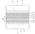
(成膜室の構成例)
本発明の一実施形態に係る成膜装置の主要な構成を図1及び図2に示す。図1は成膜装置の平面図であり、図中のA−B切断線に概略対応する断面図を図2に示す。以下の説明では図1及び図2の両図を参照して説明する。
(Configuration example of film formation chamber)
A main configuration of a film forming apparatus according to an embodiment of the present invention is shown in FIGS. FIG. 1 is a plan view of a film forming apparatus, and FIG. 2 shows a cross-sectional view roughly corresponding to the line AB in FIG. The following description will be given with reference to both FIGS.
成膜室104は、真空排気されて内部が減圧状態に保持される処理室102の中に設けられている。処理室102は処理室天板110と処理室底板112を含んで構成され、成膜室104は処理室天板110と処理室底板112の間に設けられている。成膜室104は、第1の蒸発源106及び第2の蒸発源108を防着板114で囲むようにして構成されている。
The
防着板114は中空構造を有している。防着板114の中空部分には加熱された流体が流れている。この流体は、一例としてシリコーンオイルなどが用いられる。
防着板114の中空部分に加熱された流体を流し、防着板114を蒸発源から放出される材料が付着しない温度まで加熱することで、該材料の利用効率を高めることができる。材料の利用効率とは、蒸発源から蒸発若しくは昇華した材料の全量に対する基板に付着して成膜される材料の割合である。
The
By flowing a heated fluid through the hollow portion of the
第1の蒸発源106は基板ホルダ116で保持された基板118と対向するように配置される。基板ホルダ116は搬送テーブル120に連結されている。第1の蒸発源106から放出される蒸気は基板118の全面に被着するものではなく、基板118の一部の領域に被着されるように配置されている。このような構成は、第2の蒸発源108についても同様である。
The
図1は第1の蒸発源106により形成される第1の成膜領域122を模式的に示す。同様に、第2の蒸発源108は第2の成膜領域124を形成する。第1の成膜領域122と第2の成膜領域124は必ずしも明確に区別されている必要はないが、第1の蒸発源106と第2の蒸発源108を離間して配置することで、それぞれの材料の蒸気が優先的に基板118に被着する領域が存在する。
成膜領域を明確に区別する場合には、第1の蒸発源106と第2の蒸発源108との間に遮蔽板を設けても良い。
FIG. 1 schematically shows a first
In the case of clearly distinguishing the film formation region, a shielding plate may be provided between the
第1の成膜領域122において、図1中にa−b線で示す基板118の中心から外周側に延びる線上の膜厚分布は一定になるようにすることが好ましい。そのために、成膜速度を考慮して、第1の蒸発源106及び第2の蒸発源108は、蒸気の放出口が基板118の中心側に向くように設けても良い。
In the first
基板118に所定の薄膜を形成するには、第1の蒸発源106及び第2の蒸発源108と基板118の一方又は双方を、駆動部126により相対的に移動させる。
例えば、蒸発源に対して基板を回転運動させる。その場合、駆動部126は、基板ホルダ116と回転軸128により連結されている。このようにすると、基板118のある一点では、第1の成膜領域122と第2の成膜領域124とが交互に出現することとなり、基板118の全面に薄膜を形成することが可能となる。
基板118の外周部はマスク115で遮蔽され成膜されないようにすることもできる。このマスク115の大きさは適宜変更することができる。
In order to form a predetermined thin film on the
For example, the substrate is rotated with respect to the evaporation source. In this case, the driving
The outer periphery of the
第1の蒸発源106と第2の蒸発源108への供給は同一の材料を供給しても良いし、異なる材料を供給しても良い。化合物の薄膜を基板118に形成する場合には、該化合物を構成する元素を、それぞれ異なる蒸発源に装填すれば良い。また、ホスト材料にゲスト材料を添加したい場合には、ホスト材料とゲスト材料を、それぞれの蒸発源に装填すれば良い。
なお、蒸発源は二つ以上設けても良く、その場合における蒸発源の構成は上記と同様である。
The same material may be supplied to the
Two or more evaporation sources may be provided, and the configuration of the evaporation source in that case is the same as described above.
上記構成の成膜装置に適用できる基板の形状は任意であるが、例えば円形(円盤型)の基板を適用するのは好ましい一態様となる。基板118を用いる場合には、中央部に貫通口が設けられているものを用いることができる。
その場合基板は中心軸で回転させ、蒸発源は中心軸から離れた位置に配置して回転運動する基板の一の領域に特定の成膜材料が被着されるように設ける。
The shape of the substrate applicable to the film formation apparatus having the above structure is arbitrary, but for example, it is a preferable aspect to apply a circular (disc-shaped) substrate. When the
In that case, the substrate is rotated about the central axis, and the evaporation source is arranged at a position away from the central axis so that a specific film forming material is deposited on one region of the substrate that rotates.
図3(A)に示すように、複数の蒸発源を異なる位置に配置することにより、薄膜130は複数の材料が混合した薄膜、又は複数の材料の層が格子状に配列した薄膜、若しくは複数の材料の単分子層(厚さ0.1nm〜10nm、代表的には0.5nm〜5nm)が膜厚方向に積層した薄膜であって、実質的に単分子超多層構造した薄膜を形成することが可能となる。
図3(B)で示すように、第1の電極132と第2の電極134の間に薄膜130が挟まれるように形成することで、このような繰り返し構造を貫通するように電流を流すことができる。
このように、基板を高速回転させつつ異なる材料を同時に成膜した場合、従来の共蒸着法とは異なるものとなる。
As shown in FIG. 3A, by arranging a plurality of evaporation sources at different positions, the
As shown in FIG. 3B, by forming the
Thus, when different materials are simultaneously formed while rotating the substrate at a high speed, the conventional co-evaporation method is different.
図4(A)はゲスト材料とホスト材料を共蒸着した場合の概念図を示す。共蒸着法では、ゲスト材料138とホスト材料136がうまく分散せず、領域Aとして示すように孤立するゲスト材料も存在すれば、領域Bとして示すように凝集するゲスト材料も存在する。それによりホスト材料も局所的に歪みが生じる。
一方、基板を高速回転させ、基板の一表面が蒸発源の上を通過する際に実質的に単分子若しくは数分子層が堆積されるようにすると、図4(B)で示すようにゲスト材料の配置は均等化され、凝集状態が生じるのを防ぐことができる。そして、領域Cとして示すようにゲスト材料の配置は均等化され、ホスト材料の中にゲスト材料を均等に含ませることが可能となる。
FIG. 4A shows a conceptual diagram when a guest material and a host material are co-evaporated. In the co-evaporation method, the
On the other hand, when the substrate is rotated at a high speed so that a single molecule or several molecular layers are substantially deposited when one surface of the substrate passes over the evaporation source, the guest material as shown in FIG. Can be equalized to prevent agglomeration. And as shown as the area | region C, arrangement | positioning of guest material is equalized and it becomes possible to make guest material contain evenly in host material.
基板の回転速度は、蒸発源から供給される単位時間当たりの成膜材料の量との関係で重要なパラメータとなる。ここで、一定の回転数で回転する円形基板は、円の外周と内周で線速度が異なるため、基板に被着する単位時間当たりの蒸着材料の量が円の外周と内周で同じ場合には、外周部で薄く内周部で厚く薄膜が形成されてしまう。そのため、円形基板の外周部に対して内周部に被着する成膜材料の量が少なくなるように、蒸発源を傾けて配設し、又は成膜材料の被着量を制御する遮蔽板を設けることが好ましい。
そして、被着する成膜材料が、実質的に単分子層が形成される速度で回転させることにより、上記のように複数の材料が均一に、または周期的に堆積された薄膜を得ることが可能である。回転数は300rpm(回転/分)から30000rprm、代表的には1000rpmが適用される。
The rotation speed of the substrate is an important parameter in relation to the amount of film forming material per unit time supplied from the evaporation source. Here, a circular substrate that rotates at a constant rotational speed has different linear velocities on the outer periphery and inner periphery of the circle, so the amount of vapor deposition material deposited on the substrate per unit time is the same on the outer periphery and inner periphery of the circle. In this case, a thin film is formed thinly at the outer peripheral portion and thick at the inner peripheral portion. Therefore, the shielding plate is arranged with the evaporation source tilted or the deposition amount of the film forming material is controlled so that the amount of the film forming material deposited on the inner periphery with respect to the outer periphery of the circular substrate is reduced. Is preferably provided.
Then, the film forming material to be deposited is rotated at a speed at which a monomolecular layer is substantially formed, thereby obtaining a thin film in which a plurality of materials are uniformly or periodically deposited as described above. Is possible. The number of rotations is 300 rpm (revolutions / minute) to 30000 rpm, typically 1000 rpm.
基板118の材質は、ガラス、セラミック、石英、プラスチックなど、様々なものを選択可能である。プラスチック材料では、ポリカーボネート、ポリアリレート、ポリエーテルスルフォン等を選択可能である。
As the material of the
基板118の大きさの一例は、CD−R等の光ディスクと同程度の大きさとすることができる。例えば、直径100mm〜140mm、一例として直径120mmの円盤形状であって、厚みを1.2〜1.5mm程度としたプラスチック基板を用いることができる。また、基板118に設ける貫通口の直径は、5mm〜20mm(例えば、15mm)とすることができる。
なお、基板118の形状は円形に限定されず、楕円状や矩形状としてもよい。
An example of the size of the
Note that the shape of the
(蒸発源の構成例)
図5に蒸発源の一例を示す。例示される第1の蒸発源106は、坩堝140と、坩堝140を加熱するヒータ142を有している。ヒータ142の一例は、ニクロム線など電気抵抗が高い導体で電路を形成し電流を通して発熱させるものである。なお、第2の蒸発源108も同様な構成とすることができる。
(Configuration example of evaporation source)
FIG. 5 shows an example of the evaporation source. The illustrated
第1の蒸発源106には、成膜に使用する材料の蒸発を間歇的に行うために、成膜する成膜材料144を坩堝140内に供給する材料供給部146が付加されていても良い。材料供給部146は、成膜する成膜材料144の装填部148と押出部150などにより構成される。
The
この場合、成膜材料144は1回の成膜処理(基板一枚当たり)に必要な量だけあれば良く、所定の形状に固められていることが好ましい。 In this case, the film forming material 144 may be in an amount necessary for one film forming process (per substrate), and is preferably solidified into a predetermined shape.
この成膜材料144を坩堝140内に供給する方法は任意である。例えば、装填部148を坩堝140に細管で連結し、細管を成膜材料144が通るように機械的に押し出す構成、又は気圧によって押し出す構成とすれば良い。気圧によって成膜材料144を押し出すにはアルゴンなどの不活性ガスを用い、ピエゾバルブなど0.5秒以内で開閉可能なバルブを使用してパルス的に圧縮した気体を送り込めば良い。
A method for supplying the film forming material 144 into the
このような材料供給部146があれば、基板毎に成膜材料144の供給が可能となり、成膜室に基板を出し入れする間は成膜材料144の蒸着を止めることができるので、成膜材料144の無駄を無くすことができる。
If such a
坩堝140の温度は蒸発若しくは昇華させる材料の無駄を無くすために、場所によって温度を異ならせておくことが好ましい。
成膜材料144が供給される坩堝140の底部の温度(T2)は、成膜材料144を急速に加熱して蒸気を発生させるために、成膜材料144が気化する温度以上に加熱する。坩堝140の先端(放出口)は、温度T2よりも低くて良いが、成膜材料144の蒸気が再付着してそこに堆積しない温度(T4)に加熱する。また、坩堝140の底部と先端部の間は、温度T2と温度T4の中間の温度(T3)とする。
坩堝140と装填部148の間を繋ぐ細管部も成膜材料144が気化しない温度(T1)で余熱しておくことは好ましい。
The temperature of the
The temperature (T2) at the bottom of the
It is preferable to preheat the narrow tube portion connecting the
このような第1の蒸発源106により、成膜材料144の蒸気の発生を制御することができるので、成膜材料144の無駄を省きつつ、連続して多数の基板に薄膜を形成することができる。
Since the
(成膜装置の構成例)
図6は複数の成膜室を有する成膜装置の一例を示す平面図である。成膜室は図1及び図2を参照して説明したものと同様な構成となっている。
(Configuration example of film deposition system)
FIG. 6 is a plan view showing an example of a film forming apparatus having a plurality of film forming chambers. The film forming chamber has the same configuration as that described with reference to FIGS.
この成膜装置100は、真空排気され減圧状態を保持することが可能な処理室102の中に配置される。処理室102の中には複数の膜室を設けることが可能であり、搬送テーブル120によって各成膜室に基板を搬送することにより、組成の異なる膜を連続して形成することができる。
The
基板搬出入室184は処理室102にゲートバルブを介して連結されている。基板搬出入室184は成膜前の基板を処理室102に搬入し、成膜処理の終わった基板を処理室102から回収する。
The substrate carry-in / out
図6においてC−D切断線に沿った断面構造の模式図を図7に示す。処理室102内に設けられる成膜室の構成は図1と同様である。処理室102は真空ポンプ186により真空排気される。この処理室102の中に複数の成膜室が配置されている。
FIG. 7 is a schematic diagram of a cross-sectional structure taken along the line CD in FIG. The structure of the film formation chamber provided in the
基板ホルダ116に保持された基板118は、搬送テーブル120によって、ある成膜室から他の成膜室に搬送される。基板ホルダ116は搬送テーブル120に連結されている。搬送テーブル120は搬送回転軸188によって搬送駆動部190に連結されており、搬送駆動部190が回動することによって処理室102内で基板118が搬送される。
The
(成膜装置の動作と照明装置の製造方法)
図6で示す成膜装置の動作について説明する。なお、本形態では、成膜装置を用いて図8に示す構成の照明装置192を製造する場合を例示する。図8は照明装置192の主要部を示す図である。この照明装置は、一対の電極間にエレクトロルミネセンス材料により構成される発光ユニットが、複数個積層された構造を有している。
(Operation of film forming apparatus and manufacturing method of lighting apparatus)
The operation of the film forming apparatus shown in FIG. 6 will be described. Note that in this embodiment, the case where the
照明装置192を形成するための基板118は、基板搬出入室184から予備室182を経て処理室102に搬入される。第1の成膜室152において第1絶縁膜198が形成される。第1絶縁膜198は酸化珪素、窒化珪素、窒化酸化珪素、酸化珪素を含む硫化亜鉛などの絶縁膜で形成する。第1絶縁膜198はエレクトロルミネセンス素子に水分が浸入するのを防ぐために設ける。特に基板118としてプラスチックなどの水蒸気透過率の高い材質のものを用いた場合に有効である。
A
第1絶縁膜198が形成された基板118を、第1の成膜室152から第2の成膜室154に搬送テーブル120を動作させて搬送する。この動作に伴って、基板搬出入室184から処理室102に新たな基板が搬入される。
第2の成膜室154において、第1絶縁膜198上に第1電極200が成膜される。第1電極200は、エレクトロルミネセンス素子の陽極又は陰極として用いられる電極である。
The
In the second
第1電極200を成膜後、基板118を第3の成膜室156へと搬送する。この動作に伴って、基板搬出入室184から処理室102に新たな基板が搬入され、第1の成膜室152にあった基板は、第2の成膜室154に移動する。以下、このような動作は連続して行われる。
After the
基板118は、第3の成膜室156から第5の成膜室160に移動する過程で、エレクトロルミネセンス素子により構成される第1の発光ユニット194が形成される。第1の発光ユニット194は正孔注入輸送層202、発光層204、電子注入輸送層206が積層されている。ここで、第3の成膜室156において正孔注入輸送層202が形成され、第4の成膜室158では発光層204が形成され、第5の成膜室160では電子注入輸送層206が形成される。
なお、第1の発光ユニット194の構成は少なくとも発光層204を有していれば、この構成に限定されない。処理室の構成を適宜変更することで第1の発光ユニット194の積層構造を変更することができる。
In the process of moving the
Note that the structure of the first light-emitting
第1の発光ユニット194が形成された基板118を第6の成膜室162へ搬送する。第6の成膜室162では、第1の発光ユニット194上に第1中間層208が形成される。第1中間層208は正孔輸送性の高い有機化合物と電子受容体(アクセプター)とを含む層として形成される。
The
第7の成膜室164では、第1中間層208上に第2中間層210が形成される。第2中間層210は電子輸送性の高い有機化合物と電子供与体(ドナー)とを含む層として形成される。
第1中間層208は第1発光ユニット194に電子を注入し、第2中間層210は第2の発光ユニット196に正孔を注入する。
なお、中間層の構成はこれに限られるものではなく、正孔輸送性の高い有機化合物と電子受容体(アクセプター)とを含む層、または、電子輸送性の高い有機化合物と電子供与体(ドナー)とを含む層の単層構造としてもよい。
In the seventh
The first
Note that the structure of the intermediate layer is not limited to this, and a layer containing an organic compound having a high hole-transport property and an electron acceptor (acceptor), or an organic compound having an electron-transport property and an electron donor (donor) ).
第2中間層210が形成された基板118は、第8の成膜室166から第11の成膜室172に移動する過程で、エレクトロルミネセンス素子で構成される第2の発光ユニット196が形成される。第2の発光ユニット196は正孔注入輸送層212、発光層214、電子輸送層216、電子注入層218が積層されている。
The
第8の成膜室166において、正孔注入輸送層212が形成され、第9の成膜室168では、発光層214が形成され第10の成膜室170では電子輸送層216が形成され、第11の成膜室172で電子注入層218が形成される。
In the eighth
第1の発光ユニット194から得られる発光の発光色と第2の発光ユニット196から得られる発光の発光色が補色の関係にある場合、外部へ取り出される光は白色発光となる。又は、第1の発光ユニット194及び第2の発光ユニット196のそれぞれが複数の発光層を有する構成として、複数層の発光層のそれぞれにおいて、互いに補色となる発光色を重ね合わせることによって各発光ユニットが白色発光を得られる構成としてもよい。補色の関係としては、青色と黄色、あるいは青緑色と赤色などがある。
When the light emission color obtained from the first
第2の発光ユニット196が形成された基板118を、第12の成膜室174へ搬送する。第12の成膜室174では、第2の発光ユニット196上に第2電極220が成膜される。
The
次いで、第2電極220が設けられた基板118を第13の成膜室176へ搬送する。第13の成膜室176において、第2電極220上に乾燥剤層222を設ける。
乾燥剤層222を形成することで、水分などによるエレクトロルミネセンス素子の劣化を防ぐことができる。乾燥剤としては、酸化カルシウムや酸化バリウム等のアルカリ土類金属の酸化物のような化学吸着によって水分を吸収する物質を用いることが可能である。その他の乾燥剤として、ゼオライトやシリカゲル等の物理吸着によって水分を吸着する物質を用いてもよい。
Next, the
By forming the
乾燥剤層222が設けられた基板118を第14の成膜室178へ搬送する。第14の成膜室178では、乾燥剤層222の上に第2絶縁膜224を形成する。第2絶縁膜224は、外部からの水分や不純物等がエレクトロルミネセンス素子へ侵入することを防止する。
The
第2絶縁膜224が設けられた基板118を第15の成膜室180へ搬送する。第15の成膜室180では、光硬化性又は熱硬化性のシール材226が設けられた封止基板228が封止基板搬出入室185から搬入され、基板118の第2絶縁膜224上に重ね合わされる。そして、シール材の硬化処理が施される。
封止基板228の材質は、ガラス、セラミック、石英、プラスチックなど、様々なものを選択可能である。プラスチック材料では、ポリカーボネート、ポリアリレート、ポリエーテルスルフォン等を選択可能である。
なお、封止基板228は必ずしも設ける必要はなく、エレクトロルミネセンス素子を封止膜によって封止した後、基板を成膜装置から搬出しても良い。
そして、基板118は予備室から基板搬出入室184に搬出される。
The
Various materials such as glass, ceramic, quartz, and plastic can be selected as the material of the sealing
Note that the sealing
Then, the
以上の工程によって、基板118を処理室102に搬入してから取り出すまで、大気に触れさせることなく連続して薄膜を積層し、照明装置192を製造することができる。
この成膜装置100を用いれば、ホスト材料中でゲスト材料が凝集することなく分散させることができ、発光効率の高い照明装置を製造することができる。
Through the above steps, the
By using this
(照明装置の一例)
図6の成膜装置で作製可能な照明装置の一例について図9及び図10を参照して説明する。図9は照明装置の平面図を示し、X1−X2切断線及びY1−Y2切断線に対応する断面構造を図10に示す。
(Example of lighting device)
An example of a lighting device that can be manufactured using the film formation apparatus in FIG. 6 will be described with reference to FIGS. FIG. 9 is a plan view of the lighting device, and FIG. 10 shows a cross-sectional structure corresponding to the X1-X2 cutting line and the Y1-Y2 cutting line.
照明装置192は、中央部に開口部230を有する基板118上に、第1絶縁膜198、第1電極200、発光ユニット232、第2電極220、乾燥剤層222、第2絶縁膜224が積層して設けられ、基板118の開口部230の近くに第1の接続部234及び第2の接続部236を有する。
In the
発光ユニット232は、図8で示すように第1の発光ユニット194と第2の発光ユニット196が積層されたタンデム型の構成とすると、発光輝度の電流効率を高めることができ、また、白色発光をすることが容易となるので好ましい。
When the
第2絶縁膜224は基板118の中央部において開口部を有しており、そこに第1の接続部234及び第2の接続部236が露出している。第1の接続部234は、第1電極200と電気的に接続されたものであり、実際には第1電極200が延伸されて第1の接続部234が構成されている。第2の接続部236は、第2電極220と電気的に接続されたものであり、実際には第2電極220が延伸されて第2の接続部236が構成されている。
The second
このように、基板118に形成された第1電極200及び第2電極220を引き出して、基板118に第1の接続部234及び第2の接続部236を形成することにより、照明装置192を薄型化することができる。
In this way, the
開口部230を有する基板118を用い、当該基板118の略中央部に第1の接続部234及び第2の接続部236を設けることにより、基板118の略中央部で照明装置192に給電することができる。基板118に開口部230が設けられていることにより、この部分を利用して基板118をソケットに固定することが容易となる。
By using the
照明装置192に接続部材238を設けた構成を図11に例示する。なお、接続部材238は口金又はソケットと呼ばれることもある。
接続部材238は、制御回路240と、第1の接続配線242、第2の接続配線244、第1の取り出し配線246及び第2の取り出し配線248を有している。
制御回路240は電源から供給される電源電圧を元に、照明装置192を点灯させるための機能を有する。
A structure in which the
The
The
接続部材238の第1の接続配線242は第1の接続部234と接続し、第2の接続配線244は、第2の接続部236と接続する。
第1の接続配線242と第1の接続部234との電気的な接続、第2の接続配線244と第2の接続部236との電気的な接続は、異方性導電性ペースト(ACP(Anisotropic Conductive Paste))、異方導電性フィルム(ACF(Anisotropic Conductive Film))、導電性ペースト、半田接合を用いて行うことができる。
第1の取り出し配線246、第2の取り出し配線248は、制御回路240と電気的に接続され、照明装置192へ電源を供給するための配線として機能する。
The
The electrical connection between the
The
図11(A)は、基板118が設けられた面から当該基板118を介して光を取り出す構成(ボトムエミッション構造)を示しており、この場合、接続部材238の制御回路240は、封止基板228の上方に設けた構成とすることができる。
FIG. 11A illustrates a structure (bottom emission structure) in which light is extracted from the surface provided with the
図11(B)は、封止基板228が設けられた面(基板118と反対側の面)側から光を取り出す構成(トップエミッション構造)としてもよい。この場合、基板118の裏面側に制御回路240が設けられ、基板118に設けられた開口部を介して第1の接続配線242及び第2の接続配線244が照明装置192と電気的に接続される構成となっている。
FIG. 11B may have a structure (top emission structure) in which light is extracted from the surface (surface opposite to the substrate 118) provided with the sealing
図11(A)、図11(B)では、接続部材238の勘合部が第1の取り出し配線246を兼ね、接続部材238の接点が第2の取り出し配線248に接続する構成であるが、図11(C)、図11(D)に示すように、接続部材238の二つの勘合部が第1の取り出し配線246と第2の取り出し配線248を兼ねる構成としてもよい。
11A and 11B, the fitting portion of the
次に、接続部材238が設けられた照明装置192の使用形態の一例を図12(A)、(B)に示す。図12(A)及び図12(B)は、照明装置192に取り付けられた接続部材238を、天井250に設ける場合を示している。
Next, an example of usage of the
天井250には、第1の外部電極252と第2の外部電極254が設けられており、当該第1の外部電極252と接続部材238に設けられた第1の取り出し配線246が電気的に接続し、且つ第2の外部電極254と第2の取り出し配線248が電気的に接続することにより、外部から制御回路240を介して照明装置192に電力が供給される。
The
図12(A)に示す構成において、接続部材238の直径は、天井250の取り付け部分のサイズに合わせて決めればよく、10mm〜40mm(例えば、26mm)とすることができる。
図12(A)は、図11(A)に示した構造を天井250に取り付け、図12(B)は、図11(C)に示した構造を天井250に取り付ける場合を示したが、これに限られず、他の構成も同様に取り付けることができる。また、天井250に限られず壁面や床に埋設することが可能である。
In the configuration illustrated in FIG. 12A, the diameter of the
12A shows the case where the structure shown in FIG. 11A is attached to the
100 成膜装置
102 処理室
104 成膜室
106 第1の蒸発源
108 第2の蒸発源
110 処理室天板
112 処理室底板
114 防着板
115 マスク
116 基板ホルダ
118 基板
120 搬送テーブル
122 第1の成膜領域
124 第2の成膜領域
126 駆動部
128 回転軸
130 薄膜
132 第1の電極
134 第2の電極
136 ゲスト材料
138 ホスト材料
140 坩堝
142 ヒータ
144 成膜材料
146 材料供給部
148 装填部
150 押出部
152 第1の成膜室
154 第2の成膜室
156 第3の成膜室
158 第4の成膜室
160 第5の成膜室
162 第6の成膜室
164 第7の成膜室
166 第8の成膜室
168 第9の成膜室
170 第10の成膜室
172 第11の成膜室
174 第12の成膜室
176 第13の成膜室
178 第14の成膜室
180 第15の成膜室
182 予備室
184 基板搬出入室
185 封止基板搬出入室
186 真空ポンプ
188 搬送回転軸
190 搬送駆動部
192 照明装置
194 第1の発光ユニット
196 第2の発光ユニット
198 第1絶縁膜
200 第1電極
202 正孔注入輸送層
204 発光層
206 電子注入輸送層
208 第1中間層
210 第2中間層
212 正孔注入輸送層
214 発光層
216 電子輸送層
218 電子注入層
220 第2電極
222 乾燥剤層
224 第2絶縁膜
226 シール材
228 封止基板
230 開口部
232 発光ユニット
234 第1の接続部
236 第2の接続部
238 接続部材
240 制御回路
242 第1の接続配線
244 第2の接続配線
246 第1の取り出し配線
248 第2の取り出し配線
250 天井
252 第1の外部電極
254 第2の外部電極
DESCRIPTION OF SYMBOLS 100 Film-forming apparatus 102 Processing chamber 104 Film-forming chamber 106 1st evaporation source 108 2nd evaporation source 110 Processing-chamber top plate 112 Processing-chamber bottom plate 114 Depositing plate 115 Mask 116 Substrate holder 118 Substrate 120 Transfer table 122 1st Film formation region 124 Second film formation region 126 Drive unit 128 Rotating shaft 130 Thin film 132 First electrode 134 Second electrode 136 Guest material 138 Host material 140 Crucible 142 Heater 144 Film formation material 146 Material supply unit 148 Loading unit 150 Extrusion unit 152 First film formation chamber 154 Second film formation chamber 156 Third film formation chamber 158 Fourth film formation chamber 160 Fifth film formation chamber 162 Sixth film formation chamber 164 Seventh film formation Chamber 166 Eighth film forming chamber 168 Ninth film forming chamber 170 Tenth film forming chamber 172 Eleventh film forming chamber 174 Twelfth film forming chamber 176 Thirteenth film forming chamber 178 No. 4 deposition chamber 180 Fifteenth deposition chamber 182 Preliminary chamber 184 Substrate carry-in / out chamber 185 Sealed substrate carry-in / out chamber 186 Vacuum pump 188 Transport rotary shaft 190 Transport drive unit 192 Illuminating device 194 First light emitting unit 196 Second light emission Unit 198 first insulating film 200 first electrode 202 hole injection transport layer 204 light emitting layer 206 electron injection transport layer 208 first intermediate layer 210 second intermediate layer 212 hole injection transport layer 214 light emitting layer 216 electron transport layer 218 electron injection Layer 220 second electrode 222 desiccant layer 224 second insulating film 226 sealing material 228 sealing substrate 230 opening 232 light-emitting unit 234 first connection portion 236 second connection portion 238 connection member 240 control circuit 242 first connection Wiring 244 Second connection wiring 246 First extraction wiring 248 Second extraction wiring 250 Ceiling 252 First external electrodes 254 second external electrode
Claims (1)
前記第1の成膜材料と前記第2の成膜材料が前記基板の被成膜面の全面に交互に被着するように前記基板を水平を保ちつつ回転させながら、前記被成膜面において前記第1の成膜材料と前記第2の成膜材料とが所定の比率で含まれるように共蒸着する成膜方法を用いて発光層を含む発光ユニットを形成する照明装置の作製方法であって、
前記第1の蒸発源および前記第2の蒸発源を傾け、
前記基板の回転数を300回転/分以上30000回転/分以下とし、
前記第1の蒸発源から前記第1の成膜材料としてホスト材料を供給し、前記第2の蒸発源から前記第2の成膜材料としてゲスト材料を供給することで前記ゲスト材料と前記ホスト材料を共蒸着することを特徴とする成膜方法を用いて発光層を含む発光ユニットを形成することを特徴とする照明装置の作製方法。 The first film-forming material is evaporated from a first evaporation source so that the first film-forming material is deposited on a partial region of the film-forming surface of the substrate, and the film-forming surface of the substrate Evaporating the second film-forming material from the second evaporation source so that the second film-forming material is deposited on the other part of the region,
While rotating the substrate while keeping the substrate horizontal so that the first film-forming material and the second film-forming material are alternately deposited on the entire film-forming surface of the substrate, A method for manufacturing a lighting device, wherein a light-emitting unit including a light-emitting layer is formed using a film-forming method in which the first film-forming material and the second film-forming material are co-evaporated so as to be included in a predetermined ratio. And
Tilting the first evaporation source and the second evaporation source;
The number of rotations of the substrate is set to 300 rpm / min to 30000 rpm,
The guest material and the host material are supplied by supplying a host material as the first film-forming material from the first evaporation source and supplying a guest material as the second film-forming material from the second evaporation source. A light-emitting unit including a light-emitting layer is formed using a film formation method characterized by co-evaporation of a light emitting device.
Priority Applications (1)
| Application Number | Priority Date | Filing Date | Title |
|---|---|---|---|
| JP2010071754A JP5417236B2 (en) | 2009-03-27 | 2010-03-26 | Method for manufacturing lighting device |
Applications Claiming Priority (3)
| Application Number | Priority Date | Filing Date | Title |
|---|---|---|---|
| JP2009080199 | 2009-03-27 | ||
| JP2009080199 | 2009-03-27 | ||
| JP2010071754A JP5417236B2 (en) | 2009-03-27 | 2010-03-26 | Method for manufacturing lighting device |
Publications (3)
| Publication Number | Publication Date |
|---|---|
| JP2010248629A JP2010248629A (en) | 2010-11-04 |
| JP2010248629A5 JP2010248629A5 (en) | 2013-02-14 |
| JP5417236B2 true JP5417236B2 (en) | 2014-02-12 |
Family
ID=42784563
Family Applications (1)
| Application Number | Title | Priority Date | Filing Date |
|---|---|---|---|
| JP2010071754A Expired - Fee Related JP5417236B2 (en) | 2009-03-27 | 2010-03-26 | Method for manufacturing lighting device |
Country Status (4)
| Country | Link |
|---|---|
| US (1) | US20100247747A1 (en) |
| JP (1) | JP5417236B2 (en) |
| KR (1) | KR20100108283A (en) |
| TW (1) | TWI532861B (en) |
Families Citing this family (17)
| Publication number | Priority date | Publication date | Assignee | Title |
|---|---|---|---|---|
| JP5715802B2 (en) * | 2010-11-19 | 2015-05-13 | 株式会社半導体エネルギー研究所 | Deposition equipment |
| JP5852855B2 (en) * | 2010-11-24 | 2016-02-03 | 株式会社半導体エネルギー研究所 | LIGHT EMITTING ELEMENT, LIGHT EMITTING DEVICE, LIGHTING DEVICE, AND ELECTRONIC DEVICE |
| KR101218346B1 (en) * | 2011-02-09 | 2013-01-21 | 서울대학교산학협력단 | Method for formation of small molecule thin film and small molecule organic solar cell including bulk heterojunction |
| KR20140004761A (en) * | 2011-03-18 | 2014-01-13 | 도쿄엘렉트론가부시키가이샤 | Film forming apparatus, film forming method, method for manufacturing organic light emitting element, and organic light emitting element |
| CN103871851B (en) * | 2012-12-18 | 2017-12-19 | 北京创昱科技有限公司 | A kind of arrangement of copper indium gallium selenide film battery coevaporation linear sources array |
| CN103305794B (en) * | 2013-06-09 | 2016-03-02 | 京东方科技集团股份有限公司 | A kind of organic film plating device and method |
| US9209422B2 (en) * | 2013-12-31 | 2015-12-08 | Lg Display Co., Ltd. | Organic light emitting display device with micro-cavity structure |
| JP6627620B2 (en) * | 2016-04-05 | 2020-01-08 | 株式会社オートネットワーク技術研究所 | Connectors, connection status detection systems, and terminals |
| KR102353663B1 (en) | 2016-05-20 | 2022-01-19 | 가부시키가이샤 한도오따이 에네루기 켄큐쇼 | Light-emitting element, light-emitting device, electronic device, and lighting device |
| KR20180002505A (en) | 2016-06-29 | 2018-01-08 | 가부시키가이샤 한도오따이 에네루기 켄큐쇼 | Manufacturing method of light-emitting element |
| CN107799658B (en) | 2016-08-29 | 2021-05-28 | 株式会社半导体能源研究所 | Light-emitting element, light-emitting device, electronic device, lighting device, and organometallic complex |
| WO2018184949A1 (en) * | 2017-04-07 | 2018-10-11 | Applied Materials, Inc. | Method for cleaning a vacuum chamber, apparatus for vacuum processing of a substrate, and system for the manufacture of devices having organic materials |
| CN108728801B (en) * | 2018-05-28 | 2019-11-12 | 深圳市华星光电技术有限公司 | Evaporation coating device and evaporation coating method |
| GB2574400B (en) | 2018-06-04 | 2022-11-23 | Dyson Technology Ltd | A Device |
| GB2574401B (en) * | 2018-06-04 | 2022-11-23 | Dyson Technology Ltd | A Device |
| KR20210008427A (en) * | 2018-06-07 | 2021-01-21 | 실라나 유브이 테크놀로지스 피티이 리미티드 | Method and material deposition system for semiconductor layer formation |
| WO2024030562A1 (en) * | 2022-08-04 | 2024-02-08 | Emagin Corporation | Evaporation system having improved collimation |
Family Cites Families (36)
| Publication number | Priority date | Publication date | Assignee | Title |
|---|---|---|---|---|
| US4681773A (en) * | 1981-03-27 | 1987-07-21 | American Telephone And Telegraph Company At&T Bell Laboratories | Apparatus for simultaneous molecular beam deposition on a plurality of substrates |
| JPS63274756A (en) * | 1987-04-28 | 1988-11-11 | Toda Kogyo Corp | Vapor deposited multi-layered thin film forming device |
| FR2733253B1 (en) * | 1995-04-24 | 1997-06-13 | Commissariat Energie Atomique | DEVICE FOR DEPOSITING MATERIAL BY EVAPORATION ON LARGE SURFACE SUBSTRATES |
| GB9515929D0 (en) * | 1995-08-03 | 1995-10-04 | Fisons Plc | Sources used in molecular beam epitaxy |
| CH692000A5 (en) * | 1995-11-13 | 2001-12-31 | Unaxis Balzers Ag | Coating chamber, substrate carrier therefor, method of vacuum deposition and coating methods. |
| TW387152B (en) * | 1996-07-24 | 2000-04-11 | Tdk Corp | Solar battery and manufacturing method thereof |
| US6053981A (en) * | 1998-09-15 | 2000-04-25 | Coherent, Inc. | Effusion cell and method of use in molecular beam epitaxy |
| JP4469430B2 (en) * | 1998-11-30 | 2010-05-26 | 株式会社アルバック | Vapor deposition equipment |
| JP2001209981A (en) * | 1999-02-09 | 2001-08-03 | Ricoh Co Ltd | Device and method for forming optical disk substrate film, manufacturing method for substrate holder, substrate holder, optical disk and phase change recording optical disk |
| JP2001081558A (en) * | 1999-09-13 | 2001-03-27 | Asahi Optical Co Ltd | Film deposition device and film deposition method |
| US6082296A (en) * | 1999-09-22 | 2000-07-04 | Xerox Corporation | Thin film deposition chamber |
| JP4268303B2 (en) * | 2000-02-01 | 2009-05-27 | キヤノンアネルバ株式会社 | Inline type substrate processing equipment |
| US20020069970A1 (en) * | 2000-03-07 | 2002-06-13 | Applied Materials, Inc. | Temperature controlled semiconductor processing chamber liner |
| US20020011205A1 (en) * | 2000-05-02 | 2002-01-31 | Shunpei Yamazaki | Film-forming apparatus, method of cleaning the same, and method of manufacturing a light-emitting device |
| ATE497028T1 (en) * | 2000-06-22 | 2011-02-15 | Panasonic Elec Works Co Ltd | DEVICE AND METHOD FOR VACUUM EVAPORATION |
| JP2002071944A (en) * | 2000-08-24 | 2002-03-12 | Toyo Commun Equip Co Ltd | Apparatus and method for manufacturing optical band pass filter |
| JP2003193217A (en) * | 2001-12-25 | 2003-07-09 | Nippon Seiki Co Ltd | Vapor deposition apparatus |
| KR100467805B1 (en) * | 2002-01-22 | 2005-01-24 | 학교법인연세대학교 | Linear or planar type evaporator for the controllable film thickness profile |
| US6771021B2 (en) * | 2002-05-28 | 2004-08-03 | Eastman Kodak Company | Lighting apparatus with flexible OLED area illumination light source and fixture |
| US6787990B2 (en) * | 2002-05-28 | 2004-09-07 | Eastman Kodak Company | OLED area illumination light source having flexible substrate on a support |
| US6565231B1 (en) * | 2002-05-28 | 2003-05-20 | Eastman Kodak Company | OLED area illumination lighting apparatus |
| TWI277363B (en) * | 2002-08-30 | 2007-03-21 | Semiconductor Energy Lab | Fabrication system, light-emitting device and fabricating method of organic compound-containing layer |
| KR100889758B1 (en) * | 2002-09-03 | 2009-03-20 | 삼성모바일디스플레이주식회사 | Heating crucible of organic thin film forming apparatus |
| DE10316228B3 (en) * | 2003-04-09 | 2004-12-16 | Dr. Eberl Mbe-Komponenten Gmbh | Effusion cell with improved crucible temperature control |
| US7339139B2 (en) * | 2003-10-03 | 2008-03-04 | Darly Custom Technology, Inc. | Multi-layered radiant thermal evaporator and method of use |
| US7439208B2 (en) * | 2003-12-01 | 2008-10-21 | Superconductor Technologies, Inc. | Growth of in-situ thin films by reactive evaporation |
| US20050229856A1 (en) * | 2004-04-20 | 2005-10-20 | Malik Roger J | Means and method for a liquid metal evaporation source with integral level sensor and external reservoir |
| JP4653418B2 (en) * | 2004-05-17 | 2011-03-16 | 芝浦メカトロニクス株式会社 | Vacuum processing apparatus and optical disc manufacturing method |
| JP4027914B2 (en) * | 2004-05-21 | 2007-12-26 | 株式会社半導体エネルギー研究所 | LIGHTING DEVICE AND DEVICE USING THE SAME |
| JP2006002200A (en) * | 2004-06-16 | 2006-01-05 | Seiko Epson Corp | Vapor deposition apparatus, vapor deposition method, organic el apparatus, and electronic equipment |
| US7667389B2 (en) * | 2004-12-06 | 2010-02-23 | Semiconductor Energy Laboratory Co., Ltd. | Light emitting element, light emitting device, and electronic device |
| US20060244373A1 (en) * | 2005-04-28 | 2006-11-02 | Semiconductor Energy Laboratory Co., Ltd. | Light emitting device and method for manufacturing thereof |
| JP2008108611A (en) * | 2006-10-26 | 2008-05-08 | Fuji Electric Holdings Co Ltd | Forming method and forming apparatus of evaporation layer |
| JP4293314B2 (en) * | 2007-01-26 | 2009-07-08 | 財団法人山形県産業技術振興機構 | Lighting device |
| US8444926B2 (en) * | 2007-01-30 | 2013-05-21 | Applied Materials, Inc. | Processing chamber with heated chamber liner |
| US20090020070A1 (en) * | 2007-07-19 | 2009-01-22 | Michael Schafer | Vacuum evaporation apparatus for solid materials |
-
2010
- 2010-03-23 US US12/729,881 patent/US20100247747A1/en not_active Abandoned
- 2010-03-24 TW TW099108714A patent/TWI532861B/en not_active IP Right Cessation
- 2010-03-26 JP JP2010071754A patent/JP5417236B2/en not_active Expired - Fee Related
- 2010-03-26 KR KR1020100027140A patent/KR20100108283A/en active Search and Examination
Also Published As
| Publication number | Publication date |
|---|---|
| JP2010248629A (en) | 2010-11-04 |
| TWI532861B (en) | 2016-05-11 |
| TW201102447A (en) | 2011-01-16 |
| US20100247747A1 (en) | 2010-09-30 |
| KR20100108283A (en) | 2010-10-06 |
Similar Documents
| Publication | Publication Date | Title |
|---|---|---|
| JP5417236B2 (en) | Method for manufacturing lighting device | |
| JP4455937B2 (en) | Deposition source, vacuum film formation apparatus, organic EL panel manufacturing method | |
| KR101457653B1 (en) | Film formation apparatus, manufacturing apparatus, film formation method, and method for manufacturing a light-emitting device | |
| TW200844246A (en) | Film formation apparatus, film formation method, manufacturing apparatus, and method for manufacturing light-emitting device | |
| JP5166942B2 (en) | Method for manufacturing light emitting device | |
| JP2006057173A (en) | Film deposition source, vacuum film deposition apparatus and method for producing organic el panel | |
| JP4881789B2 (en) | Organic electroluminescence device manufacturing method and organic electroluminescence device manufacturing apparatus | |
| JP5325471B2 (en) | Method for manufacturing light emitting device | |
| CN1766157A (en) | Apparatus for fabricating display device | |
| US9290842B2 (en) | Electrode cover and evaporation device | |
| TWI516622B (en) | Device for evaporation | |
| JP2009114517A (en) | Vapor deposition apparatus, vapor deposition method, and method of manufacturing organic el apparatus | |
| JP5798452B2 (en) | Evaporation source | |
| JPH09256142A (en) | Film forming device | |
| JP4846650B2 (en) | Electrode cover and vapor deposition device | |
| JP2004204289A (en) | Apparatus and method for forming film, and apparatus and method for manufacturing display panel | |
| JP6271241B2 (en) | Vapor deposition apparatus and organic EL device manufacturing method | |
| JP2007095545A (en) | Method and apparatus of manufacturing self-luminescent element | |
| JP2006002218A (en) | Film-forming source, film-forming method, hot plate, and method for manufacturing organic el element | |
| JP2012111977A (en) | Film deposition apparatus and film deposition method, and method for manufacturing illumination device | |
| JP5839556B2 (en) | Deposition method | |
| JP2009206008A (en) | Method of manufacturing light-emitting device and manufacturing device used for the same | |
| JP2001057289A (en) | Manufacturing device for organic el display device and manufacture thereof | |
| WO2012108363A1 (en) | Crucible, vapor deposition apparatus, vapor deposition method, and method for manufacturing organic electroluminescent display device | |
| JP2004055452A (en) | Manufacturing method of organic light emitting device |
Legal Events
| Date | Code | Title | Description |
|---|---|---|---|
| A521 | Request for written amendment filed |
Free format text: JAPANESE INTERMEDIATE CODE: A523 Effective date: 20121224 |
|
| A621 | Written request for application examination |
Free format text: JAPANESE INTERMEDIATE CODE: A621 Effective date: 20121224 |
|
| A977 | Report on retrieval |
Free format text: JAPANESE INTERMEDIATE CODE: A971007 Effective date: 20130925 |
|
| A131 | Notification of reasons for refusal |
Free format text: JAPANESE INTERMEDIATE CODE: A131 Effective date: 20131015 |
|
| A521 | Request for written amendment filed |
Free format text: JAPANESE INTERMEDIATE CODE: A523 Effective date: 20131022 |
|
| TRDD | Decision of grant or rejection written | ||
| A01 | Written decision to grant a patent or to grant a registration (utility model) |
Free format text: JAPANESE INTERMEDIATE CODE: A01 Effective date: 20131112 |
|
| A61 | First payment of annual fees (during grant procedure) |
Free format text: JAPANESE INTERMEDIATE CODE: A61 Effective date: 20131118 |
|
| R150 | Certificate of patent or registration of utility model |
Ref document number: 5417236 Country of ref document: JP Free format text: JAPANESE INTERMEDIATE CODE: R150 Free format text: JAPANESE INTERMEDIATE CODE: R150 |
|
| R250 | Receipt of annual fees |
Free format text: JAPANESE INTERMEDIATE CODE: R250 |
|
| R250 | Receipt of annual fees |
Free format text: JAPANESE INTERMEDIATE CODE: R250 |
|
| R250 | Receipt of annual fees |
Free format text: JAPANESE INTERMEDIATE CODE: R250 |
|
| LAPS | Cancellation because of no payment of annual fees |