JP5409315B2 - Display device - Google Patents
Display device Download PDFInfo
- Publication number
- JP5409315B2 JP5409315B2 JP2009282284A JP2009282284A JP5409315B2 JP 5409315 B2 JP5409315 B2 JP 5409315B2 JP 2009282284 A JP2009282284 A JP 2009282284A JP 2009282284 A JP2009282284 A JP 2009282284A JP 5409315 B2 JP5409315 B2 JP 5409315B2
- Authority
- JP
- Japan
- Prior art keywords
- protective film
- organic
- organic protective
- forming
- display device
- Prior art date
- Legal status (The legal status is an assumption and is not a legal conclusion. Google has not performed a legal analysis and makes no representation as to the accuracy of the status listed.)
- Expired - Fee Related
Links
- 230000001681 protective effect Effects 0.000 claims description 141
- 239000000463 material Substances 0.000 claims description 55
- 238000000034 method Methods 0.000 claims description 47
- 239000000758 substrate Substances 0.000 claims description 30
- 150000002894 organic compounds Chemical class 0.000 claims description 13
- 238000004519 manufacturing process Methods 0.000 claims description 12
- 229910010272 inorganic material Inorganic materials 0.000 claims description 10
- 239000011147 inorganic material Substances 0.000 claims description 10
- 230000002093 peripheral effect Effects 0.000 claims description 8
- 238000000206 photolithography Methods 0.000 claims description 7
- 239000002689 soil Substances 0.000 claims 1
- 239000010408 film Substances 0.000 description 202
- 230000008569 process Effects 0.000 description 25
- 230000015572 biosynthetic process Effects 0.000 description 11
- 239000003822 epoxy resin Substances 0.000 description 9
- 229920000647 polyepoxide Polymers 0.000 description 9
- XLOMVQKBTHCTTD-UHFFFAOYSA-N Zinc monoxide Chemical compound [Zn]=O XLOMVQKBTHCTTD-UHFFFAOYSA-N 0.000 description 8
- 238000010438 heat treatment Methods 0.000 description 7
- 238000007789 sealing Methods 0.000 description 6
- 239000000203 mixture Substances 0.000 description 5
- 238000004544 sputter deposition Methods 0.000 description 5
- 238000010586 diagram Methods 0.000 description 4
- 229910003437 indium oxide Inorganic materials 0.000 description 4
- PJXISJQVUVHSOJ-UHFFFAOYSA-N indium(iii) oxide Chemical compound [O-2].[O-2].[O-2].[In+3].[In+3] PJXISJQVUVHSOJ-UHFFFAOYSA-N 0.000 description 4
- 238000000059 patterning Methods 0.000 description 4
- 239000011787 zinc oxide Substances 0.000 description 4
- 230000009471 action Effects 0.000 description 3
- QVGXLLKOCUKJST-UHFFFAOYSA-N atomic oxygen Chemical compound [O] QVGXLLKOCUKJST-UHFFFAOYSA-N 0.000 description 3
- 238000000576 coating method Methods 0.000 description 3
- 238000007796 conventional method Methods 0.000 description 3
- 239000007789 gas Substances 0.000 description 3
- 239000011521 glass Substances 0.000 description 3
- 150000007529 inorganic bases Chemical class 0.000 description 3
- 239000001301 oxygen Substances 0.000 description 3
- 229910052760 oxygen Inorganic materials 0.000 description 3
- 229920001721 polyimide Polymers 0.000 description 3
- 239000009719 polyimide resin Substances 0.000 description 3
- 238000007639 printing Methods 0.000 description 3
- 238000007650 screen-printing Methods 0.000 description 3
- 229920001187 thermosetting polymer Polymers 0.000 description 3
- 238000007740 vapor deposition Methods 0.000 description 3
- 230000000903 blocking effect Effects 0.000 description 2
- 239000012299 nitrogen atmosphere Substances 0.000 description 2
- 239000011368 organic material Substances 0.000 description 2
- 238000005268 plasma chemical vapour deposition Methods 0.000 description 2
- 229920005989 resin Polymers 0.000 description 2
- 239000011347 resin Substances 0.000 description 2
- 230000007480 spreading Effects 0.000 description 2
- 238000003892 spreading Methods 0.000 description 2
- 239000004925 Acrylic resin Substances 0.000 description 1
- 229920000178 Acrylic resin Polymers 0.000 description 1
- 229910052581 Si3N4 Inorganic materials 0.000 description 1
- 239000012298 atmosphere Substances 0.000 description 1
- 230000005540 biological transmission Effects 0.000 description 1
- 230000015556 catabolic process Effects 0.000 description 1
- 238000005229 chemical vapour deposition Methods 0.000 description 1
- 239000011248 coating agent Substances 0.000 description 1
- 239000004020 conductor Substances 0.000 description 1
- 230000003247 decreasing effect Effects 0.000 description 1
- 230000002950 deficient Effects 0.000 description 1
- 238000006731 degradation reaction Methods 0.000 description 1
- 230000006866 deterioration Effects 0.000 description 1
- 238000001035 drying Methods 0.000 description 1
- 230000000694 effects Effects 0.000 description 1
- 239000000839 emulsion Substances 0.000 description 1
- 238000005530 etching Methods 0.000 description 1
- 230000005525 hole transport Effects 0.000 description 1
- 238000002347 injection Methods 0.000 description 1
- 239000007924 injection Substances 0.000 description 1
- 230000007246 mechanism Effects 0.000 description 1
- 230000003287 optical effect Effects 0.000 description 1
- 229920002120 photoresistant polymer Polymers 0.000 description 1
- 230000009467 reduction Effects 0.000 description 1
- HQVNEWCFYHHQES-UHFFFAOYSA-N silicon nitride Chemical compound N12[Si]34N5[Si]62N3[Si]51N64 HQVNEWCFYHHQES-UHFFFAOYSA-N 0.000 description 1
- 238000009751 slip forming Methods 0.000 description 1
- 239000010409 thin film Substances 0.000 description 1
- 238000009281 ultraviolet germicidal irradiation Methods 0.000 description 1
- XLYOFNOQVPJJNP-UHFFFAOYSA-N water Substances O XLYOFNOQVPJJNP-UHFFFAOYSA-N 0.000 description 1
- 239000013585 weight reducing agent Substances 0.000 description 1
Images


Classifications
-
- H—ELECTRICITY
- H10—SEMICONDUCTOR DEVICES; ELECTRIC SOLID-STATE DEVICES NOT OTHERWISE PROVIDED FOR
- H10K—ORGANIC ELECTRIC SOLID-STATE DEVICES
- H10K59/00—Integrated devices, or assemblies of multiple devices, comprising at least one organic light-emitting element covered by group H10K50/00
- H10K59/80—Constructional details
- H10K59/87—Passivation; Containers; Encapsulations
- H10K59/873—Encapsulations
-
- H—ELECTRICITY
- H10—SEMICONDUCTOR DEVICES; ELECTRIC SOLID-STATE DEVICES NOT OTHERWISE PROVIDED FOR
- H10K—ORGANIC ELECTRIC SOLID-STATE DEVICES
- H10K50/00—Organic light-emitting devices
- H10K50/80—Constructional details
- H10K50/84—Passivation; Containers; Encapsulations
- H10K50/844—Encapsulations
-
- H—ELECTRICITY
- H10—SEMICONDUCTOR DEVICES; ELECTRIC SOLID-STATE DEVICES NOT OTHERWISE PROVIDED FOR
- H10K—ORGANIC ELECTRIC SOLID-STATE DEVICES
- H10K59/00—Integrated devices, or assemblies of multiple devices, comprising at least one organic light-emitting element covered by group H10K50/00
- H10K59/80—Constructional details
- H10K59/87—Passivation; Containers; Encapsulations
- H10K59/871—Self-supporting sealing arrangements
- H10K59/8723—Vertical spacers, e.g. arranged between the sealing arrangement and the OLED
Landscapes
- Physics & Mathematics (AREA)
- Optics & Photonics (AREA)
- Electroluminescent Light Sources (AREA)
- Devices For Indicating Variable Information By Combining Individual Elements (AREA)
Description
本発明は、有機保護膜と無機保護膜とによって封止された表示装置に関する。 The present invention relates to a display device sealed with an organic protective film and an inorganic protective film.
近年、薄型かつ軽量な表示装置として、自発光型の有機発光素子を用いた表示装置が注目されている。有機発光素子を用いた表示装置にとって、水分や酸素に対する耐久性は重要な課題の一つである。表示装置に水分や酸素が侵入すると、有機発光素子を構成する有機化合物層材料が劣化し、表示装置にはダークスポットと呼ばれる非発光領域が発生して表示性能が低下してしまう。 In recent years, a display device using a self-luminous organic light emitting element has attracted attention as a thin and lightweight display device. For display devices using organic light-emitting elements, durability against moisture and oxygen is one of the important issues. When moisture or oxygen enters the display device, the organic compound layer material constituting the organic light-emitting element is deteriorated, and a non-light-emitting region called a dark spot is generated in the display device, so that display performance is deteriorated.
表示装置の水分や酸素に対する耐久性を改善する手段として、有機保護膜と無機保護膜とを積層した封止構成が知られている。この封止構成において、水分等の侵入は無機保護膜によって抑制されるが、有機保護膜はこの無機保護膜に欠陥が生じないように、表示装置表面の凹凸を平坦化するために設けられている。そこで、有機保護膜は少なくとも有機発光素子が設けられた領域を覆うように形成され、無機保護膜は有機保護膜を覆い、有機保護膜の周囲で有機発光素子よりも下にある無機材料からなる部材と接するように、有機保護膜よりも広い領域に形成される。これにより、有機保護膜表面、周囲、および、発光素子の下側からの水分の浸入を防止することが可能となる。 As a means for improving durability against moisture and oxygen of a display device, a sealing configuration in which an organic protective film and an inorganic protective film are laminated is known. In this sealing configuration, intrusion of moisture or the like is suppressed by the inorganic protective film, but the organic protective film is provided to flatten the unevenness of the surface of the display device so that the inorganic protective film is not defective. Yes. Therefore, the organic protective film is formed so as to cover at least a region where the organic light emitting element is provided, and the inorganic protective film covers the organic protective film, and is made of an inorganic material below the organic light emitting element around the organic protective film. It is formed in a wider area than the organic protective film so as to be in contact with the member. Accordingly, it is possible to prevent moisture from entering from the surface of the organic protective film, the periphery, and the lower side of the light emitting element.
特許文献1は、有機保護膜(緩衝層)をウェットプロセス(塗布工程)で形成する技術に関するもので、有機保護膜材料が所定領域より外に流れ出さないよう堰き止めるための枠部を有する表示装置が記載されている。これにより、必要な領域にのみ有機保護膜材料を形成することができ、有機保護膜の周囲で無機保護膜と有機発光素子よりも下にある無機材料からなる部材とが接する領域を確保することが可能となる。
ディスペンス法や印刷法などのウェットプロセスによる膜形成法は、真空装置を用いたドライプロセスによる膜形成法よりも低コストであるため好ましいが、次のような課題がある。 A film forming method by a wet process such as a dispensing method or a printing method is preferable because it is less expensive than a film forming method by a dry process using a vacuum apparatus, but has the following problems.
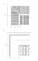
図8は、有機保護膜10と無機保護膜11との積層によって封止された表示装置端部の断面模式図である。有機保護膜10は表示領域Aを覆うように形成され、無機保護膜11は有機保護膜10を覆い、かつ、有機保護膜10の周囲で支持基板1と接するように、有機保護膜よりも広い領域に形成されている。ここでは、支持基板1が無機材料から構成されているとする。
FIG. 8 is a schematic cross-sectional view of the end portion of the display device sealed by stacking the organic
ウェットプロセスで有機保護膜10を形成した場合、有機保護膜材料の粘性や支持基板1に対する濡れ性に応じて、端部には傾斜部Bができる。例えば、表示領域Aから傾斜部Bの幅bだけ外側の位置Eに有機保護膜の端部形成位置を設定する場合を考える。ウェットプロセスの成膜位置精度には、誤差±mが含まれるため、有機保護膜10の端部は、位置Eから表示領域側にmずれた位置Fと、反対側にmずれた位置Gとの間の不確定な位置に形成されることになる。もし、有機保護膜10の端部が位置Fに形成されると、有機保護膜10の傾斜部Bが表示領域Aに掛かってしまい、外光反射が傾斜部Bで局所的に歪んで画像劣化が生じてしまう。従って、傾斜部Bが表示領域Aに掛からないように、有機保護膜10を形成しなければならない。
When the organic
そこで、有機保護膜材料の端部形成位置を位置Eからmだけ表示領域から離れた位置Gに設定し、有機保護膜10の端部がプロセスの誤差によって最も表示領域側にずれた場合でも、位置Eで留まるように形成することが考えられる。このとき、表示領域の外側(額縁領域)に必要な幅dは、次式で表される。
d≧b+2m+c ・・・(1)
cは、有機保護膜10の周囲で、無機保護膜11と有機発光素子よりも下にある無機材料からなる部材とが接するのに必要な幅を表している。式(1)からわかるように、ウェットプロセスの誤差±mを考慮して、額縁領域に必要な最小幅b+cに加えて余分な幅が2m必要となっていることがわかる。
Therefore, even when the edge forming position of the organic protective film material is set to a position G away from the display area by m from the position E, even when the edge of the organic
d ≧ b + 2m + c (1)
c represents a width necessary for the inorganic
特許文献1は、枠部を設け、流動性の高い有機保護膜材料を塗布することにより、所定領域外への有機保護膜材料の流出を防止し、有機保護膜の端部を所定領域に確実に形成することを可能にしている。そのため、有機保護膜材料の塗布時には、誤差mを考慮する必要がない。しかし、流動性の高い材料で表示装置表面の凹凸を平坦化するのに十分な膜厚の有機保護膜を形成するには、枠部を膜厚に相当する高さに設ける必要がある。特許文献1には、高粘度の材料をディスペンサ或いはスクリーン印刷で枠部を所定位置に設けると記載されている。つまり、枠部を設ける工程でウェットプロセスの誤差2mが額縁領域に必要となり、従来と同様の問題が生じる。さらに、枠部まで有機保護膜材料を広がらせるためには、用いる材料が1〜30cp程度の粘度でなければならず、有機保護膜に適用可能な材料が制限されるという問題も生じる。
In
有機光素子を用いた表示装置は、薄型化および軽量化が可能であるため、モバイル機器のディスプレイに用いられることが多い。モバイル機器のディスプレイにおいては、薄型化および軽量化に加えて、額縁領域の幅が狭いこと、すなわち狭額縁化と、低コスト化は大きな課題となっており、特許文献1の技術では、まだ狭額縁化が十分とは言えない。 Since a display device using an organic optical element can be thinned and lightened, it is often used for a display of a mobile device. In mobile device displays, in addition to thinning and weight reduction, the width of the frame region is narrow, that is, the narrowing of the frame and the cost reduction are major issues. The frame is not enough.
上記問題を解決するため、本発明にかかる有機発光表示装置は、
基板と、
前記基板上に複数の発光素子が配置された表示領域と、
少なくとも前記表示領域を覆う有機保護膜と、
前記有機保護膜を覆う無機保護膜と、
を備える表示装置であって、
前記表示領域の外周に沿って、前記表示領域の外周と交差する方向に、複数の溝が設けられた領域と、
前記溝が設けられた領域の外周に溝の設けられていない領域と、
を有することを特徴とする。
In order to solve the above problem, an organic light-emitting display device according to the present invention includes:
A substrate,
A display area in which a plurality of light emitting elements are disposed on the substrate;
An organic protective film covering at least the display area;
An inorganic protective film covering the organic protective film;
A display device comprising:
A region provided with a plurality of grooves in a direction intersecting the outer periphery of the display region along the outer periphery of the display region;
A region where no groove is provided on the outer periphery of the region where the groove is provided; and
It is characterized by having.
また、本発明に係る表示装置の製造方法は、
基板に複数の発光素子が配置された表示領域を形成する工程と、
前記表示領域の外周に沿って、前記表示領域の辺と交差する方向に、所定位置まで、複数の溝を設ける工程と、
前記表示領域を覆う有機保護膜を形成する工程と、
前記有機保護膜を覆う無機保護膜を形成する工程と、
を有する表示装置の製造方法であって、
前記有機保護膜を形成する工程は、有機保護膜材料を塗布して形成する工程であって、
前記有機保護膜材料の端部を前記溝の上に配置するように塗布する工程と、
前記有機保護膜材料を前記所定位置まで広げる工程と、
を有していることを特徴とする。
In addition, a method for manufacturing a display device according to the present invention includes:
Forming a display region in which a plurality of light emitting elements are arranged on a substrate;
Providing a plurality of grooves up to a predetermined position in a direction intersecting the side of the display area along the outer periphery of the display area;
Forming an organic protective film covering the display area;
Forming an inorganic protective film covering the organic protective film;
A method of manufacturing a display device having
The step of forming the organic protective film is a step of applying and forming an organic protective film material,
Applying an end of the organic protective film material so as to be disposed on the groove;
Expanding the organic protective film material to the predetermined position;
It is characterized by having.
本発明の表示装置によれば、有機保護膜の形成位置がウェットプロセスの誤差分ずれても、溝によって有機保護膜材料を広げ、有機保護膜材料を所定位置まで再現性良く塗布することが可能となる。その結果、プロセスマージンを低減することができ、額縁領域の狭い表示装置を低コストで製造することが可能となる。 According to the display device of the present invention, it is possible to spread the organic protective film material by the groove and apply the organic protective film material to a predetermined position with good reproducibility even if the formation position of the organic protective film is shifted by the wet process error. It becomes. As a result, the process margin can be reduced, and a display device with a narrow frame area can be manufactured at low cost.
以下、本発明の実施形態および製造方法を図を用いて説明する。なお、全ての図面において、共通する部材には共通の符号を付し、一度説明した部材については、それ以降説明を省略する。 Hereinafter, embodiments and manufacturing methods of the present invention will be described with reference to the drawings. In all the drawings, common members are denoted by common reference numerals, and description of members once described will be omitted.
(第1の実施形態)
最初に、表示領域と額縁領域とに分けて第1の実施形態にかかる表示装置の構成を説明する。
(First embodiment)
First, the configuration of the display device according to the first embodiment will be described by dividing it into a display area and a frame area.
(表示領域の構成)
図1(a)は、第1の実施形態にかかる表示装置の角部の平面図であり、解りやすくするために第2有機絶縁膜6までが設けられた状態を示している。図1(b)は、図1(a)のX−X′断面図であり、図1(c)は、図1(a)のY−Y′断面図の一部である。表示領域Aの支持基板1には、表示素子を駆動するための画素回路2が複数設けられている。画素回路2の表面は、無機絶縁膜3と、回路の凹凸を平坦化する第1有機絶縁膜4とに覆われており、その上には画素回路2に対応して複数の画素電極5が設けられている。複数の画素電極5は、それぞれコンタクトホールを介して対応する画素回路2に接続されている。画素電極5の周縁は、第2有機絶縁膜6で覆われる。画素電極5の上であって第2有機絶縁膜6で覆われていない領域には、発光層を含む有機化合物層7が設けられ、画素電極5と接している。有機化合物層7の上には上部電極8が設けられる。画素電極5と、上部電極8と、これらの電極で挟まれた有機化合物層7とを含む、点線で囲まれた構成が、有機発光素子9である。
(Configuration of display area)
FIG. 1A is a plan view of a corner portion of the display device according to the first embodiment, and shows a state in which up to the second organic insulating
有機発光素子9は、有機保護膜10および無機保護膜11によって覆われている。有機保護膜10は、表示領域Aの表面の凹凸を平坦化するためのもので、素子構造の凹凸だけでなく、製造工程中に表面に付着した異物による凹凸を平坦化することが期待される。そのため、有機保護膜10の膜厚は、5〜30μmが好ましい。有機保護膜10で平坦化された表示領域Aは、防湿性の高い無機保護膜11で覆われ、外部からの水分等の侵入が防止される。無機保護膜は、薄過ぎると十分な防湿性能が発揮できず、厚過ぎると応力が発生して割れてしまうため、0.5〜3μm程度の膜厚が好ましい。また、有機保護膜10と上部電極8との間に、無機下地膜を形成しておいても良い。無機下地膜を形成することにより、有機保護膜材料が硬化する際に生じる硬化収縮力や硬化後の膜応力が、上部電極8より基板側に形成された膜に伝わるのを低減することができ、膜剥がれを防止することができる。無機下地膜の膜厚は、0.1〜3μm程度が好ましい。
The organic
(額縁領域の構成)
次に、表示装置の額縁領域O−Sの構成を説明する。図中、符号Oは表示領域Aの端部を示し、Sは支持基板1の端部を示している。Pは溝領域の表示領域側の端部、Rは基板端側の端部を示し、Qは前記PとRとの間の任意の位置を示している。また、図1では省略しているが、額縁領域O−Sには、画素回路2を駆動するための周辺回路や配線等が設けられている。
(Frame area composition)
Next, the configuration of the frame region OS of the display device will be described. In the drawing, the symbol O indicates the end of the display area A, and S indicates the end of the
額縁領域O−Sは、溝12が複数設けられた溝形成領域P−Rと、溝形成領域P−Rの外周に設けられた溝の設けられていない領域R−Sとを含んでいる。溝形成領域P−Rには、表示領域の外周に沿って、前記表示領域の外周と交差する方向に、表示領域近傍のPから所定位置Rまで複数の溝12が延伸して設けられている。溝の設けられていない領域R−Sは、溝形成領域P−Rの外周に設けられ、その最表面は無機材料からなる部材となっている。例えば、ガラスなどの無機材料からなる支持基板1の表面が剥き出しになっていてもよいし、図1のように表示領域Aに形成された無機絶縁膜を領域R−Sまで延ばして、最表面となるようにしても良い。
The frame region OS includes a groove forming region PR in which a plurality of
有機保護膜10は溝の設けられていない領域R−Sには形成されず、位置Rよりも表示領域側に形成される。無機保護膜11は有機保護膜10を覆い、溝の設けられていない領域R−Sにまで伸びている。無機保護膜11は、領域R−Sにおいて無機材料からなる部材と接するため、密着性が高くなって膜剥れを防止するとともに、有機材料からなる部材を介して、側面および表示素子の下側からの水分侵入経路を断つこともできる。なお、領域O−Pは、表示領域A内の構成を形成する際に必要となるプロセスマージンの大きさに応じて設けられる。
The organic
次に、溝形成領域P−Rに設けられる溝12について、詳しく説明する。有機保護膜材料の端部が溝形成領域P−R内、すなわち溝12の上にがかかるように塗布すると、有機保護膜材料は溝12を伝って所定位置Rまで広がる。このため、ウェットプロセス中に誤差が生じても有機保護膜10の端部を確実に所定位置Rに配置することが可能となる。なお、本実施形態では、表示領域Aにおける第2有機絶縁膜6と同じ部材を額縁領域O−Rにまで延ばして溝12を構成しているが、第2有機絶縁膜6以外の材料で溝12を設けることも可能である。例えば、第1有機絶縁膜4、無機絶縁膜3、配線材料等、もしくはこれらの材料を複数組み合わせて溝12を形成しても良い。
Next, the
有機保護材料が溝を伝って所定位置まで広がるメカニズムは、毛細管現象によるものと考えられる。本発明に好適な有機保護膜材料の粘度は、50〜250cpのであるため、溝の幅は、5μm以上100μm以下が毛細管現象を引き起すのに好適である。溝の深さは100nm以上あればよい。溝と溝との間隔は、狭いほど広がりやすくなるため、5μm以上10μm以下とするのが好ましい。溝の幅や間隔は、図1のように均一に設けても良いし、前述の好ましい範囲内であれば、必ずしも均一に設けなくても良い。また、溝12の断面形状は、図1(c)のように上部から底部まで均一な幅でなくてもよく、図6(a)のように溝12の上部と底部で異なる幅を有していても良いし、図6(b)溝12の底部が曲線状になっていても良い。さらに、溝12は、有機保護膜の端部Rの描く線と交差する方向に設けられていれば、図7(a)に示したように有機保護膜の端部Rの描く線と直交していなくても良いし、図7(b)に示したように直線状でなくても良い。ただし、直線状の溝12が有機保護膜の端部Rの描く線と直交していると、有機保護膜材料を短時間で所定位置まで広げることができるため、好ましい。
The mechanism by which the organic protective material spreads through the groove to a predetermined position is considered to be due to capillary action. Since the organic protective film material suitable for the present invention has a viscosity of 50 to 250 cp, the groove width of 5 μm or more and 100 μm or less is suitable for causing capillary action. The depth of the groove may be 100 nm or more. Since the gap between the grooves becomes easier to spread as the gap becomes narrower, it is preferable to set the gap between 5 μm and 10 μm. The width and interval of the grooves may be provided uniformly as shown in FIG. 1, or may not necessarily be provided as long as they are within the above-mentioned preferable range. Further, the cross-sectional shape of the
溝12を設けた表示装置に必要な額縁幅dは、ウェットプロセスの誤差mと傾斜領域Bの幅bとの関係によって、次のように場合分けして表すことができる。
The frame width d necessary for the display device provided with the
![]()
![]()
(2)式と、従来技術において必要な額縁幅dを示す(1)式とを比較すると、(i)の場合は2m、(ii)の場合はbだけ、狭額縁化が可能となる。 Comparing equation (2) with equation (1) indicating the frame width d required in the prior art, it is possible to narrow the frame by 2 m in the case of (i) and b in the case of (ii).
以上説明したように、第1の実施形態に係る表示装置は、有機保護膜10の端部形成位置の周辺に溝12を設けることにより、有機保護膜10の端部を確実に位置Rに配置することができる。このとき、位置Rから表示領域までの距離を傾斜部Bの幅以上に設定し、有機保護膜10の傾斜部Bが表示領域Aに掛からないようにして画像の劣化を防止することができる。また、溝形成領域P−Rの外周に溝を設けない領域R−Sを確実に設けることで、側面および表示素子の下側からの水分侵入経路を断つこともできる。
As described above, in the display device according to the first embodiment, the end portion of the organic
(第2の実施形態)
図2は、本発明にかかる表示装置の第2の実施形態を示す図である。図2(a)は第2の実施形態にかかる表示装置の角部の平面図であり、解りやすくするために第2有機絶縁膜6までが設けられた状態を示している。図2(b)は、図2(a)のX−X′断面図である。第2の実施形態は、第1の実施形態で説明した溝形成領域P−Rの外周に土留め13を設けた構成となっている。土留め13を設けることにより、溝12の端部まで広がった有機保護膜材料が土留めに沿って広がり、均一な端部形状の有機保護膜10を設けることが可能となる。また、有機保護膜材料を堰き止める効果もあるため、比較的粘度の低い有機保護膜材料を用いる場合に好適である。土留め13は、溝12の端部とは繋げず、5〜50μm程度離して設けるのが好ましい。土留め13と溝12の端部との間隔を広げすぎると、土留め13まで有機保護膜材料が到達しない場合が生じてしまう。図2では、溝12および土留め13を第2有機絶縁膜で形成しているが、これに限られるものではない。例えば第1有機絶縁膜4、無機絶縁膜3、電極等、もしくは、これらの材料を複数組み合わせて、溝12や土留め13を形成しても良い。
(Second Embodiment)
FIG. 2 is a diagram showing a second embodiment of the display device according to the present invention. FIG. 2A is a plan view of a corner portion of the display device according to the second embodiment, and shows a state in which up to the second organic insulating
土留め13を設けることにより、土留めの外周位置Tまで有機保護膜10が形成される。この場合は、土留め13の外周に無機保護膜11と無機材料からなる部材とが接する領域T−Sを設けることにより、封止構造の側面および表示素子の下側からの水分侵入経路を断つことができる。
By providing the earth retaining 13, the organic
(第3の実施形態)
図3は、本発明にかかる第3の実施形態を説明する図である。図3(a)は第3の実施形態にかかる表示装置の角部の平面図であり、解りやすくするために第2有機絶縁膜6までが設けられた状態を示している。図3(b)は図3(a)のX−X′断面図、図3(c)は図3(a)のY−Y′断面図の一部である。第3の実施形態では、溝形成領域P−Rにも第1有機絶縁膜4を設け、溝12の底面を平坦化している。この構成によれば、額縁領域O−Sに設けられる周辺回路や配線18などによる凹凸が溝12と交差して、有機保護膜材料が溝12に沿って広がる際の妨げとなるのを防止することができる。これにより、溝形成領域P−Rの下にも周辺回路や配線18を設けることができ、より狭額縁とすることが可能となる。
(Third embodiment)
FIG. 3 is a diagram for explaining a third embodiment according to the present invention. FIG. 3A is a plan view of a corner portion of the display device according to the third embodiment, and shows a state in which up to the second organic insulating
(製造方法)
続いて、第1の実施形態にかかる表示装置の製造方法の例を、図1を参照して説明する。
(Production method)
Next, an example of a method for manufacturing the display device according to the first embodiment will be described with reference to FIG.
画素回路2や周辺回路は薄膜トランジスタ(TFT)を含んでおり、公知の方法にてガラス等の無機材料からなる絶縁性の支持基板1の上に形成することができる。画素回路2等を形成した基板面の全面に、公知の真空成膜法にて無機絶縁膜3を形成した後、大気中で感光性樹脂をスピンコーターで塗布し、加熱硬化して第1有機絶縁膜4を形成する。その後、フォトリソグラフィを用いて表示領域Aの周囲の第1有機絶縁膜4を除去すると同時に、画素電極5と画素回路2とを接続するコンタクトホールを形成しておく。
The
画素電極5の形成には、スパッタリング法などの公知の真空成膜法を用いることができる。真空成膜法で導電材料を全面に形成した後、フォトリソグラフィにて画素毎にパターニングする。このとき、画素電極5は、第1有機絶縁膜4に形成したコンタクトホールを介して画素回路2に接続される。画素電極5までが形成された支持基板を、以下単に基板と称する場合がある。
For the formation of the pixel electrode 5, a known vacuum film forming method such as a sputtering method can be used. After a conductive material is formed on the entire surface by a vacuum film formation method, patterning is performed for each pixel by photolithography. At this time, the pixel electrode 5 is connected to the
続いて、第1有機絶縁膜4と同様にして、画素電極5が形成された基板面の全面に第2有機絶縁膜材料を塗布し、フォトリソグラフィにてパターニングする。表示領域Aでは、画素電極4の端部を覆い、画素電極4の中央部は開口するように第2有機絶縁膜6をパターニングする。額縁領域O−Sでは、第2有機絶縁膜をパターニングしてPからRまで伸びる溝12を有する溝形成領域P−Rと、その外周に第2有機絶縁膜材料を除去して溝12を設けない領域R−Sとを形成する。溝形成領域P−Rおよび溝を設けない領域R−Sは、表示領域Aの四方を囲むように形成するのが望ましい。表示領域の端部Oから、溝の端部、すなわち有機保護膜端部となる位置Rまでの距離を、(2)式の(i)の場合はb、(ii)の場合は2mに設定すると、額縁領域O−Sを最小にすることが出来る。しかし、実際には数十〜数百μm程度を加算して、プロセスマージンを設けておく事が望ましい。第2有機絶縁膜6を、第1有機絶縁膜4の少なくとも端部を覆うように形成しておくと、その後のエッチング工程で第1有機絶縁膜4が剥離、或いは腐食するのを防止することができる。第2有機絶縁膜6のパターニング後は、基板を十分にアニールして第1有機絶縁膜4や第2有機絶縁膜6に含まれる水分を除去し、後に形成される有機化合物材料が劣化するのを防ぐ。
Subsequently, in the same manner as the first organic insulating film 4, the second organic insulating film material is applied to the entire surface of the substrate surface on which the pixel electrode 5 is formed, and is patterned by photolithography. In the display area A, the second organic insulating
有機化合物層7は、公知の材料を用いて、蒸着法、レーザー転写法、塗布法等公知の方法で形成することができる。蒸着法で形成する場合は、第2有機絶縁膜6の開口に対応した開口を有するマスクを用いる。少なくとも、有機化合物層7を形成した後、無機保護膜11で封止されるまでの間は、露点管理した雰囲気中で工程を行い、工程中に水分が有機化合物層7へ浸入するのを防止する。
The organic compound layer 7 can be formed using a known material by a known method such as a vapor deposition method, a laser transfer method, or a coating method. In the case of forming by vapor deposition, a mask having an opening corresponding to the opening of the second organic insulating
続いて、有機保護膜材料を塗布する際、端部を溝形成領域P−R間の位置Qに設定して形成する。図1では、溝形成領域P−Rのちょうど中心に位置Qが設定されており、位置QはP、Rのどちらからもウェットプロセスの誤差m以上離れることになる。もし有機保護膜材料の塗布時に、端部が位置Qから表示領域側もしくはその反対側にmだけずれたとしても、有機保護膜材料の端部は溝の上に形成され、有機保護膜材料は溝を伝って位置Rまで広がる。その結果、ウェットプロセスの位置精度によらず、有機保護膜の端部を確実に位置Rにすることができる。位置Qは必ずしも溝形成領域P−Rの中心に設定する必要はなく、ウェットプロセスの誤差mによって有機保護膜材料の端部の形成位置がずれても、溝の上に配置されるように位置Qを設定すれば良い。有機保護膜の端部位置Rと表示領域の端部位置Oとの距離を傾斜部Bよりも広く設定しておけば、傾斜部Bが表示領域Aに掛かることはなく、画像が劣化するのを防止できる。塗布した有機保護膜材料は、加熱、もしくはUV照射により硬化され、有機保護膜10となる。ウェットプロセスに適する有機保護膜材料の粘度は50〜25000cpであるが、毛細管現象でぬれ広がるためには、1〜2500cpであるのが好ましい。本実施例では、塗布時に2500〜25000cpの粘度の材料であっても、熱硬化型樹脂などの加熱により一旦粘度が低下する材料で、加熱した状態での粘度が1〜2500cpであれば好適に用いることができる。有機保護膜材料を塗布する方法としては、印刷法、ディスペンサ法などいずれも適用することが可能である。
Subsequently, when the organic protective film material is applied, the end portion is formed at the position Q between the groove forming regions PR. In FIG. 1, the position Q is set at the exact center of the groove forming region PR, and the position Q is separated from both P and R by an error m or more of the wet process. Even if the edge is shifted from the position Q to the display area side or the opposite side by m when applying the organic protective film material, the edge of the organic protective film material is formed on the groove. It extends to position R along the groove. As a result, the end portion of the organic protective film can be reliably set to the position R regardless of the position accuracy of the wet process. The position Q does not necessarily need to be set at the center of the groove formation region PR, and is positioned so as to be disposed on the groove even if the formation position of the end portion of the organic protective film material is shifted due to the error m of the wet process. Q may be set. If the distance between the edge position R of the organic protective film and the edge position O of the display area is set wider than the inclined part B, the inclined part B will not be applied to the display area A and the image will deteriorate. Can be prevented. The applied organic protective film material is cured by heating or UV irradiation to form the organic
最後に、無機保護膜11を形成する。無機保護膜11は、有機保護膜10を覆うと共に、溝の設けられていない領域R−Sにも連続して形成される。無機保護膜11の形成には、プラズマCVD法、スパッタリング法等の公知の真空成膜法を用いることができる。
Finally, the inorganic
第2の実施形態、および第3の実施形態に係る表示装置も、第1の実施形態の表示装置と同様にして製造することができる。第2の実施形態の場合は、土留め13を追加するパターニングを行なえばよく、第3の実施形態の場合は、第1有機絶縁膜をパターニングする際、位置Rより外側を除去するパターンに変更するだけでよい。 The display devices according to the second embodiment and the third embodiment can also be manufactured in the same manner as the display device of the first embodiment. In the case of the second embodiment, patterning for adding the earth retaining 13 may be performed. In the case of the third embodiment, when the first organic insulating film is patterned, the pattern is changed to a pattern that removes the outside from the position R. Just do it.
第1の実施形態と同様の構成を有する表示装置の製造工程を図4(a)〜(c)に示し、図を参照しながら説明する。本実施例の場合、傾斜部の幅は約1mmと見積もられる。 A manufacturing process of a display device having the same configuration as that of the first embodiment is shown in FIGS. 4A to 4C and will be described with reference to the drawings. In the case of the present embodiment, the width of the inclined portion is estimated to be about 1 mm.
まず、図4(a)の封止前の基板構成の製造工程を簡単に説明する。縦100mm、横100mm、厚さ0.5mmのガラス基板上に、p−SiからなるTFTを備える回路を形成した。表示部Aには複数の画素回路2を形成し、額縁領域には画素回路2を駆動するための周辺回路(不図示)を形成した。
First, a manufacturing process of the substrate configuration before sealing in FIG. A circuit including TFTs made of p-Si was formed on a glass substrate having a length of 100 mm, a width of 100 mm, and a thickness of 0.5 mm. A plurality of
次に、回路が設けられた支持基板の上に、CVD法を用いてSiNからなる無機絶縁膜3を700nm形成した。続いて、フォトレジストタイプの紫外線硬化性アクリル樹脂をスピンコーターを用いて塗布し、コンタクトホールと額縁領域との第1有機絶縁膜4を除去するパターンを有するフォトマスクを載せて、1800mWの照度で露光した。現像液で不要な部分の第1有機絶縁膜4を除去し、200℃でポストベークして、膜厚2μmの第1有機絶縁膜4を形成した。その結果、第1有機絶縁膜4は、表示領域Aと周辺回路もしくは配線14が形成された領域O−Pとに形成された。このとき、表示領域の端部Oから第1有機絶縁膜の端部Pまでの距離は600μmであった。
Next, 700 nm of the inorganic
次に、画素電極5として膜厚100nmのAlと、膜厚50nmの酸化インジウムと酸化亜鉛との混合物からなる膜との積層膜を、スパッタリング法により形成した。電極用の積層膜を基板の全面に形成した後、フォトリソグラフィにて画素パターンに応じてパターニングし、画素電極5とした。画素電極5は第1有機絶縁膜4に形成されたコンタクトホールを通じて画素回路2に電気的に接続された。
Next, a laminated film of Al having a thickness of 100 nm and a film made of a mixture of indium oxide and zinc oxide having a thickness of 50 nm was formed as the pixel electrode 5 by a sputtering method. After forming a laminated film for an electrode on the entire surface of the substrate, patterning was performed according to the pixel pattern by photolithography to obtain a pixel electrode 5. The pixel electrode 5 was electrically connected to the
続いて、第1有機絶縁膜4および画素電極5の上に、スピンコーターで第2有機絶縁膜材料のポリイミド樹脂を厚さ1.6μmに塗布した。その後、フォトリソグラフィにて、表示領域Aには画素電極5に応じて開口を設け、額縁領域O−Sには溝を有する溝形成領域P−Rと、ポリイミド樹脂を除去して溝を設けない領域R−Sを設けた。溝の幅および間隔はいずれも10umとした。また、有機保護膜10の形成プロセスの誤差が±200μmと見積もられたため、プロセスマージン100μmを加えて溝形成領域P−Rの幅を500umとした。有機保護膜の角部となる領域は、図4に示すパターンの溝を設けた。溝を設けない領域R−Sの幅は300μmとした。
Subsequently, a polyimide resin as a second organic insulating film material was applied on the first organic insulating film 4 and the pixel electrode 5 with a spin coater to a thickness of 1.6 μm. Thereafter, an opening is provided in the display area A according to the pixel electrode 5 by photolithography, and a groove forming area PR having a groove in the frame area OS and a polyimide resin is removed and no groove is provided. Region R-S was provided. The width and interval of the grooves were both 10 um. Further, since the error in the formation process of the organic
第2有機絶縁膜材料がパターニングされた基板を、圧力10−2Pa、150℃雰囲気下で10分加熱し、硬化および脱水して第2有機絶縁膜6とした後、表示領域Aの画素電極5の上に有機化合物層7を形成した。有機化合物層7は、公知の有機材料からなるホール輸送層、発光層、電子輸送層、電子注入層を、順次抵抗加熱蒸着法を用いて形成した。続いて有機化合物層7の上に、酸化インジウムと酸化亜鉛との混合物からなる導電層をスパッタリング法により50nmの膜厚で形成し、上部電極8とした。
The substrate patterned with the second organic insulating film material is heated for 10 minutes under a pressure of 10-2 Pa and 150 ° C., cured and dehydrated to form the second organic insulating
次に、露点温度60℃の窒素雰囲気下で、有機保護膜材料として、粘度2500cpの熱硬化性のエポキシ樹脂をスクリーン印刷法にて塗布した。有機保護膜材料の塗布に用いるスクリーン印刷版は、乳剤15に設けられた開口16のエッヂ17が、図4(a)に示すように溝形成領域P−Rの中心位置Qに合うように設計してある。エポキシ樹脂を印刷した直後の端部は、図4(b)に示すように溝形成領域P−R内の不確定位置に配置された。続いて、エポキシ樹脂を真空環境下で100℃の温度で30分間加熱して硬化させ、膜厚15μmの有機保護膜10とした。硬化後の有機保護膜10の端部は、図4(c)に示すように、溝の端部である所定位置Rまで広がっている事が確認できた。これは、エポキシ樹脂を硬化するための加熱工程において、硬化前にエポキシ樹脂の粘度が一旦低下し、溝に沿って広がったためである。
Next, under a nitrogen atmosphere with a dew point temperature of 60 ° C., a thermosetting epoxy resin having a viscosity of 2500 cp was applied by screen printing as an organic protective film material. The screen printing plate used for coating the organic protective film material is designed so that the edge 17 of the
続いて、窒化珪素からなる無機保護膜11を、SiH4ガス、N2ガス、H2ガスを用いたプラズマCVD法で成膜した。保護膜の膜厚は1μmとし、有機発光素子が形成されている表示領域Aおよび額縁領域O−Sの全体を覆うように形成した。
Subsequently, an inorganic
上記工程にて作製した表示装置の有機保護膜の端部位置は、所定位置位Rに形成できた。これにより、従来の方法では1400μm以上必要だった表示装置の額縁幅を1100μmまで低減することができた。また、有機保護膜の傾斜部が表示領域Aにかかることがなく、画像が劣化することもなかった。 The edge part position of the organic protective film of the display device produced in the above process could be formed at the predetermined position R. As a result, the frame width of the display device, which required 1400 μm or more in the conventional method, could be reduced to 1100 μm. Further, the inclined portion of the organic protective film did not cover the display area A, and the image was not deteriorated.
実施例1の溝を画素電極5と同じ部材で形成し、溝形成領域の外周に第2有機絶縁膜6と同じ部材で土留めを設けた点、および有機保護膜をディスペンサ法で形成した点を除いて、実施例1と同様にして表示装置を作製した。以下、実施例1と同様の工程については、説明を省略する。
The groove of Example 1 is formed with the same member as the pixel electrode 5, the earth retaining is provided with the same member as the second organic insulating
実施例1と同様にして、画素電極5として膜厚100nmのAlと、膜厚50nmの酸化インジウムと酸化亜鉛との混合物からなる膜とを、基板の全面にスパッタリング法により形成した。続いて、酸化インジウムと酸化亜鉛との混合物からなる膜を、表示領域Aは実施例1と同様にパターニングすると同時に、額縁領域では、幅10μm、間隔10μmの複数の短冊状にパターニングし、溝12を形成した。画素電極5の平面パターンを、図5(a)に示す。その後、実施例1と同様にして第2有機絶縁膜材料としてポリイミド樹脂を厚さ1.6μmに塗布した。その後、フォトリソグラフィにて、表示領域Aには画素電極5に応じて開口を設け、額縁領域には土留め13を形成した。第2有機絶縁膜6の平面パターンを図5(b)に示す。土留めの幅は10μmとし、溝12の端部とは10μmの距離をおいて配置した。
In the same manner as in Example 1, an Al film having a thickness of 100 nm and a film made of a mixture of indium oxide and zinc oxide having a thickness of 50 nm were formed on the entire surface of the substrate by sputtering as the pixel electrode 5. Subsequently, a film made of a mixture of indium oxide and zinc oxide is patterned in the display region A in the same manner as in Example 1, and at the same time, in the frame region, it is patterned into a plurality of strips having a width of 10 μm and an interval of 10 μm. Formed. A planar pattern of the pixel electrode 5 is shown in FIG. Thereafter, in the same manner as in Example 1, a polyimide resin was applied to a thickness of 1.6 μm as the second organic insulating film material. Thereafter, an opening was provided in the display area A in accordance with the pixel electrode 5 by photolithography, and a
次に、露点温度−60℃の窒素雰囲気下で、粘度1000Pa・sの熱硬化性のエポキシ樹脂を精密描画が可能なディスペンサー(武蔵エンジニアリング社製SHOT MINI SL)を用いて塗布した。エポキシ樹脂の端部を形成する際は、ディスペンサー吐出口が溝形成領域の中心の位置Qをなぞるようにして塗布した。塗布直後から、エポキシ樹脂は溝12を伝って広がり、溝12の端に到達すると、土留め13に沿って広がった。塗布後のエポキシ樹脂を、真空環境下で100℃の温度で30分間加熱して硬化させ、膜厚30μmの有機保護膜10が形成された。その後は実施例1と同様にして表示装置を作製した。
Next, under a nitrogen atmosphere with a dew point temperature of −60 ° C., a thermosetting epoxy resin having a viscosity of 1000 Pa · s was applied using a dispenser capable of precise drawing (SHOT MINI SL manufactured by Musashi Engineering Co., Ltd.). When forming the end portion of the epoxy resin, it was applied such that the dispenser discharge port traces the center position Q of the groove forming region. Immediately after application, the epoxy resin spread along the
上記工程より、有機保護膜10を土留め13まで確実に形成することができた。これにより、従来の方法では1400μm以上必要だった表示装置の額縁幅を1120μmまで低減することができ、有機保護膜の傾斜部が表示領域Aにかかることがなく、画像が劣化することもなかった。
From the above process, the organic
第1有機絶縁膜の形成パターンを変更した点を除いて、実施例1と同様にして表示装置を形成した。第1有機絶縁膜と第2有機絶縁膜の位置関係は、図3に示した通りである。本実施例では、第2有機絶縁膜で形成する溝の底部が、第1有機絶縁膜によって平坦化されるため、実施例1の周辺回路と溝とを重ねて設けることが可能となった。 A display device was formed in the same manner as in Example 1 except that the formation pattern of the first organic insulating film was changed. The positional relationship between the first organic insulating film and the second organic insulating film is as shown in FIG. In this example, the bottom of the groove formed by the second organic insulating film is flattened by the first organic insulating film, so that the peripheral circuit and the groove of Example 1 can be provided in an overlapping manner.
上記工程にて作製した表示装置の有機保護膜の端部位置は、所定位置位Rに形成することができ、従来の方法では1400μm以上必要だった表示装置の額縁幅を有機保護膜の傾斜部と同じ1000μmまで低減することができた。また、有機保護膜の傾斜部が表示領域Aにかかることがなく、画像が劣化することもなかった。 The edge position of the organic protective film of the display device manufactured in the above process can be formed at a predetermined position R, and the frame width of the display device, which is required to be 1400 μm or more in the conventional method, is the inclined portion of the organic protective film. It was possible to reduce to the same 1000 μm. Further, the inclined portion of the organic protective film did not cover the display area A, and the image was not deteriorated.
以上、表示素子として有機発光素子を用いた表示装置について説明してきたが、本発明は表示素子に関係なく、有機保護膜を有する封止構造の表示装置に適用することができる。 Although the display device using the organic light emitting element as the display element has been described above, the present invention can be applied to a display device having a sealing structure having an organic protective film regardless of the display element.
1 基板
8 発光素子
9 有機保護膜
10 無機保護膜
A 表示領域
DESCRIPTION OF
Claims (6)
前記表示領域の基板を覆う有機保護膜と、
前記有機保護膜を覆う無機保護膜と、
を備える表示装置であって、
前記基板は、土留めによって囲まれており、前記基板の面に沿ってかつ前記表示領域を囲む辺と交差する方向に延びる幅5μm以上100μm以下の溝が複数設けられ、前記有機保護膜が前記表示領域から延在して前記土留めまで設けられている領域と、
前記土留めの外周に、前記無機保護膜が前記表示領域から延在して設けられている領域と、
をさらに有することを特徴とする表示装置。 A substrate having a display area in which a plurality of light emitting elements are arranged;
An organic protective film covering the substrate in the display area;
An inorganic protective film covering the organic protective film;
A display device comprising:
The substrate is surrounded by earth retaining, and a plurality of grooves having a width of 5 μm or more and 100 μm or less are provided extending in a direction intersecting a side surrounding the display region along the surface of the substrate, and the organic protective film is An area extending from the display area to the earth retaining ,
The outer periphery of the soil closure, a region where the inorganic protective film is provided so as to extend from the display area,
A display device further comprising:
前記第1有機絶縁膜の上に複数の第1電極を形成する工程と、
前記複数の第1電極のそれぞれに応じた複数の開口を有する第2有機絶縁膜を形成する工程と、
前記複数の開口を覆う有機化合物膜を形成する工程と、
前記有機化合物膜の上に第2電極を形成する工程と、
前記第2電極の上に有機保護膜を形成する工程と、
前記有機保護膜を覆う無機保護膜を形成する工程と、
を有する表示装置の製造方法であって、
前記第1有機絶縁膜を形成する工程、前記第1電極を形成する工程、第2有機絶縁膜を形成する工程のいずれかの工程が、
前記基板の面に沿って、前記複数の開口の最外周の開口と交差する方向に、所定位置まで複数の溝を設ける工程と前記複数の溝の外周に土留めを形成する工程とを含んでおり、
前記有機保護膜を形成する工程は、有機保護膜材料を塗布して形成する工程であって、前記有機保護膜材料の塗布端部が、前記複数の溝の一部にかかるように配置する工程と、前記有機保護膜材料を前記土留めの位置まで広げる工程と、
を有していることを特徴とする表示装置の製造方法。 Forming a first organic insulating film on a substrate having a circuit;
Forming a plurality of first electrodes on the first organic insulating film;
Forming a second organic insulating film having a plurality of openings corresponding to each of the plurality of first electrodes;
Forming an organic compound film covering the plurality of openings;
Forming a second electrode on the organic compound film;
Forming an organic protective film on the second electrode;
Forming an inorganic protective film covering the organic protective film;
A method of manufacturing a display device having
Any of the step of forming the first organic insulating film, the step of forming the first electrode, and the step of forming the second organic insulating film,
Including a step of providing a plurality of grooves up to a predetermined position in a direction intersecting with an outermost peripheral opening of the plurality of openings along a surface of the substrate, and a step of forming earth retaining on the outer periphery of the plurality of grooves. And
The step of forming the organic protective film is a step of applying and forming an organic protective film material, and the step of disposing the organic protective film material so as to cover a part of the plurality of grooves. And extending the organic protective film material to the position of the earth retaining ,
A method for manufacturing a display device, comprising:
Priority Applications (3)
| Application Number | Priority Date | Filing Date | Title |
|---|---|---|---|
| JP2009282284A JP5409315B2 (en) | 2009-12-11 | 2009-12-11 | Display device |
| CN201010540145.2A CN102097451B (en) | 2009-12-11 | 2010-11-11 | Display apparatus and its manufacture method |
| US12/945,626 US8552643B2 (en) | 2009-12-11 | 2010-11-12 | Display apparatus |
Applications Claiming Priority (1)
| Application Number | Priority Date | Filing Date | Title |
|---|---|---|---|
| JP2009282284A JP5409315B2 (en) | 2009-12-11 | 2009-12-11 | Display device |
Publications (3)
| Publication Number | Publication Date |
|---|---|
| JP2011124160A JP2011124160A (en) | 2011-06-23 |
| JP2011124160A5 JP2011124160A5 (en) | 2013-01-31 |
| JP5409315B2 true JP5409315B2 (en) | 2014-02-05 |
Family
ID=44130436
Family Applications (1)
| Application Number | Title | Priority Date | Filing Date |
|---|---|---|---|
| JP2009282284A Expired - Fee Related JP5409315B2 (en) | 2009-12-11 | 2009-12-11 | Display device |
Country Status (3)
| Country | Link |
|---|---|
| US (1) | US8552643B2 (en) |
| JP (1) | JP5409315B2 (en) |
| CN (1) | CN102097451B (en) |
Families Citing this family (20)
| Publication number | Priority date | Publication date | Assignee | Title |
|---|---|---|---|---|
| KR101979369B1 (en) * | 2011-08-02 | 2019-05-17 | 삼성디스플레이 주식회사 | Organic light emitting diode display |
| KR102103421B1 (en) | 2013-02-07 | 2020-04-23 | 삼성디스플레이 주식회사 | Organic light emitting diode device and manufacturing method thereof |
| KR102117612B1 (en) | 2013-08-28 | 2020-06-02 | 삼성디스플레이 주식회사 | Organic light emitting display apparatus and the manufacturing method thereof |
| KR20150025994A (en) * | 2013-08-30 | 2015-03-11 | 엘지디스플레이 주식회사 | Organic light emitting diode display device and method of fabricating the same |
| KR102089335B1 (en) * | 2013-11-25 | 2020-03-16 | 엘지디스플레이 주식회사 | Display Device and Manufacturing Method of the same |
| KR102235703B1 (en) * | 2014-02-12 | 2021-04-05 | 삼성디스플레이 주식회사 | Display device and method of manufacturing a display device |
| CN104576972A (en) * | 2014-12-02 | 2015-04-29 | 深圳市华星光电技术有限公司 | OLED (organic light-emitting diode) packaging method and OLED packaging structure |
| KR102439308B1 (en) * | 2015-10-06 | 2022-09-02 | 삼성디스플레이 주식회사 | Display apparutus |
| JP6723742B2 (en) * | 2015-12-28 | 2020-07-15 | 株式会社デンソーテン | Electronic device and method of manufacturing electronic device |
| KR102465377B1 (en) | 2016-02-12 | 2022-11-10 | 삼성디스플레이 주식회사 | Display device and the method of manufacturing thereof |
| JP2017147165A (en) * | 2016-02-19 | 2017-08-24 | 株式会社ジャパンディスプレイ | Display device |
| KR102553910B1 (en) * | 2016-08-31 | 2023-07-07 | 엘지디스플레이 주식회사 | Display device and testing method thereof |
| JP2019012099A (en) * | 2017-06-29 | 2019-01-24 | 株式会社ジャパンディスプレイ | Display device and manufacturing method thereof |
| JP2019029303A (en) * | 2017-08-03 | 2019-02-21 | 株式会社ジャパンディスプレイ | Display device and manufacturing method thereof |
| CN110379933B (en) * | 2019-05-30 | 2021-12-10 | 京东方科技集团股份有限公司 | Display substrate and preparation process thereof |
| CN110993817B (en) * | 2019-11-26 | 2020-12-25 | 武汉华星光电半导体显示技术有限公司 | OLED display panel |
| KR102198966B1 (en) * | 2020-04-16 | 2021-01-07 | 삼성디스플레이 주식회사 | Organic light emitting diode device and manufacturing method thereof |
| KR102218650B1 (en) * | 2020-05-26 | 2021-02-23 | 삼성디스플레이 주식회사 | Organic light emitting display apparatus and the manufacturing method thereof |
| KR20210003072A (en) * | 2020-12-29 | 2021-01-11 | 삼성디스플레이 주식회사 | Organic light emitting diode device and manufacturing method thereof |
| CN114094033A (en) * | 2021-09-07 | 2022-02-25 | 信利(惠州)智能显示有限公司 | OLED packaging method and OLED packaging structure |
Family Cites Families (22)
| Publication number | Priority date | Publication date | Assignee | Title |
|---|---|---|---|---|
| US6683376B2 (en) * | 1997-09-01 | 2004-01-27 | Fanuc Ltd. | Direct bonding of small parts and module of combined small parts without an intermediate layer inbetween |
| JP2001222017A (en) * | 1999-05-24 | 2001-08-17 | Fujitsu Ltd | Liquid crystal display device and its manufacturing method |
| US6833668B1 (en) * | 1999-09-29 | 2004-12-21 | Sanyo Electric Co., Ltd. | Electroluminescence display device having a desiccant |
| US7019718B2 (en) * | 2000-07-25 | 2006-03-28 | Semiconductor Energy Laboratory Co., Ltd. | Display device |
| JP3951599B2 (en) * | 2000-12-22 | 2007-08-01 | セイコーエプソン株式会社 | Color filter substrate, method for manufacturing color filter substrate, and liquid crystal device |
| KR100466627B1 (en) * | 2001-02-27 | 2005-01-15 | 삼성에스디아이 주식회사 | Multi display device |
| US6933537B2 (en) * | 2001-09-28 | 2005-08-23 | Osram Opto Semiconductors Gmbh | Sealing for OLED devices |
| JP4019690B2 (en) * | 2001-11-02 | 2007-12-12 | セイコーエプソン株式会社 | ELECTRO-OPTICAL DEVICE, MANUFACTURING METHOD THEREOF, AND ELECTRONIC DEVICE |
| US7109653B2 (en) * | 2002-01-15 | 2006-09-19 | Seiko Epson Corporation | Sealing structure with barrier membrane for electronic element, display device, electronic apparatus, and fabrication method for electronic element |
| JP4197233B2 (en) * | 2002-03-20 | 2008-12-17 | 株式会社日立製作所 | Display device |
| US7109654B2 (en) * | 2003-03-14 | 2006-09-19 | Samsung Sdi Co., Ltd. | Electroluminescence device |
| SG142140A1 (en) * | 2003-06-27 | 2008-05-28 | Semiconductor Energy Lab | Display device and method of manufacturing thereof |
| JP4479381B2 (en) * | 2003-09-24 | 2010-06-09 | セイコーエプソン株式会社 | Electro-optical device, method of manufacturing electro-optical device, and electronic apparatus |
| KR100635049B1 (en) * | 2003-11-29 | 2006-10-17 | 삼성에스디아이 주식회사 | Organic electro luminescent devices |
| US7538488B2 (en) * | 2004-02-14 | 2009-05-26 | Samsung Mobile Display Co., Ltd. | Flat panel display |
| EP1798786B1 (en) * | 2004-10-21 | 2012-01-11 | LG Display Co., Ltd. | Organic electroluminescent device and method of manufacturing the same |
| JP4329740B2 (en) * | 2004-10-22 | 2009-09-09 | セイコーエプソン株式会社 | Method for manufacturing organic electroluminescent device and organic electroluminescent device |
| CN101572253B (en) * | 2005-01-10 | 2011-10-26 | 清华大学 | Packaging housing of humidity-sensitive electronic device, substrate and leakproof structure thereof |
| US7781965B2 (en) * | 2005-11-28 | 2010-08-24 | Lg Display Co., Ltd. | Glass encapsulation cap, organic electroluminescent device having the same, mother glass substrate for producing multiple glass encapsulation caps, and manufacturing method thereof |
| KR100683407B1 (en) * | 2006-03-13 | 2007-02-22 | 삼성전자주식회사 | Display device and manufacturing method thereof |
| JP5007598B2 (en) * | 2007-04-12 | 2012-08-22 | ソニー株式会社 | Display device and manufacturing method thereof |
| JP4458379B2 (en) * | 2007-12-14 | 2010-04-28 | キヤノン株式会社 | Organic EL display device |
-
2009
- 2009-12-11 JP JP2009282284A patent/JP5409315B2/en not_active Expired - Fee Related
-
2010
- 2010-11-11 CN CN201010540145.2A patent/CN102097451B/en not_active Expired - Fee Related
- 2010-11-12 US US12/945,626 patent/US8552643B2/en not_active Expired - Fee Related
Also Published As
| Publication number | Publication date |
|---|---|
| CN102097451B (en) | 2013-10-23 |
| JP2011124160A (en) | 2011-06-23 |
| US8552643B2 (en) | 2013-10-08 |
| CN102097451A (en) | 2011-06-15 |
| US20110141717A1 (en) | 2011-06-16 |
Similar Documents
| Publication | Publication Date | Title |
|---|---|---|
| JP5409315B2 (en) | Display device | |
| JP5424738B2 (en) | Display device | |
| JP4458379B2 (en) | Organic EL display device | |
| US10211416B2 (en) | Flexible display panel, fabrication method, and flexible display apparatus | |
| US7936122B2 (en) | Organic EL display apparatus | |
| JP5007598B2 (en) | Display device and manufacturing method thereof | |
| JP5361394B2 (en) | Organic EL device and manufacturing method thereof | |
| US20180097198A1 (en) | Light-emitting display panel | |
| US10658612B2 (en) | Display panel having passivation layer with protruding portions in peripheral area for sealant | |
| JP7443650B2 (en) | Display substrate, display device, and display substrate manufacturing method | |
| KR20150043148A (en) | Display apparutus | |
| JP2008177169A (en) | Organic electroluminescent display device and its manufacturing method | |
| JP2014170686A (en) | Method for manufacturing display element, display element, and display device | |
| JP2008235089A (en) | Organic el display panel and its manufacturing method | |
| WO2019127203A1 (en) | Display screen, manufacture method thereof, and display device | |
| WO2013073084A1 (en) | Method for producing display panels, and display panel | |
| WO2019085080A1 (en) | Double-sided oled display panel and manufacturing method therefor | |
| JP2012134173A (en) | Display device and manufacturing method thereof | |
| JP2009283242A (en) | Organic el display device | |
| CN113261105A (en) | Flexible display panel and manufacturing method thereof | |
| JP2012038574A (en) | Method of manufacturing display device | |
| CN111883695A (en) | Display panel manufacturing method, display panel and display device | |
| JP4263474B2 (en) | Method for manufacturing element substrate for display device and transfer body | |
| KR100853539B1 (en) | Organic Electroluminescence Display Device | |
| KR20090041872A (en) | Method of manufacturing organic light emitting diode display device |
Legal Events
| Date | Code | Title | Description |
|---|---|---|---|
| A521 | Request for written amendment filed |
Free format text: JAPANESE INTERMEDIATE CODE: A523 Effective date: 20121211 |
|
| A621 | Written request for application examination |
Free format text: JAPANESE INTERMEDIATE CODE: A621 Effective date: 20121211 |
|
| A977 | Report on retrieval |
Free format text: JAPANESE INTERMEDIATE CODE: A971007 Effective date: 20130626 |
|
| A131 | Notification of reasons for refusal |
Free format text: JAPANESE INTERMEDIATE CODE: A131 Effective date: 20130702 |
|
| A521 | Request for written amendment filed |
Free format text: JAPANESE INTERMEDIATE CODE: A523 Effective date: 20130830 |
|
| TRDD | Decision of grant or rejection written | ||
| A01 | Written decision to grant a patent or to grant a registration (utility model) |
Free format text: JAPANESE INTERMEDIATE CODE: A01 Effective date: 20131008 |
|
| A61 | First payment of annual fees (during grant procedure) |
Free format text: JAPANESE INTERMEDIATE CODE: A61 Effective date: 20131105 |
|
| R151 | Written notification of patent or utility model registration |
Ref document number: 5409315 Country of ref document: JP Free format text: JAPANESE INTERMEDIATE CODE: R151 |
|
| LAPS | Cancellation because of no payment of annual fees |