JP5407967B2 - Circuit board, electronic device, circuit board manufacturing method, and semiconductor device replacement method - Google Patents
Circuit board, electronic device, circuit board manufacturing method, and semiconductor device replacement method Download PDFInfo
- Publication number
- JP5407967B2 JP5407967B2 JP2010064617A JP2010064617A JP5407967B2 JP 5407967 B2 JP5407967 B2 JP 5407967B2 JP 2010064617 A JP2010064617 A JP 2010064617A JP 2010064617 A JP2010064617 A JP 2010064617A JP 5407967 B2 JP5407967 B2 JP 5407967B2
- Authority
- JP
- Japan
- Prior art keywords
- solder
- electrode
- substrate
- semiconductor device
- circuit board
- Prior art date
- Legal status (The legal status is an assumption and is not a legal conclusion. Google has not performed a legal analysis and makes no representation as to the accuracy of the status listed.)
- Expired - Fee Related
Links
Images


Classifications
-
- H10W90/724—
Landscapes
- Electric Connection Of Electric Components To Printed Circuits (AREA)
- Structures For Mounting Electric Components On Printed Circuit Boards (AREA)
Description
本発明は、回路基板、電子機器、回路基板の製造方法、及び半導体装置の交換方法に関する。 The present invention relates to a circuit board, an electronic apparatus, a circuit board manufacturing method, and a semiconductor device replacement method.
コンピュータや携帯電話等の電子回路は、配線基板に、半導体装置(例えば、LSI(Large Scale Integration))、抵抗器、コンデンサー等の電子部品を実装した回路基板に設けられている。 Electronic circuits such as computers and mobile phones are provided on circuit boards in which electronic components such as semiconductor devices (for example, LSI (Large Scale Integration)), resistors, and capacitors are mounted on a wiring board.
ここで、配線基板とは、半導体装置、抵抗器、コンデンサー等の電子部品を表面に固定し、その部品間を配線で接続する板状またはフィルム状の部品のことである。また、回路基板とは、電子部品を表面に実装した配線基板のことである。 Here, the wiring board is a plate-like or film-like component that fixes electronic components such as a semiconductor device, a resistor, and a capacitor on the surface and connects the components by wiring. The circuit board is a wiring board on which electronic components are mounted on the surface.
回路基板の製造工程で、半導体装置に不具合が発見されることがある。このような半導体装置を良品と交換することで、回路基板の製造歩留まりを向上させることができる。 In the circuit board manufacturing process, a defect may be found in the semiconductor device. By exchanging such a semiconductor device for a non-defective product, the manufacturing yield of circuit boards can be improved.
ところで、半導体装置としては、パッケージの底に外部電極を2次元状に配置し、この外部電極に半田ボールを固定したBGA(Ball Grid Array)型の半導体装置が広く用いられている。このような半導体装置を交換するには、まず半導体装置を回路基板から取り外し、その後新たな半導体装置を実装する。 By the way, as a semiconductor device, a BGA (Ball Grid Array) type semiconductor device in which external electrodes are two-dimensionally arranged on the bottom of a package and solder balls are fixed to the external electrodes is widely used. In order to replace such a semiconductor device, the semiconductor device is first removed from the circuit board, and then a new semiconductor device is mounted.
半導体装置を回路基板から取り外すと、回路基板の基板電極(ランド)には、半田ボールの一部が不均一に取り残される。このため、半導体装置を交換する場合、取り残された半田を除去し、その後新しい半導体装置を実装する。このように半田の除去作業が行われるため、半導体装置(特に、BGA型の半導体装置)の交換は容易ではない。一般的に、半導体装置は、半田により配線基板に固定されるので、同様の問題は、BGA型の半導体装置以外の半導体装置にも存在する。 When the semiconductor device is removed from the circuit board, a part of the solder ball is left unevenly on the substrate electrode (land) of the circuit board. For this reason, when the semiconductor device is replaced, the remaining solder is removed, and then a new semiconductor device is mounted. Since the solder removal operation is performed as described above, it is not easy to replace the semiconductor device (particularly, the BGA type semiconductor device). In general, since a semiconductor device is fixed to a wiring board with solder, the same problem exists in semiconductor devices other than the BGA type semiconductor device.
そこで、本発明の目的は、半導体装置の交換が容易な回路基板等を提供することである。 Accordingly, an object of the present invention is to provide a circuit board or the like in which the semiconductor device can be easily replaced.
上記の目的を達成するために、回路基板の第1の観点によれば、外部電極が一面に設けられた半導体装置と、前記外部電極に対応する基板電極を有する配線基板と、前記外部電極に対応する第1の貫通電極を有する第1の絶縁基板と前記外部電極に対応する第2の貫通電極とを有する第2の絶縁基板とを有し前記第1の貫通電極と前記第2の貫通電極が第1の半田を介して接続された中継基板とを備え、前記外部電極と前記第1の貫通電極が、第2の半田を介して接続され、前記基板電極と前記第2の貫通電極が、第3の半田を介して接続され、前記第1の半田が、前記第2の半田及び前記第3の半田より低い融点を有し、且つ前記第2の半田又は前記第3の半田より薄い回路基板が提供される。 In order to achieve the above object, according to a first aspect of a circuit board, a semiconductor device having an external electrode provided on one surface, a wiring board having a substrate electrode corresponding to the external electrode, and the external electrode A first insulating substrate having a corresponding first through electrode and a second insulating substrate having a second through electrode corresponding to the external electrode; and the first through electrode and the second through electrode. A relay substrate having an electrode connected via a first solder, wherein the external electrode and the first through electrode are connected via a second solder, and the substrate electrode and the second through electrode are connected Are connected via a third solder, and the first solder has a melting point lower than that of the second solder and the third solder, and more than the second solder or the third solder. A thin circuit board is provided.
実施の形態の回路基板等によれば、半導体装置の交換が容易になる。 According to the circuit board or the like of the embodiment, the semiconductor device can be easily replaced.
以下、図面にしたがって本発明の実施の形態について説明する。但し、本発明の技術的範囲はこれらの実施の形態に限定されず、特許請求の範囲に記載された事項とその均等物まで及ぶものである。尚、図面が異なっても対応する部分には同一符号を付し、その説明を省略する。 Hereinafter, embodiments of the present invention will be described with reference to the drawings. However, the technical scope of the present invention is not limited to these embodiments, but extends to the matters described in the claims and equivalents thereof. In addition, the same code | symbol is attached | subjected to the corresponding part even if drawings differ, and the description is abbreviate | omitted.
(実施の形態1)
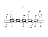
まず、半導体装置を交換する場合の問題点を説明する。図1は、BGA型の半導体装置2を実装した回路基板4の部分断面図である。図1には、半導体装置2及びその近傍が図示されている。
(Embodiment 1)
First, problems in replacing a semiconductor device will be described. FIG. 1 is a partial sectional view of a
回路基板4は、半導体装置2と配線基板6を有している。ここで、半導体装置2は、半導体素子8(集積回路が形成された半導体チップ)と、表面に半導体素子8を搭載したインターポーザ10と、半導体素子8を覆うカバー12を有している。インターポーザ10の裏面には、半導体装置2の外部電極14が2次元アレイ状に設けられている。
The
この外部電極14に対応して、配線基板6の表面には、基板電極(ランド)16が2次元アレイ状に設けられている。そして、半導体装置2の外部電極14と基板電極16が、半田18によって接続されている。この半田18は、半導体装置2の外部電極14に設けられていた半田ボールが溶融して、基板電極16に密着したものである。
Corresponding to the
図2は、半導体装置2を配線基板6から取り外した状態を説明する断面図である。半導体装置2を取り外すには、まず半導体装置2を半田18の融点以上に加熱して、半田18を溶融させる。その後、半導体装置2を引き上げて、半導体装置2を配線基板6から取り外す。この時、半田18の一部が、基板電極16に取り残される。この時取り残される半田18aの量は、図2に示すように、基板電極16ごとに異なっており均一ではない。このため、新しい半導体装置の実装前に、取り残された半田18aを除去することが好ましい。しかし、配線基板6には他の電子部品も実装されており、残留半田18aの除去は容易ではない。すなわち、半導体装置の交換には、残留半田18aの除去が容易できないという問題がある。
FIG. 2 is a cross-sectional view illustrating a state where the
(1)回路基板の構造
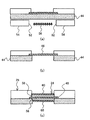
図3は、上記問題を解決した本実施の形態の回路基板20の部分断面図である。図3には、半導体装置2及びその近傍が図示されている。
(1) Structure of Circuit Board FIG. 3 is a partial cross-sectional view of the
本実施の形態の回路基板20は、図3に示すように、外部電極14が底面に設けられた半導体装置2と、外部電極14に対応する基板電極16を有する配線基板6と、中継基板22とを有している。
As shown in FIG. 3, the
図4は、中継基板22の断面図である。中継基板22は、図4に示すように、半導体装置2の外部電極14に対応する複数の第1の貫通電極24を有する第1の絶縁基板26と、外部電極14に対応する複数の第2の貫通電極28を有する第2の絶縁基板30とを有している。ここで、第1の貫通電極24と第2の貫通電極28は、第1の半田32を介して接続されている。
FIG. 4 is a cross-sectional view of the
そして、図3に示すように、本実施の形態の回路基板20では、半導体装置2の外部電極14と中継基板22の第1の貫通電極24が、第2の半田34を介して接続されている。また、配線基板6の基板電極16と中継基板22の第2の貫通電極28が、第3の半田36を介して接続されている。ここで、第1の半田32(図4参照)は、第2の半田34及び第3の半田36より低い融点を有している。更に、第1の半田32は、第2の半田34より薄い厚さを有している。
As shown in FIG. 3, in the
第2の半田34は、例えば、半導体装置2の外部電極14に設けられた半田ボールが溶融して、第1の貫通電極24(図4参照)に密着した半田である。従って、第2の半田は、例えば半田ボールに広く用いられている重量比が1:1:0.5のSn-Ag-Cu(以下、SAC合金と呼ぶ)合金であり、その融点は220℃である。同様に、第3の半田も、SAC合金である。一方、第1の半田は、例えば重量比が42:58のSn-Bi(以下、Sn-58Biと呼ぶ)合金であり、その融点は139℃である。
The
ところで、中継基板を用いずに配線基板に半導体装置を直接実装する場合、まず配線基板に半導体装置を載置し、その後配線基板を加熱して半導体装置の半田ボールを溶融させる。次に、配線基板を冷却して溶融した半田ボールを凝固させて、半導体装置の外部電極と配線基板の基板電極(ランド)を接続する。この冷却過程で、熱膨張率の違いにより、半導体装置と配線基板の双方に歪(以下、熱歪と呼ぶ)が発生する。 When a semiconductor device is directly mounted on a wiring board without using a relay board, the semiconductor device is first placed on the wiring board, and then the wiring board is heated to melt the solder balls of the semiconductor device. Next, the solder balls melted by cooling the wiring substrate are solidified to connect the external electrodes of the semiconductor device and the substrate electrodes (lands) of the wiring substrate. During this cooling process, strain (hereinafter referred to as thermal strain) occurs in both the semiconductor device and the wiring board due to the difference in thermal expansion coefficient.
半導体装置(特に、一辺が40〜70mmの大型のBGA型半導体装置)には、通常、直径400〜900μmの比較的大きな半田ボールが設けられている。このような大きな半田ボールを用いることにより、半導体装置と配線基板の熱膨張率の違いにより発生する熱歪を緩和することができる。 A semiconductor device (in particular, a large BGA type semiconductor device having a side of 40 to 70 mm) is usually provided with a relatively large solder ball having a diameter of 400 to 900 μm. By using such a large solder ball, it is possible to relieve the thermal strain caused by the difference in coefficient of thermal expansion between the semiconductor device and the wiring board.
従って、本回路基板20においても、第2の半田34の厚さは、500μm以上900μm以下が好ましく、600μm以上800以下μmが更に好ましい。
Therefore, also in this
尚、第2の半田34の代わりに、第3の半田36を第1の半田32より厚くしてもよい。或いは、第2の半田34及び第3の半田36の双方を、第1の半田32より厚くしてもよい。これらの場合、第3の半田36の好ましい厚さは、第2の半田34と同じである。
Note that the
(2)半導体装置の交換方法
次に、上記回路基板20における半導体装置2の交換方法について説明する。図5及び6は、半導体装置2の交換方法を説明する工程断面図である。
(2) Method for Replacing Semiconductor Device Next, a method for replacing the
まず、第1の半田32の融点(例えば、139℃)より高く且つ第2の半田34及び第3の半田36の融点(例えば、220℃)より低い温度(例えば、145℃)に半導体装置2をヒーターで加熱して、第1の半田32だけを溶融する。その後半導体装置2を引き上げて、図5(a)に示すように、半導体装置2と第1の絶縁基板26とを有する部材38を配線基板6から取り外す。
First, the
上述したように、第1の半田32の厚さは、半田バンプからなる第2の半田34より薄い。従って、第2の貫通電極28には、多くの半田は取り残されない。このため、半田を除去しなくても、半導体装置2を再実装することができる。ここで、第1の半田32の厚さは250μm以下が好ましく、200μm以下が更に好ましい。但し、薄過ぎると貫通電極同士の接続が困難になるので、第1の半田32の厚さは50μm以上が好ましく、100μm以上が更に好ましい。
As described above, the thickness of the
次に、配線基板6を冷却して、取り残された第1の半田32aを凝固させる。その後、図5(b)に示すように、上記部材38に対応する交換対象の部材40(以下、交換部材と呼ぶ)を、第2の絶縁基板30に載置する。ここで、交換部材40は、新たな半導体装置2aと、半導体装置2aの外部電極14aに対応する第3の貫通電極24aを有する第3の絶縁基板26aとを有し、外部電極14aと第3の貫通電極24aが第4の半田(例えば、SAC半田)34aを介して接続されている。更に、図5(b)に示すように、第3の貫通電極24aの(半導体装置2aの)反対側の面には、第5の半田32b(例えば、Sn-58Bi半田)が設けられている。
Next, the
ここで、第5の半導体32bの融点(例えば、139℃)は、第2乃至4の半田34,36, 34aの融点(例えば、220℃)より低い。また、第5の半田32bの厚さは、第2の半田34又は第3の半田36より薄い(例えば、50μm以上250μm以下、または100μm以上200μm以下)。
Here, the melting point (for example, 139 ° C.) of the
次に、取り残された第1の半田32a及び第5の半田32bの融点(例えば、139℃)より高く、且つ第3の半田36及び第4の半田34aの融点(例えば、220℃)より低い温度(例えば、150℃)に半導体装置2aをヒーターで加熱し、その後冷却する。これにより、取り残された第1の半田32aと第5の半田32bが一体化して、図6に示すように、交換部材40の第3の貫通電極24aと、第2の絶縁基板30の第2の貫通電極28が接続する。
Next, the melting point (for example, 139 ° C.) of the left
以上のように、本実施の形態によれば、取り残された第1の半田32aを除去せずに、半導体装置2を交換することができる。このため、半導体装置2の交換が容易になる。
As described above, according to the present embodiment, the
ところで、第1の絶縁基板26だけで中継基板を形成して、低融点半田(例えば、Sn-58Bi半田)でその貫通電極を基板電極(ランド)16に接続するようにしても、半導体装置2の交換は容易になるようにも思われる。但し、この場合には、他の電子部品も、低融点半田で基板電極に接続することになる。このため、交換する半導体装置38を加熱した時に、他の電子部品の低融点半田も同時に溶解してしまう。従って、第1の絶縁基板26だけ中継基板を形成することは好ましくない。
By the way, the
また、中継基板を第2の絶縁基板30だけで形成して、低融点半田(例えば、Sn-58Bi半田)でその貫通電極と半導体装置の外部電極を接続することも考えられる。しかし、外部電極に低融点半田ボールを設けた半導体装置2は流通しておらず、入手困難である。従って、このような方法も採用することはできない。
It is also conceivable that the relay substrate is formed only by the second insulating
(3)中継基板の製造方法
次に、製造方法にしたがって、中継基板22の構造を詳しく説明する。
(3) Method for Manufacturing Relay Board Next, according to the manufacturing method, the structure of the
図7乃至11は、中継基板22の製造方法を説明する工程断面図である。尚、図7乃至10は、第1の貫通電極24の近傍を拡大した断面図である。
7 to 11 are process cross-sectional views illustrating a method for manufacturing the
―貫通電極の形成工程(図7〜図9参照)―
まず、図7(a)に示すように、厚さ0.035mmのCu箔42を片面に貼り付けた厚さ0.05mmのポリイミドフィルム44を準備する。このポリイミドフィルム44は、一辺が40mmの正方形である。
—Penetration electrode formation process (see FIGS. 7 to 9) —
First, as shown to Fig.7 (a), the 0.05-mm-
次に、図7(b)に示すように、Cu箔42の表面に、半導体装置2の外部電極14に対応する直径0.8mmのフォトレジストパターン46を形成する。この時、フォトレジストパターン46を、1mmピッチで40行×40列に2次元配列する。
Next, as shown in FIG. 7B, a
次に、図7(c)に示すように、フォトレジストパターン46をエッチングマスクとしてCu箔42をエッチングして、第1の貫通電極24のベース層48を形成する。
Next, as shown in FIG. 7C, the
次に、図8(a)に示すように、フォトレジストパターン46を除去する。その後、図8(b)に示すように、ベース層48の外周部を覆う、直径0.6mmの開口部51が設けられたカバー層50を形成する。カバー層50は、例えばポリイミド膜又はソルダレジストである。
Next, as shown in FIG. 8A, the
次に、ベース層48に対応する開口部52を有するメタルマスク54を、ポリイミドフィルム44の裏面に配置する。この時、ベース層48と開口部52を対向させる。開口部52の直径は、0.6mmである。
Next, a
次に、図9(a)に示すように、メタルマスク54で覆われたポリイミドフィルム44にレーザ光56を照射する。このレーザ光照射により、図9(b)に示すように開口部52のポリイミドフィルム44が除去され、ベース層48が露出する。
Next, as shown in FIG. 9A, the
次に、図9(c)に示すように、無電解メッキによりベース層48の両面に、Niバリア層58及びAu半田付層60を順次積層する。
Next, as shown in FIG. 9C, the
以上により、第1の貫通電極24を有する第1の絶縁基板26が完成する。同様の手順により、第2の貫通電極28を有する第2の絶縁基板30を形成する。
Thus, the first insulating
ところで、第1の絶縁基板26及び第2の絶縁基板30は、ポリイミドフィルムから形成されているので、可撓性を有している。このため、回路基板20の熱歪に対して、中継基板22は柔軟に対応することができる。
By the way, since the 1st insulating
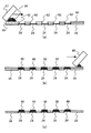
次に、図10(a)及び(b)に示すように、第1の貫通電極24に対応する開口部62を有するメタルマスク64とスキジ67を用いて、第1の貫通電極24の片面に半田ペースト66を印刷する。この半田ペースト66の主成分は、Sn-52Bi粒子(融点139℃)である。メタルマスク64の厚さは、0.2mmである。これにより、第1の貫通電極24の片面に、厚さ約0.1mmの半田ペースト66が塗布される(図10(c)参照)。
Next, as shown in FIGS. 10A and 10B, a
次に、この第1の絶縁基板26に最高温度160℃のリフロー処理を施して、半田ペースト66を溶融する。その後、第1の絶縁基板26を冷却して、図11(a)に示すように、第1の貫通電極24の片面を覆う半田層68を形成する。同様の処理を第2の絶縁基板30にも施して、第2の貫通電極28の片面を覆う半田層を形成する。
Next, the first insulating
次に、図11(b)に示すように、第1の絶縁基板26と第2の絶縁基板30を、夫々の半田層が接触するように重ね合わせる。その後、第1の絶縁基板26と第2の絶縁基板30をリフロー炉で加熱して、第1の絶縁基板26と第2の絶縁基板30夫々の半田層を溶融して一体化させ、厚さ150μmの第1の半田32を形成する。以上により、中継基板22が完成する。
Next, as shown in FIG. 11B, the first insulating
以上の例では、Cu箔をエッチングしたベース層48の両面にNiバリア層58及びAu半田付層60を積層して、第1の貫通電極24及び第2の貫通電極28を形成する。しかし、単にCu箔42をエッチングして、第1の貫通電極24及び第2の貫通電極28を形成してもよい。この場合、Cu箔42への半田層68の拡散を防止するため、Cu箔42を少なくても10μm程度厚くすることが好ましい。
In the above example, the
尚、ポリイミドフィルム44等に貫通孔(ビア)を形成し、この貫通孔をCu、Al、又はAl合金等の導電性材料で埋め込んで貫通電極を形成してもよい。更に、貫通孔を埋め込んだ導電性材料の両面にNi層とAu層を順次積層して、貫通電極を形成してもよい。
In addition, a through-hole (via) may be formed in the
(4)回路基板の製造方法
次に、製造方法にしたがって、本実施の形態の回路基板20の構造を詳しく説明する。
(4) Circuit Board Manufacturing Method Next, the structure of the
図12は、本実施の形態の回路基板20の製造方法を説明する工程断面図である。
FIG. 12 is a process cross-sectional view illustrating the method for manufacturing the
まず、図12(a)に示すように、中継基板22と、半導体装置2と、この半導体装置2の外部電極14に対応する基板電極16を有する配線基板6とを準備する。
First, as shown in FIG. 12A, a
配線基板6は、厚さ約4mmで110×110mm角のガラスエポキシ製のプリント基板である。基板電極16は、配線基板6の中央に40行×40列に2次元配列されている。基板電極16はCu製であり、直径は0.6mmである。この基板電極16には、SAC半田層70が印刷されている。
The
半導体装置2のインターポーザ10は、厚さが1.5mmのガラスセラミック板である。このインターポーザ10には、Au/Ni製の外部電極14が2次元アレイ状に設けられている。外部電極14の直径は0.6mmである。この外部電極14には、直径の0.6mmのSAC半田ボール72が設けられている。
The
次に、基板電極16と、中継基板22の貫通電極24,28と、半導体装置2の外部電極14が鉛直線上に整列するように、配線基板6と中継基板22と半導体装置2とを順次重ね合わせる(図12(a)参照)。
Next, the
次に、図12(b)に示すように、重ね合わせた各部材2,22,6に、最高温度235℃のリフロー処理を施して、各部材に設けた半田を溶融する。
Next, as shown in FIG. 12B, the
次に、図12(c)に示すように、リフロー処理を施した各部材2,22,6を冷却して、中継基板22の第1の貫通電極24と半導体装置2の外部電極14を第2の半田34(半田ボール72)を介して接続する。同時に、中継基板22の第2の貫通電極28と配線基板6の基板電極16を、第3の半田36(SAC半田層70)を介して接続する。以上により、回路基板20が完成する。
Next, as shown in FIG. 12C, the reflow-treated
ところで、リフロー処理後の冷却過程では、最初に第2の半田34(SAC半田)及び第3の半田36(SAC半田)が凝固し、その後第1の半田32(Sn-58Bi半田)が凝固する。従って、配線基板6と半導体装置2は、第1の半田32の融点(139℃)までは、夫々自由に熱収縮する。しかし、第1の半田32の凝固後は、配線基板6と半導体装置2は、第1乃至3の半田32,34,36を介して互いに固定され、自由に収縮できなくなる。このため、図12(c)に示すように、配線基板6及び半導体装置2に反り74が発生する。しかし、第1の半田32の融点(139℃)が第2の半田34及び第3の半田36の融点(220℃)より低いので、反り74は、半導体装置2と配線基板6をSAC半田バンプ(融点220℃)で直接接続する回路基板4の反り76より小さくなる(図1参照)。
Incidentally, in the cooling process after the reflow process, first, the second solder 34 (SAC solder) and the third solder 36 (SAC solder) are solidified, and then the first solder 32 (Sn-58Bi solder) is solidified. . Accordingly, the
例えば、半導体装置2の一辺が40mmの場合、本実施の形態の回路基板20の反りは、0.01mm〜0.05mmである。しかし、半導体装置2と配線基板6をSAC半田バンプで直接接続した回路基板の反りは、0.1mm〜0.3mmである。
For example, when one side of the
以上のように、本実施の形態の回路基板20によれば、半導体装置の交換が容易になるだけでなく、回路基板の反りを抑制することができる。
As described above, according to the
(実施の形態2)
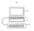
図13は、本実施の形態のパーソナルコンピュータ78の構成図である。
(Embodiment 2)
FIG. 13 is a configuration diagram of the
図13に示すように、本パーソナルコンピュータ78は、実施の形態1の回路基板20(マザーボード)と、回路基板20に入力信号を供給する入力信号供給ユニット(キーボード80及びハードディスク82)と、回路基板の出力信号を受信して処理する出力信号処理ユニット84(液晶表示装置)とを有している。
As shown in FIG. 13, the
上述したように、回路基板20における半導体装置2の交換は容易なので、パーソナルコンピュータ78の製造歩留りは高い。尚、本実施の形態は、他の電子機器、例えばサーバや携帯電話にも適用できる。
As described above, since the replacement of the
以上の例では、第1の半田32は、Sn−58Bi合金である。しかし、第1の半田32は、重量比52:48のIn-Sn合金(融点117℃)等の他の半田であってもよい。また、夫々の合金の重量比は、上述した値に限られない。従って、第1の半田32には、種々の重量比のSn-Bi合金及びIn-Sn合金や他の合金を用いてもよい。
In the above example, the
以上の実施の形態に関し、更に以下の付記を開示する。 Regarding the above embodiment, the following additional notes are disclosed.
2・・・半導体装置
6・・・配線基板
14・・・外部電極
16・・・基板電極
20・・・回路基板
22・・・中継基板
24・・・第1の貫通電極
26・・・第1の絶縁基板
28・・・第2の貫通電極
30・・・第2の絶縁基板
32・・・第1の半田
34・・・第2の半田
36・・・第3の半田
38・・・部材
40・・・交換部材
78・・・パーソナルコンピュータ(電子機器)
2 ...
Claims (7)
前記外部電極に対応する基板電極を有する配線基板と、
前記外部電極に対応する第1の貫通電極を有する第1の絶縁基板と、前記外部電極に対応する第2の貫通電極を有する第2の絶縁基板とを有し、前記第1の貫通電極と前記第2の貫通電極が第1の半田を介して接続された中継基板とを備え、
前記外部電極と前記第1の貫通電極が、第2の半田を介して接続され、
前記基板電極と前記第2の貫通電極が、第3の半田を介して接続され、
前記第1の半田が、前記第2の半田及び前記第3の半田より低い融点を有し、且つ前記第2の半田又は前記第3の半田より薄い回路基板。 A semiconductor device provided with an external electrode on one side;
A wiring substrate having a substrate electrode corresponding to the external electrode;
A first insulating substrate having a first through electrode corresponding to the external electrode; and a second insulating substrate having a second through electrode corresponding to the external electrode; and The second through electrode includes a relay substrate connected via a first solder;
The external electrode and the first through electrode are connected via a second solder,
The substrate electrode and the second through electrode are connected via a third solder,
A circuit board in which the first solder has a lower melting point than the second solder and the third solder and is thinner than the second solder or the third solder.
前記第1の絶縁基板及び前記第2の絶縁基板は、可撓性を有することを、
特徴とする回路基板。 The circuit board according to claim 1,
The first insulating substrate and the second insulating substrate have flexibility.
Feature circuit board.
前記第1の半田は、SnBi半田又はInSn半田であり、
前記第2の半田及び前記第3の半田は、SnAgCu半田であることを、
特徴とする回路基板。 The circuit board according to claim 1 or 2,
The first solder is SnBi solder or InSn solder,
The second solder and the third solder are SnAgCu solder,
Feature circuit board.
前記外部電極に対応する第1の貫通電極を有する第1の絶縁基板と、
前記外部電極に対応し、第1の半田を介して前記第1の貫通電極に接続された第2の貫通電極を有する第2の絶縁基板とを備え、
前記第1の半田より融点が高い第2の半田を介して、記第1の貫通電極が前記外部電極に接続され、前記第1の半田より融点が高い第3の半田を介して、前記第2の貫通電極が前記基板電極に接続され、前記第1の半田が、前記第2の半田又は第3の半田より薄い中継基板。 A relay substrate provided between a semiconductor device having an external electrode provided on one surface and a wiring board having a substrate electrode corresponding to the external electrode,
A first insulating substrate having a first through electrode corresponding to the external electrode;
A second insulating substrate corresponding to the external electrode and having a second through electrode connected to the first through electrode via a first solder;
The first through electrode is connected to the external electrode via a second solder having a melting point higher than that of the first solder, and the third solder is connected to the external electrode via a third solder having a melting point higher than that of the first solder. A relay substrate in which two through electrodes are connected to the substrate electrode, and the first solder is thinner than the second solder or the third solder.
前記回路基板に入力信号を供給する入力信号供給ユニットと、
前記回路基板の出力信号を受信して処理する出力信号処理ユニットとを、
有する電子機器。 Corresponding to a semiconductor device in which an external electrode is provided on one surface, a wiring board having a substrate electrode corresponding to the external electrode, a first insulating substrate having a first through electrode corresponding to the external electrode, and the external electrode A second insulating substrate having a second through electrode, and the first through electrode and a relay substrate to which the second through electrode is connected via a first solder, and the external electrode And the first through electrode are connected via a second solder, the substrate electrode and the second through electrode are connected via a third solder, and the first solder is the second solder. And a circuit board having a lower melting point than the third solder and thinner than the second solder or the third solder;
An input signal supply unit for supplying an input signal to the circuit board;
An output signal processing unit for receiving and processing the output signal of the circuit board;
Electronic equipment that has.
前記中継基板を準備した後に、
前記第1の貫通電極と前記外部電極を前記第2の半田を介して接続し、前記第2の貫通電極と前記基板電極を前記第3の半田を介して接続する回路基板の製造方法。 Corresponding to a semiconductor device in which an external electrode is provided on one surface, a wiring board having a substrate electrode corresponding to the external electrode, a first insulating substrate having a first through electrode corresponding to the external electrode, and the external electrode A second insulating substrate having a second through electrode, and the first through electrode and a relay substrate to which the second through electrode is connected via a first solder, and the external electrode And the first through electrode are connected via a second solder, the substrate electrode and the second through electrode are connected via a third solder, and the first solder is the second solder. And a method of manufacturing a circuit board having a melting point lower than that of the third solder and thinner than the second solder or the third solder,
After preparing the relay board,
A method of manufacturing a circuit board, wherein the first through electrode and the external electrode are connected through the second solder, and the second through electrode and the substrate electrode are connected through the third solder.
前記第1の半田の融点より高く且つ前記第2の半田及び前記第3の半田の融点より低い温度に前記半導体装置を加熱して、前記半導体装置と前記第1の絶縁基板とを有する部材を前記配線基板から取り外す第1の工程と、
前記第1の工程の後、前記部材の交換対象の部材の貫通電極と前記第2の貫通電極を接続する第2工程とを有する
半導体装置の交換方法。 Corresponding to a semiconductor device in which an external electrode is provided on one surface, a wiring board having a substrate electrode corresponding to the external electrode, a first insulating substrate having a first through electrode corresponding to the external electrode, and the external electrode A second insulating substrate having a second through electrode, and the first through electrode and a relay substrate to which the second through electrode is connected via a first solder, and the external electrode And the first through electrode are connected via a second solder, the substrate electrode and the second through electrode are connected via a third solder, and the first solder is the second solder. And a method of replacing a semiconductor device of a circuit board having a lower melting point than the third solder and thinner than the second solder or the third solder,
A member having the semiconductor device and the first insulating substrate by heating the semiconductor device to a temperature higher than the melting point of the first solder and lower than the melting points of the second solder and the third solder. A first step of removing from the wiring board;
A method for replacing a semiconductor device, comprising, after the first step, a second step of connecting the through electrode of the member to be replaced with the second through electrode.
Priority Applications (1)
| Application Number | Priority Date | Filing Date | Title |
|---|---|---|---|
| JP2010064617A JP5407967B2 (en) | 2010-03-19 | 2010-03-19 | Circuit board, electronic device, circuit board manufacturing method, and semiconductor device replacement method |
Applications Claiming Priority (1)
| Application Number | Priority Date | Filing Date | Title |
|---|---|---|---|
| JP2010064617A JP5407967B2 (en) | 2010-03-19 | 2010-03-19 | Circuit board, electronic device, circuit board manufacturing method, and semiconductor device replacement method |
Publications (2)
| Publication Number | Publication Date |
|---|---|
| JP2011199029A JP2011199029A (en) | 2011-10-06 |
| JP5407967B2 true JP5407967B2 (en) | 2014-02-05 |
Family
ID=44876871
Family Applications (1)
| Application Number | Title | Priority Date | Filing Date |
|---|---|---|---|
| JP2010064617A Expired - Fee Related JP5407967B2 (en) | 2010-03-19 | 2010-03-19 | Circuit board, electronic device, circuit board manufacturing method, and semiconductor device replacement method |
Country Status (1)
| Country | Link |
|---|---|
| JP (1) | JP5407967B2 (en) |
Families Citing this family (2)
| Publication number | Priority date | Publication date | Assignee | Title |
|---|---|---|---|---|
| JP6019555B2 (en) * | 2011-09-07 | 2016-11-02 | 富士通株式会社 | Semiconductor device, method for reproducing semiconductor device, and method for manufacturing semiconductor device |
| JP6512231B2 (en) * | 2017-01-27 | 2019-05-15 | トヨタ自動車株式会社 | Semiconductor device |
Family Cites Families (7)
| Publication number | Priority date | Publication date | Assignee | Title |
|---|---|---|---|---|
| JPH09307225A (en) * | 1996-05-13 | 1997-11-28 | Hitachi Ltd | Printed board |
| JP2001119113A (en) * | 1999-10-20 | 2001-04-27 | Sony Corp | Semiconductor device and method of manufacturing semiconductor device |
| JP2002100711A (en) * | 2000-09-25 | 2002-04-05 | Oki Electric Ind Co Ltd | Semiconductor device package mounting structure, mounting method and repair method |
| JP3813497B2 (en) * | 2001-11-12 | 2006-08-23 | 株式会社ルネサステクノロジ | Bump forming method and semiconductor device mounting structure |
| JP4949718B2 (en) * | 2006-04-06 | 2012-06-13 | アルプス電気株式会社 | Electronic component mounting structure |
| JP2009105095A (en) * | 2007-10-19 | 2009-05-14 | Advantest Corp | Devices and equipment |
| JP2010045246A (en) * | 2008-08-14 | 2010-02-25 | Fujitsu Ltd | Board unit and method for manufacturing the same |
-
2010
- 2010-03-19 JP JP2010064617A patent/JP5407967B2/en not_active Expired - Fee Related
Also Published As
| Publication number | Publication date |
|---|---|
| JP2011199029A (en) | 2011-10-06 |
Similar Documents
| Publication | Publication Date | Title |
|---|---|---|
| KR100996914B1 (en) | Chip embedded printed circuit board and its manufacturing method | |
| US7670939B2 (en) | Semiconductor chip bump connection apparatus and method | |
| CN108476585B (en) | PCB Hybrid Redistribution Layer | |
| US20100044845A1 (en) | Circuit substrate, an electronic device arrangement and a manufacturing process for the circuit substrate | |
| CN102843877B (en) | A printed wiring board and a method for manufacturing the printed wiring board | |
| JP2010098278A (en) | Printed circuit board having round solder bump and method of manufacturing the same | |
| JP2015207580A (en) | Wiring board and manufacturing method of the same | |
| JP2015226046A (en) | Semiconductor device, manufacturing method of the same, and electronic apparatus | |
| JP2020004926A (en) | Wiring board and method of manufacturing wiring board | |
| JP5407967B2 (en) | Circuit board, electronic device, circuit board manufacturing method, and semiconductor device replacement method | |
| JP6601055B2 (en) | Printed wiring board, electronic device and mounting method | |
| JP2014045190A (en) | Method for manufacturing printed-circuit board | |
| JP2018186121A (en) | Semiconductor package substrate, semiconductor package, and semiconductor device | |
| JP4172238B2 (en) | Electronic component mounting structure | |
| JP2001077518A (en) | Electronic component mounting printed circuit board and electronic component removal method | |
| JP4561193B2 (en) | Printed wiring board and semiconductor device | |
| JP2024134789A (en) | Semiconductor device and wiring board | |
| JP7087369B2 (en) | Manufacturing method of carrier substrate with fine wiring layer and semiconductor package substrate with fine wiring layer | |
| JP2011249457A (en) | Wiring board having embedded component, and manufacturing method for the same | |
| JP4599891B2 (en) | Semiconductor device substrate and semiconductor device | |
| JP5062022B2 (en) | Electronic component equipment | |
| JP5359993B2 (en) | Component built-in wiring board, method of manufacturing component built-in wiring board | |
| TWI420989B (en) | Printed circuit board and method of manufacturing the same | |
| JP2013102020A (en) | Semiconductor package substrate | |
| JP5115241B2 (en) | Electronic component mounting method |
Legal Events
| Date | Code | Title | Description |
|---|---|---|---|
| A621 | Written request for application examination |
Free format text: JAPANESE INTERMEDIATE CODE: A621 Effective date: 20130108 |
|
| TRDD | Decision of grant or rejection written | ||
| A01 | Written decision to grant a patent or to grant a registration (utility model) |
Free format text: JAPANESE INTERMEDIATE CODE: A01 Effective date: 20131008 |
|
| A977 | Report on retrieval |
Free format text: JAPANESE INTERMEDIATE CODE: A971007 Effective date: 20131010 |
|
| A61 | First payment of annual fees (during grant procedure) |
Free format text: JAPANESE INTERMEDIATE CODE: A61 Effective date: 20131021 |
|
| R150 | Certificate of patent or registration of utility model |
Ref document number: 5407967 Country of ref document: JP Free format text: JAPANESE INTERMEDIATE CODE: R150 |
|
| LAPS | Cancellation because of no payment of annual fees |