JP5407523B2 - Integrating AD converter, solid-state imaging device, and camera system - Google Patents
Integrating AD converter, solid-state imaging device, and camera system Download PDFInfo
- Publication number
- JP5407523B2 JP5407523B2 JP2009107105A JP2009107105A JP5407523B2 JP 5407523 B2 JP5407523 B2 JP 5407523B2 JP 2009107105 A JP2009107105 A JP 2009107105A JP 2009107105 A JP2009107105 A JP 2009107105A JP 5407523 B2 JP5407523 B2 JP 5407523B2
- Authority
- JP
- Japan
- Prior art keywords
- signal
- comparator
- main clock
- latch
- timing
- Prior art date
- Legal status (The legal status is an assumption and is not a legal conclusion. Google has not performed a legal analysis and makes no representation as to the accuracy of the status listed.)
- Active
Links
Images


Classifications
-
- H—ELECTRICITY
- H03—ELECTRONIC CIRCUITRY
- H03M—CODING; DECODING; CODE CONVERSION IN GENERAL
- H03M1/00—Analogue/digital conversion; Digital/analogue conversion
- H03M1/12—Analogue/digital converters
- H03M1/14—Conversion in steps with each step involving the same or a different conversion means and delivering more than one bit
-
- H—ELECTRICITY
- H04—ELECTRIC COMMUNICATION TECHNIQUE
- H04N—PICTORIAL COMMUNICATION, e.g. TELEVISION
- H04N25/00—Circuitry of solid-state image sensors [SSIS]; Control thereof
- H04N25/70—SSIS architectures; Circuits associated therewith
- H04N25/76—Addressed sensors, e.g. MOS or CMOS sensors
- H04N25/767—Horizontal readout lines, multiplexers or registers
-
- H—ELECTRICITY
- H04—ELECTRIC COMMUNICATION TECHNIQUE
- H04N—PICTORIAL COMMUNICATION, e.g. TELEVISION
- H04N25/00—Circuitry of solid-state image sensors [SSIS]; Control thereof
- H04N25/70—SSIS architectures; Circuits associated therewith
- H04N25/76—Addressed sensors, e.g. MOS or CMOS sensors
- H04N25/78—Readout circuits for addressed sensors, e.g. output amplifiers or A/D converters
-
- H—ELECTRICITY
- H03—ELECTRONIC CIRCUITRY
- H03M—CODING; DECODING; CODE CONVERSION IN GENERAL
- H03M1/00—Analogue/digital conversion; Digital/analogue conversion
- H03M1/12—Analogue/digital converters
- H03M1/1205—Multiplexed conversion systems
- H03M1/123—Simultaneous, i.e. using one converter per channel but with common control or reference circuits for multiple converters
-
- H—ELECTRICITY
- H03—ELECTRONIC CIRCUITRY
- H03M—CODING; DECODING; CODE CONVERSION IN GENERAL
- H03M1/00—Analogue/digital conversion; Digital/analogue conversion
- H03M1/12—Analogue/digital converters
- H03M1/50—Analogue/digital converters with intermediate conversion to time interval
- H03M1/56—Input signal compared with linear ramp
-
- H—ELECTRICITY
- H03—ELECTRONIC CIRCUITRY
- H03M—CODING; DECODING; CODE CONVERSION IN GENERAL
- H03M1/00—Analogue/digital conversion; Digital/analogue conversion
- H03M1/12—Analogue/digital converters
- H03M1/64—Analogue/digital converters with intermediate conversion to phase of sinusoidal or similar periodical signals
Landscapes
- Engineering & Computer Science (AREA)
- Multimedia (AREA)
- Signal Processing (AREA)
- Theoretical Computer Science (AREA)
- Transforming Light Signals Into Electric Signals (AREA)
- Analogue/Digital Conversion (AREA)
Description
本発明は、CMOSイメージセンサに代表される固体撮像素子に適用可能な積分型AD変換装置、固体撮像素子、およびカメラシステムに関するものである。 The present invention relates to an integral AD converter, a solid-state image sensor, and a camera system that can be applied to a solid-state image sensor represented by a CMOS image sensor.
たとえば高解像度の撮像を高速で行う固体撮像素子に搭載可能な積分型アナログ−デジタル変換装置(以下、AD変換装置(Analog Digital Converter)という)が提案されている(特許文献1参照)。 For example, an integration type analog-to-digital converter (hereinafter referred to as an AD converter (Analog Digital Converter)) that can be mounted on a solid-state imaging device that performs high-resolution imaging at high speed has been proposed (see Patent Document 1).
特許文献1には、クロック周波数を上げずに分解能を向上させる積分型AD変換装置が提案されている。
この積分型AD変換装置は、通常の上位ビットカウンタとリング発振器によって位相の異なるクロック信号をラッチとデコードをする時間量子化器(TDC: Time-to-Digital Converter)で下位ビットの情報を得、クロック周波数を上げずに分解能を向上させる。
This integrating AD converter obtains lower bit information by a time quantizer (TDC: Time-to-Digital Converter) that latches and decodes clock signals having different phases by a normal upper bit counter and a ring oscillator, Improve resolution without increasing clock frequency.
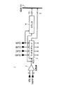
図1は、特許文献1に開示されたAD変換装置の構成を示す図である。
FIG. 1 is a diagram illustrating a configuration of an AD conversion apparatus disclosed in
このAD変換装置1は、比較器2、TDC(時間量子化器、ラッチおよびデコード)3、上位ビットカウンタ4、および転送バス5を有する。
この例は、位相が45°ずつ異なるクロック信号4本を用いて、上位カウンタで11ビット(bit)、下位TDCで3ビットの計14ビットの分解能を持つ積分型AD変換器である。
時間とともに電圧値が線形に変化するランプ波形の参照電圧RAMPと入力電圧VSLとを比較器2で比較し、比較結果は信号VCOとして出力される。
信号VCOが変化したタイミングで上位カウンタ4は動作を開始もしくは停止し、また下位TDCでは位相の異なるクロック信号の情報をラッチする。
The
This example is an integrating AD converter using four clock signals whose phases are different by 45 ° and having a resolution of 14 bits in total, that is, 11 bits in the upper counter and 3 bits in the lower TDC.
The
At the timing when the signal VCO changes, the
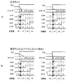
図2は、クロック周波数よりこまかな分解能を得る下位TDCの原理を示す図である。 FIG. 2 is a diagram showing the principle of the low-order TDC that obtains finer resolution than the clock frequency.
クロック周波数の1周期の中において、信号VCOが変化するタイミングで、位相が45°ずつ異なる4つのクロック信号CLKA、CLKB、CLKC、CLKDの値をラッチすると8通りの拡張コードEB[3:0]が得られる。
この8通りのコードをTDC3のラッチおよびデコード部でデコードして3ビットの下位ビットの情報を得ることができる。
この例では、信号VCOが変化するタイミングで上位ビットカウンタ4がカウントを開始する後カウント方式の例である。
When the values of four clock signals CLKA, CLKB, CLKC, and CLKD that are different in phase by 45 ° are latched at the timing when the signal VCO changes in one cycle of the clock frequency, eight extension codes EB [3: 0] Is obtained.
The eight types of codes can be decoded by the latch and decoding unit of the
This example is an example of a post-counting method in which the
図3は、信号VCOが変化するタイミングが各クロックのエッジの前後で変化した場合に得られる拡張コードEB[3:0]のバイナリ値とデコードした結果の変化を示す図である。 FIG. 3 is a diagram illustrating a change in the binary value of the extension code EB [3: 0] obtained when the timing at which the signal VCO changes before and after the edge of each clock and the result of decoding.
通常ではデコード値の変化は±1LSBであり連続しているが、クロックCLKAの立ち上りエッジの前後では上位リップルカウンタとの接続によっては±7LSBの誤差を発生してしまう。これをスパークルエラーと呼ぶ。 Normally, the change in the decode value is ± 1 LSB and is continuous. However, before and after the rising edge of the clock CLKA, an error of ± 7 LSB is generated depending on the connection with the upper ripple counter. This is called a sparkle error.
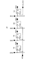
図4(A)および(B)は、上位ビットカウンタと下位TDCのつなぎ部分において、連続に正しくカウントされる場合と、スパークルエラーが生じてしまう場合を示す図である。 FIGS. 4A and 4B are diagrams showing a case where the upper bit counter and the lower TDC are continuously counted correctly and a case where a sparkle error occurs.
クロック信号CLKAは上位ビットカウンタ4のクロック信号と下位TDCの位相差クロック信号と共通している。
信号VCOがクロック信号CLKAの立ち上りエッジ前後で変化した場合にスパークルエラーは発生する可能性がある。
信号VCOがクロック信号CLKAの立ち上りエッジのわずかに前に変化した場合、拡張コードEB[3:0]は[0000b]が記憶され、直後のクロック信号CLKAの立ち上りエッジで上位ビットカウンタ4がカウントした場合正しいカウントとなる。
また、信号VCOがクロック信号CLKAの立ち上りエッジのわずかに後に変化した場合、拡張コードEB[3:0]は[1000b]が記憶される。
そして、直前のクロック信号CLKAの立ち上りエッジでは上位ビットカウンタ4がカウントせず次の立ち上りエッジまで待つのも正しいカウントとなる。
The clock signal CLKA is common to the clock signal of the
A sparkle error may occur when the signal VCO changes before and after the rising edge of the clock signal CLKA.
When the signal VCO changes slightly before the rising edge of the clock signal CLKA, [0000b] is stored as the extension code EB [3: 0], and the
When the signal VCO changes slightly after the rising edge of the clock signal CLKA, [1000b] is stored as the extension code EB [3: 0].
Then, the
しかしながら、下位TDCにおいて拡張コードがラッチされるタイミングと上位ビットカウンタにおいてカウントの開始のタイミングが異なった場合、この関係が逆転する現象が生ずる。
すなわち、信号VCOがクロック信号CLKAの立ち上りエッジのわずかに前に変化した場合において、拡張コードEB[3:0]は[0000b]が記憶されている。
直後のクロック信号CLKAの立ち上りエッジで上位カウンタがカウントをしない場合や、信号VCOがクロック信号CLKAの立ち上りエッジのわずかに後に変化した場合において、拡張コードEB[3:0]は[1000b]が記憶されている。
しかし、直前のクロック信号CLKAの立ち上りエッジで上位ビットカウンタ4がカウントしてしまう場合が生じうる。このときにスパークルエラーが生じてしまう。
However, when the timing at which the extension code is latched in the lower TDC and the count start timing in the upper bit counter are different, a phenomenon in which this relationship is reversed occurs.
That is, when the signal VCO changes slightly before the rising edge of the clock signal CLKA, [0000b] is stored as the extension code EB [3: 0].
When the upper counter does not count at the rising edge of the clock signal CLKA immediately after that, or when the signal VCO changes slightly after the rising edge of the clock signal CLKA, [1000b] is stored as the extension code EB [3: 0]. Has been.
However, the
特許文献1に記載された方式では信号VCOにあたる信号が上位ビットカウンタ4と下位TDC3に別々に入力されており、その内部において回路遅延が存在する。
このため、厳密に上位ビットカウンタ4がカウントを停止するタイミングと下位TDC3の位相情報をラッチするタイミングが同一であることを保証できないため、スパークルエラーが発生する可能性がある。
In the method described in
For this reason, it is not possible to guarantee that the timing at which the
本発明は、スパークルエラーの発生を防止することが可能な積分型AD変換装置、固体撮像素子、およびカメラシステムを提供することにある。 An object of the present invention is to provide an integral AD converter, a solid-state imaging device, and a camera system that can prevent the occurrence of a sparkle error.
本発明の第1の観点の積分型AD変換装置は、時間とともに電圧値が線形に変化するランプ波形の参照電圧と入力電圧とを比較する比較器と、前記比較器の出力信号が反転したことをトリガとして動作開始または動作停止し、主クロック信号の周期ごとに計数する上位ビットカウンタと、位相の異なる前記主クロックを含む複数のクロック信号を用いて前記比較器の出力信号が反転したタイミングで位相情報をラッチし、当該ラッチした値をデコードすることでクロック周期より分解能が高い下位ビットを出力する時間量子化器と、前記比較器の出力信号と前記主クロック信号の同期化を行い、同期化を行った結果の信号を用いて、上位ビットカウンタの動作開始および停止のタイミングと、前記主クロック信号の位相情報をラッチする値を決定する調整部とを有する。 In the integrating AD converter according to the first aspect of the present invention, a comparator for comparing a reference voltage of a ramp waveform whose voltage value linearly changes with time and an input voltage, and an output signal of the comparator are inverted. At the timing when the output signal of the comparator is inverted using a high-order bit counter that starts or stops the operation with a trigger as a trigger and counts for each period of the main clock signal and a plurality of clock signals including the main clock with different phases. Latch the phase information and decode the latched value to synchronize the time quantizer that outputs lower bits with higher resolution than the clock period, the output signal of the comparator and the main clock signal Using the resulting signal, the timing for starting and stopping the operation of the upper bit counter and the value for latching the phase information of the main clock signal are obtained. And a regulating portion fixed to.
本発明の第2の観点の固体撮像素子は、光電変換を行う複数の画素が行列状に配列された画素部と、前記画素部から複数の画素単位で画素信号の読み出しを行う画素信号読み出し部と、を有し、前記画素信号読み出し部は、画素の列配列に対応して、読み出したアナログ信号をデジタル信号に変換する積分型アナログデジタル(AD)変換装置を有し、前記積分型AD変換装置は、ランプ波である参照電圧が供給され、供給された参照電圧と当該列の画素の読み出しアナログ信号電位とを比較する複数の比較器と、時間とともに電圧値が線形に変化するランプ波形の参照電圧と該列の画素の読み出しアナログ信号電位とを比較する比較器と、前記比較器の出力信号が反転したことをトリガとして動作開始または動作停止し、主クロック信号の周期ごとに計数する上位ビットカウンタと、位相の異なる前記主クロックを含む複数のクロック信号を用いて前記比較器の出力信号が反転したタイミングで位相情報をラッチし、当該ラッチした値をデコードすることでクロック周期より分解能が高い下位ビットを出力する時間量子化器と、前記比較器の出力信号と前記主クロック信号の同期化を行い、同期化を行った結果の信号を用いて、上位ビットカウンタの動作開始および停止のタイミングと、前記主クロック信号の位相情報をラッチする値を決定する調整部と、を含む。 A solid-state imaging device according to a second aspect of the present invention includes a pixel unit in which a plurality of pixels that perform photoelectric conversion are arranged in a matrix, and a pixel signal readout unit that reads out pixel signals from the pixel unit in units of a plurality of pixels. The pixel signal readout unit includes an integration type analog-to-digital (AD) conversion device that converts the read analog signal into a digital signal corresponding to the column arrangement of the pixels, and the integration type AD conversion. The apparatus is supplied with a reference voltage that is a ramp wave, a plurality of comparators that compare the supplied reference voltage with the readout analog signal potential of the pixel in the column, and a ramp waveform whose voltage value changes linearly with time. A comparator that compares the reference voltage with the readout analog signal potential of the pixel in the column, and the operation start or stop is triggered by the inversion of the output signal of the comparator, and the main clock signal The phase information is latched at the timing when the output signal of the comparator is inverted using a plurality of clock signals including the main clock having different phases and the upper bit counter that counts every period, and the latched value is decoded. in using the time quantizer resolution than the clock cycle to output a high lower bits, the have line synchronization of the comparator output signal and said main clock signal, a signal of a result of the synchronization, the upper bits A timing for starting and stopping the counter, and an adjustment unit for determining a value for latching phase information of the main clock signal.
本発明の第3の観点のAD変換装置は、固体撮像素子と、前記固体撮像素子に被写体像を結像する光学系と、を有し、前記固体撮像素子は、光電変換を行う複数の画素が行列状に配列された画素部と、前記画素部から複数の画素単位で画素信号の読み出しを行う画素信号読み出し部と、を有し、前記画素信号読み出し部は、画素の列配列に対応して、読み出したアナログ信号をデジタル信号に変換する積分型アナログデジタル(AD)変換装置を有し、前記積分型AD変換装置は、ランプ波である参照電圧が供給され、供給された参照電圧と当該列の画素の読み出しアナログ信号電位とを比較する複数の比較器と、時間とともに電圧値が線形に変化するランプ波形の参照電圧と該列の画素の読み出しアナログ信号電位とを比較する比較器と、前記比較器の出力信号が反転したことをトリガとして動作開始または動作停止し、主クロック信号の周期ごとに計数する上位ビットカウンタと、位相の異なる前記主クロックを含む複数のクロック信号を用いて前記比較器の出力信号が反転したタイミングで位相情報をラッチし、当該ラッチした値をデコードすることでクロック周期より分解能が高い下位ビットを出力する時間量子化器と、前記比較器の出力信号と前記主クロック信号の同期化を行い、同期化を行った結果の信号を用いて、上位ビットカウンタの動作開始および停止のタイミングと、前記主クロック信号の位相情報をラッチする値を決定する調整部と、を含む。 An AD conversion apparatus according to a third aspect of the present invention includes a solid-state imaging device and an optical system that forms a subject image on the solid-state imaging device, and the solid-state imaging device includes a plurality of pixels that perform photoelectric conversion. Are arranged in a matrix, and a pixel signal readout unit that reads out pixel signals from the pixel unit in units of a plurality of pixels, and the pixel signal readout unit corresponds to a column arrangement of pixels. The integrated analog-to-digital (AD) converter that converts the read analog signal into a digital signal, the integrated AD converter is supplied with a reference voltage that is a ramp wave, and the supplied reference voltage A plurality of comparators for comparing read analog signal potentials of pixels in a column, a comparator for comparing a reference voltage of a ramp waveform whose voltage value linearly changes with time, and read analog signal potentials of the pixels of the column; The operation is started or stopped by using the inverted output signal of the comparator as a trigger, and the upper bit counter that counts every period of the main clock signal, and a plurality of clock signals including the main clocks having different phases are used. The phase information is latched at the timing when the output signal of the comparator is inverted, and the time quantizer that outputs lower bits having a resolution higher than the clock period by decoding the latched value; the output signal of the comparator; and There line synchronization of the main clock signal by using a signal of a result of the synchronization, the operation start and stop timings of the upper bit counter, adjusting unit for determining the value of latching the phase information of the main clock signal And including.
本発明によれば、スパークルエラーの発生を防止することができる。 According to the present invention, the occurrence of a sparkle error can be prevented.
以下、本発明の実施の形態を図面に関連付けて説明する。
なお、説明は以下の順序で行う。
1.第1の実施形態(AD変換装置の構成例)
2.第2の実施形態(固体撮像素子の全体構成例)
3.第3の実施形態(カメラシステムの構成例)
Hereinafter, embodiments of the present invention will be described with reference to the drawings.
The description will be given in the following order.
1. First Embodiment (Configuration Example of AD Converter)
2. Second Embodiment (Overall Configuration Example of Solid-State Image Sensor)
3. Third Embodiment (Configuration Example of Camera System)
<1.第1の実施形態>
[AD変換装置の構成例]
図5は、本発明の第1の実施形態に係る積分型AD変換装置に構成例を示す図である。
<1. First Embodiment>
[Configuration example of AD converter]
FIG. 5 is a diagram illustrating a configuration example of the integral AD converter according to the first embodiment of the present invention.
本第1の実施形態に係るAD変換装置10は、比較器11、上位ビットカウンタ12、調整部13、TDC(Time-to-Digital Converter:時間量子化器)14、および転送バス15を有する。
The
比較器11は、時間とともに電圧値が線形に変化するランプ波形の参照電圧RAMPと入力電圧VSLとを比較し、その結果に応じたレベルの信号VCOを調整部13およびTDC14に出力する。
The
上位ビットカウンタ12は、基本的に、比較器11の出力信号VCOが反転したことをトリガとして動作開始もしくは動作停止し、主クロック信号CLKAの周期ごとに計数する機能を有する。
上位ビットカウンタ12は、調整部13により比較器11の出力信号VCOと主クロックCLKAと同期させて生成されたカウント動作開始信号VCO_SYNCをトリガとして、調整部13を介した主クロック信号CLKAOの周期ごとに計数する。
The upper bit counter 12 basically has a function of starting or stopping the operation triggered by the inversion of the output signal VCO of the
The upper bit counter 12 is triggered by the count operation start signal VCO_SYNC generated by the
調整部13は、比較器11の出力信号VCOと主クロック信号CLKAの同期化を行い、同期化を行った結果の信号を用いて、上位ビットカウンタ12の動作開始および停止のタイミングと、主クロック信号CLKAの位相情報をラッチする値を決定する。
調整部13は、比較器11の出力信号VCOを主クロック信号CLKAの立ち上がりと立ち下がりの両エッジで同期化し、この同期化信号をカウント動作開始信号VCO_SYNCとして出力する同期化回路131を有する。
調整部13は、カウント動作開始信号VCO_SYNCを基に主クロック信号CLKAの位相情報をラッチするラッチタイミング信号VCO_SYNCDを生成し、ラッチタイミング信号VCO_SYNCDをTDC14に出力する機能を有する。
調整部13は、カウント動作開始信号VCO_SYNCを遅延させてラッチタイミング信号VCO_SYNCDを生成し、ラッチタイミング信号VCO_SYNCDをTDC14に出力する遅延部132を含む。
The
The
The
The
図6は、本実施形態に係る調整部の同期化回路の構成例を示す回路図である。
図6は、同期化回路131のゲートレベルの回路図である。
FIG. 6 is a circuit diagram illustrating a configuration example of the synchronization circuit of the adjustment unit according to the present embodiment.
FIG. 6 is a circuit diagram of the gate level of the
同期化回路131は、クロック信号CLKAの立ち上りと立下りの両エッジで信号VCOを同期化する必要があるため、2つのFF131,FF132、およびNANDゲートNA131を有している。
また、同期化回路131は、主クロック信号CLKAを遅延させてクロック信号CLKAOを生成し、上位ビットカウンタ12に出力する、直列接続されたインバータINV131,INV132を有する。
本例では、インバータINV131の出力であるクロック信号CK1およびインバータINV132の出力であるクロック信号CK2がFF131,FF132にクロック信号として供給される。
なお、主クロックCLKAとインバータINV131の出力であるクロック信号CK1を、FF131,FF132のクロック信号として供給することも可能である。
The
The
In this example, the clock signal CK1 that is the output of the inverter INV131 and the clock signal CK2 that is the output of the inverter INV132 are supplied to the FF131 and FF132 as clock signals.
Note that the main clock CLKA and the clock signal CK1 that is the output of the inverter INV131 can be supplied as the clock signals of the FF131 and FF132.
FF131は、入力段の転送ゲートTM11、ラッチLTC11、クロックドインバータCIV11、ラッチLTC12、およびノードND11〜ND14を有する。
ラッチLTC11は、インバータINV11およびクロックドインバータCIV12により形成されている。
ラッチLTC12は、インバータINV12およびクロックドインバータCIV13により形成されている。
The
Latch LTC11 is formed by an inverter INV11 and a clocked
Latch LTC12 is formed by an inverter INV12 and a clocked
転送ゲートTM11は、PMOSトランジスタとNMOSトランジスタのソースドレイン同士を接続して構成される。PMOSトランジスタのゲートにクロック信号CK1が供給され、NMOSトランジスタのゲートにクロック信号CK2が供給される。
転送ゲートTM11の一方の入出力端子が比較器11の出力信号VCOの供給ラインに接続され、他方の入出力端子がノードND11に接続されている。
The transfer gate TM11 is configured by connecting the source and drain of a PMOS transistor and an NMOS transistor. The clock signal CK1 is supplied to the gate of the PMOS transistor, and the clock signal CK2 is supplied to the gate of the NMOS transistor.
One input / output terminal of the transfer gate TM11 is connected to the supply line of the output signal VCO of the
ラッチLTC11は、インバータINV11の入力端子がノードND11に接続され、出力端子がノードND12に接続されている。クロックドインバータCIV12の入力端子がノードND12に接続され、出力端子がノードND11に接続されている。
クロックドインバータCIV12は、正側クロック端子にクロック信号CK1が供給され、負側クロック端子にクロック信号CK2が供給される。
In the latch LTC11, the input terminal of the inverter INV11 is connected to the node ND11, and the output terminal is connected to the node ND12. An input terminal of the clocked inverter CIV12 is connected to the node ND12, and an output terminal is connected to the node ND11.
In the clocked inverter CIV12, the clock signal CK1 is supplied to the positive clock terminal, and the clock signal CK2 is supplied to the negative clock terminal.
クロックドインバータCIV11の入力端子がノードND12に接続され、出力端子がノードND13に接続されている。
クロックドインバータCIV11は、正側クロック端子にクロック信号CK1が供給され、負側クロック端子にクロック信号CK2が供給される。
An input terminal of the clocked inverter CIV11 is connected to the node ND12, and an output terminal is connected to the node ND13.
In the clocked inverter CIV11, the clock signal CK1 is supplied to the positive clock terminal, and the clock signal CK2 is supplied to the negative clock terminal.
ラッチLTC12は、インバータINV12の入力端子がノードND13に接続され、出力端子がノードND14に接続されている。クロックドインバータCIV13の入力端子がノードND14に接続され、出力端子がノードND13に接続されている。
クロックドインバータCIV13は、負側クロック端子にクロック信号CK1が供給され、正側クロック端子にクロック信号CK2が供給される。
そして、ラッチLTC12の出力ノードとしてのノードND14がNANDゲートNA131の一方の入力端子に接続されている。
In the latch LTC12, the input terminal of the inverter INV12 is connected to the node ND13, and the output terminal is connected to the node ND14. An input terminal of the clocked inverter CIV13 is connected to the node ND14, and an output terminal is connected to the node ND13.
In the clocked inverter CIV13, the clock signal CK1 is supplied to the negative clock terminal, and the clock signal CK2 is supplied to the positive clock terminal.
A node ND14 as an output node of the latch LTC12 is connected to one input terminal of the NAND gate NA131.
このような構成を有するFF131は、クロック信号CK1の立ち下がりで、クロック信号CK2の立ち上がりのタイミングで比較器11の出力信号VCOをラッチLTC11側に取り込む。
次に、クロック信号CK1の立ち上がりで、クロック信号CK2の立ち下がりのタイミングでクロックドインバータCIV12が作動し、信号VCOがラッチLTC11にラッチされる。そして、そのラッチ信号がクロックドインバータCIV11を介してラッチLTC12側に転送される。
次に、クロック信号CK1の立ち下がりで、クロック信号CK2の立ち上がりのタイミングでクロックドインバータCIV13が作動し、転送された信号VCOがラッチLTC12にラッチされる。
また、ノードND14のラッチ信号がNANDゲートNA131の一方の入力端子に供給される。
The
Next, the clocked inverter CIV12 operates at the rising edge of the clock signal CK1 and the falling edge of the clock signal CK2, and the signal VCO is latched in the latch LTC11. Then, the latch signal is transferred to the latch LTC12 side via the clocked inverter CIV11.
Next, at the falling edge of the clock signal CK1, the clocked inverter CIV13 operates at the rising timing of the clock signal CK2, and the transferred signal VCO is latched in the latch LTC12.
The latch signal at the node ND14 is supplied to one input terminal of the NAND gate NA131.
このように、FF131では、クロック信号の立ち下がりエッジに同期して比較器11の出力信号VCOを取り込み、ラッチする。
Thus, the
FF132は、入力段の転送ゲートTM21、ラッチLTC21、クロックドインバータCIV21、ラッチLTC22、およびノードND21〜ND24を有する。
ラッチLTC21は、インバータINV21およびクロックドインバータCIV22により形成されている。
ラッチLTC22は、インバータINV22およびクロックドインバータCIV23により形成されている。
The
Latch LTC21 is formed by an inverter INV21 and a clocked inverter C IV 22.
Latch LTC22 is formed by an inverter INV22 and a clocked
転送ゲートTM21は、PMOSトランジスタとNMOSトランジスタのソースドレイン同士を接続して構成される。NMOSトランジスタのゲートにクロック信号CK1が供給され、PMOSトランジスタのゲートにクロック信号CK2が供給される。
転送ゲートTM21の一方の入出力端子が比較器11の出力信号VCOの供給ラインに接続され、他方の入出力端子がノードND21に接続されている。
The transfer gate TM21 is configured by connecting the source and drain of a PMOS transistor and an NMOS transistor. The clock signal CK1 is supplied to the gate of the NMOS transistor, and the clock signal CK2 is supplied to the gate of the PMOS transistor.
One input / output terminal of the transfer gate TM21 is connected to the supply line of the output signal VCO of the
ラッチLTC21は、インバータINV21の入力端子がノードND21に接続され、出力端子がノードND22に接続されている。クロックドインバータCIV22の入力端子がノードND22に接続され、出力端子がノードND21に接続されている。
クロックドインバータCIV22は、負側クロック端子にクロック信号CK1が供給され、正側クロック端子にクロック信号CK2が供給される。
In the latch LTC21, the input terminal of the inverter INV21 is connected to the node ND21, and the output terminal is connected to the node ND22. An input terminal of clocked inverter CIV22 is connected to node ND22, and an output terminal is connected to node ND21.
In the clocked inverter CIV22, the clock signal CK1 is supplied to the negative clock terminal, and the clock signal CK2 is supplied to the positive clock terminal.
クロックドインバータCIV21の入力端子がノードND22に接続され、出力端子がノードND23に接続されている。
クロックドインバータCIV21は、負側クロック端子にクロック信号CK1が供給され、正側クロック端子にクロック信号CK2が供給される。
The input terminal of clocked inverter CIV21 is connected to node ND22, and the output terminal is connected to node ND23.
In the clocked inverter CIV21, the clock signal CK1 is supplied to the negative clock terminal, and the clock signal CK2 is supplied to the positive clock terminal.
ラッチLTC22は、インバータINV22の入力端子がノードND23に接続され、出力端子がノードND24に接続されている。クロックドインバータCIV23の入力端子がノードND24に接続され、出力端子がノードND23に接続されている。
クロックドインバータCIV23は、正側クロック端子にクロック信号CK1が供給され、負側クロック端子にクロック信号CK2が供給される。
そして、ラッチLTC22の出力ノードとしてのノードND24がNANDゲートNA131の他方の入力端子に接続されている。
The latch LTC22 has an input terminal of the inverter INV22 connected to the node ND23 and an output terminal connected to the node ND24. An input terminal of the clocked inverter CIV23 is connected to the node ND24, and an output terminal is connected to the node ND23.
In the clocked inverter CIV23, the clock signal CK1 is supplied to the positive clock terminal, and the clock signal CK2 is supplied to the negative clock terminal.
A node ND24 as an output node of the latch LTC22 is connected to the other input terminal of the NAND gate NA131.
このような構成を有するFF132は、クロック信号CK1の立ち上がりで、クロック信号CK2の立ち下がりのタイミングで比較器11の出力信号VCOをラッチLTC21側に取り込む。
次に、クロック信号CK1の立ち下がりで、クロック信号CK2の立ち上がりのタイミングでクロックドインバータCIV22が作動し、信号VCOがラッチLTC21にラッチされる。そして、そのラッチ信号がクロックドインバータCIV21を介してラッチLTC22側に転送される。
次に、クロック信号CK1の立ち上がりで、クロック信号CK2の立ち下がりのタイミングでクロックドインバータCIV23が作動し、転送された信号VCOがラッチLTC22にラッチされる。
また、ノードND24のラッチ信号がNANDゲートNA131の他方の入力端子に供給される。
The
Next, at the falling edge of the clock signal CK1, the clocked inverter CIV22 operates at the rising timing of the clock signal CK2, and the signal VCO is latched in the latch LTC21. Then, the latch signal is transferred to the latch LTC22 side via the clocked inverter CIV21.
Next, at the rising edge of the clock signal CK1, the clocked inverter CIV23 operates at the falling edge of the clock signal CK2, and the transferred signal VCO is latched in the latch LTC22.
The latch signal at the node ND24 is supplied to the other input terminal of the NAND gate NA131.
FF132では、クロック信号の立ち上がりエッジに同期して比較器11の出力信号VCOを取り込み、ラッチする。
The
以上のように、同期化回路131においては、比較器11の出力信号VCOが2つのFF131、FF132に入力され、FF131、FF132は互いに主クロック信号CLKAの反対のエッジで取り込まれるように構成されている。
比較器11の出力信号VCOと主クロック信号CLKAは同期化回路131に入力され、信号VCOは主クロック信号CLKAの立ち上りおよび立下りエッジで同期化される。
同期化された信号はVCO_SYNCとして出力され、この信号をトリガとして上位ビットカウンタ12のカウント動作開始信号となる。
また、信号VCO_SYNCは遅延素子を間に挟み、ラッチタイミング信号VCO_SYNCDとして下位TDC14における主クロック信号CLKAのラッチに入力される。
As described above, in the
The output signal VCO of the
The synchronized signal is output as VCO_SYNC, and becomes a count operation start signal of the upper bit counter 12 using this signal as a trigger.
The signal VCO_SYNC is input to the latch of the main clock signal CLKA in the
TDC14は、基本的に、位相の異なる主クロックCLKAを含む複数のクロック信号を用いて比較器11の出力信号VCOが反転したタイミングで位相情報をラッチし、ラッチした値をデコードすることでクロック周期より分解能が高い下位ビットを出力する。
本例では、位相の異なる複数のクロック信号として、主クロック信号CLKAを基準に位相が45°ずつ順にずれたクロック信号CLKA,CLKB,CLBC,CLKDが用いられる。
The
In this example, clock signals CLKA, CLKB, CLBC, CLKD whose phases are sequentially shifted by 45 ° with respect to the main clock signal CLKA are used as a plurality of clock signals having different phases.
図7は、本実施形態に係るTDC(時間量子化器)のラッチ部の構成例を示す図である。 FIG. 7 is a diagram illustrating a configuration example of a latch unit of the TDC (time quantizer) according to the present embodiment.
図5のTDC14のラッチ部140は、第1のラッチとしてのフリップフロップ(FF)141,142,143、および第2のラッチとしてのFF144を有する。
第1のラッチとしてのFF141〜143はそれぞれ、比較器11の出力信号VCOに同期して主クロック信号CLKAを除く、クロック信号CLKB,CLKC,CLKDの位相情報をラッチする。
The
The
FF141は、比較器11の出力信号VCOに同期してクロック信号CLKDの位相情報をラッチする。FF141のQ出力からは拡張コードEB[0]が得られる。
FF142は、比較器11の出力信号VCOに同期してクロック信号CLKCの位相情報をラッチする。FF142のQ出力からは拡張コードEB[1]が得られる。
FF143は、比較器11の出力信号VCOに同期してクロック信号CLKBの位相情報をラッチする。FF143のQ出力からは拡張コードEB[2]が得られる。
The
The
The
FF144は、調整部13により生成されるラッチタイミング信号VCO_SYNCDに同期して主クロック信号CLKAの位相情報をラッチする。FF144のQ出力からは拡張コードEB[3]が得られる。
第2ラッチとしてのFF144は、主クロック信号CLKAの論理とは反転した値を出力する。
The
The
図8は、本実施形態に係るTDC(時間量子化器)の第1のラッチとしてのFFの具体的な構成例を示す回路図である。
図8は、第1のラッチとしてのFF141〜143のゲートレベルの回路図である。
ここでは、FF143の構成が例示されているが、FF141、FF142もFF143と同様の構成を有する。
FIG. 8 is a circuit diagram showing a specific configuration example of the FF as the first latch of the TDC (time quantizer) according to the present embodiment.
FIG. 8 is a circuit diagram of the gate level of the
Here, the configuration of the
FF143は、インバータINV31,INV32、クロックドインバータCIV31、CIV32、ラッチLTC31,LTC32、NORゲートNR31、およびノードND31〜ND34を有している。
ラッチLTC31は、インバータINV33およびクロックドインバータCIV33により形成されている。
ラッチLTC32は、NORゲートNR31およびクロックドインバータCIV34により形成されている。
The
The latch LTC31 is formed by an inverter INV33 and a clocked inverter CIV33.
The latch LTC32 is formed by a NOR gate NR31 and a clocked inverter CIV34.
インバータINV31の入力端子は比較器11の出力信号VCOの供給ラインに接続されている。
クロックドインバータCIV31の入力端子がクロック信号CLKBの供給ラインに接続され、出力端子がノードND31に接続されている。
クロックドインバータCIV31は、正側クロック端子に比較器11の出力信号VCOの反転信号が供給され、負側クロック端子に信号VCOが供給される。
The input terminal of the inverter INV31 is connected to the supply line of the output signal VCO of the
The input terminal of the clocked inverter CIV31 is connected to the supply line of the clock signal CLKB, and the output terminal is connected to the node ND31.
In the clocked inverter CIV31, the inverted signal of the output signal VCO of the
ラッチLTC31は、インバータINV33の入力端子がノードND31に接続され、出力端子がノードND32に接続されている。クロックドインバータCIV33の入力端子がノードND32に接続され、出力端子がノードND31に接続されている。
クロックドインバータCIV33は、負側クロック端子に比較器11の出力信号VCOの反転信号が供給され、正側クロック端子に信号VCOが供給される。
Latch LT C 31 is the input terminal of the inverter INV33 is connected to the node ND31, an output terminal connected to the node ND32. An input terminal of the clocked inverter CIV33 is connected to the node ND32, and an output terminal is connected to the node ND31.
In the clocked inverter CIV33, the inverted signal of the output signal VCO of the
クロックドインバータCIV32は、入力端子がノードND32に接続され、出力端子がノードND33に接続されている。
クロックドインバータCIV32は、負側クロック端子に比較器11の出力信号VCOの反転信号が供給され、正側クロック端子に信号VCOが供給される。
Clocked inverter CIV32 has an input terminal connected to the node ND32, and an output terminal connected to the
In the clocked inverter CIV32, an inverted signal of the output signal VCO of the
ラッチLTC32は、NORゲートNR31の一方の入力端子がノードND33に接続され、出力端子がノードND34に接続されている。クロックドインバータCIV34の入力端子がノードND34に接続され、出力端子がノードND33に接続されている。
クロックドインバータCIV34は、正側クロック端子に比較器11の出力信号VCOの反転信号が供給され、負側クロック端子に信号VCOが供給される。
また、NORゲートNR31の他方の入力端子はインバータINV32の出力端子に接続され、インバータINV32の入力端子はリセット系信号XRSTの供給ラインに接続されている。
Latch LT C 32, one input terminal of the NOR gate NR31 is connected to the node ND33, an output terminal connected to the node ND34. An input terminal of the clocked inverter CIV34 is connected to the node ND34, and an output terminal is connected to the node ND33.
In the clocked inverter CIV34, the inverted signal of the output signal VCO of the
The other input terminal of the NOR gate NR31 is connected to the output terminal of the inverter INV32, the input terminal of the inverter INV32 is connected to the supply line of the reset system signal XRST.
このような構成を有するFF143は、比較器11の出力信号VCOの立ち下がりのタイミングでクロック信号CLKBをラッチLTC31側に取り込む。
次に、信号VCOの立ち上がりのタイミングでクロックドインバータCIV33が作動し、クロックCLKBがラッチLTC31にラッチされる。そして、そのラッチ信号がクロックドインバータCIV32を介してラッチLTC32側に転送される。
次に、信号VCOの立ち下がりタイミングでクロックドインバータCIV34が作動し、転送されたクロック信号CLKBがラッチLTC32にラッチされる。
そして、ノードND34のラッチ信号が拡張コードEB[2]として出力される。
The
Next, the clocked inverter CIV 33 operates at the rising timing of the signal VCO, and the clock CLKB is latched in the latch LTC31. Then, the latch signal is transferred to the latch LTC 32 side via the clocked inverter CIV 32 .
Next, the clocked inverter CIV34 operates at the falling timing of the signal VCO, and the transferred clock signal CLKB is latched in the latch LTC32.
Then, the latch signal of the node ND34 is output as the extension code EB [2].
このように、図8のFF143(141,142)は、クロック信号CLKB,CLKC,CLKDの位相情報をラッチして拡張コードEB[2:0]を出力するFFである。
FF143(141,142)は、ラッチタイミング信号は比較器11の出力信号VCOであり、クロック信号CLKB,CLKC,CLKDの値がそのまま取り込まれ出力される。
As described above, the FF 143 (141, 142) in FIG. 8 is an FF that latches the phase information of the clock signals CLKB, CLKC, and CLKD and outputs the extended code EB [2: 0].
In the FF 143 (141, 142), the latch timing signal is the output signal VCO of the
図9は、本実施形態に係る調整部の遅延部およびTDC(時間量子化器)の第1のラッチとしてのFFの具体的な構成例を示す回路図である。
図9は、遅延部および第2のラッチとしてのFF144のゲートレベルの回路図である。
FIG. 9 is a circuit diagram illustrating a specific configuration example of the FF as the delay unit of the adjustment unit and the first latch of the TDC (time quantizer) according to the present embodiment.
FIG. 9 is a circuit diagram of the gate level of the
調整部13の遅延部132は、たとえば図9に示すように、遅延素子であるインバータINV132−1〜INV132−n(図9の例ではn=4)を直列に接続したインバータチェーンにより形成される。
遅延部132は、同期化回路131から出力されるカウント動作開始信号VCO_SYNCを所定時間遅延させてラッチタイミング信号VCO_SYNCDとしてTDC14のFF144に供給する。
For example, as shown in FIG. 9, the
The
FF144は、インバータINV41、クロックドインバータCIV41、CIV42、ラッチLTC41,LTC42、NANDゲートNA41、およびノードND41〜ND44を有している。
ラッチLTC41は、インバータINV42およびクロックドインバータCIV43により形成されている。
ラッチLTC42は、NANDゲートNA41およびクロックドインバータCIV44により形成されている。
The
The latch LTC41 is formed by an inverter INV42 and a clocked inverter CIV43.
The latch LTC42 is formed by a NAND gate NA41 and a clocked inverter CIV44.
インバータINV41の入力端子はラッチタイミング信号VCO_SYNCDの供給ラインに接続されている。
クロックドインバータCIV41の入力端子が主クロック信号CLKAの供給ラインに接続され、出力端子がノードND41に接続されている。
クロックドインバータCIV41は、正側クロック端子にラッチタイミング信号VCO_SYNCDの反転信号が供給され、負側クロック端子にラッチタイミング信号VCO_SYNCDが供給される。
The input terminal of the inverter INV41 is connected to the supply line of the latch timing signal VCO_SYNCD.
An input terminal of the clocked inverter CIV41 is connected to the supply line of the main clock signal CLKA, and an output terminal is connected to the node ND41.
In the clocked inverter CIV41, an inverted signal of the latch timing signal VCO_SYNCD is supplied to the positive clock terminal, and the latch timing signal VCO_SYNCD is supplied to the negative clock terminal.
ラッチLTC41は、インバータINV42の入力端子がノードND41に接続され、出力端子がノードND42に接続されている。クロックドインバータCIV43の入力端子がノードND42に接続され、出力端子がノードND41に接続されている。
クロックドインバータCIV43は、負側クロック端子にラッチタイミング信号VCO_SYNCDの反転信号が供給され、正側クロック端子にラッチタイミング信号VCO_SYNCDが供給される。
Latch LT C 41 is an input terminal of the inverter INV42 is connected to the node ND41, an output terminal connected to the node ND42. The input terminal of the clocked inverter CIV43 is connected to the node ND42, and the output terminal is connected to the node ND41.
In the clocked inverter CIV43, the inverted signal of the latch timing signal VCO_SYNCD is supplied to the negative clock terminal, and the latch timing signal VCO_SYNCD is supplied to the positive clock terminal.
クロックドインバータCIV42は、入力端子がノードND42に接続され、出力端子がノードND43に接続されている。
クロックドインバータCIV42は、負側クロック端子にラッチタイミング信号VCO_SYNCDの反転信号が供給され、正側クロック端子にラッチタイミング信号VCO_SYNCDが供給される。
Clocked inverter CIV42 has an input terminal connected to the node ND42, an output terminal connected to a
In the clocked inverter CIV42, the inverted signal of the latch timing signal VCO_SYNCD is supplied to the negative clock terminal, and the latch timing signal VCO_SYNCD is supplied to the positive clock terminal.
ラッチLTC42は、NANDゲートNA41の一方の入力端子がノードND43に接続され、出力端子がノードND44に接続されている。クロックドインバータCIV44の入力端子がノードND44に接続され、出力端子がノードND43に接続されている。
クロックドインバータCIV44は、正側クロック端子にラッチタイミング信号VCO_SYNCDの反転信号が供給され、負側クロック端子にラッチタイミング信号VCO_SYNCDが供給される。
また、NANDゲートNA41の他方の入力端子はリセット系信号XRSTの供給ラインに接続されている。
Latch LT C 42, one input terminal of the NAND gate NA41 is connected to the node ND43, an output terminal connected to the node ND44. An input terminal of the clocked inverter CIV44 is connected to the node ND44, and an output terminal is connected to the node ND43.
In the clocked inverter CIV44, the inverted signal of the latch timing signal VCO_SYNCD is supplied to the positive clock terminal, and the latch timing signal VCO_SYNCD is supplied to the negative clock terminal.
The other input terminal of the NAND gate NA41 is connected to the supply line of the reset signal XRST.
このような構成を有するFF144は、ラッチタイミング信号VCO_SYNCDの立ち下がりのタイミングで主クロック信号CLKAをラッチLTC41側に取り込む。
次に、ラッチタイミング信号VCO_SYNCDの立ち上がりのタイミングでクロックドインバータCIV43が作動し、主クロックCLKAがラッチLTC41にラッチされる。そして、そのラッチ信号がクロックドインバータCIV42を介してラッチLTC42側に転送される。
次に、ラッチタイミング信号VCO_SYNCDの立ち下がりタイミングでクロックドインバータCIV44が作動し、転送された主クロック信号CLKAがラッチLTC42にラッチされる。
そして、ノードND43のラッチ信号が拡張コードEB[3]として出力される。
The
Next, the clocked inverter CIV43 operates at the rising timing of the latch timing signal VCO_SYNCD, and the main clock CLKA is latched in the latch LTC41. Then, the latch signal is transferred to the latch LTC42 side via the clocked
Next, the clocked inverter CIV44 operates at the falling timing of the latch timing signal VCO_SYNCD, and the transferred main clock signal CLKA is latched in the latch LTC42.
Then, the latch signal of the node ND43 is output as the extension code EB [3].
このように、FF144は、主クロック信号CLKAの位相情報をラッチして拡張コードをEB[3]を出力するFFである。
ラッチタイミング信号VCO_SYNCDはカウント動作開始信号VCO_SYNCをインバータチェーンのような遅延部132によって遅延させて生成される。
拡張コードEB[3]は記憶されるべき値と実際に取り込む値が逆となるため、拡張コードEB[3]の出力は主クロック信号CLKAの論理とは反転した値が出力されるようになっている。
As described above, the
The latch timing signal VCO_SYNCD is generated by delaying the count operation start signal VCO_SYNC by a
Since the value to be stored in the extension code EB [3] is opposite to the value that is actually captured, the output of the extension code EB [3] is a value that is inverted from the logic of the main clock signal CLKA. ing.
以上の構成を有する積分型AD変換装置10は、上位ビットカウンタ12と下位ビットTDC14とのつなぎで生ずるスパークルエラーの発生を防止することを特徴とする。
The
ここで、本実施形態の積分型AD変換装置10がスパークルエラーを防止する原理について、図10および図11に関連付けて説明する。
図10および図11は、本実施形態に係る積分型AD変換装置におけるスパークルエラー防止の原理を説明するため図である。
Here, the principle that the
10 and 11 are diagrams for explaining the principle of sparkle error prevention in the integral AD converter according to the present embodiment.
図11は、比較器の出力信号VCOが主クロック信号CLKAの立ち上りエッジのわずかに前に変化した場合を示している。 Figure 1 1 shows a case where the output signal VCO of the comparator changes slightly before the rising edge of the main clock signal CLKA.
拡張コード[2:0]は主クロック信号CLKAのエッジ前後にかかわらず[000b]が記憶されるべきなので、比較器11の出力信号VCOの変化タイミングそのままでラッチする。
一方、信号VCOは主クロック信号CLKAの立ち上りエッジで同期化される。
この場合、信号VCOが主クロック信号CLKAの立ち上りエッジのわずかに前に変化しているので同期化によって同期化回路131の出力であるカウント動作開始信号VCO_SYNCは立ち上がる。
出力信号VCO_SYNCの立ち上りをトリガとして上位カウントを開始するため、この主クロック信号CLKAの立ち上りでカウントする。
また、VCO_SYNCを遅延させた信号VCO_SYNCDで拡張コードEB[3]は[1b]をとり込む。
Since the extension code [2: 0] should store [000b] regardless of before and after the edge of the main clock signal CLKA, the extension code [2: 0] is latched with the change timing of the output signal VCO of the
On the other hand, the signal VCO is synchronized at the rising edge of the main clock signal CLKA.
In this case, since the signal VCO changes slightly before the rising edge of the main clock signal CLKA, the count operation start signal VCO_SYNC, which is the output of the
In order to start the upper count by using the rising edge of the output signal VCO_SYNC as a trigger, the counting is performed at the rising edge of the main clock signal CLKA.
Also, the extension code EB [3] takes in [1b] with the signal VCO_SYNCD obtained by delaying VCO_SYNC.
図10は、比較器の出力信号VCOが主クロック信号CLKAの立ち上りエッジのわずかに後に変化した場合のスパークルエラー防止の原理を説明するための図である。 Figure 1 0 is a view for explaining the principle of sparkle error prevention when the output signal VCO of the comparator is changed slightly after the rising edge of the main clock signal CLKA.
拡張コードEB[2:0]は、同様に主クロック信号CLKAのエッジ前後に関わらず[000b]が記憶されるべきなので、比較器11の出力信号VCOの変化タイミングそのままでラッチする。
一方、信号VCOは主クロック信号CLKAの立ち上りエッジで同期化されるのでこの場合、信号VCOが主クロック信号CLKAの立ち上りエッジのわずかに後に変化しているので同期化によって出力信号VCO_SYNCは立ち上がることはない。
同期化回路131の出力信号であるカウント動作開始信号VCO_SYNCの立ち上りをトリガとして上位カウントを開始するため、この主クロック信号CLKAの立ち上りではカウントは行わない。
出力信号VCO_SYNCは主クロック信号CLKAの次の立下りエッジで同期化された結果立ち上り、次の主クロック信号CLKAの立ち上りエッジでカウントを開始することなる。
このとき、主クロック信号CLKAの立下りで同期化されているので出力信号VCO_SYNCを遅延させたラッチタイミング信号VCO_SYNCDで拡張コードEB[3]は[0b]をとり込む。
ここで、拡張コードEB[3]は記憶されるべき値と実際に取り込む値が逆となる。
そこで、主クロック信号CLKAの位相情報をラッチするFF144のみ、入力の反転値を拡張コードEB[3]に出力する構成としている。
Similarly, since [000b] should be stored in the extension code EB [2: 0] regardless of before and after the edge of the main clock signal CLKA, it is latched with the change timing of the output signal VCO of the
On the other hand, since the signal VCO is synchronized at the rising edge of the main clock signal CLKA, in this case, the signal VCO changes slightly after the rising edge of the main clock signal CLKA, so that the output signal VCO_SYNC does not rise due to synchronization. Absent.
Since the high-order count is triggered by the rise of the count operation start signal VCO_SYNC that is the output signal of the
The output signal VCO_SYNC rises as a result of being synchronized at the next falling edge of the main clock signal CLKA, and starts counting at the next rising edge of the main clock signal CLKA.
At this time, since it is synchronized with the fall of the main clock signal CLKA, the extension code EB [3] takes in [0b] with the latch timing signal VCO_SYNCD obtained by delaying the output signal VCO_SYNC.
Here, in the extension code EB [3], the value to be stored and the value actually taken in are reversed.
Therefore, only the
本実施形態のポイントは、上位ビットカウンタ12のカウントの開始タイミングと下位TDC14で記憶されるべき値との依存性を同期化回路131によって紐付けしている点にある。
つまり、主クロック信号CLKAのエッジの前後で比較器11の出力信号VCOが変化しているかどうかを取得する。
そして、その結果をもとに上位ビットカウンタ12のカウントの開始タイミングと下位TDC14で記憶されるべき値の両方を決めているため、つなぎ部分でスパークルエラーが起こることはなくなる。
The point of this embodiment is that the
That is, it is acquired whether or not the output signal VCO of the
Since both the count start timing of the upper bit counter 12 and the value to be stored in the
以上説明したように、本第1の実施形態の積分型AD変換装置によれば、上位ビットと下位ビットのつなぎで生ずるスパークルエラーを原理的に防止することで、AD変換装置のINL・DNL特性を向上させることができる。
また、同期化回路は、一般的な高速クロック、低速クロックを共用して消費電力を削減するADカウンタに搭載されており、ハードウェアの増加がほとんどない。
As described above, according to the integral AD converter of the first embodiment, the INL / DNL characteristics of the AD converter can be prevented by preventing in principle a sparkle error that occurs between the upper bits and the lower bits. Can be improved.
The synchronization circuit is mounted on an AD counter that reduces power consumption by sharing a common high-speed clock and low-speed clock, and there is almost no increase in hardware.
<2.第2の実施形態>
[固体撮像素子の全体構成例]
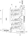
図12は、本発明の第2の実施形態に係る列並列ADC搭載固体撮像素子(CMOSイメージセンサ)の構成例を示すブロック図である。
図13は、図12の列並列ADC搭載固体撮像素子(CMOSイメージセンサ)におけるADC群をより具体的に示すブロック図である。
<2. Second Embodiment>
[Example of overall configuration of solid-state image sensor]
FIG. 12 is a block diagram illustrating a configuration example of a column parallel ADC-mounted solid-state imaging device (CMOS image sensor) according to the second embodiment of the present invention.
FIG. 13 is a block diagram showing more specifically the ADC group in the solid-state image pickup device (CMOS image sensor) equipped with the column parallel ADC of FIG.
この固体撮像素子100は、図12および図13に示すように、撮像部としての画素部110、垂直走査回路120、水平転送走査回路130、タイミング制御回路140、および画素信号読み出し部としてのAD変換装置(ADC)群150を有する。なお、画素信号読み出し部は、垂直走査回路120等を含んで構成される。
固体撮像素子100は、DA変換装置161を含むDACおよびバイアス回路160、アンプ回路(S/A)170、信号処理回路180、およびラインメモリ190を有する。
これらの構成要素のうち、画素部110、垂直走査回路120、水平転送走査回路130、ADC群150、DACおよびバイアス回路160、並びにアンプ回路(S/A)170はアナログ回路により構成される。
また、タイミング制御回路140、信号処理回路180、およびラインメモリ190はデジタル回路により構成される。
As shown in FIGS. 12 and 13, the solid-
The solid-
Among these components, the
The
画素部110は、フォトダイオードと画素内アンプとを含む画素がマトリクス状(行列状)に配置されている。
In the
図14は、本実施形態に係る4つのトランジスタで構成されるCMOSイメージセンサの画素の一例を示す図である。 FIG. 14 is a diagram illustrating an example of a pixel of a CMOS image sensor including four transistors according to the present embodiment.
この画素回路101Aは、光電変換素子としてたとえばフォトダイオード111を有している。
画素回路101Aは、この1個の光電変換素子としてのフォトダイオード111を有する。
画素回路101Aは、1個のフォトダイオード111に対し転送素子としての転送トランジスタ112、リセット素子としてのリセットトランジスタ113、増幅トランジスタ114、および選択トランジスタ115の4つのトランジスタを能動素子として有する。
The
The
The
フォトダイオード111は、入射光をその光量に応じた量の電荷(ここでは電子)に光電変換する。
転送トランジスタ112は、フォトダイオード111と出力ノードとしてのフローティングディフュージョンFD(Floating Diffusion)との間に接続されている。
転送トランジスタ112は、転送制御線LTxを通じてそのゲート(転送ゲート)に駆動信号TGが与えられることで、フォトダイオード111で光電変換された電子をフローティングディフュージョンFDに転送する。
The
The
The
リセットトランジスタ113は、電源ラインLVDDとフローティングディフュージョンFDとの間に接続されている。
リセットトランジスタ113は、リセット制御線LRSTを通してそのゲートにリセットRSTが与えられることで、フローティングディフュージョンFDの電位を電源ラインLVDDの電位にリセットする。
The
The
フローティングディフュージョンFDには、増幅トランジスタ114のゲートが接続されている。増幅トランジスタ114は、選択トランジスタ115を介して垂直信号線116に接続され、画素部外の定電流源とソースフォロアを構成している。
そして、選択制御線LSELを通して制御信号(アドレス信号またはセレクト信号)SELが選択トランジスタ115のゲートに与えられ、選択トランジスタ115がオンする。
選択トランジスタ115がオンすると、増幅トランジスタ114はフローティングディフュージョンFDの電位を増幅してその電位に応じた電圧を垂直信号線116に出力する。垂直信号線116を通じて、各画素から出力された電圧は、画素信号読み出し回路としてのADC群150に出力される。
これらの動作は、たとえば転送トランジスタ112、リセットトランジスタ113、および選択トランジスタ115の各ゲートが行単位で接続されていることから、1行分の各画素について同時に行われる。
The gate of the
Then, a control signal (address signal or select signal) SEL is applied to the gate of the
When the
These operations are performed simultaneously for each pixel for one row because, for example, the gates of the
画素部110に配線されているリセット制御線LRST、転送制御線LTx、および選択制御線LSELが一組として画素配列の各行単位で配線されている。
これらのリセット制御線LRST、転送制御線LTx、および選択制御線LSELは、画素駆動部としての垂直走査回路120により駆動される。
A reset control line LRST, a transfer control line LTx, and a selection control line LSEL wired to the
These reset control line LRST, transfer control line LTx, and selection control line LSEL are driven by a
固体撮像素子100は、画素部110の信号を順次読み出すための制御回路として内部クロックを生成するタイミング制御回路140、行アドレスや行走査を制御する垂直走査回路120、そして列アドレスや列走査を制御する水平転送走査回路130が配置される。
The solid-
タイミング制御回路140は、画素部110、垂直走査回路120、水平転送走査回路130、AD変換装置群(ADC群)150、DACおよびバイアス回路160、信号処理回路180、ラインメモリ190の信号処理に必要なタイミング信号を生成する。
The
画素部110においては、たとえばラインシャッタを使用した光子蓄積、排出により、映像や画面イメージを画素行毎に光電変換し、アナログ信号VSLをADC群に出力する。
ADC群150では、ADCブロック(各カラム部)でそれぞれ、画素部110のアナログ出力をDA変換装置(DAC)161からの参照電圧RAMPを使用したAPGA対応積分型ADC、およびデジタルCDSを行い、数ビットのデジタル信号を出力する。
In the
In the
図15は、図12および図13のDACが生成するランプ(RAMP)波形およびADCの動作タイミングの一例を示す図である。 FIG. 15 is a diagram illustrating an example of a ramp (RAMP) waveform generated by the DAC of FIGS. 12 and 13 and an operation timing of the ADC.
ADC群150は、図5に示した積分型AD変換装置10が複数列配列されている。
DAC161は、図15に示すような、階段状に変化させた傾斜するランプ波形(RAMP)である参照電圧PAMPを生成する。
各AD変換装置150Aは、比較器151、上位ビットカウンタ152、調整部153、TDC(Time-to-Digital Converter:時間量子化器)154、および論理回路155を有する。
比較器151、上位ビットカウンタ152、調整部153、TDC154の機能は図5の比較器11、上位ビットカウンタ12、調整部13、TDC14と同様の機能を有することから、ここではその詳細は省略する。
論理回路155は、上位ビットカウンタ152で生成される上位ビット(たとえば11ビット)に下位ビットTDC154で生成される下位ビット(たとえば3ビット)を追加してつなぎ合わせる。
この場合も、積分型AD変換装置150Aは、このつなぎで生ずるスパークルエラーの発生を防止することを特徴とする。
各論理回路155の出力は、水平転送線LTRFに接続されている。
そして、水平転送線LTRFに対応したk個のアンプ回路170、および信号処理回路180が配置される。
In the
DAC161, such as shown in FIG. 1 5, and generates a reference voltage PAMP is a ramp waveform which inclines varying stepwise (RAMP).
Each
The
Also in this case, the
The output of each
Then,
以上のAD変換期間終了後、水平転送走査回路130により、論理回路155によるデータが、水平転送線LTRFに転送され、アンプ回路170を経て信号処理回路180に入力され、所定の信号処理により2次元画像が生成される。
After the end of the AD conversion period, the horizontal
水平転送走査回路130では、転送速度の確保のために数チャンネル同時並列転送を行う。
タイミング制御回路140においては、画素部110、ADC群150等の各ブロックでの信号処理に必要なタイミングが生成される。
後段の信号処理回路180では、ラインメモリ190内に格納された信号より縦線欠陥や点欠陥の補正、信号のクランプを行ったり、パラレル-シリアル変換、圧縮、符号化、加算、平均、間欠動作などデジタル信号処理を行う。
ラインメモリ190には、画素行毎に送信されるデジタル信号が格納される。
本実施形態の固体撮像素子100においては、信号処理回路180のデジタル出力がISPやベースバンド(basEBand)LSIの入力として送信される。
The horizontal
In the
In the subsequent
The
In the solid-
次に、上記構成による動作を説明する。 Next, the operation according to the above configuration will be described.
DAC161において、参照電圧PAMPが生成される。
各AD変換装置150Aにおいて、垂直信号線116に読み出されたアナログ信号電位VSLが列毎に配置された比較器151で階段状に変化する参照電圧RAMPと比較される。
比較器151からは、比較結果に応じたレベルの信号VCOが調整部153およびTDC154に出力される。
調整部153においては、比較器151の出力信号VCOと主クロック信号CLKAの同期化が行われる。そして、調整部153では、同期化を行った結果の信号を用いて、上位ビットカウンタ152の動作開始および停止のタイミングと、主クロック信号CLKAの位相情報をラッチする値が決定される。
具体的には、調整部153においては、比較器151の出力信号VCOを主クロック信号CLKAの立ち上がりと立ち下がりの両エッジで同期化され、この同期化信号がカウント動作開始信号VCO_SYNCとして出力される。
また、調整部153においては、カウント動作開始信号VCO_SYNCを基に主クロック信号CLKAの位相情報をラッチするラッチタイミング信号VCO_SYNCDが生成される。生成されたラッチタイミング信号VCO_SYNCDはTDC154に供給される。
上位ビットカウンタ152においては、基本的に、比較器151の出力信号VCOが反転したことをトリガとして動作開始もしくは動作停止し、主クロック信号CLKAの周期ごとに計数される。
上位ビットカウンタ152では、調整部153により比較器151の出力信号VCOと主クロックCLKAと同期させて生成されたカウント動作開始信号VCO_SYNCをトリガとして、調整部153を介した主クロック信号CLKAOの周期ごとに計数される。
TDC14では、位相の異なる主クロックCLKAを含む複数のクロック信号CLKA〜CLKDを用いて比較器151の出力信号VCOが反転したタイミングで位相情報がラッチされる。そして、TDC154では、ラッチした値がデコードされて、クロック周期より分解能が高い下位ビットが出力される。
そして、論理回路155において、上位ビットカウンタ152で生成される上位ビット(たとえば11ビット)に下位ビットTDC154で生成される下位ビット(たとえば3ビット)が追加されてつなぎ合わされる。
この場合、積分型AD変換装置150Aでは、このつなぎで生ずるスパークルエラーの発生が防止される。
これにより、AD変換が完了する。
デジタル信号に変換された信号は、たとえば水平(列)転送走査回路130により、順番に水平転送線LTRFを介してアンプ回路170に読み出され、最終的に出力される。
このようにして、列並列出力処理が行われる。
In the DAC 161, a reference voltage PAMP is generated.
In each
From the
In the
Specifically, in
Further, the
The upper bit counter 152 basically starts or stops operating when the output signal VCO of the
The higher-order bit counter 152 uses the count operation start signal VCO_SYNC generated by the
In the
Then, in the
In this case, in the integral
Thereby, AD conversion is completed.
The signals converted into digital signals are sequentially read out, for example, by the horizontal (column)
In this way, column parallel output processing is performed.
本第2の実施形態に係る固体撮像素子はであるCMOSイメージセンサ100は図5のAD変換装置(ADC)10を適用した。
したがって、本固体撮像素子によれば、上位ビットと下位ビットのつなぎで生ずるスパークルエラーを原理的に防止することで、AD変換装置のINL・DNL特性を向上させることができる。
また、同期化回路は、一般的な高速クロック、低速クロックを共用して消費電力を削減するADカウンタに搭載されており、ハードウェアの増加がほとんどない。
The
Therefore, according to the present solid-state imaging device, it is possible to improve the INL / DNL characteristics of the AD converter by preventing in principle a sparkle error that occurs between the upper bits and the lower bits.
The synchronization circuit is mounted on an AD counter that reduces power consumption by sharing a common high-speed clock and low-speed clock, and there is almost no increase in hardware.
このような効果を有する固体撮像素子は、デジタルカメラやビデオカメラの撮像デバイスとして適用することができる。 A solid-state imaging device having such an effect can be applied as an imaging device for a digital camera or a video camera.
<3.第3の実施形態>
[カメラシステムの構成例]
図16は、本発明の実施形態に係る固体撮像素子が適用されるカメラシステムの構成の一例を示す図である。
<3. Third Embodiment>
[Example of camera system configuration]
FIG. 16 is a diagram illustrating an example of a configuration of a camera system to which the solid-state imaging device according to the embodiment of the present invention is applied.
本カメラシステム200は、図16に示すように、本実施形態に係る固体撮像素子100が適用可能な撮像デバイス210を有する。
カメラシステム200は、撮像デバイス210の画素領域に入射光を導く(被写体像を結像する)光学系として、たとえば入射光(像光)を撮像面上に結像させるレンズ220を有する。
さらに、カメラシステム200は、撮像デバイス210を駆動する駆動回路(DRV)230と、撮像デバイス210の出力信号を処理する信号処理回路(PRC)240と、を有する。
As shown in FIG. 16, the
The
The
駆動回路230は、撮像デバイス210内の回路を駆動するスタートパルスやクロックパルスを含む各種のタイミング信号を生成するタイミングジェネレータ(図示せず)を有し、所定のタイミング信号で撮像デバイス210を駆動する。
The
また、信号処理回路240は、撮像デバイス210の出力信号に対して所定の信号処理を施す。
信号処理回路240で処理された画像信号は、たとえばメモリなどの記録媒体に記録される。記録媒体に記録された画像情報は、プリンタなどによってハードコピーされる。また、信号処理回路240で処理された画像信号を液晶ディスプレイ等からなるモニターに動画として映し出される。
The
The image signal processed by the
上述したように、デジタルスチルカメラ等の撮像装置において、撮像デバイス210として、先述した固体撮像素子100を搭載することで、高精度なカメラが実現できる。
As described above, a high-precision camera can be realized by mounting the above-described solid-
10・・・AD変換装置、11・・比較器、12・・・上位ビットカウンタ、13・・・調整部、131・・・同期化回路、132・・・遅延部、14・・・TDC(Time-to-Digital Converter:時間量子化器)、141〜143・・・FF(第1のラッチ)、144・・・FF(第2のラッチ)、15・・・転送バス、100・・・固体撮像素子、110・・・画素部、120・・・垂直走査回路、130・・・水平転送走査回路、140・・・タイミング制御回路、141・・・パルス生成部、150・・・カラム処理回路群(ADC群)、151・・・比較器、152・・・カウンタ、153・・・ラッチ(メモリ)、161・・・DA変換装置(DAC)、170・・・アンプ回路、180・・・信号処理回路、190・・・ラインメモリ、LTRF・・・水平転送線、200・・・カメラシステム、210・・・撮像デバイス、220・・・レンズ、230・・・駆動回路、240・・・信号処理回路。
DESCRIPTION OF
Claims (7)
前記比較器の出力信号が反転したことをトリガとして動作開始または動作停止し、主クロック信号の周期ごとに計数する上位ビットカウンタと、
位相の異なる前記主クロックを含む複数のクロック信号を用いて前記比較器の出力信号が反転したタイミングで位相情報をラッチし、当該ラッチした値をデコードすることでクロック周期より分解能が高い下位ビットを出力する時間量子化器と、
前記比較器の出力信号と前記主クロック信号の同期化を行い、同期化を行った結果の信号を用いて、上位ビットカウンタの動作開始および停止のタイミングと、前記主クロック信号の位相情報をラッチする値を決定する調整部と
を有する積分型AD変換装置。 A comparator that compares the input voltage with the reference voltage of the ramp waveform whose voltage value changes linearly with time;
An upper bit counter that starts or stops operation triggered by the inversion of the output signal of the comparator, and counts every period of the main clock signal;
The phase information is latched at the timing when the output signal of the comparator is inverted using a plurality of clock signals including the main clock having different phases, and the latched value is decoded to obtain lower bits having a resolution higher than the clock cycle. An output time quantizer;
The output signal of the comparator and the main clock signal are synchronized, and the timing of the start and stop of the upper bit counter and the phase information of the main clock signal are latched using the signal resulting from the synchronization And an adjustment type AD converter that determines a value to be determined.
前記比較器の出力信号を前記主クロック信号の立ち上がりと立ち下がりの両エッジで同期化し、当該同期化信号をカウント動作開始信号として出力する同期化回路を含み、
前記カウント動作開始信号を基に前記主クロック信号の位相情報をラッチするラッチタイミング信号を生成し、当該ラッチタイミング信号を前記時間量子化器に出力し、
前記上位ビットカウンタは、
前記カウント動作開始信号をトリガとして計数動作を開始する
請求項1記載の積分型AD変換装置。 The adjustment unit is
A synchronization circuit for synchronizing the output signal of the comparator at both rising and falling edges of the main clock signal and outputting the synchronization signal as a count operation start signal;
Generating a latch timing signal for latching phase information of the main clock signal based on the count operation start signal, and outputting the latch timing signal to the time quantizer;
The upper bit counter is
The integral AD converter according to claim 1, wherein the counting operation is started by using the counting operation start signal as a trigger.
前記主クロックを含む複数のクロック信号のうち、当該主クロック信号を除くクロック信号の位相情報を前記比較器の出力信号に同期してラッチする少なくとも一つの第1のラッチと、
前記主クロックの位相情報を前記ラッチタイミング信号に同期してラッチする第2のラッチと、を含む
請求項2記載の積分型AD変換装置。 The time quantizer is
At least one first latch that latches phase information of a clock signal excluding the main clock signal among a plurality of clock signals including the main clock in synchronization with an output signal of the comparator;
The integral AD converter according to claim 2, further comprising: a second latch that latches phase information of the main clock in synchronization with the latch timing signal.
請求項3記載の積分型AD変換装置。 The integral AD converter according to claim 3, wherein the second latch outputs a value inverted from the logic of the main clock signal.
前記カウント動作開始信号を遅延させて前記ラッチタイミング信号を生成し、当該ラッチタイミング信号を前記時間量子化器に出力する遅延部を含む
請求項2から4のいずれか一に記載の積分型AD変換装置。 The adjustment unit is
5. The integral AD conversion according to claim 2, further comprising: a delay unit that delays the count operation start signal to generate the latch timing signal and outputs the latch timing signal to the time quantizer. apparatus.
前記画素部から複数の画素単位で画素信号の読み出しを行う画素信号読み出し部と、を有し、
前記画素信号読み出し部は、
画素の列配列に対応して、読み出したアナログ信号をデジタル信号に変換する積分型アナログデジタル(AD)変換装置を有し、
前記積分型AD変換装置は、
ランプ波である参照電圧が供給され、供給された参照電圧と当該列の画素の読み出しアナログ信号電位とを比較する複数の比較器と、
時間とともに電圧値が線形に変化するランプ波形の参照電圧と該列の画素の読み出しアナログ信号電位とを比較する比較器と、
前記比較器の出力信号が反転したことをトリガとして動作開始または動作停止し、主クロック信号の周期ごとに計数する上位ビットカウンタと、
位相の異なる前記主クロックを含む複数のクロック信号を用いて前記比較器の出力信号が反転したタイミングで位相情報をラッチし、当該ラッチした値をデコードすることでクロック周期より分解能が高い下位ビットを出力する時間量子化器と、
前記比較器の出力信号と前記主クロック信号の同期化を行い、同期化を行った結果の信号を用いて、上位ビットカウンタの動作開始および停止のタイミングと、前記主クロック信号の位相情報をラッチする値を決定する調整部と、を含む
固体撮像素子。 A pixel unit in which a plurality of pixels that perform photoelectric conversion are arranged in a matrix;
A pixel signal readout unit that reads out pixel signals from the pixel unit in units of a plurality of pixels,
The pixel signal readout unit includes:
Corresponding to the column arrangement of pixels, it has an integral analog-digital (AD) conversion device that converts the read analog signal into a digital signal,
The integral AD converter is
A reference voltage that is a ramp wave is supplied, and a plurality of comparators that compare the supplied reference voltage with the readout analog signal potential of the pixel in the column,
A comparator that compares the reference voltage of the ramp waveform whose voltage value linearly changes with time and the readout analog signal potential of the pixels in the column;
An upper bit counter that starts or stops operation triggered by the inversion of the output signal of the comparator, and counts every period of the main clock signal;
The phase information is latched at the timing when the output signal of the comparator is inverted using a plurality of clock signals including the main clock having different phases, and the latched value is decoded to obtain lower bits having a resolution higher than the clock cycle. An output time quantizer;
The have line synchronization of the comparator output signal and said main clock signal by using a signal of a result of the synchronization, the timing of operation start and stop of the upper bit counter, the phase information of the main clock signal A solid-state imaging device including an adjustment unit that determines a value to be latched.
前記固体撮像素子に被写体像を結像する光学系と、を有し、
前記固体撮像素子は、
光電変換を行う複数の画素が行列状に配列された画素部と、
前記画素部から複数の画素単位で画素信号の読み出しを行う画素信号読み出し部と、を有し、
前記画素信号読み出し部は、
画素の列配列に対応して、読み出したアナログ信号をデジタル信号に変換する積分型アナログデジタル(AD)変換装置を有し、
前記積分型AD変換装置は、
ランプ波である参照電圧が供給され、供給された参照電圧と当該列の画素の読み出しアナログ信号電位とを比較する複数の比較器と、
時間とともに電圧値が線形に変化するランプ波形の参照電圧と該列の画素の読み出しアナログ信号電位とを比較する比較器と、
前記比較器の出力信号が反転したことをトリガとして動作開始または動作停止し、主クロック信号の周期ごとに計数する上位ビットカウンタと、
位相の異なる前記主クロックを含む複数のクロック信号を用いて前記比較器の出力信号が反転したタイミングで位相情報をラッチし、当該ラッチした値をデコードすることでクロック周期より分解能が高い下位ビットを出力する時間量子化器と、
前記比較器の出力信号と前記主クロック信号の同期化を行い、同期化を行った結果の信号を用いて、上位ビットカウンタの動作開始および停止のタイミングと、前記主クロック信号の位相情報をラッチする値を決定する調整部と、を含む
カメラシステム。 A solid-state image sensor;
An optical system that forms a subject image on the solid-state imaging device,
The solid-state imaging device is
A pixel unit in which a plurality of pixels that perform photoelectric conversion are arranged in a matrix;
A pixel signal readout unit that reads out pixel signals from the pixel unit in units of a plurality of pixels,
The pixel signal readout unit includes:
Corresponding to the column arrangement of pixels, it has an integral analog-digital (AD) conversion device that converts the read analog signal into a digital signal,
The integral AD converter is
A reference voltage that is a ramp wave is supplied, and a plurality of comparators that compare the supplied reference voltage with the readout analog signal potential of the pixel in the column,
A comparator that compares the reference voltage of the ramp waveform whose voltage value linearly changes with time and the readout analog signal potential of the pixels in the column;
An upper bit counter that starts or stops operation triggered by the inversion of the output signal of the comparator, and counts every period of the main clock signal;
The phase information is latched at the timing when the output signal of the comparator is inverted using a plurality of clock signals including the main clock having different phases, and the latched value is decoded to obtain lower bits having a resolution higher than the clock cycle. An output time quantizer;
The have line synchronization of the comparator output signal and said main clock signal by using a signal of a result of the synchronization, the timing of operation start and stop of the upper bit counter, the phase information of the main clock signal An adjustment unit for determining a value to be latched, and a camera system.
Priority Applications (3)
| Application Number | Priority Date | Filing Date | Title |
|---|---|---|---|
| JP2009107105A JP5407523B2 (en) | 2009-04-24 | 2009-04-24 | Integrating AD converter, solid-state imaging device, and camera system |
| US12/659,585 US8456554B2 (en) | 2009-04-24 | 2010-03-15 | Integrated AD converter, solid state imaging device, and camera system |
| CN2010101486856A CN101873136B (en) | 2009-04-24 | 2010-04-16 | Integrated AD converter, solid state imaging device, and camera system |
Applications Claiming Priority (1)
| Application Number | Priority Date | Filing Date | Title |
|---|---|---|---|
| JP2009107105A JP5407523B2 (en) | 2009-04-24 | 2009-04-24 | Integrating AD converter, solid-state imaging device, and camera system |
Publications (2)
| Publication Number | Publication Date |
|---|---|
| JP2010258817A JP2010258817A (en) | 2010-11-11 |
| JP5407523B2 true JP5407523B2 (en) | 2014-02-05 |
Family
ID=42991808
Family Applications (1)
| Application Number | Title | Priority Date | Filing Date |
|---|---|---|---|
| JP2009107105A Active JP5407523B2 (en) | 2009-04-24 | 2009-04-24 | Integrating AD converter, solid-state imaging device, and camera system |
Country Status (3)
| Country | Link |
|---|---|
| US (1) | US8456554B2 (en) |
| JP (1) | JP5407523B2 (en) |
| CN (1) | CN101873136B (en) |
Families Citing this family (47)
| Publication number | Priority date | Publication date | Assignee | Title |
|---|---|---|---|---|
| JP5375277B2 (en) * | 2009-04-02 | 2013-12-25 | ソニー株式会社 | Solid-state imaging device, imaging device, electronic device, AD conversion device, AD conversion method |
| JP5372667B2 (en) * | 2009-09-01 | 2013-12-18 | オリンパス株式会社 | AD converter and solid-state imaging device |
| JP5540901B2 (en) * | 2010-06-01 | 2014-07-02 | ソニー株式会社 | Integrating A / D Converter, Integrating A / D Conversion Method, Solid-State Image Sensor, and Camera System |
| US20120154653A1 (en) * | 2010-12-20 | 2012-06-21 | Compton John T | Suspending column addressing in image sensors |
| JP5695401B2 (en) * | 2010-12-01 | 2015-04-08 | オリンパス株式会社 | Imaging device |
| JP2012191359A (en) * | 2011-03-09 | 2012-10-04 | Sony Corp | A/d conversion device, a/d conversion method and program |
| JP5881512B2 (en) * | 2011-04-11 | 2016-03-09 | オリンパス株式会社 | Clock generation circuit and imaging apparatus |
| JP5749579B2 (en) * | 2011-06-14 | 2015-07-15 | オリンパス株式会社 | AD conversion circuit and solid-state imaging device |
| CN103108137B (en) * | 2011-11-14 | 2017-04-12 | 豪威科技股份有限公司 | Common terminal of image sensor system used for transmitting clock signals and control signals |
| US8890945B2 (en) | 2011-11-14 | 2014-11-18 | Omnivision Technologies, Inc. | Shared terminal of an image sensor system for transferring image data and control signals |
| CN103108143B (en) * | 2011-11-14 | 2016-12-21 | 豪威科技股份有限公司 | Image sensor system for transmitted image data and the shared terminal of control signal |
| JP6195161B2 (en) * | 2012-02-17 | 2017-09-13 | 国立大学法人北海道大学 | Integrating AD converter and CMOS image sensor |
| KR101921964B1 (en) | 2012-03-05 | 2019-02-13 | 삼성전자주식회사 | Line Memory and CMOS Image IC Device |
| JP5904899B2 (en) * | 2012-08-06 | 2016-04-20 | オリンパス株式会社 | Imaging device |
| JP5977634B2 (en) * | 2012-09-24 | 2016-08-24 | オリンパス株式会社 | Data processing circuit and solid-state imaging device |
| JP5973321B2 (en) * | 2012-10-30 | 2016-08-23 | ルネサスエレクトロニクス株式会社 | Solid-state image sensor |
| JP5953225B2 (en) * | 2012-12-27 | 2016-07-20 | オリンパス株式会社 | AD conversion circuit and solid-state imaging device |
| US8786474B1 (en) * | 2013-03-15 | 2014-07-22 | Kabushiki Kaisha Toshiba | Apparatus for programmable metastable ring oscillator period for multiple-hit delay-chain based time-to-digital circuits |
| US9063520B2 (en) * | 2013-03-15 | 2015-06-23 | Kabushiki Kaisha Toshiba | Apparatus for inserting delay, nuclear medicine imaging apparatus, method for inserting delay, and method of calibration |
| KR102135684B1 (en) | 2013-07-24 | 2020-07-20 | 삼성전자주식회사 | Counter circuit, ADC and Image sensor incluing the same and method of correlated double sampling |
| JP5767287B2 (en) * | 2013-09-13 | 2015-08-19 | オリンパス株式会社 | Imaging device |
| JP6273126B2 (en) * | 2013-11-14 | 2018-01-31 | キヤノン株式会社 | AD converter, solid-state imaging device, and imaging system |
| JP6394056B2 (en) * | 2013-11-27 | 2018-09-26 | ソニー株式会社 | A / D conversion device, gray code generation device, imaging device, and electronic device |
| KR102292644B1 (en) * | 2013-12-24 | 2021-08-23 | 삼성전자주식회사 | Image sensor for operating with high speed |
| JP6274898B2 (en) | 2014-02-17 | 2018-02-07 | キヤノン株式会社 | Solid-state imaging device and camera |
| JP6341688B2 (en) * | 2014-02-25 | 2018-06-13 | キヤノン株式会社 | Solid-state imaging device and imaging system |
| WO2016021413A1 (en) * | 2014-08-06 | 2016-02-11 | ソニー株式会社 | Solid-state image pickup element and solid-state image pickup device |
| JP2016213549A (en) * | 2015-04-30 | 2016-12-15 | 国立大学法人北海道大学 | Digital circuit, A / D (Analog / Digital) conversion circuit, and digital signal processing method |
| JP6801963B2 (en) * | 2016-01-08 | 2020-12-16 | 国立大学法人北海道大学 | A / D (Analog / Digital) conversion circuit and A / D conversion method |
| US9842645B2 (en) | 2016-04-08 | 2017-12-12 | Panasonic Intellectual Property Management Co., Ltd. | Nonvolatile memory device including nonvolatile memory and resistance-time converter, and integrated circuit card including nonvolatile memory device |
| CN106303313B (en) * | 2016-08-12 | 2019-04-30 | 中国科学院上海高等研究院 | Quantization Summation Circuit of Compressed Sensing CMOS Image Sensor |
| EP3339985B1 (en) * | 2016-12-22 | 2019-05-08 | ams AG | Time-to-digital converter and conversion method |
| US10931908B2 (en) * | 2017-03-08 | 2021-02-23 | Panasonic Semiconductor Solutions Co., Ltd. | Solid-state imaging device, and camera system using same |
| JP7214622B2 (en) * | 2017-03-08 | 2023-01-30 | ヌヴォトンテクノロジージャパン株式会社 | Solid-state imaging device and camera system using the same |
| WO2019046581A1 (en) * | 2017-08-30 | 2019-03-07 | Massachusetts Institute Of Technology | Dual-mode imaging receiver |
| US10367519B2 (en) * | 2017-10-11 | 2019-07-30 | Tech Idea Co., Ltd. | Time domain A/D converter group and sensor device using the same |
| JP6941890B2 (en) * | 2017-10-11 | 2021-09-29 | 株式会社テックイデア | Time domain A / D converter group and sensor device using this |
| US11153514B2 (en) * | 2017-11-30 | 2021-10-19 | Brillnics Singapore Pte. Ltd. | Solid-state imaging device, method for driving solid-state imaging device, and electronic apparatus |
| KR102443224B1 (en) * | 2017-12-14 | 2022-09-15 | 삼성전자주식회사 | Quantizer including capacitors and operating method of quantizer |
| CN108551344B (en) * | 2018-03-29 | 2022-04-01 | 上海集成电路研发中心有限公司 | Double-sampling analog-to-digital conversion circuit |
| EP3595292B1 (en) * | 2018-07-13 | 2021-06-23 | Teledyne Dalsa B.V. | Image sensor system |
| DE102018220688A1 (en) * | 2018-11-30 | 2020-06-04 | Ibeo Automotive Systems GmbH | Analog-to-digital converter |
| KR102856356B1 (en) * | 2019-10-21 | 2025-09-04 | 삼성전자주식회사 | Analog digital converter including delay circuit and compensator, image sensor including the same, and operating method thereof |
| US11575853B2 (en) * | 2020-09-29 | 2023-02-07 | Shenzhen GOODIX Technology Co., Ltd. | Image sensor having high resolution analog to digital converter |
| CN114859341B (en) * | 2021-02-03 | 2023-05-05 | 上海禾赛科技有限公司 | Synchronous circuit, data processing chip and radar |
| US11329652B1 (en) * | 2021-03-04 | 2022-05-10 | Shenzhen GOODIX Technology Co., Ltd. | Loadable true-single-phase-clocking flop-based counter |
| US12063046B2 (en) * | 2022-12-09 | 2024-08-13 | Allegro Microsystems, Llc | Oscillator monitoring circuits for different oscillator domains |
Family Cites Families (11)
| Publication number | Priority date | Publication date | Assignee | Title |
|---|---|---|---|---|
| JPH11341337A (en) * | 1998-05-22 | 1999-12-10 | Canon Inc | Signal processing device, imaging system, and phase synchronization method |
| JPH11355645A (en) * | 1998-06-09 | 1999-12-24 | Canon Inc | Head-separated imaging system |
| JP4289206B2 (en) * | 2004-04-26 | 2009-07-01 | ソニー株式会社 | Counter circuit |
| JP2006020171A (en) * | 2004-07-02 | 2006-01-19 | Fujitsu Ltd | Differential comparator, analog / digital converter, imaging device |
| WO2007054902A1 (en) * | 2005-11-11 | 2007-05-18 | Nxp B.V. | Integrating analog to digital converter |
| KR100955637B1 (en) * | 2005-12-27 | 2010-05-06 | 후지쯔 마이크로일렉트로닉스 가부시키가이샤 | Solid-state image pickup device and dark current component removal method |
| KR100826513B1 (en) * | 2006-09-08 | 2008-05-02 | 삼성전자주식회사 | CDS and ADC apparatus and method using multiple sampling |
| JP2008092091A (en) * | 2006-09-29 | 2008-04-17 | Tokyo Institute Of Technology | Integrating A / D Converter, Imaging Device Having A / D Converter, and Electronic Device |
| JP2008306695A (en) * | 2007-05-10 | 2008-12-18 | Sony Corp | Data transfer circuit, solid-state imaging device, and camera system |
| JP4953970B2 (en) * | 2007-08-03 | 2012-06-13 | パナソニック株式会社 | Physical quantity detection device and driving method thereof |
| JP4389981B2 (en) * | 2007-08-06 | 2009-12-24 | ソニー株式会社 | Solid-state imaging device, analog-digital conversion method of solid-state imaging device, and imaging device |
-
2009
- 2009-04-24 JP JP2009107105A patent/JP5407523B2/en active Active
-
2010
- 2010-03-15 US US12/659,585 patent/US8456554B2/en active Active
- 2010-04-16 CN CN2010101486856A patent/CN101873136B/en active Active
Also Published As
| Publication number | Publication date |
|---|---|
| US20100271525A1 (en) | 2010-10-28 |
| CN101873136B (en) | 2013-07-24 |
| US8456554B2 (en) | 2013-06-04 |
| CN101873136A (en) | 2010-10-27 |
| JP2010258817A (en) | 2010-11-11 |
Similar Documents
| Publication | Publication Date | Title |
|---|---|---|
| JP5407523B2 (en) | Integrating AD converter, solid-state imaging device, and camera system | |
| US8358349B2 (en) | A/D converter, solid-state imaging device and camera system | |
| JP5728826B2 (en) | Column A / D converter, column A / D conversion method, solid-state imaging device, and camera system | |
| US9204070B2 (en) | Integrating A/D converter, integrating A/D conversion method, solid-state imaging device and camera system | |
| JP5359521B2 (en) | Binary value conversion circuit and method, AD conversion apparatus, solid-state imaging device, and camera system | |
| JP5531797B2 (en) | Solid-state imaging device and camera system | |
| JP5799531B2 (en) | A / D converter, A / D conversion method, solid-state imaging device, and camera system | |
| US7859583B2 (en) | Solid-state image capture device, analog/digital conversion method for solid state image capture device, and image capture device | |
| JP2010251957A (en) | AD converter, solid-state imaging device, and camera system | |
| JP2011166197A (en) | Signal transmission circuit, column a/d converter, solid-state imaging element, and camera system |
Legal Events
| Date | Code | Title | Description |
|---|---|---|---|
| A621 | Written request for application examination |
Free format text: JAPANESE INTERMEDIATE CODE: A621 Effective date: 20120312 |
|
| A977 | Report on retrieval |
Free format text: JAPANESE INTERMEDIATE CODE: A971007 Effective date: 20130405 |
|
| A131 | Notification of reasons for refusal |
Free format text: JAPANESE INTERMEDIATE CODE: A131 Effective date: 20130409 |
|
| A521 | Request for written amendment filed |
Free format text: JAPANESE INTERMEDIATE CODE: A523 Effective date: 20130603 |
|
| A131 | Notification of reasons for refusal |
Free format text: JAPANESE INTERMEDIATE CODE: A131 Effective date: 20130625 |
|
| A521 | Request for written amendment filed |
Free format text: JAPANESE INTERMEDIATE CODE: A523 Effective date: 20130819 |
|
| TRDD | Decision of grant or rejection written | ||
| A01 | Written decision to grant a patent or to grant a registration (utility model) |
Free format text: JAPANESE INTERMEDIATE CODE: A01 Effective date: 20131008 |
|
| A61 | First payment of annual fees (during grant procedure) |
Free format text: JAPANESE INTERMEDIATE CODE: A61 Effective date: 20131021 |
|
| R151 | Written notification of patent or utility model registration |
Ref document number: 5407523 Country of ref document: JP Free format text: JAPANESE INTERMEDIATE CODE: R151 |
|
| R250 | Receipt of annual fees |
Free format text: JAPANESE INTERMEDIATE CODE: R250 |
|
| R250 | Receipt of annual fees |
Free format text: JAPANESE INTERMEDIATE CODE: R250 |
|
| R250 | Receipt of annual fees |
Free format text: JAPANESE INTERMEDIATE CODE: R250 |
|
| R250 | Receipt of annual fees |
Free format text: JAPANESE INTERMEDIATE CODE: R250 |
|
| R250 | Receipt of annual fees |
Free format text: JAPANESE INTERMEDIATE CODE: R250 |