JP5380037B2 - Method for manufacturing semiconductor device - Google Patents
Method for manufacturing semiconductor device Download PDFInfo
- Publication number
- JP5380037B2 JP5380037B2 JP2008269324A JP2008269324A JP5380037B2 JP 5380037 B2 JP5380037 B2 JP 5380037B2 JP 2008269324 A JP2008269324 A JP 2008269324A JP 2008269324 A JP2008269324 A JP 2008269324A JP 5380037 B2 JP5380037 B2 JP 5380037B2
- Authority
- JP
- Japan
- Prior art keywords
- photoresist
- film
- semiconductor layer
- forming
- amorphous silicon
- Prior art date
- Legal status (The legal status is an assumption and is not a legal conclusion. Google has not performed a legal analysis and makes no representation as to the accuracy of the status listed.)
- Expired - Fee Related
Links
- 238000000034 method Methods 0.000 title claims description 68
- 239000004065 semiconductor Substances 0.000 title claims description 67
- 238000004519 manufacturing process Methods 0.000 title claims description 31
- 229920002120 photoresistant polymer Polymers 0.000 claims description 124
- 229910021417 amorphous silicon Inorganic materials 0.000 claims description 54
- 239000000758 substrate Substances 0.000 claims description 37
- 229910052751 metal Inorganic materials 0.000 claims description 32
- 239000002184 metal Substances 0.000 claims description 32
- 230000001681 protective effect Effects 0.000 claims description 19
- 238000005530 etching Methods 0.000 claims description 14
- 238000004380 ashing Methods 0.000 claims description 9
- 239000012535 impurity Substances 0.000 claims description 9
- 239000010408 film Substances 0.000 description 118
- 239000010410 layer Substances 0.000 description 80
- 238000000206 photolithography Methods 0.000 description 12
- 239000011521 glass Substances 0.000 description 11
- 239000000463 material Substances 0.000 description 9
- 238000007687 exposure technique Methods 0.000 description 7
- 239000010936 titanium Substances 0.000 description 6
- 229910052581 Si3N4 Inorganic materials 0.000 description 5
- RTAQQCXQSZGOHL-UHFFFAOYSA-N Titanium Chemical compound [Ti] RTAQQCXQSZGOHL-UHFFFAOYSA-N 0.000 description 5
- 239000011651 chromium Substances 0.000 description 5
- 239000010949 copper Substances 0.000 description 5
- 239000004973 liquid crystal related substance Substances 0.000 description 5
- 239000011159 matrix material Substances 0.000 description 5
- HQVNEWCFYHHQES-UHFFFAOYSA-N silicon nitride Chemical compound N12[Si]34N5[Si]62N3[Si]51N64 HQVNEWCFYHHQES-UHFFFAOYSA-N 0.000 description 5
- 229910052719 titanium Inorganic materials 0.000 description 5
- IJGRMHOSHXDMSA-UHFFFAOYSA-N Atomic nitrogen Chemical compound N#N IJGRMHOSHXDMSA-UHFFFAOYSA-N 0.000 description 4
- VYZAMTAEIAYCRO-UHFFFAOYSA-N Chromium Chemical compound [Cr] VYZAMTAEIAYCRO-UHFFFAOYSA-N 0.000 description 4
- RYGMFSIKBFXOCR-UHFFFAOYSA-N Copper Chemical compound [Cu] RYGMFSIKBFXOCR-UHFFFAOYSA-N 0.000 description 4
- 229910052782 aluminium Inorganic materials 0.000 description 4
- XAGFODPZIPBFFR-UHFFFAOYSA-N aluminium Chemical compound [Al] XAGFODPZIPBFFR-UHFFFAOYSA-N 0.000 description 4
- 229910052804 chromium Inorganic materials 0.000 description 4
- 229910052802 copper Inorganic materials 0.000 description 4
- VYPSYNLAJGMNEJ-UHFFFAOYSA-N silicon dioxide Inorganic materials O=[Si]=O VYPSYNLAJGMNEJ-UHFFFAOYSA-N 0.000 description 4
- 239000010409 thin film Substances 0.000 description 4
- ZOKXTWBITQBERF-UHFFFAOYSA-N Molybdenum Chemical compound [Mo] ZOKXTWBITQBERF-UHFFFAOYSA-N 0.000 description 3
- 229910052779 Neodymium Inorganic materials 0.000 description 3
- 239000000956 alloy Substances 0.000 description 3
- 229910045601 alloy Inorganic materials 0.000 description 3
- 238000005229 chemical vapour deposition Methods 0.000 description 3
- 239000004020 conductor Substances 0.000 description 3
- 238000010438 heat treatment Methods 0.000 description 3
- 229910052750 molybdenum Inorganic materials 0.000 description 3
- 239000011733 molybdenum Substances 0.000 description 3
- QEFYFXOXNSNQGX-UHFFFAOYSA-N neodymium atom Chemical compound [Nd] QEFYFXOXNSNQGX-UHFFFAOYSA-N 0.000 description 3
- 229910052814 silicon oxide Inorganic materials 0.000 description 3
- WFKWXMTUELFFGS-UHFFFAOYSA-N tungsten Chemical compound [W] WFKWXMTUELFFGS-UHFFFAOYSA-N 0.000 description 3
- 229910052721 tungsten Inorganic materials 0.000 description 3
- 239000010937 tungsten Substances 0.000 description 3
- XUIMIQQOPSSXEZ-UHFFFAOYSA-N Silicon Chemical compound [Si] XUIMIQQOPSSXEZ-UHFFFAOYSA-N 0.000 description 2
- XLOMVQKBTHCTTD-UHFFFAOYSA-N Zinc monoxide Chemical compound [Zn]=O XLOMVQKBTHCTTD-UHFFFAOYSA-N 0.000 description 2
- 230000015556 catabolic process Effects 0.000 description 2
- 230000001413 cellular effect Effects 0.000 description 2
- 229910052736 halogen Inorganic materials 0.000 description 2
- 150000002367 halogens Chemical class 0.000 description 2
- 229910052739 hydrogen Inorganic materials 0.000 description 2
- 239000001257 hydrogen Substances 0.000 description 2
- 150000002431 hydrogen Chemical class 0.000 description 2
- AMGQUBHHOARCQH-UHFFFAOYSA-N indium;oxotin Chemical compound [In].[Sn]=O AMGQUBHHOARCQH-UHFFFAOYSA-N 0.000 description 2
- 229910052757 nitrogen Inorganic materials 0.000 description 2
- 238000002161 passivation Methods 0.000 description 2
- 238000000059 patterning Methods 0.000 description 2
- 230000002093 peripheral effect Effects 0.000 description 2
- 229910052710 silicon Inorganic materials 0.000 description 2
- 239000010703 silicon Substances 0.000 description 2
- 239000002356 single layer Substances 0.000 description 2
- 125000006850 spacer group Chemical group 0.000 description 2
- 238000004544 sputter deposition Methods 0.000 description 2
- 239000000126 substance Substances 0.000 description 2
- 229910052715 tantalum Inorganic materials 0.000 description 2
- GUVRBAGPIYLISA-UHFFFAOYSA-N tantalum atom Chemical compound [Ta] GUVRBAGPIYLISA-UHFFFAOYSA-N 0.000 description 2
- OAICVXFJPJFONN-UHFFFAOYSA-N Phosphorus Chemical compound [P] OAICVXFJPJFONN-UHFFFAOYSA-N 0.000 description 1
- 239000000853 adhesive Substances 0.000 description 1
- 230000001070 adhesive effect Effects 0.000 description 1
- 239000005407 aluminoborosilicate glass Substances 0.000 description 1
- 229910052788 barium Inorganic materials 0.000 description 1
- DSAJWYNOEDNPEQ-UHFFFAOYSA-N barium atom Chemical compound [Ba] DSAJWYNOEDNPEQ-UHFFFAOYSA-N 0.000 description 1
- 230000015572 biosynthetic process Effects 0.000 description 1
- 239000005388 borosilicate glass Substances 0.000 description 1
- 238000004140 cleaning Methods 0.000 description 1
- 239000011248 coating agent Substances 0.000 description 1
- 238000000576 coating method Methods 0.000 description 1
- 150000001875 compounds Chemical class 0.000 description 1
- 238000011109 contamination Methods 0.000 description 1
- 239000013078 crystal Substances 0.000 description 1
- 238000010586 diagram Methods 0.000 description 1
- 230000000694 effects Effects 0.000 description 1
- 239000007772 electrode material Substances 0.000 description 1
- 238000005516 engineering process Methods 0.000 description 1
- 230000001747 exhibiting effect Effects 0.000 description 1
- 229910003437 indium oxide Inorganic materials 0.000 description 1
- PJXISJQVUVHSOJ-UHFFFAOYSA-N indium(iii) oxide Chemical compound [O-2].[O-2].[O-2].[In+3].[In+3] PJXISJQVUVHSOJ-UHFFFAOYSA-N 0.000 description 1
- 238000007689 inspection Methods 0.000 description 1
- 239000007769 metal material Substances 0.000 description 1
- 229910000480 nickel oxide Inorganic materials 0.000 description 1
- 150000004767 nitrides Chemical class 0.000 description 1
- 230000003647 oxidation Effects 0.000 description 1
- 238000007254 oxidation reaction Methods 0.000 description 1
- GNRSAWUEBMWBQH-UHFFFAOYSA-N oxonickel Chemical compound [Ni]=O GNRSAWUEBMWBQH-UHFFFAOYSA-N 0.000 description 1
- BPUBBGLMJRNUCC-UHFFFAOYSA-N oxygen(2-);tantalum(5+) Chemical compound [O-2].[O-2].[O-2].[O-2].[O-2].[Ta+5].[Ta+5] BPUBBGLMJRNUCC-UHFFFAOYSA-N 0.000 description 1
- 229910052698 phosphorus Inorganic materials 0.000 description 1
- 239000011574 phosphorus Substances 0.000 description 1
- 239000010453 quartz Substances 0.000 description 1
- 239000000565 sealant Substances 0.000 description 1
- 239000003566 sealing material Substances 0.000 description 1
- MZLGASXMSKOWSE-UHFFFAOYSA-N tantalum nitride Chemical compound [Ta]#N MZLGASXMSKOWSE-UHFFFAOYSA-N 0.000 description 1
- 229910001936 tantalum oxide Inorganic materials 0.000 description 1
- XOLBLPGZBRYERU-UHFFFAOYSA-N tin dioxide Chemical compound O=[Sn]=O XOLBLPGZBRYERU-UHFFFAOYSA-N 0.000 description 1
- 229910001887 tin oxide Inorganic materials 0.000 description 1
- 239000011787 zinc oxide Substances 0.000 description 1
Images


Classifications
-
- H—ELECTRICITY
- H01—ELECTRIC ELEMENTS
- H01L—SEMICONDUCTOR DEVICES NOT COVERED BY CLASS H10
- H01L29/00—Semiconductor devices specially adapted for rectifying, amplifying, oscillating or switching and having potential barriers; Capacitors or resistors having potential barriers, e.g. a PN-junction depletion layer or carrier concentration layer; Details of semiconductor bodies or of electrodes thereof ; Multistep manufacturing processes therefor
- H01L29/66—Types of semiconductor device ; Multistep manufacturing processes therefor
- H01L29/66007—Multistep manufacturing processes
- H01L29/66075—Multistep manufacturing processes of devices having semiconductor bodies comprising group 14 or group 13/15 materials
- H01L29/66227—Multistep manufacturing processes of devices having semiconductor bodies comprising group 14 or group 13/15 materials the devices being controllable only by the electric current supplied or the electric potential applied, to an electrode which does not carry the current to be rectified, amplified or switched, e.g. three-terminal devices
- H01L29/66409—Unipolar field-effect transistors
- H01L29/66477—Unipolar field-effect transistors with an insulated gate, i.e. MISFET
- H01L29/66742—Thin film unipolar transistors
- H01L29/6675—Amorphous silicon or polysilicon transistors
- H01L29/66765—Lateral single gate single channel transistors with inverted structure, i.e. the channel layer is formed after the gate
-
- H—ELECTRICITY
- H01—ELECTRIC ELEMENTS
- H01L—SEMICONDUCTOR DEVICES NOT COVERED BY CLASS H10
- H01L27/00—Devices consisting of a plurality of semiconductor or other solid-state components formed in or on a common substrate
- H01L27/02—Devices consisting of a plurality of semiconductor or other solid-state components formed in or on a common substrate including semiconductor components specially adapted for rectifying, oscillating, amplifying or switching and having potential barriers; including integrated passive circuit elements having potential barriers
- H01L27/12—Devices consisting of a plurality of semiconductor or other solid-state components formed in or on a common substrate including semiconductor components specially adapted for rectifying, oscillating, amplifying or switching and having potential barriers; including integrated passive circuit elements having potential barriers the substrate being other than a semiconductor body, e.g. an insulating body
- H01L27/1214—Devices consisting of a plurality of semiconductor or other solid-state components formed in or on a common substrate including semiconductor components specially adapted for rectifying, oscillating, amplifying or switching and having potential barriers; including integrated passive circuit elements having potential barriers the substrate being other than a semiconductor body, e.g. an insulating body comprising a plurality of TFTs formed on a non-semiconducting substrate, e.g. driving circuits for AMLCDs
- H01L27/1259—Multistep manufacturing methods
- H01L27/1288—Multistep manufacturing methods employing particular masking sequences or specially adapted masks, e.g. half-tone mask
Landscapes
- Engineering & Computer Science (AREA)
- Power Engineering (AREA)
- Microelectronics & Electronic Packaging (AREA)
- Physics & Mathematics (AREA)
- Condensed Matter Physics & Semiconductors (AREA)
- General Physics & Mathematics (AREA)
- Computer Hardware Design (AREA)
- Manufacturing & Machinery (AREA)
- Ceramic Engineering (AREA)
- Liquid Crystal (AREA)
- Thin Film Transistor (AREA)
Description
本発明は、半導体装置の作製方法に関し、特に、アクティブマトリクス型表示装置の作製方法に関するものである。 The present invention relates to a method for manufacturing a semiconductor device, and more particularly to a method for manufacturing an active matrix display device.
従来、液晶テレビ、パーソナルコンピュータのディスプレイ、携帯電話等、広く普及している表示装置の多くに、アモルファスシリコンを用いたTFTをスイッチング素子として利用した液晶表示装置が用いられている。絶縁表面を有する基板上に形成された半導体薄膜を用いてTFTを構成する技術が注目されている。TFTはICや電気光学装置のような電子デバイスに広く応用され、特に画像表示装置のスイッチング素子として開発されている。 Conventionally, a liquid crystal display device using a TFT using amorphous silicon as a switching element is used in many widely used display devices such as a liquid crystal television, a display of a personal computer, and a mobile phone. A technique for forming a TFT using a semiconductor thin film formed over a substrate having an insulating surface has attracted attention. TFTs are widely applied to electronic devices such as ICs and electro-optical devices, and are particularly developed as switching elements for image display devices.
アモルファスシリコンを用いたTFTは、従来、5枚以上のフォトマスクを用い、フォトリソグラフィ工程によって積層構造が形成されていた。以前から、そのようなフォトマスクを用いたフォトリソグラフィ工程の削減が望まれていた。従来、フォトマスクを用いたフォトリソグラフィ工程の回数の削減をしたものとして特許文献1および特許文献2が知られている。 Conventionally, a TFT using amorphous silicon has a laminated structure formed by a photolithography process using five or more photomasks. For some time, it has been desired to reduce the photolithography process using such a photomask. Conventionally, Patent Document 1 and Patent Document 2 are known as a reduction in the number of photolithography processes using a photomask.
図10は従来のアモルファスシリコンを用いたTFTの構成図である。 FIG. 10 is a configuration diagram of a conventional TFT using amorphous silicon.
その製造工程を説明する。ゲート電極501はガラス基板500上に成膜され、1枚目のフォトマスクを用いたフォトリソグラフィ工程で作製される。
The manufacturing process will be described. The
ゲート絶縁膜502、I型アモルファスシリコン層503およびn+型アモルファスシリコン層504を成膜する。I型アモルファスシリコン層503およびn+型アモルファスシリコン層504は、2枚目のフォトマスクを用いたフォトリソグラフィ工程で島状領域とされる。
A gate
ソース電極508およびドレイン電極509が成膜され、3枚目のフォトマスクを用いたフォトリソグラフィ工程で作製される。その際、フォトレジストをそのまま利用し、n+型アモルファスシリコン層をエッチングしチャネル領域505、ソース領域506、ドレイン領域507を形成する。
A
保護膜510を成膜し、4枚目のフォトマスクを用いたフォトリソグラフィ工程で画素電極511とのコンタクトホールが形成される。
A
インジウム錫酸化物(ITO、Indium Tin Oxide)を成膜し、5枚目のフォトマスクを用いたフォトリソグラフィ工程で画素電極511が形成される。
フォトマスクを用いたフォトリソグラフィ工程は、フォトレジストの塗布、プリベーク、金属フォトマスクを用いた露光工程、現像工程、ポストベーク、エッチング工程、レジスト剥離工程等からなる。これらに加えて洗浄工程や検査工程など、多数の工程が一つのフォトリソグラフィ工程に含まれる。 A photolithography process using a photomask includes a photoresist coating, pre-baking, an exposure process using a metal photomask, a developing process, a post-baking, an etching process, a resist stripping process, and the like. In addition to these, a number of processes such as a cleaning process and an inspection process are included in one photolithography process.
従って、従来の5枚フォトマスクプロセスを実施することはこれらを5回繰り返すことになるため、製造工程におけるスループットや製造コストを増大させる大きな要因となっていた。このため、フォトマスク数の削減は、製造時間および製造コストの削減を意味し、待ち望まれていた。量産という観点からも、フォトマスク数の削減は大きな課題であった。また、工程数の削減も課題の一つとする。 Therefore, since the conventional five-photomask process is repeated five times, it is a major factor that increases the throughput and the manufacturing cost in the manufacturing process. For this reason, reduction of the number of photomasks means reduction of manufacturing time and manufacturing cost, and it has been awaited. From the viewpoint of mass production, reducing the number of photomasks was a major issue. Also, reducing the number of processes is one of the issues.
上記課題を解決するため、本発明ではチャネルエッチ型ボトムゲートTFT構造を採用し、ゲート配線を利用し裏面露光しフォトレジストを選択的に露光し所望のパターンのフォトレジストを形成し、さらに多階調マスクとしてハーフトーンマスク又はグレイトーンマスクを利用することを特徴とする。また、ハーフトーンマスク又はグレイトーンマスクを利用するリフトオフ工程及びフォトレジストをリフロー処理する工程を特徴とする。リフトオフ工程とは、目的とするパターン以外のパターンを、基板上にフォトレジスト等で構成し、目的薄膜を成膜後、フォトレジストと重なる不要部分をフォトレジストと共に除去し、目的とするパターンを残す方法である。リフロー処理とは、基板上のフォトレジストを加熱処理又は薬剤処理し、加工する工程のことである。また、リフトオフ工程とマスクアライメントの組み合わせを繰り返すことにより、部分的に膜厚の異なるパターン、又は部分的に異なる物質の薄膜パターニングが可能となる。 In order to solve the above-described problems, the present invention adopts a channel-etched bottom gate TFT structure, uses a gate wiring to perform backside exposure, and selectively exposes a photoresist to form a photoresist with a desired pattern. A halftone mask or a gray tone mask is used as a tone mask. Further, the present invention is characterized by a lift-off process using a halftone mask or a gray-tone mask and a process of reflowing a photoresist. In the lift-off process, a pattern other than the target pattern is formed of a photoresist or the like on the substrate, and after forming the target thin film, unnecessary portions overlapping with the photoresist are removed together with the photoresist, leaving the target pattern. Is the method. The reflow process is a process for processing a photoresist on a substrate by heat treatment or chemical treatment. In addition, by repeating the combination of the lift-off process and the mask alignment, it is possible to perform patterning of partially different film thickness or thin film patterning of partially different materials.
本発明の構成は、基板上に第一の金属膜を形成し、第一のフォトレジストを用いて金属膜をエッチングしゲート電極を形成し、ゲート電極上にゲート絶縁膜を形成し、ゲート絶縁膜上にI型半導体層を形成し、I型半導体層上にn+型半導体層を形成し、裏面露光を行い第二のフォトレジスト形成し、第二のフォトレジスト用いてI型半導体層およびn+型半導体層を島状領域とし、n+型半導体層上に第二の金属膜を形成し、多階調マスクを用いて第三のフォトレジストを形成し、第三のフォトレジストを用いて第二の金属膜、n+型半導体層およびI型半導体層をエッチングし、第三のフォトレジストをアッシングし、アッシングされた第三のフォトレジストを用いて第二の金属膜をエッチングし、ソース電極およびドレイン電極を形成し、アッシングされた第三のフォトレジストを用いてn+型半導体層およびI型半導体層をエッチングし、チャネル領域、ソース領域およびドレイン領域を形成し、ソース電極およびドレイン電極上に絶縁膜を形成し、第四のフォトレジストを用いて絶縁膜にコンタクトホールを形成し、絶縁膜上に導電膜を形成し、第五のフォトレジストを用いて導電膜をエッチングし画素電極を形成する半導体装置作製方法である。 In the structure of the present invention, a first metal film is formed on a substrate, a metal film is etched using a first photoresist to form a gate electrode, a gate insulating film is formed on the gate electrode, and a gate insulating film is formed. An I-type semiconductor layer is formed on the film, an n + -type semiconductor layer is formed on the I-type semiconductor layer, back exposure is performed to form a second photoresist, and the second photoresist is used to form the I-type semiconductor layer and An n + type semiconductor layer is used as an island region, a second metal film is formed on the n + type semiconductor layer, a third photoresist is formed using a multi-tone mask, and a third photoresist is used. Etching the second metal film, the n + type semiconductor layer and the I type semiconductor layer, ashing the third photoresist, etching the second metal film using the ashed third photoresist, Shape source and drain electrodes The n + -type semiconductor layer and the I-type semiconductor layer are etched using a third photoresist that has been formed and ashed to form a channel region, a source region, and a drain region, and an insulating film is formed over the source electrode and the drain electrode. Forming a pixel electrode by forming a contact hole in an insulating film using a fourth photoresist, forming a conductive film on the insulating film, and etching the conductive film using a fifth photoresist This is a manufacturing method.
また、他の発明の構成は、基板上に第一の金属膜を形成し、第一のフォトレジストを用いて金属膜をエッチングしゲート電極を形成し、ゲート電極上にゲート絶縁膜を形成し、ゲート絶縁膜上にI型半導体層を形成し、I型半導体層上にn+型半導体層を形成し、裏面露光を行い第二のフォトレジスト形成し、第二のフォトレジスト用いてI型半導体層およびn+型半導体層を島状領域とし、n+型半導体層上に第二の金属膜を形成し、第一の多階調マスクを用いて第三のフォトレジストを形成し、第三のフォトレジストを用いて第二の金属膜、n+型半導体層およびI型半導体層をエッチングし、第三のフォトレジストをアッシングし、アッシングされた第三のフォトレジストを用いて第二の金属膜をエッチングし、ソース電極およびドレイン電極を形成し、アッシングされた第三のフォトレジストを用いてn+型半導体層およびI型半導体層をエッチングし、チャネル領域、ソース領域およびドレイン領域を形成し、第二の多階調マスクを用いて第四のフォトレジストを形成し、第四のフォトレジストを用いてゲート絶縁膜にコンタクトホールを形成し、第四のフォトレジストをアッシングし、アッシングされた第四のフォトレジスト上に導電膜を形成し、アッシングされた第四のフォトレジスト上の導電膜を第四のフォトレジストと共に除去することにより画素電極を形成し、画素電極上に絶縁膜を形成し、裏面露光を行い絶縁膜上に第五のフォトレジストを形成し、第五のフォトレジストをリフロー処理し、リフロー処理された第五のフォトレジストを用いて絶縁膜をエッチングする半導体装置作製方法である。 According to another aspect of the invention, a first metal film is formed on a substrate, a metal film is etched using a first photoresist to form a gate electrode, and a gate insulating film is formed on the gate electrode. An I-type semiconductor layer is formed on the gate insulating film, an n + -type semiconductor layer is formed on the I-type semiconductor layer, back exposure is performed to form a second photoresist, and an I-type is formed using the second photoresist. The semiconductor layer and the n + type semiconductor layer are island-shaped regions, a second metal film is formed over the n + type semiconductor layer, a third photoresist is formed using a first multi-tone mask, Etching the second metal film, the n + type semiconductor layer and the I type semiconductor layer using the three photoresists, ashing the third photoresist, and using the ashed third photoresist Etch the metal film to make the source electrode and drain A rain electrode is formed, and an n + type semiconductor layer and an I type semiconductor layer are etched using an ashed third photoresist to form a channel region, a source region, and a drain region, and a second multi-tone mask Is used to form a fourth photoresist, a contact hole is formed in the gate insulating film using the fourth photoresist, the fourth photoresist is ashed, and a conductive film is formed on the ashed fourth photoresist. A pixel electrode is formed by forming a film and removing the conductive film on the ashed fourth photoresist together with the fourth photoresist, forming an insulating film on the pixel electrode, performing backside exposure, and insulating film A fifth photoresist is formed thereon, the fifth photoresist is reflowed, and the insulating film is etched using the reflowed fifth photoresist. This is a method for manufacturing a semiconductor device to be etched.
発明の効果により、従来のアモルファスシリコンTFTが5枚フォトマスクで製造されているのに対し、本発明では4枚又は3枚フォトマスクでTFTを作製することが可能になり、製造時間および製造コストを削減することができる。また、裏面露光を行うことにより、セルフアライン工程となりフォトマスクの位置あわせが不要となる。セルフアライン工程ではフォトマスクの位置ずれが起こらないため、位置ずれのマージンを不要とし、より微細なパターンが可能となる。またチャネル領域がゲート電極によって外部からの光から保護されるため、TFTのオフ時のリーク電流の増加を抑えることができる。 Due to the effects of the invention, the conventional amorphous silicon TFT is manufactured with five photomasks, whereas in the present invention, it becomes possible to manufacture TFTs with four or three photomasks, and the manufacturing time and cost are reduced. Can be reduced. Further, by performing backside exposure, a self-alignment process is performed, and alignment of the photomask becomes unnecessary. In the self-alignment process, the photomask is not misaligned, so a margin for misalignment is not required and a finer pattern is possible. Further, since the channel region is protected from light from the outside by the gate electrode, an increase in leakage current when the TFT is off can be suppressed.
また、リフロー処理を採用することによりTFTを絶縁膜で完全に覆うことで、素子の信頼性を向上させることができる。つまり、ソース電極の端を確実にカバーできるためTFTが汚染されることを防止することができる。従来のハーフトーン技術がI型アモルファスシリコン層、n+型アモルファスシリコン層、ソースメタルおよびドレインメタルを一度にエッチングしている。そのため、素子間においてI型アモルファスシリコン層が接続された状態になる。それに対して、本発明は、ソースメタルおよびドレインメタル成膜前にI型アモルファスシリコン層およびn+型アモルファスシリコン層のみを裏面露光により所望のパターンのフォトレジストを形成し島状領域とする為、I型アモルファスシリコン層が切断され素子の分離がより確実になされる。 In addition, the reliability of the element can be improved by completely covering the TFT with an insulating film by employing a reflow process. That is, since the end of the source electrode can be reliably covered, the TFT can be prevented from being contaminated. A conventional halftone technique etches the I-type amorphous silicon layer, the n + -type amorphous silicon layer, the source metal and the drain metal at once. Therefore, the I-type amorphous silicon layer is connected between the elements. On the other hand, the present invention forms an island-shaped region by forming a photoresist with a desired pattern by backside exposure of only the I-type amorphous silicon layer and the n + -type amorphous silicon layer before forming the source metal and the drain metal. The I-type amorphous silicon layer is cut, and the elements are more reliably separated.
本発明の実施形態について、以下に説明する。 Embodiments of the present invention will be described below.
本発明は、従来の5枚フォトマスクプロセスによる工程数を削減するために、フォトマスク数を4枚又は3枚として製造した半導体装置およびその作製方法に関するものである。 The present invention relates to a semiconductor device manufactured with four or three photomasks in order to reduce the number of steps in a conventional five-photomask process, and a manufacturing method thereof.
図1から図9は本発明の作製方法を示したものである。 1 to 9 show the manufacturing method of the present invention.
本実施の形態では、ゲート配線材料をフォトマスクとして裏面露光によりフォトレジストを選択的に露光し所望のパターンを得ることで島状領域とする。更に、ハーフトーン露光技術を用いて、チャネル領域、ソース領域、ドレイン領域、ソース配線およびドレイン配線を形成する。本実施の形態ではハーフトーン露光技術を用いたが、グレイトーン露光技術を用いても良い。これら特徴を合わせることにより、従来の5枚フォトマスクよりフォトマスク数を削減した4枚フォトマスクプロセスが可能となる。また、さらにハーフトーン露光技術を用いて3枚フォトマスクプロセスが可能となる。 In this embodiment mode, the gate wiring material is used as a photomask, and the photoresist is selectively exposed by backside exposure to obtain a desired pattern to form island regions. Further, a channel region, a source region, a drain region, a source wiring, and a drain wiring are formed using a halftone exposure technique. Although the halftone exposure technique is used in the present embodiment, a gray tone exposure technique may be used. By combining these features, a four-photomask process in which the number of photomasks is reduced from the conventional five-photomask can be achieved. In addition, a three-photomask process can be performed using a halftone exposure technique.
(実施の形態1)
図1から図3により、本発明の4枚フォトマスクプロセスを説明する。
(Embodiment 1)
The four-sheet photomask process of the present invention will be described with reference to FIGS.
図1(A)において、ガラス基板100上に金属膜をスパッタリング法により積層して成膜する。ガラス基板は、透光性を有する基板であれば良く、コーニング社のNo.7059ガラスやNo.1737ガラス等に代表されるバリウムホウケイ酸ガラスやアルミノホウケイ酸ガラスを用いることができる。その他に、石英基板、プラスチック基板等の透光性基板を使用することができる。第1のフォトマスクを用いて所望のフォトレジストを形成し上記金属膜のエッチングを行いゲート電極101、ゲート配線を形成する。ゲート電極101、ゲート配線は、アルミニウム(Al)や銅(Cu)などの低抵抗導電材料で形成することが望ましいが、アルミニウム単体では耐熱性が劣り、また腐蝕しやすい等の問題点があるので耐熱性及び導電性を兼ね備える材料と組み合わせて形成する。また、低抵抗を示す導電性材料としてAgPdCu合金を用いてもよい。耐熱性及び導電性兼ね備える材料としては、チタン(Ti)、タンタル(Ta)、タングステン(W)、モリブデン(Mo)、クロム(Cr)、ネオジム(Nd)から選ばれた元素、又は前記元素を成分とする合金か、前記元素を組み合わせた合金膜、又は前記元素を成分とする窒化物で形成する。例えば、チタンと銅の積層、窒化タンタルと銅との積層が挙げられる。また、チタン、シリコン、クロム、ネオジム等の耐熱性及び導電性兼ね備える材料と組み合わせて形成した場合、平坦性が向上するため好ましい。また、このような耐熱性及び導電性を兼ね備える材料のみ、例えばモリブデンとタングステンを組み合わせて形成しても良い。
In FIG. 1A, a metal film is stacked over a
図1(B)において、前記のゲート電極101上に、絶縁膜102、I型アモルファスシリコン層103およびn+型アモルファスシリコン層104を順に成膜する。絶縁膜102は後にゲート絶縁膜102となるもので、例えば窒化珪素膜、酸化珪素膜、酸化窒化珪素膜などの単層又はこれらの積層構造により形成する。勿論、ゲート絶縁膜はこのような材料に限定されるものではなく、酸化タンタル膜等の他の絶縁膜を用い、これら材料から成る単層又は積層構造として形成しても良い。I型アモルファスシリコン層103およびn+型アモルファスシリコン層104は、後にチャネル領域、ソース領域およびドレイン領域を形成するものである。I型アモルファスシリコン層103は導電性を付与する不純物を含有しない、ノンドープ層であり、n+型アモルファスシリコン層104は一導電性を付与する不純物元素を有する半導体膜、特に燐を高濃度に含有しn型の導電性を付与した半導体層である。これら絶縁膜102、I型アモルファスシリコン層103およびn+型アモルファスシリコン層104は、CVD法により形成する。マルチチャンバ型のCVD装置を用いることで、連続して成膜することも可能である。このように大気に曝さないことで不純物の混入を防止することができる。本実施の形態では、CVD法により形成したが、スパッタリング法等も用いることができる。
In FIG. 1B, an insulating
図1(C)において、ゲート電極101、ゲート配線の金属膜をフォトマスクとして、基板裏面からの裏面露光より、n+型アモルファスシリコン層104上に形成したフォトレジストを選択的に露光し、所望のパターンのフォトレジストを形成する。裏面露光により、光が薄膜を通過してフォトレジスト121が露光するため、ゲート配線以外の層、I型アモルファスシリコン層103およびn+型アモルファスシリコン層104の膜厚は、露光できる程度に薄くなくてはならない。つまり、光がI型アモルファスシリコン層103およびn+型アモルファスシリコン層104を通過してフォトレジスト121を露光させる。裏面露光によって形成されたフォトレジストパターンにより、I型アモルファスシリコン層103およびn+型アモルファスシリコン層104をエッチングし、図1(D)のように、島状型アモルファスシリコン層123および島状n+型アモルファスシリコン層124とする。裏面露光を行うことによって、セルフアライン工程となりフォトマスクの位置あわせが不要となり、露光後のフォトレジストの位置がずれることなく、自己整合的にエッチングを行うことができる。
In FIG. 1C, using the
図1(E)において、基板全面に金属膜105を成膜する。この金属膜105は後にソース電極、ドレイン電極およびソース配線になる。金属膜105の材料としては島状n+型アモルファスシリコン層124とオーミックコンタクトのとれる金属材料であれば特に限定されず、アルミニウム、クロム、タンタル、チタンから選ばれた元素、又は前記元素を成分とする合金か、前記元素を組み合わせた合金膜等が挙げられる。
In FIG. 1E, a
図2(A)において、第2のフォトマスクを用いてフォトレジスト1を形成する。このフォトレジスト1は、ハーフトーン露光技術を用いる。つまり、異なる厚みを有するフォトレジストを形成する。ソース電極、ドレイン電極およびソース配線となる箇所は厚くし、チャネルとなる箇所は薄く形成する。 In FIG. 2A, a photoresist 1 is formed using a second photomask. This photoresist 1 uses a halftone exposure technique. That is, photoresists having different thicknesses are formed. The source electrode, the drain electrode, and the source wiring are thickened, and the channel is thinned.
図2(B)において、前記フォトレジスト1を用いてエッチングを行う。これにより配線106を形成する。
In FIG. 2B, etching is performed using the photoresist 1. Thereby, the
図2(C)において、前記フォトレジスト1にアッシング処理を施し、フォトレジスト1の形状を図2(C)のフォトレジスト2のように加工する。つまり、フォトレジストを薄く形成していた箇所を露出させる。 In FIG. 2C, the photoresist 1 is subjected to an ashing process, and the shape of the photoresist 1 is processed like the photoresist 2 in FIG. That is, the portion where the photoresist is formed thin is exposed.
図2(D)において、アッシングにより加工された前記フォトレジスト2を用いて金属膜105のエッチングを行い、ソース電極110およびドレイン電極111を形成する。同様にフォトレジスト2を用いて、島状n+型アモルファスシリコン層124および島状I型アモルファスシリコン層123のエッチングを行い、チャネル領域107、ソース領域108およびドレイン領域109を形成する。ゲート絶縁膜102を介してゲート電極111と重なるI型アモルファスシリコン層がチャネル形成領域107となる。その後フォトレジスト2を剥離除去する。
In FIG. 2D, the
図3(A)において、基板全面に絶縁膜を成膜し、保護膜112とする。この保護膜とする絶縁膜は窒化珪素膜、酸化珪素膜、又はそれらの積層膜でも良い。窒化珪素膜はそのパッシベーション性能の高さから特に好ましい。
In FIG. 3A, an insulating film is formed over the entire surface of the substrate to form a
図3(B)において、第3のフォトマスク用いて形成したフォトレジスト3によりドレイン電極111とのコンタクト部の開口を形成する。
In FIG. 3B, an opening in a contact portion with the
図3(C)において、基板全面にITOを成膜し、第4のフォトマスクを用いて所望のフォトレジストを形成し、それを用いて画素電極113を形成する。本実施の形態では画素電極材料としてITOを用いたが、透明導電材料として例えば、酸化錫、酸化インジウム、酸化ニッケル、酸化亜鉛又はそれらの化合物を用いても良い。
3C, ITO is formed over the entire surface of the substrate, a desired photoresist is formed using a fourth photomask, and a
本実施の形態では、チャネル領域107としてI型アモルファスシリコン層を用いたが、微結晶半導体膜(セミアモルファス半導体膜ともいう。)を形成し、微結晶半導体膜上にバッファ層を形成し、バッファ層上にn+型アモルファスシリコン層を形成しても良い。バッファ層としてはアモルファスシリコン層を用いることができ、窒素、水素又はハロゲンのいずれか一つ以上を含むことが好ましい。アモルファスシリコン層に窒素、水素又はハロゲンのいずれか一つ以上を含むことで、微結晶半導体に含まれる結晶粒が酸化されることを低減することが可能である。微結晶半導体膜とソース領域およびドレイン領域との間にバッファ層が形成されているため、TFTの移動度が高く、リーク電流が少なく、耐圧が高い。
Although an I-type amorphous silicon layer is used as the
図4は、チャネル領域としてI型アモルファスシリコン層の代わりに微結晶半導体膜201および微結晶半導体膜201上にバッファ層202が形成されているTFTである。I型アモルファスシリコン層の代わりに微結晶半導体膜201およびバッファ層202を用いることにより、TFTの移動度が高く、リーク電流が少なく、耐圧を高くすることができる。
FIG. 4 illustrates a TFT in which a
また、図5(A)は、本実施の形態のTFTの上面図を図示している。なお、図1から図3と対応する箇所には同じ符号を用いている。また、図5(B)は図5(A)中のA−A’線に沿った断面図に相当する。 FIG. 5A is a top view of the TFT of this embodiment mode. In addition, the same code | symbol is used for the location corresponding to FIGS. 1-3. FIG. 5B corresponds to a cross-sectional view taken along the line A-A ′ in FIG.
こうして、4回のフォトマスクを用いたフォトリソグラフィ工程により、逆スタガ型のnチャネル型TFTを完成させることができる。そして、これらを個々の画素に対応してマトリクス状に配置して画素部を構成することによりアクティブマトリクス型の電気光学装置を作製するための基板とすることができる。 Thus, an inverted staggered n-channel TFT can be completed by a photolithography process using a photomask four times. Then, by arranging these in a matrix corresponding to each pixel to form a pixel portion, a substrate for manufacturing an active matrix type electro-optical device can be obtained.
(実施の形態2)
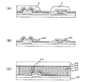
次に図6から図8により、本発明の3枚フォトマスクプロセスを説明する。端子部も含めて図1(E)のハーフトーン露光技術を必要とする第2のフォトマスク使用の工程から説明する。つまり、図1(E)から図6(A)とつながる。
(Embodiment 2)
Next, the three-photomask process of the present invention will be described with reference to FIGS. The process using a second photomask that requires the halftone exposure technique of FIG. That is, FIG. 1E is connected to FIG.
図6(A)において、ガラス基板100、ゲート電極101、絶縁膜102、配線311、島状I型アモルファスシリコン層123、一導電性を付与する不純物元素を有する半導体層、特に島状n+型アモルファスシリコン層124、金属膜105の上に、第2のフォトマスクを用いてフォトレジスト4を形成する。このフォトレジスト4は、ハーフトーン露光技術を用いる。つまり、異なる厚みを有するフォトレジストを形成する。ソース電極、ドレイン電極およびソース配線となる箇所は厚くし、チャネルとなる箇所は薄く形成する。
6A, a
図6(B)において、フォトレジスト4に覆われていないI型アモルファスシリコン層303、n+型アモルファスシリコン層304、金属膜105をエッチングする。
In FIG. 6B, the I-type
図6(C)において、アッシングによりフォトレジスト4を加工し、フォトレジスト5とする。 In FIG. 6C, the photoresist 4 is processed by ashing to form a photoresist 5.
図6(D)において、アッシングにより加工されたフォトレジスト5により、ソース電極309およびドレイン電極310を形成する。同様にフォトレジスト5によりチャネル領域306、ソース領域307およびドレイン領域308を形成する。その後、フォトレジスト5を除去する。ゲート絶縁膜を介してゲート電極と重なるI型アモルファスシリコン層123がチャネル領域306となる。
In FIG. 6D, the
図6(E)において、第3のフォトマスクを用いてフォトレジスト6を形成する。ここでもハーフトーン露光技術を使用する。フォトレジスト6に覆われていない絶縁膜102をエッチングし、コンタクトホール321を形成し、配線311を露出させる。配線311はアルミニウム、銅、チタン、モリブデン、クロム、タングステン、ネオジム等、他の導電膜との積層構造でも良い。この部分が端子部の透明導電膜との接続部になる。
In FIG. 6E, a
図7(A)において、アッシングによりフォトレジスト6を加工し、フォトレジスト7とする。
In FIG. 7A, the
図7(B)において、フォトレジスト7の上から透明導電膜312を成膜する。
In FIG. 7B, a transparent
図7(C)において、リフトオフ工程によりフォトレジスト7とその上に成膜されている透明導電膜312を除去することにより、画素電極313、配線320を作製する。その後、保護膜314を基板全面にCVD法により形成する。この保護膜とする絶縁膜は窒化珪素膜、酸化珪素膜、又はそれらの積層膜でも良い。窒化珪素膜はそのパッシベーション性能の高さから特に好ましい。
In FIG. 7C, the
図7(D)において、フォトレジストを保護膜314上に塗布し、裏面露光によりフォトレジストを選択的に露光し、所望のパターンのフォトレジスト8を形成する。ここで、透明な膜のみが、つまり前記する透明導電膜312および絶縁膜102のみが存在する部分においては、光が透過するため、フォトレジスト8が形成されない。裏面露光のため、チャネル領域において、ゲート電極101とソース電極309およびドレイン電極310は十分重なっている方が良い。
In FIG. 7D, a photoresist is applied on the
図8(A)において、前記裏面露光により形成したフォトレジスト8に熱処理を加え、リフロー処理する。すると、断面で見た場合、フォトレジスト8の端をリフロー処理前のフォトレジスト8の端の外側に僅かに拡張したように、フォトレジスト8はフォトレジスト9となる。また、リフロー処理により、フォトレジスト8の厚さも薄くなりフォトレジスト9となる。図には示さないが、上面で見た場合、フォトレジスト8の基板上の覆う範囲が僅かに広くなりフォトレジスト9となる。即ち、フォトレジストの端とソース電極およびドレイン電極の端の距離を広げる。リフロー処理は熱処理だけでなく薬剤処理によるものであっても良い。 In FIG. 8A, a heat treatment is applied to the photoresist 8 formed by the backside exposure, and a reflow process is performed. Then, when viewed in cross section, the photoresist 8 becomes the photoresist 9 as if the end of the photoresist 8 was slightly expanded outside the end of the photoresist 8 before the reflow process. Further, the thickness of the photoresist 8 is also reduced by the reflow process, so that the photoresist 9 is obtained. Although not shown in the drawing, when viewed from above, the area of the photoresist 8 covered on the substrate becomes slightly wider and becomes the photoresist 9. That is, the distance between the end of the photoresist and the ends of the source electrode and the drain electrode is increased. The reflow treatment may be performed not only by heat treatment but also by chemical treatment.
図8(B)において、リフロー処理によってフォトレジスト8の端がリフロー処理前の端の外側に僅かに拡張し、高さが低くなったフォトレジスト9を用いて、保護膜314をエッチングし、画素電極313を露出させる。この露出した領域は画素領域となる。このリフロー処理のためフォトレジスト8の端がリフロー処理前の端の外側に僅かに拡張したことにより、エッチング後の保護膜324が広がり、ソース電極およびドレイン電極の端の外側まで保護できるようになり、より確実に下層のTFTや電極を保護することができる。また、周辺部においてはコンタクトホール321を保護膜325により確実に保護することができる。
In FIG. 8B, the edge of the photoresist 8 is slightly expanded to the outside of the edge before the reflow process by the reflow process, and the
図8(C)は、図8(B)のTFT基板を用いて、LCDパネルを作製した場合の図である。TFTが作製されたガラス基板100に対向して対向基板319がある。対向基板319上にはカラーフィルタ318が形成されている。ガラス基板100と対向基板319の間には、液晶315およびスペーサ316があり、それをシール材317で封入している。
FIG. 8C illustrates a case where an LCD panel is manufactured using the TFT substrate of FIG. Opposing the
こうして、3回のフォトマスクを用いたフォトリソグラフィ工程により、逆スタガ型のnチャネル型TFTを完成させることができる。そして、これらを個々の画素に対応してマトリクス状に配置して画素部を構成することによりアクティブマトリクス型の電気光学装置を作製するための基板とすることができる。 Thus, an inverted staggered n-channel TFT can be completed by a photolithography process using a photomask three times. Then, by arranging these in a matrix corresponding to each pixel to form a pixel portion, a substrate for manufacturing an active matrix type electro-optical device can be obtained.
(実施の形態3)
次に図9を例にとり、画素部の周辺に設けられる周辺回路との接続端子部の構造について説明する。
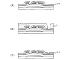
(Embodiment 3)
Next, taking FIG. 9 as an example, the structure of a connection terminal portion with a peripheral circuit provided around the pixel portion will be described.
図9(A)および図9(B)は、ソース配線が基板端まで引き回される場合の構造を示したものである。図9(A)は実施の形態1の場合、図9(B)は実施の形態2の場合を示したものである。なお、図1から図8と対応する箇所には同じ符号を用いている。図9(A)の場合、図3(B)のフォトレジスト3により、保護膜112をエッチングし、配線106を露出させて、透明導電膜114とコンタクトさせる。図9(B)の場合、図7(B)のフォトレジスト7により、金属膜105と透明導電膜312をコンタクトさせる。その後フォトレジスト9により、保護膜314をエッチングし、透明導電膜312を露出させる。これら透明導電膜114および312が接続端子となり、異方性導電膜などの導電性接着剤を介してFPC(フレキシブルプリントサーキット)などと接続する。
FIG. 9A and FIG. 9B show structures in the case where the source wiring is routed to the substrate end. FIG. 9A shows the case of the first embodiment, and FIG. 9B shows the case of the second embodiment. In addition, the same code | symbol is used for the location corresponding to FIGS. 1-8. In the case of FIG. 9A, the
図9(C)および図9(D)は、ゲート配線が基板端まで引き回される場合の構造を示したものである。図9(C)は実施の形態1の場合、図9(D)は実施の形態2の場合を示したものである。なお、図1から図8と対応する箇所には同じ符号を用いている。図9(C)の場合、図2(B)のフォトレジスト1により、ゲート絶縁膜102まで露出させ、図3(B)のフォトレジスト3により、ゲート絶縁膜102および保護膜112をエッチングし、ゲート配線と透明導電膜114とコンタクトさせる。図9(D)の場合、図6(E)のフォトレジスト6によりゲート電極301を露出させ、図7(B)のフォトレジスト7により、ゲート電極301と透明導電膜312とコンタクトさせる。その後フォトレジスト9により、保護膜314をエッチングし、透明導電膜312を露出させる。
FIG. 9C and FIG. 9D show a structure in the case where the gate wiring is routed to the substrate end. FIG. 9C shows the case of the first embodiment, and FIG. 9D shows the case of the second embodiment. In addition, the same code | symbol is used for the location corresponding to FIGS. 1-8. In the case of FIG. 9C, the
以上のように、従来の5枚のフォトマスクプロセスによる工程数に対して、4枚又は3枚のフォトマスクプロセスとしてマスク数を削減し、さらに工程数を削減した半導体装置を製造することができる。 As described above, the number of masks can be reduced as four or three photomask processes with respect to the number of steps by the conventional five photomask processes, and a semiconductor device with a further reduced number of steps can be manufactured. .
図11に本発明の半導体装置および電子機器の例として、テレビ、ノート型パーソナルコンピュータ、携帯情報端末(モバイルコンピュータ、携帯電話、携帯型ゲーム機又は電子書籍等)を示した。 FIG. 11 illustrates a television, a notebook personal computer, and a portable information terminal (mobile computer, cellular phone, portable game machine, electronic book, or the like) as examples of the semiconductor device and the electronic device of the present invention.
図11(A)は表示装置であり、筐体1001、表示部1002、スピーカ1003、ビデオ入力端子1004、支持台1005などを含む。この表示装置は、上述した実施の形態で示した作製方法により形成したTFTをその表示部1002および駆動回路に用いることにより作製される。なお、表示装置には液晶表示装置、発光装置などがあり、具体的にはコンピュータ用、テレビ受信用、広告表示用などの全ての情報表示用表示装置が含まれる。本発明により、安価な、信頼性の高い表示装置を実現することができる。
FIG. 11A illustrates a display device, which includes a
図11(B)で示す携帯電話機は、操作スイッチ類2001、表示部2002などを含む。本発明により、安価な、信頼性の高い携帯電話機を実現することができる。
A cellular phone shown in FIG. 11B includes operation switches 2001, a
図11(C)はノート型パーソナルコンピュータであり、本体3001、表示部3002等を含む。本発明により、安価な、信頼性の高いノート型パーソナルコンピュータを実現することができる。
FIG. 11C illustrates a laptop personal computer, which includes a
1 フォトレジスト
2 フォトレジスト
3 フォトレジスト
4 フォトレジスト
5 フォトレジスト
6 フォトレジスト
7 フォトレジスト
8 フォトレジスト
9 フォトレジスト
100 ガラス基板
101 ゲート電極、ゲート配線
102 絶縁膜、ゲート絶縁膜
103 I型アモルファスシリコン層
104 n+型アモルファスシリコン層
105 金属膜
106 配線
107 チャネル領域
108 ソース領域
109 ドレイン領域
110 ソース電極
111 ドレイン電極
112 保護膜
113 画素電極
114 透明導電膜
201 微結晶半導体膜
202 バッファ層
300 ガラス基板
301 ゲート電極
302 絶縁膜
303 I型アモルファスシリコン層
304 n+型アモルファスシリコン層
305 金属膜
306 チャネル領域
307 ソース領域
308 ドレイン領域
309 ソース電極
310 ドレイン電極
311 配線
312 透明導電膜
313 画素電極
314 保護膜
315 液晶
316 スペーサ
317 シール材
318 カラーフィルタ
319 対向基板
500 ガラス基板
501 ゲート電極
502 ゲート絶縁膜
503 I型アモルファスシリコン層
504 n+型アモルファスシリコン層
505 チャネル領域
506 ソース領域
507 ドレイン領域
508 ソース電極
509 ドレイン電極
510 保護膜
511 画素電極
DESCRIPTION OF SYMBOLS 1 Photoresist 2 Photoresist 3 Photoresist 4 Photoresist 5
Claims (5)
第一のフォトレジストを用いて前記金属膜をエッチングしゲート電極を形成し、
前記ゲート電極上にゲート絶縁膜を形成し、
前記ゲート絶縁膜上にI型半導体層を形成し、
前記I型半導体層上に一導電性を付与する不純物元素を含む半導体層を形成し、
第一の裏面露光を行って第二のフォトレジストを形成し、
前記第二のフォトレジストを用いて前記I型半導体層および前記一導電性を付与する不純物元素を含む半導体層をエッチングして島状に形成し、
前記基板上に第二の金属膜を形成し、
第一の多階調マスクを用いて第三のフォトレジストを形成し、
前記第三のフォトレジストを用いて前記第二の金属膜、前記一導電性を付与する不純物元素を含む半導体層および前記I型半導体層をエッチングし、
前記第三のフォトレジストをアッシングし、
アッシングされた前記第三のフォトレジストを用いて前記第二の金属膜をエッチングし、ソース電極およびドレイン電極を形成し、
アッシングされた前記第三のフォトレジストを用いて前記一導電性を付与する不純物元素を含む半導体層および前記I型半導体層をエッチングし、チャネル領域、ソース領域およびドレイン領域を形成し、
第二の多階調マスクを用いて第四のフォトレジストを形成し、
前記第四のフォトレジストを用いて前記第四のフォトレジストで覆われていない前記ゲート絶縁膜をエッチングしてコンタクトホールを形成し、
前記第四のフォトレジストをアッシングし、
前記基板上に導電膜を形成し、
前記第四のフォトレジストを除去することにより画素電極を形成し、
前記基板上に保護膜を形成し、
第二の裏面露光を行い前記保護膜上に第五のフォトレジストを形成し、
前記第五のフォトレジストをリフロー処理し、
リフロー処理された前記第五のフォトレジストを用いて前記保護膜をエッチングする半導体装置の作製方法。 Forming a first metal film on the substrate;
Etching the metal film using a first photoresist to form a gate electrode,
Forming a gate insulating film on the gate electrode;
Forming an I-type semiconductor layer on the gate insulating film;
Forming a semiconductor layer containing an impurity element imparting one conductivity on the I-type semiconductor layer;
Perform a first backside exposure to form a second photoresist,
Etching the I-type semiconductor layer and the semiconductor layer containing the impurity element imparting one conductivity with the second photoresist to form an island shape;
Forming a second metal film on the substrate;
Forming a third photoresist using the first multi-tone mask;
Etching the second metal film, the semiconductor layer containing the impurity element imparting one conductivity and the I-type semiconductor layer using the third photoresist,
Ashing the third photoresist,
Etching the second metal film using the ashed third photoresist, forming a source electrode and a drain electrode,
Etching the semiconductor layer containing the impurity element imparting the one conductivity and the I-type semiconductor layer using the ashed third photoresist to form a channel region, a source region, and a drain region,
Forming a fourth photoresist using a second multi-tone mask;
Etching the gate insulating film not covered with the fourth photoresist using the fourth photoresist to form a contact hole;
Ashing the fourth photoresist,
Forming a conductive film on the substrate;
Forming a pixel electrode by removing the fourth photoresist;
Forming a protective film on the substrate;
Perform a second backside exposure to form a fifth photoresist on the protective film,
Reflow the fifth photoresist;
A method for manufacturing a semiconductor device, wherein the protective film is etched using the fifth photoresist subjected to reflow processing.
Priority Applications (1)
| Application Number | Priority Date | Filing Date | Title |
|---|---|---|---|
| JP2008269324A JP5380037B2 (en) | 2007-10-23 | 2008-10-20 | Method for manufacturing semiconductor device |
Applications Claiming Priority (3)
| Application Number | Priority Date | Filing Date | Title |
|---|---|---|---|
| JP2007275781 | 2007-10-23 | ||
| JP2007275781 | 2007-10-23 | ||
| JP2008269324A JP5380037B2 (en) | 2007-10-23 | 2008-10-20 | Method for manufacturing semiconductor device |
Publications (3)
| Publication Number | Publication Date |
|---|---|
| JP2009124123A JP2009124123A (en) | 2009-06-04 |
| JP2009124123A5 JP2009124123A5 (en) | 2011-11-17 |
| JP5380037B2 true JP5380037B2 (en) | 2014-01-08 |
Family
ID=40722087
Family Applications (1)
| Application Number | Title | Priority Date | Filing Date |
|---|---|---|---|
| JP2008269324A Expired - Fee Related JP5380037B2 (en) | 2007-10-23 | 2008-10-20 | Method for manufacturing semiconductor device |
Country Status (2)
| Country | Link |
|---|---|
| US (2) | US20090148970A1 (en) |
| JP (1) | JP5380037B2 (en) |
Families Citing this family (23)
| Publication number | Priority date | Publication date | Assignee | Title |
|---|---|---|---|---|
| JP5357493B2 (en) * | 2007-10-23 | 2013-12-04 | 株式会社半導体エネルギー研究所 | Method for manufacturing semiconductor device |
| KR101448903B1 (en) | 2007-10-23 | 2014-10-13 | 가부시키가이샤 한도오따이 에네루기 켄큐쇼 | Semiconductor device and method for manufacturing semiconductor device |
| EP2232561A4 (en) * | 2007-12-03 | 2015-05-06 | Semiconductor Energy Lab | Manufacturing method of thin film transistor and manufacturing method of display device |
| KR101446249B1 (en) * | 2007-12-03 | 2014-10-01 | 가부시키가이샤 한도오따이 에네루기 켄큐쇼 | Method for manufacturing semiconductor device |
| US7910929B2 (en) * | 2007-12-18 | 2011-03-22 | Semiconductor Energy Laboratory Co., Ltd. | Semiconductor device |
| US8101442B2 (en) * | 2008-03-05 | 2012-01-24 | Semiconductor Energy Laboratory Co., Ltd. | Method for manufacturing EL display device |
| KR101237096B1 (en) * | 2008-08-21 | 2013-02-25 | 엘지디스플레이 주식회사 | Method for manufacturing thin film transistor array substrate |
| JP5361651B2 (en) | 2008-10-22 | 2013-12-04 | 株式会社半導体エネルギー研究所 | Method for manufacturing semiconductor device |
| KR101667909B1 (en) | 2008-10-24 | 2016-10-28 | 가부시키가이샤 한도오따이 에네루기 켄큐쇼 | Method for manufacturing semiconductor device |
| WO2010047288A1 (en) * | 2008-10-24 | 2010-04-29 | Semiconductor Energy Laboratory Co., Ltd. | Method for manufacturing semiconductordevice |
| EP2180518B1 (en) | 2008-10-24 | 2018-04-25 | Semiconductor Energy Laboratory Co, Ltd. | Method for manufacturing semiconductor device |
| US8741702B2 (en) | 2008-10-24 | 2014-06-03 | Semiconductor Energy Laboratory Co., Ltd. | Method for manufacturing semiconductor device |
| JP2010108957A (en) * | 2008-10-28 | 2010-05-13 | Hitachi Displays Ltd | Display device and method of manufacturing the same |
| JP5503995B2 (en) * | 2009-02-13 | 2014-05-28 | 株式会社半導体エネルギー研究所 | Method for manufacturing semiconductor device |
| KR101782176B1 (en) | 2009-07-18 | 2017-09-26 | 가부시키가이샤 한도오따이 에네루기 켄큐쇼 | Semiconductor device and method for manufacturing the same |
| JP5642447B2 (en) | 2009-08-07 | 2014-12-17 | 株式会社半導体エネルギー研究所 | Semiconductor device |
| TWI746064B (en) | 2009-08-07 | 2021-11-11 | 日商半導體能源研究所股份有限公司 | Semiconductor device and method for manufacturing the same |
| KR101940962B1 (en) | 2009-10-09 | 2019-01-21 | 가부시키가이샤 한도오따이 에네루기 켄큐쇼 | Semiconductor device |
| CN104465318B (en) * | 2009-11-06 | 2018-04-24 | 株式会社半导体能源研究所 | The method for manufacturing semiconductor devices |
| CN102148195B (en) | 2010-04-26 | 2013-05-01 | 北京京东方光电科技有限公司 | TFT-LCD (thin film transistor-liquid crystal display) array substrate and manufacturing method thereof |
| KR101748842B1 (en) * | 2010-08-24 | 2017-06-20 | 삼성디스플레이 주식회사 | An organic light emitting display device and the manufacturing method thereof |
| CN104377207A (en) * | 2014-08-29 | 2015-02-25 | 深超光电(深圳)有限公司 | Display panel and method for manufacturing display panel |
| CN105428243B (en) * | 2016-01-11 | 2017-10-24 | 京东方科技集团股份有限公司 | A kind of thin film transistor (TFT) and preparation method, array base palte and display device |
Family Cites Families (40)
| Publication number | Priority date | Publication date | Assignee | Title |
|---|---|---|---|---|
| JPS56122123A (en) * | 1980-03-03 | 1981-09-25 | Shunpei Yamazaki | Semiamorphous semiconductor |
| JPH0311744A (en) | 1989-06-09 | 1991-01-21 | Citizen Watch Co Ltd | Manufacture of thin film transistor |
| JP2814161B2 (en) * | 1992-04-28 | 1998-10-22 | 株式会社半導体エネルギー研究所 | Active matrix display device and driving method thereof |
| JP3173926B2 (en) * | 1993-08-12 | 2001-06-04 | 株式会社半導体エネルギー研究所 | Method of manufacturing thin-film insulated gate semiconductor device and semiconductor device thereof |
| EP1338914A3 (en) * | 1995-11-21 | 2003-11-19 | Samsung Electronics Co., Ltd. | Method for manufacturing liquid crystal display |
| US6493048B1 (en) | 1998-10-21 | 2002-12-10 | Samsung Electronics Co., Ltd. | Thin film transistor array panel for a liquid crystal display and a method for manufacturing the same |
| TW415109B (en) * | 1999-04-01 | 2000-12-11 | Hannstar Display Corp | Structure and fabrication of thin-film transistor (TFT) array |
| KR100325079B1 (en) * | 1999-12-22 | 2002-03-02 | 주식회사 현대 디스플레이 테크놀로지 | Method of manufacturing lcd having high aperture ratio and high transmittance |
| JP5408829B2 (en) * | 1999-12-28 | 2014-02-05 | ゲットナー・ファンデーション・エルエルシー | Method for manufacturing active matrix substrate |
| US7023021B2 (en) * | 2000-02-22 | 2006-04-04 | Semiconductor Energy Laboratory Co., Ltd. | Semiconductor device and method of manufacturing the same |
| US7223643B2 (en) * | 2000-08-11 | 2007-05-29 | Semiconductor Energy Laboratory Co., Ltd. | Method of manufacturing a semiconductor device |
| JP4570278B2 (en) * | 2000-08-28 | 2010-10-27 | シャープ株式会社 | Active matrix substrate |
| TW488080B (en) * | 2001-06-08 | 2002-05-21 | Au Optronics Corp | Method for producing thin film transistor |
| CN1267780C (en) * | 2002-11-11 | 2006-08-02 | Lg.飞利浦Lcd有限公司 | Array substrate for LCD device and its mfg. method |
| KR100971950B1 (en) * | 2003-06-30 | 2010-07-23 | 엘지디스플레이 주식회사 | Liquid Crystal Display and method for fabricating of the same |
| KR101112538B1 (en) * | 2004-07-27 | 2012-03-13 | 삼성전자주식회사 | THIN film transistor array panel and manufacturing Method thereof |
| KR101085136B1 (en) * | 2004-12-04 | 2011-11-18 | 엘지디스플레이 주식회사 | Thin film transistor substrate of horizontal electric field and fabricating method thereof |
| TWI262470B (en) * | 2004-12-24 | 2006-09-21 | Quanta Display Inc | Method of fabricating a pixel structure of a thin film transistor liquid crystal display |
| KR101107682B1 (en) * | 2004-12-31 | 2012-01-25 | 엘지디스플레이 주식회사 | Thin Film Transistor Substrate for Display Device And Method For Fabricating The Same |
| US7608490B2 (en) * | 2005-06-02 | 2009-10-27 | Semiconductor Energy Laboratory Co., Ltd. | Semiconductor device and manufacturing method thereof |
| US7588970B2 (en) | 2005-06-10 | 2009-09-15 | Semiconductor Energy Laboratory Co., Ltd. | Semiconductor device and manufacturing method thereof |
| KR101201017B1 (en) * | 2005-06-27 | 2012-11-13 | 엘지디스플레이 주식회사 | Liquid crystal display and fabricating method thereof |
| KR101225440B1 (en) * | 2005-06-30 | 2013-01-25 | 엘지디스플레이 주식회사 | Liquid crystal display and fabricating method thereof |
| US7807516B2 (en) * | 2005-06-30 | 2010-10-05 | Semiconductor Energy Laboratory Co., Ltd. | Semiconductor device and manufacturing method of the same |
| US7867791B2 (en) * | 2005-07-29 | 2011-01-11 | Semiconductor Energy Laboratory Co., Ltd. | Manufacturing method of semiconductor device using multiple mask layers formed through use of an exposure mask that transmits light at a plurality of intensities |
| US7914971B2 (en) * | 2005-08-12 | 2011-03-29 | Semiconductor Energy Laboratory Co., Ltd. | Light exposure mask and method for manufacturing semiconductor device using the same |
| US8149346B2 (en) * | 2005-10-14 | 2012-04-03 | Semiconductor Energy Laboratory Co., Ltd. | Display device and manufacturing method thereof |
| JP5105811B2 (en) | 2005-10-14 | 2012-12-26 | 株式会社半導体エネルギー研究所 | Display device |
| TWI460851B (en) * | 2005-10-17 | 2014-11-11 | Semiconductor Energy Lab | Semiconductor device and manufacturing method thereof |
| EP3229066A1 (en) * | 2005-12-05 | 2017-10-11 | Semiconductor Energy Laboratory Co., Ltd. | Transflective liquid crystal display with a horizontal electric field configuration |
| EP1958019B1 (en) * | 2005-12-05 | 2017-04-12 | Semiconductor Energy Laboratory Co., Ltd. | Liquid crystal display device |
| TWI400758B (en) * | 2005-12-28 | 2013-07-01 | Semiconductor Energy Lab | Manufacturing method of semiconductor device |
| US7821613B2 (en) * | 2005-12-28 | 2010-10-26 | Semiconductor Energy Laboratory Co., Ltd. | Display device and manufacturing method thereof |
| TWI297953B (en) * | 2006-02-22 | 2008-06-11 | Au Optronics Corp | Method for manufacturing a bottom substrate of a liquid crystal display device |
| TWI322288B (en) * | 2006-03-07 | 2010-03-21 | Au Optronics Corp | Manufacture method of pixel array substrate |
| KR101201972B1 (en) * | 2006-06-30 | 2012-11-15 | 삼성디스플레이 주식회사 | Thin film transistor array substrate and method for fabricating the same |
| TWI328880B (en) * | 2007-01-31 | 2010-08-11 | Au Optronics Corp | Method for fabricating a pixel structure of a liquid crystal display device |
| US8059236B2 (en) * | 2007-02-15 | 2011-11-15 | Au Optronics Corporation | Method for producing reflective layers in LCD display |
| KR101448903B1 (en) * | 2007-10-23 | 2014-10-13 | 가부시키가이샤 한도오따이 에네루기 켄큐쇼 | Semiconductor device and method for manufacturing semiconductor device |
| US7824939B2 (en) * | 2007-10-23 | 2010-11-02 | Semiconductor Energy Laboratory Co., Ltd. | Method for manufacturing display device comprising separated and electrically connected source wiring layers |
-
2008
- 2008-10-20 JP JP2008269324A patent/JP5380037B2/en not_active Expired - Fee Related
- 2008-10-21 US US12/255,312 patent/US20090148970A1/en not_active Abandoned
-
2014
- 2014-05-20 US US14/282,593 patent/US9564517B2/en active Active
Also Published As
| Publication number | Publication date |
|---|---|
| US9564517B2 (en) | 2017-02-07 |
| JP2009124123A (en) | 2009-06-04 |
| US20090148970A1 (en) | 2009-06-11 |
| US20140256095A1 (en) | 2014-09-11 |
Similar Documents
| Publication | Publication Date | Title |
|---|---|---|
| JP5380037B2 (en) | Method for manufacturing semiconductor device | |
| JP5600762B2 (en) | Semiconductor device | |
| US7420209B2 (en) | Semiconductor device | |
| JP4954366B2 (en) | Method for manufacturing semiconductor device | |
| JP6646329B2 (en) | Method for manufacturing low-temperature polysilicon array substrate | |
| JP5427390B2 (en) | Method for manufacturing semiconductor device | |
| WO2016061940A1 (en) | Thin film transistor array substrate and manufacturing method therefor, and display device | |
| JP2008181138A (en) | Display device | |
| US20210183912A1 (en) | Manufacturing method of tft array substrate | |
| US20080157086A1 (en) | Method for manufacturing thin film transistor | |
| WO2020140357A1 (en) | Thin film transistor, method of fabricating thin film transistor, and display apparatus having thin film transistor | |
| US20160181278A1 (en) | Array substrate, method for manufacturing the same, and display device | |
| JP4267242B2 (en) | Semiconductor device and manufacturing method thereof | |
| CN114089571A (en) | Array substrate, manufacturing method and display panel | |
| US8143624B2 (en) | Display device and method of manufacturing the same | |
| WO2011161875A1 (en) | Substrate for display device and process for production thereof, and display device | |
| JP2008177457A (en) | Method of manufacturing semiconductor device, method of manufacturing electro-optic device, and half-tone mask | |
| CN107735853B (en) | Thin film transistor manufacturing method and array substrate | |
| US20100155730A1 (en) | Thin film transistor display panel and manufacturing method thereof | |
| US10763283B2 (en) | Array substrate, manufacturing method thereof, display panel and manufacturing method thereof | |
| JP2005064344A (en) | Thin film semiconductor device, method for manufacturing the same, electro-optical device, and electronic apparatus | |
| US20160149043A1 (en) | Thin film transistor substrate and method of manufacturing the same | |
| JP4485481B2 (en) | Method for manufacturing semiconductor device | |
| JP2008083731A (en) | Semiconductor device | |
| CN113641048A (en) | Display device |
Legal Events
| Date | Code | Title | Description |
|---|---|---|---|
| A521 | Request for written amendment filed |
Free format text: JAPANESE INTERMEDIATE CODE: A523 Effective date: 20111004 |
|
| A621 | Written request for application examination |
Free format text: JAPANESE INTERMEDIATE CODE: A621 Effective date: 20111004 |
|
| A131 | Notification of reasons for refusal |
Free format text: JAPANESE INTERMEDIATE CODE: A131 Effective date: 20130730 |
|
| A977 | Report on retrieval |
Free format text: JAPANESE INTERMEDIATE CODE: A971007 Effective date: 20130731 |
|
| A521 | Request for written amendment filed |
Free format text: JAPANESE INTERMEDIATE CODE: A523 Effective date: 20130904 |
|
| TRDD | Decision of grant or rejection written | ||
| A01 | Written decision to grant a patent or to grant a registration (utility model) |
Free format text: JAPANESE INTERMEDIATE CODE: A01 Effective date: 20130924 |
|
| A61 | First payment of annual fees (during grant procedure) |
Free format text: JAPANESE INTERMEDIATE CODE: A61 Effective date: 20130930 |
|
| R150 | Certificate of patent or registration of utility model |
Ref document number: 5380037 Country of ref document: JP Free format text: JAPANESE INTERMEDIATE CODE: R150 Free format text: JAPANESE INTERMEDIATE CODE: R150 |
|
| R250 | Receipt of annual fees |
Free format text: JAPANESE INTERMEDIATE CODE: R250 |
|
| R250 | Receipt of annual fees |
Free format text: JAPANESE INTERMEDIATE CODE: R250 |
|
| R250 | Receipt of annual fees |
Free format text: JAPANESE INTERMEDIATE CODE: R250 |
|
| R250 | Receipt of annual fees |
Free format text: JAPANESE INTERMEDIATE CODE: R250 |
|
| R250 | Receipt of annual fees |
Free format text: JAPANESE INTERMEDIATE CODE: R250 |
|
| R250 | Receipt of annual fees |
Free format text: JAPANESE INTERMEDIATE CODE: R250 |
|
| LAPS | Cancellation because of no payment of annual fees |