JP5376930B2 - Method for manufacturing liquid discharge head - Google Patents
Method for manufacturing liquid discharge head Download PDFInfo
- Publication number
- JP5376930B2 JP5376930B2 JP2008323789A JP2008323789A JP5376930B2 JP 5376930 B2 JP5376930 B2 JP 5376930B2 JP 2008323789 A JP2008323789 A JP 2008323789A JP 2008323789 A JP2008323789 A JP 2008323789A JP 5376930 B2 JP5376930 B2 JP 5376930B2
- Authority
- JP
- Japan
- Prior art keywords
- mold
- active energy
- resin layer
- energy ray
- region
- Prior art date
- Legal status (The legal status is an assumption and is not a legal conclusion. Google has not performed a legal analysis and makes no representation as to the accuracy of the status listed.)
- Expired - Fee Related
Links
Images


Classifications
-
- B—PERFORMING OPERATIONS; TRANSPORTING
- B29—WORKING OF PLASTICS; WORKING OF SUBSTANCES IN A PLASTIC STATE IN GENERAL
- B29C—SHAPING OR JOINING OF PLASTICS; SHAPING OF MATERIAL IN A PLASTIC STATE, NOT OTHERWISE PROVIDED FOR; AFTER-TREATMENT OF THE SHAPED PRODUCTS, e.g. REPAIRING
- B29C43/00—Compression moulding, i.e. applying external pressure to flow the moulding material; Apparatus therefor
- B29C43/02—Compression moulding, i.e. applying external pressure to flow the moulding material; Apparatus therefor of articles of definite length, i.e. discrete articles
- B29C43/14—Compression moulding, i.e. applying external pressure to flow the moulding material; Apparatus therefor of articles of definite length, i.e. discrete articles in several steps
-
- B—PERFORMING OPERATIONS; TRANSPORTING
- B29—WORKING OF PLASTICS; WORKING OF SUBSTANCES IN A PLASTIC STATE IN GENERAL
- B29C—SHAPING OR JOINING OF PLASTICS; SHAPING OF MATERIAL IN A PLASTIC STATE, NOT OTHERWISE PROVIDED FOR; AFTER-TREATMENT OF THE SHAPED PRODUCTS, e.g. REPAIRING
- B29C43/00—Compression moulding, i.e. applying external pressure to flow the moulding material; Apparatus therefor
- B29C43/02—Compression moulding, i.e. applying external pressure to flow the moulding material; Apparatus therefor of articles of definite length, i.e. discrete articles
-
- B—PERFORMING OPERATIONS; TRANSPORTING
- B29—WORKING OF PLASTICS; WORKING OF SUBSTANCES IN A PLASTIC STATE IN GENERAL
- B29C—SHAPING OR JOINING OF PLASTICS; SHAPING OF MATERIAL IN A PLASTIC STATE, NOT OTHERWISE PROVIDED FOR; AFTER-TREATMENT OF THE SHAPED PRODUCTS, e.g. REPAIRING
- B29C35/00—Heating, cooling or curing, e.g. crosslinking or vulcanising; Apparatus therefor
- B29C35/02—Heating or curing, e.g. crosslinking or vulcanizing during moulding, e.g. in a mould
- B29C35/08—Heating or curing, e.g. crosslinking or vulcanizing during moulding, e.g. in a mould by wave energy or particle radiation
- B29C35/0888—Heating or curing, e.g. crosslinking or vulcanizing during moulding, e.g. in a mould by wave energy or particle radiation using transparant moulds
- B29C35/0894—Heating or curing, e.g. crosslinking or vulcanizing during moulding, e.g. in a mould by wave energy or particle radiation using transparant moulds provided with masks or diaphragms
-
- B—PERFORMING OPERATIONS; TRANSPORTING
- B29—WORKING OF PLASTICS; WORKING OF SUBSTANCES IN A PLASTIC STATE IN GENERAL
- B29C—SHAPING OR JOINING OF PLASTICS; SHAPING OF MATERIAL IN A PLASTIC STATE, NOT OTHERWISE PROVIDED FOR; AFTER-TREATMENT OF THE SHAPED PRODUCTS, e.g. REPAIRING
- B29C43/00—Compression moulding, i.e. applying external pressure to flow the moulding material; Apparatus therefor
- B29C43/003—Compression moulding, i.e. applying external pressure to flow the moulding material; Apparatus therefor characterised by the choice of material
-
- B—PERFORMING OPERATIONS; TRANSPORTING
- B29—WORKING OF PLASTICS; WORKING OF SUBSTANCES IN A PLASTIC STATE IN GENERAL
- B29C—SHAPING OR JOINING OF PLASTICS; SHAPING OF MATERIAL IN A PLASTIC STATE, NOT OTHERWISE PROVIDED FOR; AFTER-TREATMENT OF THE SHAPED PRODUCTS, e.g. REPAIRING
- B29C43/00—Compression moulding, i.e. applying external pressure to flow the moulding material; Apparatus therefor
- B29C43/02—Compression moulding, i.e. applying external pressure to flow the moulding material; Apparatus therefor of articles of definite length, i.e. discrete articles
- B29C43/021—Compression moulding, i.e. applying external pressure to flow the moulding material; Apparatus therefor of articles of definite length, i.e. discrete articles characterised by the shape of the surface
-
- B—PERFORMING OPERATIONS; TRANSPORTING
- B82—NANOTECHNOLOGY
- B82Y—SPECIFIC USES OR APPLICATIONS OF NANOSTRUCTURES; MEASUREMENT OR ANALYSIS OF NANOSTRUCTURES; MANUFACTURE OR TREATMENT OF NANOSTRUCTURES
- B82Y10/00—Nanotechnology for information processing, storage or transmission, e.g. quantum computing or single electron logic
-
- B—PERFORMING OPERATIONS; TRANSPORTING
- B82—NANOTECHNOLOGY
- B82Y—SPECIFIC USES OR APPLICATIONS OF NANOSTRUCTURES; MEASUREMENT OR ANALYSIS OF NANOSTRUCTURES; MANUFACTURE OR TREATMENT OF NANOSTRUCTURES
- B82Y40/00—Manufacture or treatment of nanostructures
-
- G—PHYSICS
- G03—PHOTOGRAPHY; CINEMATOGRAPHY; ANALOGOUS TECHNIQUES USING WAVES OTHER THAN OPTICAL WAVES; ELECTROGRAPHY; HOLOGRAPHY
- G03F—PHOTOMECHANICAL PRODUCTION OF TEXTURED OR PATTERNED SURFACES, e.g. FOR PRINTING, FOR PROCESSING OF SEMICONDUCTOR DEVICES; MATERIALS THEREFOR; ORIGINALS THEREFOR; APPARATUS SPECIALLY ADAPTED THEREFOR
- G03F7/00—Photomechanical, e.g. photolithographic, production of textured or patterned surfaces, e.g. printing surfaces; Materials therefor, e.g. comprising photoresists; Apparatus specially adapted therefor
- G03F7/0002—Lithographic processes using patterning methods other than those involving the exposure to radiation, e.g. by stamping
-
- B—PERFORMING OPERATIONS; TRANSPORTING
- B29—WORKING OF PLASTICS; WORKING OF SUBSTANCES IN A PLASTIC STATE IN GENERAL
- B29C—SHAPING OR JOINING OF PLASTICS; SHAPING OF MATERIAL IN A PLASTIC STATE, NOT OTHERWISE PROVIDED FOR; AFTER-TREATMENT OF THE SHAPED PRODUCTS, e.g. REPAIRING
- B29C43/00—Compression moulding, i.e. applying external pressure to flow the moulding material; Apparatus therefor
- B29C43/02—Compression moulding, i.e. applying external pressure to flow the moulding material; Apparatus therefor of articles of definite length, i.e. discrete articles
- B29C43/021—Compression moulding, i.e. applying external pressure to flow the moulding material; Apparatus therefor of articles of definite length, i.e. discrete articles characterised by the shape of the surface
- B29C2043/023—Compression moulding, i.e. applying external pressure to flow the moulding material; Apparatus therefor of articles of definite length, i.e. discrete articles characterised by the shape of the surface having a plurality of grooves
- B29C2043/025—Compression moulding, i.e. applying external pressure to flow the moulding material; Apparatus therefor of articles of definite length, i.e. discrete articles characterised by the shape of the surface having a plurality of grooves forming a microstructure, i.e. fine patterning
-
- B—PERFORMING OPERATIONS; TRANSPORTING
- B29—WORKING OF PLASTICS; WORKING OF SUBSTANCES IN A PLASTIC STATE IN GENERAL
- B29C—SHAPING OR JOINING OF PLASTICS; SHAPING OF MATERIAL IN A PLASTIC STATE, NOT OTHERWISE PROVIDED FOR; AFTER-TREATMENT OF THE SHAPED PRODUCTS, e.g. REPAIRING
- B29C43/00—Compression moulding, i.e. applying external pressure to flow the moulding material; Apparatus therefor
- B29C43/02—Compression moulding, i.e. applying external pressure to flow the moulding material; Apparatus therefor of articles of definite length, i.e. discrete articles
- B29C43/14—Compression moulding, i.e. applying external pressure to flow the moulding material; Apparatus therefor of articles of definite length, i.e. discrete articles in several steps
- B29C2043/141—Compression moulding, i.e. applying external pressure to flow the moulding material; Apparatus therefor of articles of definite length, i.e. discrete articles in several steps for making single layer articles
- B29C2043/144—Compression moulding, i.e. applying external pressure to flow the moulding material; Apparatus therefor of articles of definite length, i.e. discrete articles in several steps for making single layer articles using different moulds, i.e. the layer is compressed in consecutive steps by using different moulds for each portion of the article
-
- B—PERFORMING OPERATIONS; TRANSPORTING
- B29—WORKING OF PLASTICS; WORKING OF SUBSTANCES IN A PLASTIC STATE IN GENERAL
- B29C—SHAPING OR JOINING OF PLASTICS; SHAPING OF MATERIAL IN A PLASTIC STATE, NOT OTHERWISE PROVIDED FOR; AFTER-TREATMENT OF THE SHAPED PRODUCTS, e.g. REPAIRING
- B29C59/00—Surface shaping of articles, e.g. embossing; Apparatus therefor
- B29C59/02—Surface shaping of articles, e.g. embossing; Apparatus therefor by mechanical means, e.g. pressing
- B29C59/022—Surface shaping of articles, e.g. embossing; Apparatus therefor by mechanical means, e.g. pressing characterised by the disposition or the configuration, e.g. dimensions, of the embossments or the shaping tools therefor
- B29C2059/023—Microembossing
-
- B—PERFORMING OPERATIONS; TRANSPORTING
- B29—WORKING OF PLASTICS; WORKING OF SUBSTANCES IN A PLASTIC STATE IN GENERAL
- B29C—SHAPING OR JOINING OF PLASTICS; SHAPING OF MATERIAL IN A PLASTIC STATE, NOT OTHERWISE PROVIDED FOR; AFTER-TREATMENT OF THE SHAPED PRODUCTS, e.g. REPAIRING
- B29C43/00—Compression moulding, i.e. applying external pressure to flow the moulding material; Apparatus therefor
- B29C43/02—Compression moulding, i.e. applying external pressure to flow the moulding material; Apparatus therefor of articles of definite length, i.e. discrete articles
- B29C43/04—Compression moulding, i.e. applying external pressure to flow the moulding material; Apparatus therefor of articles of definite length, i.e. discrete articles using movable moulds
Abstract
Description
本発明は、モールドによる微細三次元構造の形成方法に関する。 The present invention relates to a method for forming a fine three-dimensional structure using a mold.
微細三次元構造の形成方法として、従来の機械加工やフォトリソグラフィの限界に制限されない分解能を持つナノインプリント法が注目されている。 As a method for forming a fine three-dimensional structure, a nanoimprint method having a resolution that is not limited by the limitations of conventional machining and photolithography has attracted attention.
ナノインプリント法は、例えば、まず表面に薄膜化したポリメチルメタクリレート(PMMA)等の熱可塑性樹脂が形成された基板と、微細な凹凸パターンが形成されたモールドを用意する。次に、前記基板をガラス転移点以上まで加熱することで軟化した熱可塑性樹脂にモールドをプレスする。そして、ガラス転移点以下になるまで冷却することにより固化した熱可塑性樹脂からモールドを離型する。このようにして、モールドの微細パターンの反転パターンを熱可塑性樹脂に形成する(特許文献1参照)。 In the nanoimprint method, for example, first, a substrate on which a thermoplastic resin such as polymethyl methacrylate (PMMA) having a thin film is formed and a mold on which a fine uneven pattern is formed are prepared. Next, the mold is pressed into a thermoplastic resin softened by heating the substrate to a glass transition point or higher. Then, the mold is released from the thermoplastic resin solidified by cooling until the glass transition point or lower. In this way, a reverse pattern of the fine pattern of the mold is formed on the thermoplastic resin (see Patent Document 1).
一方、表面に薄膜化した活性エネルギー線硬化性樹脂層が形成された基板を用いた場合は、例えば石英等の活性エネルギー線透過性材料から成り微細な凹凸パターンが形成されたモールドを用意する。次に、基板上の活性エネルギー線硬化性樹脂層にモールドをプレスし、前記基板を透して活性エネルギー線を照射することにより活性エネルギー線硬化性樹脂を硬化させモールドを離型する。このようにして、モールドの微細パターンの反転パターンを活性エネルギー線硬化性樹脂層に形成する(特許文献2参照)。 On the other hand, when a substrate having a thin active energy ray-curable resin layer formed on the surface is used, a mold made of an active energy ray-transmitting material such as quartz and having a fine uneven pattern is prepared. Next, the mold is pressed on the active energy ray curable resin layer on the substrate, and the active energy ray curable resin is cured by irradiating the substrate with the active energy ray to release the mold. In this way, a reverse pattern of the fine pattern of the mold is formed on the active energy ray curable resin layer (see Patent Document 2).
以上のように、ナノインプリント法では、所望のパターンが形成されたモールドを用意することが必要とされる。モールドの作製方法としては、露光、現像技術とエッチング技術を用いることによりシリコン、Niや石英のモールドを作製する方法等がある。 As described above, in the nanoimprint method, it is necessary to prepare a mold in which a desired pattern is formed. As a method for producing a mold, there is a method for producing a mold of silicon, Ni or quartz by using an exposure, development technique and etching technique.
しかし、複数の段を有する微細三次元構造のモールドを作製するためには、エッチングを繰り返し行う必要がある。そのため、凹凸パターンの深さや高さを一定にすることやエッヂの形状を保つことが困難であるばかりでなく、活性エネルギー線透過性材料である石英を用いる場合、マイクロトレンチが発生し精度のよいモールドを作製することが困難である。 However, in order to produce a mold having a fine three-dimensional structure having a plurality of steps, it is necessary to repeatedly perform etching. Therefore, not only is it difficult to keep the depth and height of the concavo-convex pattern constant and the shape of the edge, but when using quartz, which is an active energy ray transmissive material, micro-trench is generated and high accuracy It is difficult to produce a mold.
そこで、1段の凸部からなるモールドを複数個用いて、複数回のプレスを行うことで微細三次元構造を形成する方法が考えられる。しかし、上記特許文献1のような熱インプリント方式におけるプレス過程は高温で行う必要がある。そのため、あるパターンを形成した基板を再びガラス転移点以上まで加熱しプレスを行おうとすると、熱可塑性樹脂にプレスされていたパターンが軟化してしまうため形状が維持できなくなる。従って、熱インプリント方式において複数個のモールドを用いて、複数回のプレスを行い、微細三次元構造を精度良く形成することは困難である。
Therefore, a method of forming a fine three-dimensional structure by performing a plurality of presses using a plurality of molds made of one-step convex portions can be considered. However, the pressing process in the thermal imprint method as in
一方、加熱をせずにプレスを行う方法として、基板上の熱可塑性樹脂に多孔質構造を形成し、ガラス転移温度以下でインプリントを行う方法がある(特許文献3参照)。この方法では、プレス時に熱可塑性樹脂内の多孔質体積が減少することでプレス力を吸収し、パターン形成を行う。
既に述べたように、1段の凸部からなるモールドを複数個用いて、複数回のプレスを行うことで微細三次元構造を形成する際に加熱をしない方法として、基板上の熱可塑性樹脂に多孔質構造を形成し、ガラス転移温度以下でインプリントを行う方法は知られている。しかし、この方法を用いた場合、プレスを繰り返すごとに多孔質は減少していくのでプレス力は吸収されなくなり、プレスするパターンの周囲への影響が無視できず、熱可塑性樹脂にプレスされていたパターンが崩れていってしまうことが考えられる。 As already mentioned, as a method of not heating when forming a fine three-dimensional structure by performing multiple presses using a plurality of molds made of one-step convex portions, a thermoplastic resin on a substrate is used. A method for forming a porous structure and imprinting at a glass transition temperature or lower is known. However, when this method is used, the porosity decreases each time the press is repeated, so the pressing force is not absorbed, and the influence on the periphery of the pattern to be pressed cannot be ignored, and it is pressed to a thermoplastic resin. It is possible that the pattern is broken.
従って、多孔質構造を形成した熱可塑性樹脂を室温インプリント方式において、複数個のモールドを用いて、複数回のプレスを繰り返し行い、微細三次元構造を形成することは困難であった。 Therefore, it has been difficult to form a fine three-dimensional structure by repeatedly pressing a thermoplastic resin having a porous structure in a room temperature imprint method by using a plurality of molds and pressing a plurality of times.
本発明の液体吐出ヘッドの製造方法は、
基板の上に、活性エネルギー線硬化性樹脂からなる樹脂層を形成する工程と、
前記樹脂層の上から、活性エネルギー線透過性材料で作製され、表面に凸部が形成されており、その凸部に活性エネルギー線遮蔽膜が形成された第一のモールドをプレスして、前記樹脂層に前記第一のモールドの凸部に対応した凹部を形成する工程と、
前記第一のモールドを介して、前記樹脂層に活性エネルギー線を照射して、前記樹脂層に前記活性エネルギー線硬化性樹脂が硬化した領域と前記活性エネルギー線硬化性樹脂が未硬化の領域を形成する工程と、
前記第一のモールドを前記樹脂層から離型する工程と、
前記樹脂層の上から、表面に凸部が形成された第二のモールドをプレスして、前記活性エネルギー線硬化性樹脂が未硬化の領域に前記第二のモールドの凸部に対応した凹部を形成し、三次元構造を有する樹脂層を形成する工程と、
前記三次元構造を有する樹脂層と、液体吐出エネルギー発生素子を有する基板とを貼り合わせる工程と、を有することを特徴とする。
The manufacturing method of the liquid discharge head of the present invention includes
Forming a resin layer made of an active energy ray-curable resin on the substrate;
From the top of the resin layer, made of an active energy ray transmissive material, a convex portion is formed on the surface, and a first mold having an active energy ray shielding film formed on the convex portion is pressed, Forming a concave portion corresponding to the convex portion of the first mold in the resin layer;
The resin layer is irradiated with active energy rays through the first mold, and a region where the active energy ray-curable resin is cured and a region where the active energy ray-curable resin is uncured are formed on the resin layer. Forming, and
Releasing the first mold from the resin layer;
From above the resin layer, a second mold having a convex portion formed on the surface is pressed, and a concave portion corresponding to the convex portion of the second mold is formed in a region where the active energy ray-curable resin is uncured. Forming and forming a resin layer having a three-dimensional structure ;
And a step of bonding the resin layer having the three-dimensional structure and a substrate having a liquid discharge energy generating element .
本発明の液体吐出ヘッドの製造方法によれば、硬化した樹脂が未硬化な樹脂を囲んでいるため、プレスするパターン周囲への影響が抑えられることにより、複数個のモールドを用いて複数回のプレスにより三次元構造を形成することができる。 According to the method for manufacturing a liquid discharge head of the present invention, since the cured resin surrounds the uncured resin, the influence on the periphery of the pattern to be pressed is suppressed. it is possible to form a three-dimensional structure Ri by the press.
以下、添付図面に基づいて、本発明の実施形態について説明する。 Hereinafter, embodiments of the present invention will be described with reference to the accompanying drawings.
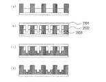
図1に、本発明の実施形態の一例であるインプリント用モールドによる微細三次元構造の形成方法の概略図を示す。 FIG. 1 shows a schematic diagram of a method for forming a fine three-dimensional structure using an imprint mold as an example of an embodiment of the present invention.
まず、図1(a)に示すように、表面に凸部が形成されており、その凸部に活性エネルギー線遮蔽膜102が形成された第一のモールド101を準備する。第一のモールド101に形成された凸部は、1段でよい。第一のモールド101は、活性エネルギー線透過性材料からなっており、例えば石英で作製されている。また、活性エネルギー線遮蔽膜102は、活性エネルギー線の透過を遮る材質よりなっており、例えばクロム(Cr)で作製されている。
First, as shown in FIG. 1A, a
一方、図1(b)に示すように、活性エネルギー線硬化性樹脂からなる樹脂層103を塗布した基板104を準備する。活性エネルギー線硬化性樹脂は、離型時に活性エネルギー線遮蔽膜下の未硬化な樹脂がモールドとともに引き剥がされるのを防ぐために、室温で固体の樹脂を溶媒に溶かしたものが好ましく、例えばSU−8(商品名、化薬マイクロケム社製)で作製されている。また、基板104は、プレス時に変形しない強度と、モールドの凹凸構造以下の平滑性が得られるものであればよく、例えばシリコン(Si)で作製されている。
On the other hand, as shown in FIG.1 (b), the board |
次に、図1(c)に示すように、樹脂層103の上から、第一のモールド101を適切な力でプレスする。それにより、樹脂層103は変形し、第一のモールドの凸部に対応した凹部106と残部の凸部105とが形成される。このとき、プレス力を小さくするために、樹脂層103及び基板104を加熱してもよい。
Next, as shown in FIG. 1C, the
次に、図1(d)に示すように、第一のモールド101を樹脂層103にプレスした状態で、第一のモールド101を介して活性エネルギー線を照射する。第一のモールド101は活性エネルギー線を透過する材質よりなっているため、照射された活性エネルギー線は第一のモールド101を透過して樹脂層103に照射される。ただし、活性エネルギー線遮蔽膜102が活性エネルギー線を遮る材質よりなっているため、樹脂層103の凹部106には活性エネルギー線は照射されない。そのため、活性エネルギー線照射により、樹脂層103の凸部105は活性エネルギー線硬化性樹脂が硬化した硬化領域107となり、樹脂層103の凹部106は、活性エネルギー線硬化性樹脂が架橋していない未硬化領域108となる。すなわち、未硬化領域108が硬化領域107で囲まれた樹脂層109が形成される。
Next, as shown in FIG. 1D, active energy rays are irradiated through the
次に、図1(e)に示すように、第一のモールド101を樹脂層109から離型する。離型前に、樹脂層109を充分に冷却することが好ましい。また、使用する活性エネルギー線硬化性樹脂によっては、活性エネルギー線照射のみで硬化が不充分な場合もあるが、その場合は、第一のモールド101をプレスした状態、又は第一のモールド101を離型した直後に加熱して充分に硬化させてもよい。
Next, as shown in FIG. 1E, the
次に、図1(f)に示すように、樹脂層109の上から、第二のモールド111を適切な力でプレスする。第二のモールド111は、活性エネルギー線透過性材料からなっており、例えば石英で作製されている。また、第二のモールド111の表面には凸部が形成されており、その凸部には活性エネルギー線遮蔽膜110が形成されている。第二のモールド111に形成された凸部は、1段でよい。活性エネルギー線遮蔽膜110は、活性エネルギー線の透過を遮る材質よりなっており、例えばクロム(Cr)で作製されている。それにより、未硬化領域108は変形し、第二のモールドの凸部に対応した凹部113と残部の凸部112とが形成される。このとき、プレス力を小さくするために、樹脂層109及び基板104を加熱してもよい。
Next, as shown in FIG. 1F, the
なお、第一のモールド101により形成した凸部105は、活性エネルギー線の照射により硬化しているため、第二のモールド111でプレスしても形状が崩れることはない。また、未硬化領域108が硬化領域107により囲まれているため、モールドにより押しのけられた樹脂が、第二のモールド111と樹脂層109の間の空間114に盛り上がってくることが考えられる。しかし、未硬化領域108が図1の奥行き方向に、第二のモールド111に対して充分に大きい体積を有する場合には、第二のモールド111と樹脂層109の間の空間114における樹脂表面の変位は極めて小さい。
In addition, since the
第二のモールド111は、プレスする未硬化領域108より微細なパターンを含むモールドである。すなわち、第二のモールド111に形成された1つの凸部の断面積は、1つの未硬化領域108の面積よりも小さい。
The
次に、図1(g)に示すように、第二のモールド111を未硬化領域108にプレスした状態で、第二のモールド111を介して活性エネルギー線を照射する。第二のモールド111は活性エネルギー線を透過する材質よりなっているため、照射された活性エネルギー線は第二のモールド111を透過して樹脂層109に照射される。ただし、活性エネルギー線遮蔽膜110が活性エネルギー線を遮る材質よりなっているため、未硬化領域108の凹部113には活性エネルギー線は照射されない。そのため、活性エネルギー線照射により、未硬化領域108の凸部112は、活性エネルギー線硬化性樹脂が硬化した硬化領域115となり、未硬化領域108の凹部113は、活性エネルギー線硬化性樹脂が架橋していない未硬化領域116となる。すなわち、未硬化領域116が硬化領域115で囲まれた樹脂層117が形成される。
Next, as shown in FIG. 1G, active energy rays are irradiated through the
次に、図1(h)に示すように、第二のモールド111を樹脂層117から離型する。離型前に、樹脂層117を充分に冷却することが好ましい。また、使用する活性エネルギー線硬化性樹脂によっては、活性エネルギー線照射のみで硬化が不充分な場合もあるが、その場合は、第二のモールド111をプレスした状態、又は第二のモールド111を離型した直後に加熱し充分に硬化させてもよい。このようにして、1段の凸部からなるモールドを2個用いて、2段の微細三次元構造を形成することができる。
Next, as shown in FIG. 1 (h), the
本発明の実施形態としては、第nのモールド(nは3以上の整数)を用いて、さらに図1(c)〜(h)の工程を(n−2)回繰り返すことにより、所望の微細三次元構造を形成してもよい。第nのモールドに形成された凸部は、1段でよい。このようにして、1段の凸部からなるモールドを3個以上用いて、3段以上の構造微細三次元構造を形成することができる。 As an embodiment of the present invention, by using the nth mold (n is an integer of 3 or more), the steps of FIGS. 1C to 1H are further repeated (n−2) times to obtain a desired fineness. A three-dimensional structure may be formed. The convex part formed in the nth mold may be one step. In this way, it is possible to form a three-stage or more structured fine three-dimensional structure by using three or more molds made of one-step convex portions.
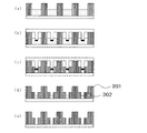
本発明の実施形態としては、図1(e)〜(h)の工程の代わりに、図2(a)〜(d)の工程とすることもできる。すなわち、最後のモールドとして活性エネルギー線遮蔽膜が形成されていないモールド201を用いて、活性エネルギー線を全面照射することで、硬化領域202で囲まれた未硬化領域203の樹脂を硬化させてもよい。
As an embodiment of the present invention, the steps shown in FIGS. 2A to 2D can be used instead of the steps shown in FIGS. That is, even if the resin in the
本発明の実施の形態としては、図1(e)〜(h)の工程の代わりに、図3(a)〜(e)の工程とすることもできる。すなわち、最後のモールドを離型した後、硬化領域301で囲まれた未硬化領域302の樹脂を現像により除去してもよい。また、図1(h)の状態で、活性エネルギー線を全面照射することで、硬化領域115で囲まれた未硬化領域116の樹脂を硬化させてもよい。
As an embodiment of the present invention, the steps shown in FIGS. 3A to 3E may be used instead of the steps shown in FIGS. That is, after the last mold is released, the resin in the
本発明の実施の形態として、液体吐出ヘッドの製造方法を示す。液体吐出ヘッドとは、熱エネルギーを液体に作用させて気泡を発生させることにより、液体を吐出する装置である。 As an embodiment of the present invention, a method for manufacturing a liquid discharge head will be described. A liquid discharge head is a device that discharges liquid by causing thermal energy to act on the liquid to generate bubbles.
液体吐出ヘッドの構成を図4に示す。この液体吐出ヘッドは、基板401と基板402とから構成されている。基板401は、液体を吐出するための吐出口と、その吐出口に一端部が連通され、気泡を発生させる領域を含む液体流路とを有している。基板402は、気泡を発生させるための液体吐出エネルギー発生素子と液体流路と連通するよう形成された液体供給口を有している。
The configuration of the liquid discharge head is shown in FIG. This liquid discharge head is composed of a
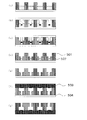
本発明の実施の形態により液体吐出ヘッドを製造する場合、図1(e)〜(h)の工程の代わりに、図5(a)〜(g)の工程とすることができる。すなわち、最後のモールドを離型した後、図5(e)に示すように、硬化領域501で囲まれた未硬化領域502の樹脂を現像により除去する。その後、樹脂層と、液体吐出エネルギー発生素子と液体流路とを有する基板503とを貼り合わせ、樹脂層を支持していた基板504を剥離する。こうすることで、液体吐出ヘッドを製造することができる。
When the liquid discharge head is manufactured according to the embodiment of the present invention, the steps shown in FIGS. 5A to 5G can be used instead of the steps shown in FIGS. That is, after the last mold is released, the resin in the
図6に、本発明の他の実施形態であるインプリント用モールドによる微細三次元構造の形成方法の概略図を示す。所望のパターンがインプリント面内で一様でなく、複数回のプレスを繰り返して高さの等しい段差を形成したい場合に、有効である。なお、前述の実施形態と同様の部分は説明を省略している。 FIG. 6 shows a schematic diagram of a method for forming a fine three-dimensional structure using an imprint mold according to another embodiment of the present invention. This is effective when the desired pattern is not uniform within the imprint surface and it is desired to form steps having the same height by repeating a plurality of presses. Note that the description of the same parts as those in the above embodiment is omitted.
まず、図6(a)に示すように、基板の上に形成された活性エネルギー線硬化性樹脂からなる樹脂層603の上から、活性エネルギー線遮蔽膜601付きの活性エネルギー線透過性材料からなる第一のモールド602を適切な力でプレスする。なお、活性エネルギー線遮蔽膜601は、図6(a)に示すように、第一のモールド602の凸部だけでなく、凹部の一部にも形成されている。
First, as shown in FIG. 6A, an active energy ray-transmitting material with an active energy
次に、図6(b)に示すように、第一のモールド602を樹脂層603にプレスした状態で、第一のモールド602を介して活性エネルギー線を照射する。ただし、樹脂層603の凸部が全て活性エネルギー線の照射を受けるわけではなく、第一のモールド602の凹部において活性エネルギー線遮蔽膜601が形成された領域に対応した部分は照射を受けず、未硬化領域のままである。これにより、未硬化領域605が硬化領域604で囲まれた樹脂層606が形成される。
Next, as shown in FIG. 6B, active energy rays are irradiated through the
次に、図6(c)に示すように、第一のモールド602を樹脂層606から離型する。
Next, as shown in FIG. 6C, the
次に、図6(d)に示すように、樹脂層606の上から、活性エネルギー線遮蔽膜607付きの活性エネルギー線透過性材料からなる第二のモールド608を適切な力でプレスする。第二のモールド608は、第一のモールド602とアスペクト比が異なるモールドである。なお、活性エネルギー線遮蔽膜606は、図6(d)に示すように、第二のモールド608の凸部だけでなく、凹部の一部にも形成されている。
Next, as shown in FIG. 6D, a
次に、図6(e)に示すように、第二のモールド608を未硬化領域605にプレスした状態で、第二のモールド608を介して活性エネルギー線を照射する。ただし、樹脂層603の凸部が全て活性エネルギー線の照射を受けるわけではなく、第二のモールド60608の凹部において活性エネルギー線遮蔽膜606が形成された領域に対応した部分は照射を受けず、未硬化領域のままである。これにより、硬化領域609で囲まれた表面高さの低い未硬化領域である凹部610と、硬化領域609で囲まれた表面高さの高い未硬化領域である凹部611とが形成された樹脂層となる。
Next, as shown in FIG. 6E, active energy rays are irradiated through the
次に、図6(f)に示すように、第二のモールド608を樹脂層から離型する。
Next, as shown in FIG. 6F, the
ここで、未硬化領域である凹部610及び611の高さを調整しておく。すなわち、モールドにより押しのけられる樹脂の体積と、モールドと樹脂の間の空間で盛り上がる樹脂の体積が等しいことから、以下に続く第三、第四のモールドでプレスした際に盛り上がる樹脂表面の高さが等しくなるように調整する。
Here, the heights of the
次に、図6(g)に示すように、樹脂層の上から、活性エネルギー線遮蔽膜612付の活性エネルギー線透過性材料からなる第三のモールド613を適切な力でプレスする。なお、活性エネルギー線遮蔽膜612は、図6(g)に示すように、第三のモールド613の凹部の一部に形成されており、凸部には形成されていない。こうすることで、凹部610の樹脂はプレスされるともに押しのけられ、所望の形状となる。
Next, as shown in FIG. 6G, a
次に、図6(h)に示すように、第三のモールド613を凹部610にプレスした状態で、第三のモールド613を介して活性エネルギー線を照射する。これにより、凹部610の樹脂が硬化して、所望の構造となる。
Next, as shown in FIG. 6H, active energy rays are irradiated through the
次に、図6(i)に示すように、第三のモールド613を樹脂層から離型する。
Next, as shown in FIG. 6I, the
次に、図6(j)に示すように、樹脂層の上から、活性エネルギー線透過性材料からなる第四のモールド614を適切な力でプレスする。第四のモールド614は、第三のモールド613よりも凸部の体積が小さいモールドである。なお、図6(j)に示すように、第四のモールド614には活性エネルギー線遮蔽膜は形成されていない。こうすることで、凹部611の樹脂はプレスされるともに押しのけられ、所望の形状となる。
Next, as shown in FIG. 6 (j), a
次に、図6(k)に示すように、第四のモールド614を凹部611にプレスした状態で、第四のモールド614を介して活性エネルギー線を照射する。これにより、凹部611の樹脂が硬化して、所望の構造となる。
Next, as shown in FIG. 6 (k), active energy rays are irradiated through the
次に、図6(l)に示すように、第四のモールド614を離型する。
Next, as shown in FIG. 6L, the
以上の工程により、図6に示したように、所望のパターンがインプリント面内で一様でなく、複数回のプレスを繰り返して高さの等しい段差を形成することができる。しかし、第一のモールド及び第二のモールドで形成する硬化領域で囲まれた未硬化領域は、異なる高さで構成される未硬化領域としてもよいし、異なる表面積で構成される未硬化領域としてもよい。 Through the above steps, as shown in FIG. 6, the desired pattern is not uniform in the imprint surface, and steps having the same height can be formed by repeating a plurality of presses. However, the uncured region surrounded by the cured region formed by the first mold and the second mold may be an uncured region composed of different heights, or as an uncured region composed of different surface areas. Also good.
また、使用するモールドの数及びプレスの回数はこれに限定されない。使用するモールドの順番はこれに限定されるものではなく、例えば、第一と第二のモールドの順番を逆にしてもよい。また、活性エネルギー線遮蔽膜付モールドを使用することにより形成される未硬化領域は、現像により除去してもよい。 Further, the number of molds used and the number of presses are not limited to this. The order of the molds to be used is not limited to this. For example, the order of the first and second molds may be reversed. Moreover, you may remove the unhardened area | region formed by using a mold with an active energy ray shielding film by image development.
以下に、本発明の実施例について説明するが、本発明はこれらの実施例によって何ら限定されるものではない。 Examples of the present invention will be described below, but the present invention is not limited to these examples.
また、各実施形態では、活性エネルギー線がUV光であるが、必ずしもこれに限定されず、UV光以外の光を含めた活性エネルギー線を用いてもよい。ここでいう、活性エネルギー線とは、電子線、X線、可視光線、赤外線、熱線等の電磁波を含むものである。 Moreover, in each embodiment, although an active energy ray is UV light, it is not necessarily limited to this, You may use the active energy ray including light other than UV light. Here, the active energy rays include electromagnetic waves such as electron beams, X-rays, visible rays, infrared rays, and heat rays.
〔実施例1〕
実施例1においては、本発明を適用した微細三次元構造の形成方法について説明する。
[Example 1]
In Example 1, a method for forming a fine three-dimensional structure to which the present invention is applied will be described.
まず、SU−8 3000(商品名、化薬マイクロケム社製)を溶媒で希釈し、スピンコートによりSi基板上に5μm塗布した。 First, SU-83000 (trade name, manufactured by Kayaku Microchem Co., Ltd.) was diluted with a solvent, and 5 μm was applied onto the Si substrate by spin coating.
一方、石英基板上にAlをスパッタリング法により成膜した後、Al膜が形成された面にポジ型レジストOFPR−800(商品名、東京応化工業社製)を塗布した。その後、10μmピッチのラインアンドスペースのマスクを用いて露光・現像し、Al膜及び石英を1μmエッチングした(第一のモールド)。また、別のAl膜とOFPR−800(商品名、東京応化工業社製)が形成された石英基板に、5μm径の円形のマスクを用いて露光・現像し、Al膜及び石英を3μmエッチングした(第二のモールド)。さらに、OFPR−800(商品名、東京応化工業社製)のみが塗布された石英基板に、3μm径の円形のマスクを用いて露光・現像し、Al膜及び石英を4μmエッチングした(第三のモールド)。その後、レジストに用いたOFPR−800(商品名、東京応化工業社製)を剥離して、各モールドを完成させた。 On the other hand, after Al was formed on a quartz substrate by a sputtering method, a positive resist OFPR-800 (trade name, manufactured by Tokyo Ohka Kogyo Co., Ltd.) was applied to the surface on which the Al film was formed. Thereafter, exposure and development were performed using a 10 μm pitch line and space mask, and the Al film and quartz were etched by 1 μm (first mold). Further, a quartz substrate on which another Al film and OFPR-800 (trade name, manufactured by Tokyo Ohka Kogyo Co., Ltd.) were formed was exposed and developed using a 5 μm diameter circular mask, and the Al film and quartz were etched by 3 μm. (Second mold). Furthermore, a quartz substrate coated only with OFPR-800 (trade name, manufactured by Tokyo Ohka Kogyo Co., Ltd.) was exposed and developed using a circular mask with a diameter of 3 μm, and the Al film and quartz were etched by 4 μm (third) mold). Thereafter, OFPR-800 (trade name, manufactured by Tokyo Ohka Kogyo Co., Ltd.) used for the resist was peeled off to complete each mold.
次に、SU−8 3000(商品名、化薬マイクロケム社製)の層が形成されたSi基板を100℃に加熱し、ピッチ10μm、深さ1μmの凸部の先端にAlからなる活性エネルギー線遮蔽膜が付いた第一のモールドを1MPaでプレスした。第一のモールドをプレスした状態で1分間保持した後、第一のモールド側からUV光を照射し、さらに100℃で4分間ベークした。その後、第一のモールドを離型し、樹脂の凹部に対してアライメントを行った。次に、5μm径、深さ3μmの凸部の先端にAlからなる活性エネルギー線遮蔽膜が付いた第二のモールドを1MPaでプレスした。第二のモールドをプレスした状態で1分間保持した後、第二のモールド側からUV光を照射し、さらに100℃で4分間ベークした。その後、第二のモールドを離型し、樹脂の最も低い凹部に対してアライメントを行った。次に、2μm径、深さ4μmの凸部を有する第三のモールドを1MPaでプレスした。第三のモールドをプレスした状態で1分間保持した後、第三のモールド側からUV光を全面照射して、樹脂を硬化させた。さらに、第三のモールドをプレスした状態で100℃で4分間ベークし、第三のモールドを離型した。最後に、樹脂を完全に硬化させるために、200℃にて1時間加熱処理した。 Next, an Si substrate on which a layer of SU-8 3000 (trade name, manufactured by Kayaku Microchem Co., Ltd.) is formed is heated to 100 ° C., and the active energy made of Al is formed at the tip of the convex portion having a pitch of 10 μm and a depth of 1 μm. The first mold with the line shielding film was pressed at 1 MPa. After holding the first mold in a pressed state for 1 minute, it was irradiated with UV light from the first mold side and further baked at 100 ° C. for 4 minutes. Thereafter, the first mold was released, and alignment was performed with respect to the concave portion of the resin. Next, a second mold having an active energy ray shielding film made of Al attached to the tip of a convex portion having a diameter of 5 μm and a depth of 3 μm was pressed at 1 MPa. After holding the second mold in a pressed state for 1 minute, it was irradiated with UV light from the second mold side and further baked at 100 ° C. for 4 minutes. Thereafter, the second mold was released, and alignment was performed on the concave portion having the lowest resin. Next, a third mold having a convex portion having a diameter of 2 μm and a depth of 4 μm was pressed at 1 MPa. After holding the third mold in a pressed state for 1 minute, the entire surface was irradiated with UV light from the third mold side to cure the resin. Further, the third mold was pressed and baked at 100 ° C. for 4 minutes to release the third mold. Finally, in order to completely cure the resin, heat treatment was performed at 200 ° C. for 1 hour.
以上のようにして、3段の構造を持つ微細三次元構造を形成した。 As described above, a fine three-dimensional structure having a three-stage structure was formed.
101、111、201、602、608、613、614 モールド
102、110、601、607、612 活性エネルギー線遮蔽膜
103、603 樹脂層
104 基板
105、112 凸部
106、113、610、611 凹部
107、115、202、301、501、604、609 硬化領域
108、116、203、302、502、605 未硬化領域
109、117、606 未硬化領域が硬化領域で囲まれた樹脂層
114 モールドと樹脂の間の空間
401 吐出口と液体流路徒を有する基板
402、503 液体吐出エネルギー発生素子と液体供給口とを有する基板
504 樹脂層を支持する基板
101, 111, 201, 602, 608, 613, 614
Claims (8)
前記樹脂層の上から、活性エネルギー線透過性材料で作製され、表面に凸部が形成されており、その凸部に活性エネルギー線遮蔽膜が形成された第一のモールドをプレスして、前記樹脂層に前記第一のモールドの凸部に対応した凹部を形成する工程と、
前記第一のモールドを介して、前記樹脂層に活性エネルギー線を照射して、前記樹脂層に前記活性エネルギー線硬化性樹脂が硬化した領域と前記活性エネルギー線硬化性樹脂が未硬化の領域を形成する工程と、
前記第一のモールドを前記樹脂層から離型する工程と、
前記樹脂層の上から、表面に凸部が形成された第二のモールドをプレスして、前記活性エネルギー線硬化性樹脂が未硬化の領域に前記第二のモールドの凸部に対応した凹部を形成し、三次元構造を有する樹脂層を形成する工程と、
前記三次元構造を有する樹脂層と、液体吐出エネルギー発生素子を有する基板とを貼り合わせる工程と、を有することを特徴とする液体吐出ヘッドの製造方法。 Forming a resin layer made of an active energy ray-curable resin on the substrate;
From the top of the resin layer, made of an active energy ray transmissive material, a convex portion is formed on the surface, and a first mold having an active energy ray shielding film formed on the convex portion is pressed, Forming a concave portion corresponding to the convex portion of the first mold in the resin layer;
The resin layer is irradiated with active energy rays through the first mold, and a region where the active energy ray-curable resin is cured and a region where the active energy ray-curable resin is uncured are formed on the resin layer. Forming, and
Releasing the first mold from the resin layer;
From above the resin layer, a second mold having a convex portion formed on the surface is pressed, and a concave portion corresponding to the convex portion of the second mold is formed in a region where the active energy ray-curable resin is uncured. Forming and forming a resin layer having a three-dimensional structure ;
A method of manufacturing a liquid discharge head , comprising: bonding the resin layer having the three-dimensional structure and a substrate having a liquid discharge energy generating element .
前記第二のモールドを介して、前記樹脂層に活性エネルギー線を照射して、前記樹脂層における前記活性エネルギー線硬化性樹脂が未硬化であった領域に前記活性エネルギー線硬化性樹脂が硬化した領域を形成する工程をさらに有することを特徴とする請求項1乃至4のいずれかに記載の液体吐出ヘッドの製造方法。 An active energy ray shielding film is formed on the convex portion of the second mold,
The active energy ray curable resin is cured in a region where the active energy ray curable resin in the resin layer is uncured by irradiating the resin layer with active energy rays through the second mold. 5. The method of manufacturing a liquid discharge head according to claim 1, further comprising a step of forming a region.
Priority Applications (5)
| Application Number | Priority Date | Filing Date | Title |
|---|---|---|---|
| JP2008323789A JP5376930B2 (en) | 2008-12-19 | 2008-12-19 | Method for manufacturing liquid discharge head |
| US13/140,374 US8366862B2 (en) | 2008-12-19 | 2009-12-16 | Method for forming structure and method for manufacturing liquid ejecting head |
| CN200980149994.0A CN102245367B (en) | 2008-12-19 | 2009-12-16 | Method for forming structure and method for manufacturing liquid ejecting head |
| KR1020117016464A KR101209479B1 (en) | 2008-12-19 | 2009-12-16 | Method for forming structure and method for manufacturing liquid ejecting head |
| PCT/JP2009/006911 WO2010070893A2 (en) | 2008-12-19 | 2009-12-16 | Method for forming structure and method for manufacturing liquid ejecting head |
Applications Claiming Priority (1)
| Application Number | Priority Date | Filing Date | Title |
|---|---|---|---|
| JP2008323789A JP5376930B2 (en) | 2008-12-19 | 2008-12-19 | Method for manufacturing liquid discharge head |
Publications (3)
| Publication Number | Publication Date |
|---|---|
| JP2010147295A JP2010147295A (en) | 2010-07-01 |
| JP2010147295A5 JP2010147295A5 (en) | 2012-02-16 |
| JP5376930B2 true JP5376930B2 (en) | 2013-12-25 |
Family
ID=42174603
Family Applications (1)
| Application Number | Title | Priority Date | Filing Date |
|---|---|---|---|
| JP2008323789A Expired - Fee Related JP5376930B2 (en) | 2008-12-19 | 2008-12-19 | Method for manufacturing liquid discharge head |
Country Status (5)
| Country | Link |
|---|---|
| US (1) | US8366862B2 (en) |
| JP (1) | JP5376930B2 (en) |
| KR (1) | KR101209479B1 (en) |
| CN (1) | CN102245367B (en) |
| WO (1) | WO2010070893A2 (en) |
Families Citing this family (2)
| Publication number | Priority date | Publication date | Assignee | Title |
|---|---|---|---|---|
| JP2012153117A (en) * | 2011-01-28 | 2012-08-16 | Ricoh Co Ltd | Mold, printing plate and method for manufacturing the same, method for forming functional film, inkjet head, and inkjet recording apparatus |
| US9521752B2 (en) * | 2014-09-19 | 2016-12-13 | Harris Corporation | Method of making an electronic device having a thin film resistor formed on an LCP solder mask and related devices |
Family Cites Families (15)
| Publication number | Priority date | Publication date | Assignee | Title |
|---|---|---|---|---|
| US5772905A (en) | 1995-11-15 | 1998-06-30 | Regents Of The University Of Minnesota | Nanoimprint lithography |
| JP3777737B2 (en) * | 1997-08-25 | 2006-05-24 | セイコーエプソン株式会社 | Pattern forming substrate manufacturing apparatus and pattern forming substrate manufacturing method |
| JP2000194142A (en) | 1998-12-25 | 2000-07-14 | Fujitsu Ltd | Pattern forming method and production of semiconductor device |
| KR100335070B1 (en) | 1999-04-21 | 2002-05-03 | 백승준 | Method for forming micro pattern on substrate by using compression patterning technique |
| US20030071016A1 (en) | 2001-10-11 | 2003-04-17 | Wu-Sheng Shih | Patterned structure reproduction using nonsticking mold |
| JP2005527974A (en) * | 2002-05-24 | 2005-09-15 | ワイ. チョウ,スティーヴン, | Method and apparatus for field induced pressure imprint lithography |
| JP2004304097A (en) * | 2003-04-01 | 2004-10-28 | Sharp Corp | Pattern forming method, and manufacturing method for semiconductor device |
| CN100517584C (en) * | 2003-12-19 | 2009-07-22 | 北卡罗来纳大学查珀尔希尔分校 | Methods for fabricating isolated micro- and nano- structures using soft or imprint lithography |
| JP4481698B2 (en) * | 2004-03-29 | 2010-06-16 | キヤノン株式会社 | Processing equipment |
| US7713052B2 (en) * | 2005-02-25 | 2010-05-11 | Sumitomo Electric Industries, Ltd. | Processing method of fine structure and processing equipment for fine structure |
| JP4533358B2 (en) * | 2005-10-18 | 2010-09-01 | キヤノン株式会社 | Imprint method, imprint apparatus and chip manufacturing method |
| KR101157966B1 (en) * | 2005-12-29 | 2012-06-25 | 엘지디스플레이 주식회사 | Method for fabricating liquid crystal display |
| JP2007329276A (en) * | 2006-06-07 | 2007-12-20 | Tokyo Ohka Kogyo Co Ltd | Method for forming resist pattern by nanoimprint lithography |
| JP5002207B2 (en) * | 2006-07-26 | 2012-08-15 | キヤノン株式会社 | Method for manufacturing structure having pattern |
| JP4985946B2 (en) * | 2007-03-08 | 2012-07-25 | セイコーエプソン株式会社 | Manufacturing method of electronic device |
-
2008
- 2008-12-19 JP JP2008323789A patent/JP5376930B2/en not_active Expired - Fee Related
-
2009
- 2009-12-16 CN CN200980149994.0A patent/CN102245367B/en active Active
- 2009-12-16 WO PCT/JP2009/006911 patent/WO2010070893A2/en active Application Filing
- 2009-12-16 US US13/140,374 patent/US8366862B2/en not_active Expired - Fee Related
- 2009-12-16 KR KR1020117016464A patent/KR101209479B1/en active IP Right Grant
Also Published As
| Publication number | Publication date |
|---|---|
| WO2010070893A2 (en) | 2010-06-24 |
| US20110308720A1 (en) | 2011-12-22 |
| KR20110105807A (en) | 2011-09-27 |
| JP2010147295A (en) | 2010-07-01 |
| CN102245367A (en) | 2011-11-16 |
| KR101209479B1 (en) | 2012-12-07 |
| WO2010070893A3 (en) | 2010-08-12 |
| CN102245367B (en) | 2014-03-19 |
| US8366862B2 (en) | 2013-02-05 |
Similar Documents
| Publication | Publication Date | Title |
|---|---|---|
| JP5411557B2 (en) | Microstructure transfer device | |
| JP5935385B2 (en) | Method of manufacturing replica template for nanoimprint and replica template | |
| JP4580411B2 (en) | Soft mold and manufacturing method thereof | |
| JP5205866B2 (en) | Mold forming method, diffraction grating forming method, and distributed feedback semiconductor laser manufacturing method | |
| JP2001201609A (en) | Method for producing planer microlens and planar microlens produced by the method | |
| US7374864B2 (en) | Combined nanoimprinting and photolithography for micro and nano devices fabrication | |
| TW200416195A (en) | Manufacturing structured elements | |
| JP6019685B2 (en) | Nanoimprint method and nanoimprint apparatus | |
| DK3196924T3 (en) | Process for making bodies with microstructure | |
| JP4307040B2 (en) | Method for manufacturing an article having a fine surface structure | |
| JP2007253577A (en) | Mold member for imprint, manufacturing method therefor, and imprint method | |
| JP5376930B2 (en) | Method for manufacturing liquid discharge head | |
| JP2006261265A (en) | Phase shifter optical element, manufacturing method thereof, and element obtained with the same method | |
| US20080229950A1 (en) | Seamless imprint roller and method of making | |
| JP6281592B2 (en) | Manufacturing method of replica template | |
| JP2007219006A (en) | Pattern forming method and optical device | |
| JP2009066827A (en) | Molding method of optical element | |
| JP2010171109A (en) | Imprinting mold precursor and method of manufacturing the imprinting mold precursor | |
| JP2016149578A (en) | Production method of replica template for nanoimprinting | |
| JP5671843B2 (en) | Tray for dry etching, dry etching method using the same, method for producing tray, and method for producing mold | |
| JP2004200577A (en) | Method for forming microstructure | |
| JP7378824B2 (en) | Fine pattern molding method, imprint mold manufacturing method, imprint mold, and optical device | |
| JP2005186207A (en) | Microstructure and forming method therefor | |
| JP5403116B2 (en) | Mold forming method, diffraction grating forming method, and distributed feedback semiconductor laser manufacturing method | |
| JP2001096539A (en) | Preparation method of master with uneven surface |
Legal Events
| Date | Code | Title | Description |
|---|---|---|---|
| A621 | Written request for application examination |
Free format text: JAPANESE INTERMEDIATE CODE: A621 Effective date: 20111216 |
|
| A521 | Written amendment |
Free format text: JAPANESE INTERMEDIATE CODE: A523 Effective date: 20111221 |
|
| A131 | Notification of reasons for refusal |
Free format text: JAPANESE INTERMEDIATE CODE: A131 Effective date: 20121120 |
|
| A521 | Written amendment |
Free format text: JAPANESE INTERMEDIATE CODE: A523 Effective date: 20130117 |
|
| TRDD | Decision of grant or rejection written | ||
| A01 | Written decision to grant a patent or to grant a registration (utility model) |
Free format text: JAPANESE INTERMEDIATE CODE: A01 Effective date: 20130827 |
|
| A61 | First payment of annual fees (during grant procedure) |
Free format text: JAPANESE INTERMEDIATE CODE: A61 Effective date: 20130924 |
|
| LAPS | Cancellation because of no payment of annual fees |