JP5374858B2 - Method for manufacturing protective plate integrated display module - Google Patents
Method for manufacturing protective plate integrated display module Download PDFInfo
- Publication number
- JP5374858B2 JP5374858B2 JP2007283551A JP2007283551A JP5374858B2 JP 5374858 B2 JP5374858 B2 JP 5374858B2 JP 2007283551 A JP2007283551 A JP 2007283551A JP 2007283551 A JP2007283551 A JP 2007283551A JP 5374858 B2 JP5374858 B2 JP 5374858B2
- Authority
- JP
- Japan
- Prior art keywords
- filler
- spacer
- display panel
- protective plate
- protection plate
- Prior art date
- Legal status (The legal status is an assumption and is not a legal conclusion. Google has not performed a legal analysis and makes no representation as to the accuracy of the status listed.)
- Expired - Fee Related
Links
Images


Abstract
Description
この発明は、保護板一体型表示モジュールの製造方法に関する。 The present invention relates to a method for manufacturing a protective plate integrated display module.
画像を表示する表示パネルの観察側に観察面保護板が配置され、前記表示パネルと前記保護板との間の間隙が充填層により充填された保護板一体型表示モジュールは、従来、前記表示パネルと前記保護板とを、前記表示パネルの画面エリアに対応する領域を囲む枠状のスペーサを介して接合し、前記液晶表示素子と保護板との間の間隙の前記スペーサで囲まれた領域に、粘性液を充填して前記充填層を形成する方法で製造されている(特許文献1参照)。
しかし、上記従来の製造方法では、表示パネルと観察面保護板との接合強度が充分な保護板一体型表示モジュールを得ることが難しい。 However, with the above-described conventional manufacturing method, it is difficult to obtain a protection plate-integrated display module having sufficient bonding strength between the display panel and the observation surface protection plate.
この発明は、表示パネルと観察面保護板とを樹脂により接合させた保護板一体型表示モジュールの製造方法を提供することを目的としたものである。 An object of the present invention is to provide a manufacturing method of a protection plate integrated type display module in which a display panel and an observation surface protection plate are joined by a resin.
請求項1に記載の発明は、画像を表示する表示パネル上に保護板が配置されてなる保護板一体型表示モジュールの製造方法において、
前記表示パネルの前記保護板との対向面及び前記保護板の前記表示パネルとの対向面のうち何れか一方の対向面に、前記表示パネルの画面エリアに対応する領域を囲むように、スペーサを貼付ける工程と、
次いで、前記表示パネル及び前記保護板のうち何れか一方の、前記画面エリアに対応する領域上に光の照射によって重合する樹脂からなる充填材を供給する工程と、
次いで、前記保護板及び前記表示パネルを加圧することによって前記保護板及び前記表示パネルの前記各対向面に前記スペーサを当接させる工程と、
次いで、前記加圧状態を保持しながら、前記スペーサで囲まれた領域内の予め定めた部分に光を照射して前記充填材を部分的に重合させる工程と、
次いで、前記加圧状態を解除して、前記保護板及び前記表示パネルを放置し、前記スペーサで囲まれた領域全体への未重合充填材の広がりを待つ工程と、
次いで、前記加圧状態が解除された状態で、前記スペーサで囲まれた領域全体に光を照射して前記充填材全体を重合させる工程と、
を備えることを特徴とする。
The invention according to
A spacer is provided on either one of the facing surface of the display panel facing the protection plate and the facing surface of the protection plate facing the display panel so as to surround a region corresponding to the screen area of the display panel. Pasting process,
Next, a step of supplying a filler made of a resin that is polymerized by light irradiation on a region corresponding to the screen area of either the display panel or the protective plate;
Next, pressurizing the protective plate and the display panel to bring the spacer into contact with the opposing surfaces of the protective plate and the display panel;
Next, while maintaining the pressurized state, irradiating light to a predetermined portion in the region surrounded by the spacer to partially polymerize the filler,
Next, releasing the pressure state, leaving the protective plate and the display panel, and waiting for the unpolymerized filler to spread over the entire region surrounded by the spacers;
Next, in a state where the pressurized state is released , irradiating the entire region surrounded by the spacer to polymerize the entire filler, and
It is characterized by providing.
好ましくは、前記スペーサは、前記表示パネルの前記画面エリア内と外部とを連通させるための欠落部を有するように設けられ、前記未重合充填材の広がりを待つ工程の後、前記充填材全体を重合させる工程の前に、前記保護板の外面に加圧エアーを吹付けるエアー脱泡により、前記未重合充填材中の気泡を前記スペーサの前記欠落部から排出する工程を、さらに備える。
好ましくは、前記保護板及び前記表示パネルの前記各対向面に前記スペーサを当接させる工程は、前記保護板と前記表示パネルとを互いに近づけることにより、前記充填材を前記表示パネルと前記保護板との間の前記スペーサで囲まれた領域に押し広げる工程を含む。
好ましくは、前記充填材は、光の照射によって重合する光重合性と加熱により重合する熱重合性の両方の特性もった樹脂からなり、前記スペーサで囲まれた領域全体に光を照射して前記充填材を重合させる工程に次いで、前記充填材の熱重合温度以上に当該充填材を加熱する工程をさらに備える。
好ましくは、前記充填材を部分的に重合させる工程は、前記スペーサで囲まれた領域の中央部にスポット的に光線を照射する工程を含む。
好ましくは、前記充填材を部分的に重合させる工程は、前記スペーサで囲まれた領域の中央部の予め定めた長さの部分に、光線を、前記部分の長さ方向に連続的に移動させて照射する工程を含む。
好ましくは、前記充填材を部分的に重合させる工程は、前記スペーサで囲まれた領域の中央部の複数箇所にスポット的に光線を照射する工程を含む。
好ましくは、前記充填材を部分的に重合させる工程は、前記スペーサで囲まれた領域の4隅部にスポット的に光線を照射する工程を含む。
好ましくは、前記充填材を部分的に重合させる工程は、前記スペーサで囲まれた領域の中央部と4隅部にスポット的に光線を照射する工程を含む。
Preferably, the spacer is provided to have a missing portion for communicating the inside of the screen area of the display panel with the outside, and after waiting for the unpolymerized filler to spread, the entire filler is Before the step of polymerizing, the method further includes a step of discharging air bubbles in the unpolymerized filler from the missing portion of the spacer by air defoaming by blowing pressurized air onto the outer surface of the protective plate.
Preferably, the step of bringing the spacer into contact with the opposing surfaces of the protection plate and the display panel brings the filler into the display panel and the protection plate by bringing the protection plate and the display panel closer to each other. And a step of expanding the region surrounded by the spacer.
Preferably, the filler is made of a resin having both a photopolymerization property that is polymerized by light irradiation and a heat polymerization property that is polymerized by heating, and the entire region surrounded by the spacer is irradiated with light to emit the light. Following the step of polymerizing the filler, the method further includes the step of heating the filler to a temperature equal to or higher than the thermal polymerization temperature of the filler.
Preferably, the step of partially polymerizing the filler includes a step of irradiating the central portion of the region surrounded by the spacer in a spot manner.
Preferably, in the step of partially polymerizing the filler, the light beam is continuously moved in the length direction of the portion to a predetermined length portion of the center portion of the region surrounded by the spacer. And irradiating.
Preferably, the step of partially polymerizing the filler includes a step of irradiating a plurality of spots at a central portion of a region surrounded by the spacer in a spot manner.
Preferably, the step of partially polymerizing the filler includes a step of irradiating the four corners of the region surrounded by the spacer in a spot manner.
Preferably, the step of partially polymerizing the filler includes a step of irradiating the central portion and four corners of the region surrounded by the spacer in a spot manner.
この発明の製造方法によれば、表示パネルと観察面保護板とを樹脂により接合させた保護板一体型表示モジュールを容易に製造することができる。 According to the manufacturing method of the present invention, it is possible to easily manufacture a protection plate integrated type display module in which a display panel and an observation surface protection plate are joined by a resin.
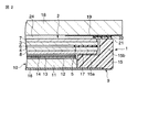
図1〜図8はこの発明の一実施例を示しており、図1は製造された保護板一体型表示モジュールの断面図、図2は前記保護板一体型表示モジュールの一端部の拡大断面図である。 1 to 8 show an embodiment of the present invention. FIG. 1 is a sectional view of a manufactured protection plate integrated display module, and FIG. 2 is an enlarged sectional view of one end of the protection plate integrated display module. It is.
この保護板一体型表示モジュールは、画像を表示する表示パネル1の観察側に透明な観察面保護板18が配置され、前記表示パネル1と前記保護板18との間の間隙が透明な充填層24により充填されたものである。
In this protection plate integrated display module, a transparent observation
前記表示パネル1は、液晶表示素子2と、前記液晶表示素子2の観察側とは反対側の面に対向させて配置され、前記液晶表示素子2に向けて照明光を照射する面光源ユニット9とにより構成されている。
The
前記液晶表示素子2は、図2のように、予め定めた間隙を設けて対向配置され、画面エリア(図示せず)を囲む枠状のシール材5を介して接合された観察側とその反対側の一対の透明基板3,4と、これらの基板3,4間の間隙の前記シール材5で囲まれた領域に封入された液晶層6と、前記一対の基板3,4の外面にそれぞれ配置された観察側とその反対側の一対の偏光板7,8とからなっている。
As shown in FIG. 2, the liquid
この液晶表示素子2は、例えばTFT(薄膜トランジスタ)をアクティブ素子としたアクティブマトリックス液晶表示素子であり、図では省略しているが、一方の基板、例えば観察側とは反対側の基板4の内面に、行方向及び列方向にマトリックス状に配列させて形成された複数の透明な画素電極と、これらの画素電極にそれぞれ対応させて配置され、対応する画素電極に接続された複数のTFTと、各行のTFTにゲート信号を供給する複数の走査線と、各列のTFTにデータ信号を供給する複数の信号線とが設けられ、他方の基板、例えば観察側の基板3の内面に、前記複数の画素電極の配列領域に対向する一枚膜状の透明な対向電極が設けられている。
The liquid
なお、図では省略しているが、前記観察側基板3の内面には、前記複数の画素電極と対向電極とが互いに対向する領域からなる複数の画素にそれぞれ対応させて、赤、緑、青の3色のカラーフィルタが設けられており、前記対向電極は、前記カラーフィルタの上に形成されている。また、前記一対の基板3,4の内面には、前記電極を覆って配向膜が設けられており、前記液晶層6の液晶分子は、前記一対の基板3,4間において、前記配向膜により規定される配向状態に配向している。
Although not shown in the figure, the inner surface of the observation-
また、前記面光源ユニット9は、図2のように、前記液晶表示素子2に向けて照明光を照射する面光源10と、前記面光源10を支持する面光源支持フレーム15とからなっている。
Further, as shown in FIG. 2, the surface
前記面光源10は、板状の透明部材からなり、その一端面(図示せず)に光を入射させる入射端面が形成され、2つの板面の一方に前記入射端面から入射した光を出射させる出射面が形成され、他方の板面に前記入射端面から入射した光を前記出射面に向けて内面反射する反射面が形成された導光板11と、前記導光板11の入射端面に対向させて配置された図示しない複数の発光素子(例えば発光ダイオード)と、前記導光板11の出射面上に設けられ、前記導光板11からの出射光を拡散させる拡散層12と、前記拡散層12の上に互いに重ねて配置された一対のプリズムシート13,14とからなっている。
The
なお、図2では前記プリズムシート13,14をそれぞれ一枚膜のように示しているが、これらのプリズムシート13,14の一方、例えば前記拡散層12側のプリズムシート13には、前記導光板11の幅方向(入射端面と平行な方向)と平行な複数の細長プリズムが密なピッチで形成され、他方のプリズムシート14には、前記導光板11の長手方向と平行な複数の細長プリズムが密なピッチで形成されており、前記導光板11の出射面から出射し、前記拡散層12により拡散された光は、前記一対のプリズムシート13,14により前記導光板11の出射面の法線方向に対する角度が小さくなる方向に屈折され、前記法線方向、つまり正面方向の出射光強度が高い強度分布の照明光となって出射する。
In FIG. 2, the
また、前記面光源支持フレーム15は、合成樹脂からなる成形品であり、前記液晶表示素子2の観察側とは反対側の面の周縁部に対応する矩形枠状の底枠部15aと、前記底枠部15aの外周部に形成された周壁部15bとからなっている。
The surface light
さらに、前記面光源支持フレーム15の前記液晶表示素子2が配置される側とは反対側の面には、前記面光源10の導光板11の反射面からの漏れ光を反射して前記導光板11に前記反射面から再入射させるための反射板16が、その外周部を前記底枠部15aの外面に一体的に固定して設けられている。
Further, the
前記面光源10は、前記面光源支持フレーム15の底枠部15aで囲まれたスペースに配置され、前記導光板11の反射面を前記反射板16に透明な接着材または両面粘着フィルムにより貼付けられている。
The
そして、前記液晶表示素子2は、前記面光源支持フレーム15内の前記周壁部15bで囲まれたスペースに配置され、前記観察側とは反対側の面(反対側の偏光板8の外面)の周縁部を、前記面光源支持フレーム15の底枠部15aに支持されるとともに、前記観察側とは反対側の面の周縁部を、前記面光源支持フレーム15の底枠部15aに、両面粘着テープ17により貼付け固定されている。
The liquid
一方、前記観察面保護板18は、周縁部が前記表示パネル1の外方に張出す大きさの矩形板状に形成されたガラス板またはアクリル樹脂板等からなっており、この保護板18の前記表示パネル1に対向する面に、前記表示パネル1の液晶表示素子2の画面エリア外の領域に対応させて、遮光性塗料の印刷膜、或いはクロム等の金属のメッキまたは蒸着膜からなる遮光膜19が形成されている。
On the other hand, the observation
この保護板18は、前記表示パネル1の観察側に、前記表示パネル1の液晶表示素子2の観察側の面(観察側の偏光板7の外面)との間に予め定めた間隙を設けて配置されている。
The
前記表示パネル1の液晶表示素子2と前記保護板18との間隙は、前記表示パネル1の液晶表示素子2の画面エリアに対応する領域を囲んで設けられた予め定めた厚さのスペーサ21により規定されている。
The gap between the liquid
前記スペーサ21は、前記表示パネル1の液晶表示素子2の画面エリアに対応する領域を囲む矩形枠状に形成され、且つ少なくとも一部に前記領域内と外部とを連通させるための欠落部22(図5参照)が設けられた樹脂フィルムからなっており、前記表示パネル1と前記保護板18の対向面のいずれか一方、例えば前記保護板18の表示パネル対向面の上に両面粘着テープ28により貼付けられ、前記対向面の他方、つまり前記表示パネル1の保護板対向面に当接されている。
The
なお、この実施例では、前記表示パネル1を、液晶表示素子2の観察側の面と面光源支持フレーム15の周壁部15bの頂面とが面一になるように設計し、前記スペーサ21を前記液晶表示素子2の周縁部から前記面光源支持フレーム15の周壁部15bの外周縁付近にわたる幅に形成することにより、前記スペーサ21を、前記液晶表示素子2の観察側の面の周縁部及び前記面光源支持フレーム15の周壁部15bの頂面に当接させている。
In this embodiment, the
そして、前記充填層24は、前記液晶パネル1と前記保護板18との間の間隙の前記スペーサ21で囲まれた領域に、光の照射、より具体的には、紫外線(以下、UVと記す)によって重合する光重合性(以下、UV重合性と記す)、或いはUV重合性と加熱により重合する熱重合性の両方の特性もった樹脂からなる充填材を充填し、この充填材の層をUV照射により、あるいはUV照射と加熱の両方により重合させて形成されている。なお、この実施例では、前記充填層24を、UV重合性と熱重合性の両方の特性もった樹脂からなる充填材により形成している。
The filling
前記UV重合性と熱重合性の両方の特性もった樹脂は、アクリレート、メタクリレート等のアクリル系モノマー、或いは、アクリレートとメタクリレートの一方または両方の低重合体であるアクリルオリゴマー等の脂環状エポキシ樹脂に、スルホニウム塩等の有機過酸化物からなる硬化開始剤を添加することにより得られる。 The resin having both the UV polymerizable property and the thermally polymerizable property is an alicyclic epoxy resin such as an acrylic monomer such as acrylate or methacrylate, or an acrylic oligomer that is a low polymer of one or both of acrylate and methacrylate. It can be obtained by adding a curing initiator comprising an organic peroxide such as a sulfonium salt.
この樹脂は、未重合状態における粘度が、1500〜10000mPa・s(ミリパスカル・セカント)、好ましくは3000〜5000mPa・sで、UV重合及び熱重合後のEコード硬度が、E4〜E13、好ましくはE7〜E10、UV重合及び熱重合による収縮率が、0.9〜2.0%、好ましくは0.97〜1.64%の特性を有するものが望ましい。 This resin has a viscosity in an unpolymerized state of 1500 to 10000 mPa · s (millipascal Secant), preferably 3000 to 5000 mPa · s, and an E code hardness after UV polymerization and thermal polymerization of E4 to E13, preferably It is desirable that the shrinkage rate due to E7 to E10, UV polymerization and thermal polymerization is 0.9 to 2.0%, preferably 0.97 to 1.64%.
図3は前記保護板一体型表示モジュールの製造工程図であり、この保護板一体型表示モジュールは、次のような工程で製造する。 FIG. 3 is a manufacturing process diagram of the protective plate-integrated display module. The protective plate-integrated display module is manufactured by the following process.
まず、図3の工程A1のように、前記保護板18の表示パネル対向面に前記スペーサ21を両面粘着テープ28により貼付け、図3の工程B1のように、前記表示パネル1の液晶表示素子2の観察側の面の画面エリアに対応する領域の上に、前記UV重合性と熱重合性の両方の特性もった樹脂からなる充填材24a(図6参照)を、転写印刷またはディスペンサ等によって供給する。
First, as shown in step A1 of FIG. 3, the
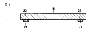
図4及び図5は前記スペーサ21が貼付けられた観察面保護板18の断面図及びスペーサ貼付け面側から見た平面図であり、この実施例では、前記スペーサ21を、前記画面エリアに対応する領域を囲む矩形枠状に形成し、その4つの角部にそれぞれ前記領域内と外部とを連通させるための欠落部22を形成している。
4 and 5 are a sectional view of the observation
次に、図3の工程C1のように、前記表示パネル1と前記保護板18とを重ね合わせて加圧し、前記スペーサ21を前記表示パネル1の保護板対向面(液晶表示素子2の観察側の面の周縁部及び面光源支持フレーム15の周壁部15bの頂面)に当接させるとともに、前記充填材24aを前記表示パネル1の表示素子2と前記保護板との間の間隙の前記スペーサ21で囲まれた領域に押し広げ、前記表示パネル1と前記保護板18とを図示しない冶具により前記加圧状態、つまり前記保護板18に貼付けられたスペーサ21を前記表示パネル1の保護板対向面に当接させた状態に保持する。
Next, as in step C1 of FIG. 3, the
なお、前記表示パネル1と前記保護板18の重ね合わせ及び加圧は、平板状の基台プレート上に前記表示パネル1を載置し、この表示パネル1の上に前記保護板18を位置決めして重ねた後に、前記保護板18の上に平板状の透明な加圧プレートを重ね、この加圧プレートを、エアーシリンダ等により、前記充填材24aの層と前記液晶表示素子2及び保護板18との接触面間に空気が閉じ込まれて気泡を発生することが無いように加圧速度を制御して加圧することにより行い、その後に、前記基台プレートと加圧プレートとを図示しない冶具によりクランプすることにより、前記加圧状態を保持する。
The
図6は前記表示パネル1と前記保護板18とを重ね合わせて加圧した状態の断面図であり、前記表示パネル1の液晶表示素子2上に供給された前記充填材24aは、その上に前記保護板18を重ねて加圧することにより、前記液晶表示素子2と前記保護板18との間の間隙内の空気を前記スペーサ21に設けられた欠落部22から外部に排出しながら押し広げられ、前記間隙の前記スペーサ21で囲まれた領域全体に充填される。
FIG. 6 is a cross-sectional view showing a state where the
この実施例では、前記スペーサ21を、前記液晶表示素子2の画面エリアに対応する領域を囲む矩形枠状に形成し、このスペーサ21の4つの角部にそれぞれ前記欠落部22を設けているため、前記液晶表示素子2と前記保護板18との間の間隙内の空気を前記4つの角部の欠落部22から排出し、前記充填材24aを、前記スペーサ21で囲まれた領域の全周方向に押し広げ、前記領域の略全域に均等に充填することができる。
In this embodiment, the
次に、図3の工程C2のように、前記冶具によりクランプされた前記基台プレートと加圧プレートとの間に挟持された前記表示パネル1と保護板18との重ね合わせ体に対して、前記保護板18の外面側、つまり前記保護板18の外面に当接された前記加圧プレートの外面側から、前記スペーサ21で囲まれた領域内の予め定めた部分に、スポット式UV照射装置によりUVを照射し、前記充填材24aの層を部分的にUV重合させる。
Next, as shown in Step C2 of FIG. 3, the stacked body of the
図7は前記充填材24aの層を部分的にUV重合させた状態の断面図、図8は部分的にUV重合された前記充填材24aの層の平面図であり、図において、24bは、UV重合した充填材を示している。
FIG. 7 is a cross-sectional view of a state in which the layer of the
この実施例では、図7及び図8のように、前記充填材24aの層の部分的なUV重合を、前記スペーサ21で囲まれた領域の中央部にスポット的にUVを照射することにより行い、前記充填材24aの層のうちの前記領域の中央部の充填材24aをUV重合させている。
In this embodiment, as shown in FIGS. 7 and 8, partial UV polymerization of the layer of the
このように、前記充填材24aの層を部分的にUV重合させることにより、前記表示パネル1の液晶表示素子2と前記保護板18とが、前記充填材24aの層のうちのUV重合した充填材24bによって部分的に仮接合される。
In this way, by partially UV-polymerizing the layer of the
前記充填材24aの層の一部を重合させた後は、図3の工程C3のように、前記冶具を外し、前記基台プレートと加圧プレートのうちの少なくとも前記保護板18の外面に当接された加圧プレートを取外すことができる。なお、前記基台プレートは、取外しても、そのまま前記表示パネル1と保護板18との重ね合わせ体の支持台として利用してもよい。
After polymerizing a part of the layer of the
このときは、前記表示パネル1の液晶表示素子2と前記保護板18とが、前記充填材24aの層のうちのUV重合した充填材24bにより部分的に接合されているため、前記冶具を外して前記加圧状態を解除しても、前記表示パネル1と前記保護板18との間隙が、前記スペーサ21によって規定された間隙に保たれる。
At this time, since the liquid
次に、図3の工程C4のように、前記表示パネル1と保護板18との重ね合わせ体を清浄雰囲気内に放置し、前記スペーサ21で囲まれた領域全体への未重合充填材24aの広がりを待つ。
Next, as in step C4 of FIG. 3, the superposed body of the
次に、図3の工程C5のように、前記保護板18の外面に加圧エアーを吹付けるエアー脱泡により、未重合充填材24a中の気泡を前記スペーサ21の前記欠落部22から排出し、その後に、図3の工程C6のように、前記保護板18の外面側から少なくとも前記スペーサ21で囲まれた領域全体にUVを照射し、前記充填材24aの層全体をUV重合させて図1及び図2のような充填層24を形成する。
Next, as shown in step C5 of FIG. 3, bubbles in the
このように、前記充填材24aの層全体をUV重合させると、前記表示パネル1の液晶表示素子2と前記保護板18とが、前記スペーサ21で囲まれた領域全体において前記UV重合した充填材24bからなる充填層24により接合される。
As described above, when the entire layer of the
次に、図3の工程C7のように、前記表示パネル1と保護板18との重ね合わせ体を、前記充填材24aの熱重合温度以上に保たれた加熱雰囲気内に一定時間放置し、前記充填材24aの層全体をUV重合させた前記充填層24を、前記充填材24aの熱重合温度以上に加熱することにより、前記充填材24aの層のうちの前記UV照射による重合不足部や未重合部を熱重合させ、前記表示モジュールを完成する。
Next, as in step C7 of FIG. 3, the superposed body of the
すなわち、前記充填材24aのUV重合においては、前記保護板18の外面側から照射されたUVが、前記保護板18の表示パネル対向面の外周部に形成された遮光膜19により遮られ、また、前記保護板18に装飾等のための印刷が施されている場合は、その印刷膜によっても前記UVが遮られるため、前記充填材24aの層全体をUV重合させて形成された前記充填層24の前記遮光膜19や印刷膜に対応する部分に、重合不足部や未重合部が残るが、このUV照射による重合不足部や未重合部は、前記充填材24aの重合温度以上に加熱することによって熱重合され、前記充填材14aの層全体がむら無く重合した充填層24が形成される。
That is, in the UV polymerization of the
上記製造方法は、前記保護板18の表示パネル対向面の上に、前記表示パネル1の液晶表示素子2の画面エリアに対応する領域を囲んで、予め定めた厚さのスペーサ21を貼付ける工程と、
前記表示パネル1の保護板対向面(液晶表示素子2の観察側の面)の前記画面エリアに対応する領域の上に、光の照射によって重合する樹脂、つまりUV重合性をもった樹脂からなる充填材24aを供給する工程と、
前記表示パネル1と前記保護板18とを重ね合わせて加圧し、前記スペーサ21を前記表示パネル1の保護板対向面に当接させるとともに、前記充填材24aを前記表示パネル1と前記保護板18との間の間隙の前記スペーサ21で囲まれた領域に押し広げ、前記表示パネル1と前記保護板18とを前記加圧状態に保持する工程と、
前記保護板18の外面側から前記スペーサ21で囲まれた領域内の予め定めた部分にUVを照射して、前記充填材24aの層を部分的にUV重合させる工程と、
前記スペーサ21で囲まれた領域全体へ未重合の前記充填材24aを広がらせる工程と、 前記保護板18の外面側から少なくとも前記スペーサ21で囲まれた領域全体にUVを照射して、前記充填材24aの層全体をUV重合させて前記充填層24を形成する工程とを備えるため、前記表示パネル1と前記保護板18とを樹脂により接合させた保護板一体型表示モジュールを製造することができる。
In the manufacturing method, a
On the area corresponding to the screen area of the surface facing the protective plate of the display panel 1 (the surface on the viewing side of the liquid crystal display element 2), it is made of a resin that is polymerized by light irradiation, that is, a resin having UV polymerizability. Supplying a
The
Irradiating a predetermined portion in a region surrounded by the
Spreading the
すなわち、上記製造方法は、前記保護板18の表示パネル対向面の上に前記スペーサ21を貼付け、前記表示パネル1の保護板対向面上に前記充填材24aを供給した後、前記表示パネル1と前記保護板18とを重ね合わせて加圧することにより、前記スペーサ21を前記表示パネル1の保護板対向面に当接させるとともに、前記充填材24aを前記表示パネル1と前記保護板18との間の間隙の前記スペーサ21で囲まれた領域に押し広げ、この充填材24aの層をUV重合させて前記表示パネル1と前記保護板18との間の間隙を充填する充填層24を形成しているため、前記表示パネル1の液晶表示素子2と前記保護板18とを、前記スペーサ21で囲まれた領域全体において、前記樹脂からなる充填層24により充分な強度で接合することができる。
That is, in the manufacturing method, the
また、上記製造方法は、前記表示パネル1と前記保護板18との間の間隙の前記スペーサ21で囲まれた領域に充填された充填材24aを、まず前記スペーサ21で囲まれた領域内の予め定めた部分にUVを照射して部分的にUV重合させ、その後に、少なくとも前記スペーサ21で囲まれた領域全体にUVを照射して前記充填材24aの層全体をUV重合させるため、重ね合わせて加圧された前記表示パネル1と前記保護板18との冶具により加圧状態の保持時間は、前記部分的なUV重合が終了するまでの短い時間でよく、その後は前記冶具を用いる必要が無いため、前記保護板一体型表示モジュールを容易に製造することができる。
In the manufacturing method, the filling
しかも、上記製造方法は、前記表示パネル1の保護板対向面上に、UV重合性と熱重合性の両方の特性もった樹脂からなる充填材24aを供給し、前記充填材24aの層全体をUV重合させた後、前記充填材24aの熱重合温度以上に加熱するため、前記充填材24aの層全体をUV重合させて形成された前記充填層24の重合不足部や未重合部を熱重合させ、前記充填材14aの層全体がむら無く重合した良好な品質の充填層24を形成することができる。
In addition, the above manufacturing method supplies the
そして、前記充填材24aの層全体をUV重合させて形成され、さらに前記UV照射による重合不足部や未重合部を熱重合された前記充填層24は、ゴム層のような適度な弾性を有しているため、前記保護板18の外面に衝撃が加わったときに、その衝撃を前記充填層24により緩衝し、前記表示パネル1を前記衝撃から保護することができる。
The
なお、上記実施例の製造方法では、前記表示パネル1と前記保護板18との間の間隙に充填された充填材24aの層の部分的UV重合を、前記スペーサ21で囲まれた領域の中央部にスポット的にUVを照射することにより行っているが、前記充填材24aの層の部分的UV重合は、他の部分にUVを照射することにより行ってもよい。
In the manufacturing method of the above embodiment, the partial UV polymerization of the layer of the
図9〜図12はそれぞれ前記充填材24aの層の他の部分的UV重合例を示しており、図9に示した部分的UV重合例は、前記スペーサ21で囲まれた領域の中央部の予め定めた長さの部分に、UVを、前記部分の長さ方向に連続的に移動させて照射する例であり、このような部分的UV重合を行うことにより、前記表示パネル1と前記保護板18との部分的な仮接合の安定性を高くすることができる。
FIGS. 9 to 12 each show another partial UV polymerization example of the layer of the
図10に示した部分的UV重合例は、前記スペーサ21で囲まれた領域の中央部の複数箇所、例えば2箇所にスポット的にUVを照射する例であり、このような部分的UV重合を行うことにより、前記表示パネル1と前記保護板18との部分的な仮接合の安定性を高くすることができる。
The partial UV polymerization example shown in FIG. 10 is an example in which UV is irradiated in a spot manner at a plurality of, for example, two places in the central portion of the region surrounded by the
図11に示した部分的UV重合例は、前記スペーサ21で囲まれた領域の4隅部にスポット的にUVを照射する例であり、このような部分的UV重合を行うことにより、前記表示パネル1と前記保護板18との部分的な仮接合の安定性を高くすることができる。
The partial UV polymerization example shown in FIG. 11 is an example in which UV is irradiated in a spot manner to the four corners of the region surrounded by the
図12に示した部分的UV重合例は、前記スペーサ21で囲まれた領域の中央部と4隅部にスポット的にUVを照射する例であり、このような部分的UV重合を行うことにより、前記表示パネル1と前記保護板18との部分的な仮接合の安定性をさらに高くすることができる。
The partial UV polymerization example shown in FIG. 12 is an example in which UV is applied in a spot manner to the central portion and the four corners of the region surrounded by the
なお、上記実施例の製造方法では、前記充填層24を、UV重合性と熱重合性の両方の特性もった樹脂からなる充填材24aにより形成しているが、充填材の充填領域全体にUVを照射できる場合は、前記表示パネル1と観察面保護板18との間の間隙の前記スペーサ21で囲まれた領域にUV重合性樹脂からなる充填材を充填し、その充填材層の重合をUV照射のみで行ってもよい。
In the manufacturing method of the above embodiment, the filling
また、上記実施例の製造方法では、前記保護板18の表示パネル対向面に前記スペーサ21を貼付け、前記表示パネル1の保護板対向面の画面エリアに対応する領域の上に前記充填材24aを供給しているが、前記表示パネル1の保護板対向面に前記スペーサ21を貼付け、前記保護板18の表示パネル対向面の前記画面エリアに対応する領域の上に前記充填材24aを供給してもよく、さらに、前記表示パネル1と前記保護板18の対向面のいずれか一方の上に前記スペーサ21を貼付け、前記スペーサ21を貼付けた面の前記画面エリアに対応する領域の上に前記充填材24aを供給してもよい。
Moreover, in the manufacturing method of the said Example, the said
さらに、上記実施例の製造方法では、前記スペーサ21を、前記表示パネル1の液晶表示素子2の周縁部から面光源支持フレーム15の周壁部15bの外周縁付近にわたる幅に形成しているが、このスペーサ21は、前記液晶表示素子2の周縁部に対応する幅に形成してもよい。
Further, in the manufacturing method of the above embodiment, the
また、この発明の製造方法は、液晶表示素子2と面光源ユニット9とからなる表示パネル1の観察側に観察面保護板18を配置した保護板一体型表示モジュールに限らず、液晶表示素子2のみからなる表示パネルの観察側に観察面保護板18を配置した保護板一体型表示モジュールや、エレクトロルミネッセンス表示素子やプラズマ表示素子等の自発光型表示素子からなる表示パネルの観察側に観察面保護板18を配置した保護板一体型表示モジュールの製造にも適用することができる。
The manufacturing method of the present invention is not limited to the protection plate integrated display module in which the observation
1…表示パネル、2…液晶表示素子、9…面光源ユニット、10…面光源、15…面光源支持フレーム、17…両面粘着テープ、18…観察面保護板、19…遮光膜、21…スペーサ、22…欠落部、23…両面粘着テープ、24…充填層、24a…充填材、24b…UV重合した充填材。
DESCRIPTION OF
Claims (9)
前記表示パネルの前記保護板との対向面及び前記保護板の前記表示パネルとの対向面のうち何れか一方の対向面に、前記表示パネルの画面エリアに対応する領域を囲むように、スペーサを貼付ける工程と、
次いで、前記表示パネル及び前記保護板のうち何れか一方の、前記画面エリアに対応する領域上に光の照射によって重合する樹脂からなる充填材を供給する工程と、
次いで、前記保護板及び前記表示パネルを加圧することによって前記保護板及び前記表示パネルの前記各対向面に前記スペーサを当接させる工程と、
次いで、前記加圧状態を保持しながら、前記スペーサで囲まれた領域内の予め定めた部分に光を照射して前記充填材を部分的に重合させる工程と、
次いで、前記加圧状態を解除して、前記保護板及び前記表示パネルを放置し、前記スペーサで囲まれた領域全体への未重合充填材の広がりを待つ工程と、
次いで、前記加圧状態が解除された状態で、前記スペーサで囲まれた領域全体に光を照射して前記充填材全体を重合させる工程と、
を備えることを特徴とする保護板一体型表示モジュールの製造方法。 In the manufacturing method of a protection plate integrated display module in which a protection plate is disposed on a display panel for displaying an image,
A spacer is provided on either one of the facing surface of the display panel facing the protection plate and the facing surface of the protection plate facing the display panel so as to surround a region corresponding to the screen area of the display panel. Pasting process,
Next, a step of supplying a filler made of a resin that is polymerized by light irradiation on a region corresponding to the screen area of either the display panel or the protective plate;
Next, pressurizing the protective plate and the display panel to bring the spacer into contact with the opposing surfaces of the protective plate and the display panel;
Next, while maintaining the pressurized state, irradiating light to a predetermined portion in the region surrounded by the spacer to partially polymerize the filler,
Next, releasing the pressure state, leaving the protective plate and the display panel, and waiting for the unpolymerized filler to spread over the entire region surrounded by the spacers;
Next, in a state where the pressurized state is released, irradiating the entire region surrounded by the spacer to polymerize the entire filler, and
A manufacturing method of a protection plate integrated display module, comprising:
前記未重合充填材の広がりを待つ工程の後、前記充填材全体を重合させる工程の前に、前記保護板の外面に加圧エアーを吹付けるエアー脱泡により、前記未重合充填材中の気泡を前記スペーサの前記欠落部から排出する工程を、さらに備える請求項1に記載の保護板一体型表示モジュールの製造方法。 The spacer is provided so as to have a missing portion for communicating the inside and outside of the screen area of the display panel,
After the step of waiting for the unpolymerized filler to spread, before the step of polymerizing the entire filler, bubbles in the unpolymerized filler are obtained by air defoaming that blows pressurized air on the outer surface of the protective plate. The manufacturing method of the protection plate integrated display module according to claim 1, further comprising a step of discharging the liquid crystal from the missing portion of the spacer.
Priority Applications (1)
| Application Number | Priority Date | Filing Date | Title |
|---|---|---|---|
| JP2007283551A JP5374858B2 (en) | 2007-10-31 | 2007-10-31 | Method for manufacturing protective plate integrated display module |
Applications Claiming Priority (1)
| Application Number | Priority Date | Filing Date | Title |
|---|---|---|---|
| JP2007283551A JP5374858B2 (en) | 2007-10-31 | 2007-10-31 | Method for manufacturing protective plate integrated display module |
Publications (3)
| Publication Number | Publication Date |
|---|---|
| JP2009109855A JP2009109855A (en) | 2009-05-21 |
| JP2009109855A5 JP2009109855A5 (en) | 2010-12-09 |
| JP5374858B2 true JP5374858B2 (en) | 2013-12-25 |
Family
ID=40778382
Family Applications (1)
| Application Number | Title | Priority Date | Filing Date |
|---|---|---|---|
| JP2007283551A Expired - Fee Related JP5374858B2 (en) | 2007-10-31 | 2007-10-31 | Method for manufacturing protective plate integrated display module |
Country Status (1)
| Country | Link |
|---|---|
| JP (1) | JP5374858B2 (en) |
Families Citing this family (21)
| Publication number | Priority date | Publication date | Assignee | Title |
|---|---|---|---|---|
| KR101058730B1 (en) | 2007-09-28 | 2011-08-22 | 가시오게산키 가부시키가이샤 | Display element with integral protective plate and display device using same |
| JP4666068B2 (en) | 2008-12-11 | 2011-04-06 | カシオ計算機株式会社 | Protective plate integrated liquid crystal display panel and manufacturing method thereof |
| JP4905485B2 (en) | 2009-03-13 | 2012-03-28 | カシオ計算機株式会社 | Protection plate integrated display device |
| KR101130431B1 (en) | 2009-03-13 | 2012-03-28 | 가시오게산키 가부시키가이샤 | Protective plate integrated display apparatus |
| JP4821877B2 (en) | 2009-03-27 | 2011-11-24 | カシオ計算機株式会社 | Protection plate integrated liquid crystal display panel and electronic device |
| JP5652807B2 (en) * | 2009-06-11 | 2015-01-14 | レノボ・イノベーションズ・リミテッド(香港) | Backlight type display device for portable device |
| JP2011067802A (en) * | 2009-09-28 | 2011-04-07 | Origin Electric Co Ltd | Method and apparatus for manufacturing joining member |
| JP5487915B2 (en) * | 2009-11-30 | 2014-05-14 | カシオ計算機株式会社 | Protective plate integrated type liquid crystal display panel manufacturing method |
| JP5550357B2 (en) * | 2010-01-15 | 2014-07-16 | 株式会社ジャパンディスプレイ | Display device with front window |
| JP5938858B2 (en) * | 2011-07-27 | 2016-06-22 | 三菱電機株式会社 | Display device |
| JP4981190B1 (en) * | 2011-12-08 | 2012-07-18 | 信越エンジニアリング株式会社 | Manufacturing method of bonding device |
| WO2013179815A1 (en) * | 2012-05-29 | 2013-12-05 | シャープ株式会社 | Display device |
| JP5612043B2 (en) * | 2012-09-03 | 2014-10-22 | オリジン電気株式会社 | Bonding member manufacturing method and bonding member manufacturing apparatus |
| DE102013226547B4 (en) * | 2013-12-18 | 2015-10-01 | Continental Automotive Gmbh | Method for producing a display unit and display unit |
| JP5908546B2 (en) * | 2014-08-18 | 2016-04-26 | レノボ・イノベーションズ・リミテッド(香港) | Backlight type display device for portable device |
| WO2018146953A1 (en) * | 2017-02-07 | 2018-08-16 | デクセリアルズ株式会社 | Method for manufacturing image display device |
| JP7143100B2 (en) * | 2018-03-26 | 2022-09-28 | フォルシアクラリオン・エレクトロニクス株式会社 | DISPLAY DEVICE AND METHOD FOR MANUFACTURING DISPLAY DEVICE |
| CN111580297A (en) * | 2020-06-30 | 2020-08-25 | 北京小米移动软件有限公司 | Display module and manufacturing method thereof |
| CN112652243B (en) * | 2020-12-09 | 2022-11-11 | 深圳一鑫新材料有限公司 | Four-side curved display screen laminating process |
| CN112652242B (en) * | 2020-12-09 | 2022-08-23 | 深圳一鑫新材料有限公司 | Flexible curved surface display screen laminating process |
| CN112652244B (en) * | 2020-12-09 | 2022-11-11 | 深圳一鑫新材料有限公司 | Four-side curved display screen laminating process |
Family Cites Families (8)
| Publication number | Priority date | Publication date | Assignee | Title |
|---|---|---|---|---|
| JPH075446A (en) * | 1993-04-22 | 1995-01-10 | Matsushita Electric Ind Co Ltd | Production of liquid crystal panel |
| JP4113730B2 (en) * | 2002-05-31 | 2008-07-09 | オプトレックス株式会社 | Method for stacking liquid crystal display panels |
| JP2005055641A (en) * | 2003-08-04 | 2005-03-03 | Yokogawa Electric Corp | Liquid crystal display device |
| JP2006189715A (en) * | 2005-01-07 | 2006-07-20 | Pentax Corp | Protective cover for display panel, and its use |
| JP2007033537A (en) * | 2005-07-22 | 2007-02-08 | Sharp Corp | Apparatus for manufacturing flexible display element and method for manufacturing the element |
| JP2007226083A (en) * | 2006-02-27 | 2007-09-06 | Epson Imaging Devices Corp | Method and apparatus for manufacturing electro-optic device |
| JP2007248696A (en) * | 2006-03-15 | 2007-09-27 | Epson Imaging Devices Corp | Method for manufacturing electrooptical device |
| JP2007264308A (en) * | 2006-03-28 | 2007-10-11 | Optrex Corp | Method of laminating plate member |
-
2007
- 2007-10-31 JP JP2007283551A patent/JP5374858B2/en not_active Expired - Fee Related
Also Published As
| Publication number | Publication date |
|---|---|
| JP2009109855A (en) | 2009-05-21 |
Similar Documents
| Publication | Publication Date | Title |
|---|---|---|
| JP5374858B2 (en) | Method for manufacturing protective plate integrated display module | |
| JP4636066B2 (en) | Liquid crystal display device | |
| KR101027219B1 (en) | Method for Manufacturing a Display Device | |
| JP4462317B2 (en) | Protection plate integrated display panel | |
| US20090283211A1 (en) | Method of Manufacturing a Display Device and Bonding Method | |
| JP4983891B2 (en) | Manufacturing method of display panel integrated display panel | |
| US6830947B2 (en) | Method for manufacturing liquid crystal display panel | |
| KR20140089014A (en) | Display device and manufacturing method thereof | |
| JP6621937B2 (en) | Image display device and method of manufacturing image display device | |
| JP2008040144A (en) | Display device | |
| CN102109716A (en) | Method of fabricating liquid crystal display device | |
| JP7442471B2 (en) | Method for manufacturing laminate | |
| KR20180079096A (en) | Flexible adhesive tape and dispaly device usign the same | |
| US20140057519A1 (en) | Curing device and method for curing frame of liquid crystal panel | |
| JP2010176111A (en) | Protective plate for flat panel display | |
| JP5664076B2 (en) | Electronic member with protective plate and method for manufacturing electronic member with protective plate | |
| KR20080029551A (en) | Liquid crystal display device | |
| JP5315965B2 (en) | Protective plate integrated display panel and manufacturing method thereof | |
| JP2008268420A (en) | Method for manufacturing liquid crystal display device | |
| JP5125417B2 (en) | Protection plate integrated display panel | |
| KR100898047B1 (en) | Optical member and method of manufacturing the same | |
| KR20180001239A (en) | Optical sheet and method of manufacturing the same | |
| US10175416B2 (en) | Method of manufacturing a light guide plate and display apparatus including the same | |
| JP5309840B2 (en) | Protective plate integrated type liquid crystal display panel manufacturing method | |
| JP5088356B2 (en) | Manufacturing method of display panel integrated display panel |
Legal Events
| Date | Code | Title | Description |
|---|---|---|---|
| A521 | Written amendment |
Free format text: JAPANESE INTERMEDIATE CODE: A523 Effective date: 20101022 |
|
| A621 | Written request for application examination |
Free format text: JAPANESE INTERMEDIATE CODE: A621 Effective date: 20101022 |
|
| RD04 | Notification of resignation of power of attorney |
Free format text: JAPANESE INTERMEDIATE CODE: A7424 Effective date: 20120529 |
|
| A977 | Report on retrieval |
Free format text: JAPANESE INTERMEDIATE CODE: A971007 Effective date: 20120531 |
|
| A131 | Notification of reasons for refusal |
Free format text: JAPANESE INTERMEDIATE CODE: A131 Effective date: 20121009 |
|
| A521 | Written amendment |
Free format text: JAPANESE INTERMEDIATE CODE: A523 Effective date: 20121210 |
|
| A131 | Notification of reasons for refusal |
Free format text: JAPANESE INTERMEDIATE CODE: A131 Effective date: 20130402 |
|
| A521 | Written amendment |
Free format text: JAPANESE INTERMEDIATE CODE: A523 Effective date: 20130531 |
|
| A131 | Notification of reasons for refusal |
Free format text: JAPANESE INTERMEDIATE CODE: A131 Effective date: 20130618 |
|
| A521 | Written amendment |
Free format text: JAPANESE INTERMEDIATE CODE: A523 Effective date: 20130805 |
|
| TRDD | Decision of grant or rejection written | ||
| A01 | Written decision to grant a patent or to grant a registration (utility model) |
Free format text: JAPANESE INTERMEDIATE CODE: A01 Effective date: 20130827 |
|
| A61 | First payment of annual fees (during grant procedure) |
Free format text: JAPANESE INTERMEDIATE CODE: A61 Effective date: 20130909 |
|
| R150 | Certificate of patent or registration of utility model |
Free format text: JAPANESE INTERMEDIATE CODE: R150 |
|
| LAPS | Cancellation because of no payment of annual fees |