JP5364281B2 - Method for manufacturing semiconductor device - Google Patents
Method for manufacturing semiconductor device Download PDFInfo
- Publication number
- JP5364281B2 JP5364281B2 JP2008064627A JP2008064627A JP5364281B2 JP 5364281 B2 JP5364281 B2 JP 5364281B2 JP 2008064627 A JP2008064627 A JP 2008064627A JP 2008064627 A JP2008064627 A JP 2008064627A JP 5364281 B2 JP5364281 B2 JP 5364281B2
- Authority
- JP
- Japan
- Prior art keywords
- single crystal
- layer
- crystal semiconductor
- substrate
- oxide film
- Prior art date
- Legal status (The legal status is an assumption and is not a legal conclusion. Google has not performed a legal analysis and makes no representation as to the accuracy of the status listed.)
- Expired - Fee Related
Links
- 239000004065 semiconductor Substances 0.000 title claims abstract description 239
- 238000000034 method Methods 0.000 title claims abstract description 98
- 238000004519 manufacturing process Methods 0.000 title claims description 47
- 239000013078 crystal Substances 0.000 claims abstract description 228
- 239000010410 layer Substances 0.000 claims description 482
- 239000000758 substrate Substances 0.000 claims description 193
- VYPSYNLAJGMNEJ-UHFFFAOYSA-N Silicium dioxide Chemical compound O=[Si]=O VYPSYNLAJGMNEJ-UHFFFAOYSA-N 0.000 claims description 80
- 229910052814 silicon oxide Inorganic materials 0.000 claims description 77
- 150000002500 ions Chemical class 0.000 claims description 41
- 239000012790 adhesive layer Substances 0.000 claims description 33
- 239000001257 hydrogen Substances 0.000 claims description 29
- 229910052739 hydrogen Inorganic materials 0.000 claims description 29
- 238000010438 heat treatment Methods 0.000 claims description 26
- UFHFLCQGNIYNRP-UHFFFAOYSA-N Hydrogen Chemical compound [H][H] UFHFLCQGNIYNRP-UHFFFAOYSA-N 0.000 claims description 21
- 229910052736 halogen Inorganic materials 0.000 claims description 21
- 239000007789 gas Substances 0.000 claims description 19
- 150000002367 halogens Chemical class 0.000 claims description 19
- 238000005229 chemical vapour deposition Methods 0.000 claims description 17
- 238000005530 etching Methods 0.000 claims description 16
- 238000005468 ion implantation Methods 0.000 claims description 12
- 150000001282 organosilanes Chemical class 0.000 claims description 12
- 239000000969 carrier Substances 0.000 abstract description 13
- 239000010408 film Substances 0.000 description 153
- 235000012431 wafers Nutrition 0.000 description 146
- 239000012535 impurity Substances 0.000 description 33
- 229910052710 silicon Inorganic materials 0.000 description 31
- XUIMIQQOPSSXEZ-UHFFFAOYSA-N Silicon Chemical compound [Si] XUIMIQQOPSSXEZ-UHFFFAOYSA-N 0.000 description 30
- 239000010703 silicon Substances 0.000 description 30
- 229910052581 Si3N4 Inorganic materials 0.000 description 26
- HQVNEWCFYHHQES-UHFFFAOYSA-N silicon nitride Chemical compound N12[Si]34N5[Si]62N3[Si]51N64 HQVNEWCFYHHQES-UHFFFAOYSA-N 0.000 description 26
- 239000011229 interlayer Substances 0.000 description 24
- 229910052751 metal Inorganic materials 0.000 description 18
- 239000002184 metal Substances 0.000 description 18
- IJGRMHOSHXDMSA-UHFFFAOYSA-N Atomic nitrogen Chemical compound N#N IJGRMHOSHXDMSA-UHFFFAOYSA-N 0.000 description 16
- 230000008569 process Effects 0.000 description 16
- 239000000463 material Substances 0.000 description 15
- 238000012545 processing Methods 0.000 description 15
- 229910021332 silicide Inorganic materials 0.000 description 15
- FVBUAEGBCNSCDD-UHFFFAOYSA-N silicide(4-) Chemical compound [Si-4] FVBUAEGBCNSCDD-UHFFFAOYSA-N 0.000 description 15
- 230000000694 effects Effects 0.000 description 14
- 230000003647 oxidation Effects 0.000 description 14
- 238000007254 oxidation reaction Methods 0.000 description 14
- 238000011282 treatment Methods 0.000 description 13
- 230000015572 biosynthetic process Effects 0.000 description 12
- 239000010949 copper Substances 0.000 description 11
- 230000006870 function Effects 0.000 description 11
- 239000011521 glass Substances 0.000 description 11
- -1 hydrogen ions Chemical class 0.000 description 11
- RYGMFSIKBFXOCR-UHFFFAOYSA-N Copper Chemical compound [Cu] RYGMFSIKBFXOCR-UHFFFAOYSA-N 0.000 description 9
- QVGXLLKOCUKJST-UHFFFAOYSA-N atomic oxygen Chemical compound [O] QVGXLLKOCUKJST-UHFFFAOYSA-N 0.000 description 9
- 229910052802 copper Inorganic materials 0.000 description 9
- 229910021421 monocrystalline silicon Inorganic materials 0.000 description 9
- 239000001301 oxygen Substances 0.000 description 9
- 229910052760 oxygen Inorganic materials 0.000 description 9
- ZOXJGFHDIHLPTG-UHFFFAOYSA-N Boron Chemical compound [B] ZOXJGFHDIHLPTG-UHFFFAOYSA-N 0.000 description 8
- 229910052796 boron Inorganic materials 0.000 description 8
- 229910001385 heavy metal Inorganic materials 0.000 description 8
- 229910052757 nitrogen Inorganic materials 0.000 description 8
- 229910021426 porous silicon Inorganic materials 0.000 description 8
- 238000005498 polishing Methods 0.000 description 7
- VEXZGXHMUGYJMC-UHFFFAOYSA-N Hydrochloric acid Chemical compound Cl VEXZGXHMUGYJMC-UHFFFAOYSA-N 0.000 description 6
- MHAJPDPJQMAIIY-UHFFFAOYSA-N Hydrogen peroxide Chemical compound OO MHAJPDPJQMAIIY-UHFFFAOYSA-N 0.000 description 6
- 238000011109 contamination Methods 0.000 description 6
- 150000004767 nitrides Chemical class 0.000 description 6
- WQJQOUPTWCFRMM-UHFFFAOYSA-N tungsten disilicide Chemical compound [Si]#[W]#[Si] WQJQOUPTWCFRMM-UHFFFAOYSA-N 0.000 description 6
- 229910021342 tungsten silicide Inorganic materials 0.000 description 6
- 230000005684 electric field Effects 0.000 description 5
- 230000005669 field effect Effects 0.000 description 5
- 238000002161 passivation Methods 0.000 description 5
- 239000000126 substance Substances 0.000 description 5
- QGZKDVFQNNGYKY-UHFFFAOYSA-N Ammonia Chemical compound N QGZKDVFQNNGYKY-UHFFFAOYSA-N 0.000 description 4
- BOTDANWDWHJENH-UHFFFAOYSA-N Tetraethyl orthosilicate Chemical compound CCO[Si](OCC)(OCC)OCC BOTDANWDWHJENH-UHFFFAOYSA-N 0.000 description 4
- NRTOMJZYCJJWKI-UHFFFAOYSA-N Titanium nitride Chemical compound [Ti]#N NRTOMJZYCJJWKI-UHFFFAOYSA-N 0.000 description 4
- 230000001133 acceleration Effects 0.000 description 4
- 229910052782 aluminium Inorganic materials 0.000 description 4
- 229910052785 arsenic Inorganic materials 0.000 description 4
- RQNWIZPPADIBDY-UHFFFAOYSA-N arsenic atom Chemical compound [As] RQNWIZPPADIBDY-UHFFFAOYSA-N 0.000 description 4
- 229910052795 boron group element Inorganic materials 0.000 description 4
- 239000000460 chlorine Substances 0.000 description 4
- PMHQVHHXPFUNSP-UHFFFAOYSA-M copper(1+);methylsulfanylmethane;bromide Chemical compound Br[Cu].CSC PMHQVHHXPFUNSP-UHFFFAOYSA-M 0.000 description 4
- 229910000449 hafnium oxide Inorganic materials 0.000 description 4
- 238000002955 isolation Methods 0.000 description 4
- 229910052696 pnictogen Inorganic materials 0.000 description 4
- 238000007789 sealing Methods 0.000 description 4
- 238000000926 separation method Methods 0.000 description 4
- 239000005368 silicate glass Substances 0.000 description 4
- XLYOFNOQVPJJNP-UHFFFAOYSA-N water Chemical compound O XLYOFNOQVPJJNP-UHFFFAOYSA-N 0.000 description 4
- ZAMOUSCENKQFHK-UHFFFAOYSA-N Chlorine atom Chemical compound [Cl] ZAMOUSCENKQFHK-UHFFFAOYSA-N 0.000 description 3
- BLRPTPMANUNPDV-UHFFFAOYSA-N Silane Chemical compound [SiH4] BLRPTPMANUNPDV-UHFFFAOYSA-N 0.000 description 3
- 238000005411 Van der Waals force Methods 0.000 description 3
- 230000009471 action Effects 0.000 description 3
- XAGFODPZIPBFFR-UHFFFAOYSA-N aluminium Chemical compound [Al] XAGFODPZIPBFFR-UHFFFAOYSA-N 0.000 description 3
- 229910052801 chlorine Inorganic materials 0.000 description 3
- 238000000151 deposition Methods 0.000 description 3
- 238000013461 design Methods 0.000 description 3
- 238000010586 diagram Methods 0.000 description 3
- 238000009826 distribution Methods 0.000 description 3
- 238000005247 gettering Methods 0.000 description 3
- 239000012212 insulator Substances 0.000 description 3
- 230000001678 irradiating effect Effects 0.000 description 3
- 239000000203 mixture Substances 0.000 description 3
- 238000009832 plasma treatment Methods 0.000 description 3
- 238000007747 plating Methods 0.000 description 3
- 239000010453 quartz Substances 0.000 description 3
- 238000005001 rutherford backscattering spectroscopy Methods 0.000 description 3
- 229910000077 silane Inorganic materials 0.000 description 3
- 238000003860 storage Methods 0.000 description 3
- 230000017105 transposition Effects 0.000 description 3
- 229910016909 AlxOy Inorganic materials 0.000 description 2
- XKRFYHLGVUSROY-UHFFFAOYSA-N Argon Chemical compound [Ar] XKRFYHLGVUSROY-UHFFFAOYSA-N 0.000 description 2
- JBRZTFJDHDCESZ-UHFFFAOYSA-N AsGa Chemical compound [As]#[Ga] JBRZTFJDHDCESZ-UHFFFAOYSA-N 0.000 description 2
- 102100040844 Dual specificity protein kinase CLK2 Human genes 0.000 description 2
- KRHYYFGTRYWZRS-UHFFFAOYSA-N Fluorane Chemical compound F KRHYYFGTRYWZRS-UHFFFAOYSA-N 0.000 description 2
- 229910001218 Gallium arsenide Inorganic materials 0.000 description 2
- 101000749291 Homo sapiens Dual specificity protein kinase CLK2 Proteins 0.000 description 2
- GPXJNWSHGFTCBW-UHFFFAOYSA-N Indium phosphide Chemical compound [In]#P GPXJNWSHGFTCBW-UHFFFAOYSA-N 0.000 description 2
- OAICVXFJPJFONN-UHFFFAOYSA-N Phosphorus Chemical compound [P] OAICVXFJPJFONN-UHFFFAOYSA-N 0.000 description 2
- QAOWNCQODCNURD-UHFFFAOYSA-N Sulfuric acid Chemical compound OS(O)(=O)=O QAOWNCQODCNURD-UHFFFAOYSA-N 0.000 description 2
- XLOMVQKBTHCTTD-UHFFFAOYSA-N Zinc monoxide Chemical compound [Zn]=O XLOMVQKBTHCTTD-UHFFFAOYSA-N 0.000 description 2
- GDFCWFBWQUEQIJ-UHFFFAOYSA-N [B].[P] Chemical compound [B].[P] GDFCWFBWQUEQIJ-UHFFFAOYSA-N 0.000 description 2
- 229910021529 ammonia Inorganic materials 0.000 description 2
- 238000007743 anodising Methods 0.000 description 2
- 125000004429 atom Chemical group 0.000 description 2
- 230000004888 barrier function Effects 0.000 description 2
- 230000005540 biological transmission Effects 0.000 description 2
- 238000004364 calculation method Methods 0.000 description 2
- 239000003990 capacitor Substances 0.000 description 2
- 230000008859 change Effects 0.000 description 2
- 238000006243 chemical reaction Methods 0.000 description 2
- 229910052804 chromium Inorganic materials 0.000 description 2
- 239000011651 chromium Substances 0.000 description 2
- 239000010941 cobalt Substances 0.000 description 2
- 229910017052 cobalt Inorganic materials 0.000 description 2
- GUTLYIVDDKVIGB-UHFFFAOYSA-N cobalt atom Chemical compound [Co] GUTLYIVDDKVIGB-UHFFFAOYSA-N 0.000 description 2
- 238000004891 communication Methods 0.000 description 2
- 238000005520 cutting process Methods 0.000 description 2
- 238000005516 engineering process Methods 0.000 description 2
- 239000011152 fibreglass Substances 0.000 description 2
- WIHZLLGSGQNAGK-UHFFFAOYSA-N hafnium(4+);oxygen(2-) Chemical compound [O-2].[O-2].[Hf+4] WIHZLLGSGQNAGK-UHFFFAOYSA-N 0.000 description 2
- 230000001771 impaired effect Effects 0.000 description 2
- 239000007769 metal material Substances 0.000 description 2
- 229910021334 nickel silicide Inorganic materials 0.000 description 2
- RUFLMLWJRZAWLJ-UHFFFAOYSA-N nickel silicide Chemical compound [Ni]=[Si]=[Ni] RUFLMLWJRZAWLJ-UHFFFAOYSA-N 0.000 description 2
- 230000010355 oscillation Effects 0.000 description 2
- TWNQGVIAIRXVLR-UHFFFAOYSA-N oxo(oxoalumanyloxy)alumane Chemical compound O=[Al]O[Al]=O TWNQGVIAIRXVLR-UHFFFAOYSA-N 0.000 description 2
- BPUBBGLMJRNUCC-UHFFFAOYSA-N oxygen(2-);tantalum(5+) Chemical compound [O-2].[O-2].[O-2].[O-2].[O-2].[Ta+5].[Ta+5] BPUBBGLMJRNUCC-UHFFFAOYSA-N 0.000 description 2
- 229910052698 phosphorus Inorganic materials 0.000 description 2
- 239000011574 phosphorus Substances 0.000 description 2
- 238000005268 plasma chemical vapour deposition Methods 0.000 description 2
- 239000004033 plastic Substances 0.000 description 2
- 229920003023 plastic Polymers 0.000 description 2
- 229910021420 polycrystalline silicon Inorganic materials 0.000 description 2
- 229920002620 polyvinyl fluoride Polymers 0.000 description 2
- 239000010980 sapphire Substances 0.000 description 2
- 229910052594 sapphire Inorganic materials 0.000 description 2
- 239000000565 sealant Substances 0.000 description 2
- 239000003566 sealing material Substances 0.000 description 2
- 238000003892 spreading Methods 0.000 description 2
- 230000007480 spreading Effects 0.000 description 2
- 238000004544 sputter deposition Methods 0.000 description 2
- 229910001936 tantalum oxide Inorganic materials 0.000 description 2
- 238000012546 transfer Methods 0.000 description 2
- NXHILIPIEUBEPD-UHFFFAOYSA-H tungsten hexafluoride Chemical compound F[W](F)(F)(F)(F)F NXHILIPIEUBEPD-UHFFFAOYSA-H 0.000 description 2
- 229910017073 AlLi Inorganic materials 0.000 description 1
- 229910004261 CaF 2 Inorganic materials 0.000 description 1
- VYZAMTAEIAYCRO-UHFFFAOYSA-N Chromium Chemical compound [Cr] VYZAMTAEIAYCRO-UHFFFAOYSA-N 0.000 description 1
- 102100040862 Dual specificity protein kinase CLK1 Human genes 0.000 description 1
- 101000749294 Homo sapiens Dual specificity protein kinase CLK1 Proteins 0.000 description 1
- 229910017911 MgIn Inorganic materials 0.000 description 1
- NIXOWILDQLNWCW-UHFFFAOYSA-N acrylic acid group Chemical group C(C=C)(=O)O NIXOWILDQLNWCW-UHFFFAOYSA-N 0.000 description 1
- 230000004913 activation Effects 0.000 description 1
- 230000002411 adverse Effects 0.000 description 1
- 229910045601 alloy Inorganic materials 0.000 description 1
- 239000000956 alloy Substances 0.000 description 1
- 238000004458 analytical method Methods 0.000 description 1
- 238000002048 anodisation reaction Methods 0.000 description 1
- 229910052786 argon Inorganic materials 0.000 description 1
- 239000003985 ceramic capacitor Substances 0.000 description 1
- 150000001805 chlorine compounds Chemical class 0.000 description 1
- 238000004140 cleaning Methods 0.000 description 1
- 150000001875 compounds Chemical class 0.000 description 1
- 239000004020 conductor Substances 0.000 description 1
- 238000005336 cracking Methods 0.000 description 1
- 230000007547 defect Effects 0.000 description 1
- 230000002950 deficient Effects 0.000 description 1
- 238000011161 development Methods 0.000 description 1
- 238000009792 diffusion process Methods 0.000 description 1
- 230000009977 dual effect Effects 0.000 description 1
- 239000003822 epoxy resin Substances 0.000 description 1
- 239000000945 filler Substances 0.000 description 1
- 150000002431 hydrogen Chemical class 0.000 description 1
- GPRLSGONYQIRFK-UHFFFAOYSA-N hydron Chemical compound [H+] GPRLSGONYQIRFK-UHFFFAOYSA-N 0.000 description 1
- 230000006872 improvement Effects 0.000 description 1
- 229910003437 indium oxide Inorganic materials 0.000 description 1
- PJXISJQVUVHSOJ-UHFFFAOYSA-N indium(iii) oxide Chemical compound [O-2].[O-2].[O-2].[In+3].[In+3] PJXISJQVUVHSOJ-UHFFFAOYSA-N 0.000 description 1
- AMGQUBHHOARCQH-UHFFFAOYSA-N indium;oxotin Chemical compound [In].[Sn]=O AMGQUBHHOARCQH-UHFFFAOYSA-N 0.000 description 1
- 239000011261 inert gas Substances 0.000 description 1
- 230000010354 integration Effects 0.000 description 1
- 229910052742 iron Inorganic materials 0.000 description 1
- XEEYBQQBJWHFJM-UHFFFAOYSA-N iron Substances [Fe] XEEYBQQBJWHFJM-UHFFFAOYSA-N 0.000 description 1
- 238000005304 joining Methods 0.000 description 1
- 239000004973 liquid crystal related substance Substances 0.000 description 1
- PQXKHYXIUOZZFA-UHFFFAOYSA-M lithium fluoride Inorganic materials [Li+].[F-] PQXKHYXIUOZZFA-UHFFFAOYSA-M 0.000 description 1
- 239000011159 matrix material Substances 0.000 description 1
- 229910021645 metal ion Inorganic materials 0.000 description 1
- 150000002739 metals Chemical class 0.000 description 1
- 229910052759 nickel Inorganic materials 0.000 description 1
- PXHVJJICTQNCMI-UHFFFAOYSA-N nickel Substances [Ni] PXHVJJICTQNCMI-UHFFFAOYSA-N 0.000 description 1
- AHLBNYSZXLDEJQ-FWEHEUNISA-N orlistat Chemical compound CCCCCCCCCCC[C@H](OC(=O)[C@H](CC(C)C)NC=O)C[C@@H]1OC(=O)[C@H]1CCCCCC AHLBNYSZXLDEJQ-FWEHEUNISA-N 0.000 description 1
- 230000001590 oxidative effect Effects 0.000 description 1
- 230000003071 parasitic effect Effects 0.000 description 1
- 230000035515 penetration Effects 0.000 description 1
- 230000002093 peripheral effect Effects 0.000 description 1
- 239000012071 phase Substances 0.000 description 1
- 238000000206 photolithography Methods 0.000 description 1
- 229920002120 photoresistant polymer Polymers 0.000 description 1
- 229920000647 polyepoxide Polymers 0.000 description 1
- 229920000728 polyester Polymers 0.000 description 1
- 230000002265 prevention Effects 0.000 description 1
- 238000007639 printing Methods 0.000 description 1
- 230000001681 protective effect Effects 0.000 description 1
- 238000000790 scattering method Methods 0.000 description 1
- 239000002356 single layer Substances 0.000 description 1
- 229910001415 sodium ion Inorganic materials 0.000 description 1
- 238000005728 strengthening Methods 0.000 description 1
- MZLGASXMSKOWSE-UHFFFAOYSA-N tantalum nitride Chemical compound [Ta]#N MZLGASXMSKOWSE-UHFFFAOYSA-N 0.000 description 1
- 239000010409 thin film Substances 0.000 description 1
- WFKWXMTUELFFGS-UHFFFAOYSA-N tungsten Chemical compound [W] WFKWXMTUELFFGS-UHFFFAOYSA-N 0.000 description 1
- 229910052721 tungsten Inorganic materials 0.000 description 1
- 239000010937 tungsten Substances 0.000 description 1
- 238000007740 vapor deposition Methods 0.000 description 1
- 238000001947 vapour-phase growth Methods 0.000 description 1
- 239000011701 zinc Substances 0.000 description 1
- 239000011787 zinc oxide Substances 0.000 description 1
Images


Classifications
-
- H—ELECTRICITY
- H01—ELECTRIC ELEMENTS
- H01L—SEMICONDUCTOR DEVICES NOT COVERED BY CLASS H10
- H01L27/00—Devices consisting of a plurality of semiconductor or other solid-state components formed in or on a common substrate
- H01L27/02—Devices consisting of a plurality of semiconductor or other solid-state components formed in or on a common substrate including semiconductor components specially adapted for rectifying, oscillating, amplifying or switching and having at least one potential-jump barrier or surface barrier; including integrated passive circuit elements with at least one potential-jump barrier or surface barrier
- H01L27/12—Devices consisting of a plurality of semiconductor or other solid-state components formed in or on a common substrate including semiconductor components specially adapted for rectifying, oscillating, amplifying or switching and having at least one potential-jump barrier or surface barrier; including integrated passive circuit elements with at least one potential-jump barrier or surface barrier the substrate being other than a semiconductor body, e.g. an insulating body
- H01L27/1203—Devices consisting of a plurality of semiconductor or other solid-state components formed in or on a common substrate including semiconductor components specially adapted for rectifying, oscillating, amplifying or switching and having at least one potential-jump barrier or surface barrier; including integrated passive circuit elements with at least one potential-jump barrier or surface barrier the substrate being other than a semiconductor body, e.g. an insulating body the substrate comprising an insulating body on a semiconductor body, e.g. SOI
-
- H—ELECTRICITY
- H01—ELECTRIC ELEMENTS
- H01L—SEMICONDUCTOR DEVICES NOT COVERED BY CLASS H10
- H01L21/00—Processes or apparatus adapted for the manufacture or treatment of semiconductor or solid state devices or of parts thereof
- H01L21/02—Manufacture or treatment of semiconductor devices or of parts thereof
- H01L21/04—Manufacture or treatment of semiconductor devices or of parts thereof the devices having at least one potential-jump barrier or surface barrier, e.g. PN junction, depletion layer or carrier concentration layer
- H01L21/18—Manufacture or treatment of semiconductor devices or of parts thereof the devices having at least one potential-jump barrier or surface barrier, e.g. PN junction, depletion layer or carrier concentration layer the devices having semiconductor bodies comprising elements of Group IV of the Periodic System or AIIIBV compounds with or without impurities, e.g. doping materials
- H01L21/20—Deposition of semiconductor materials on a substrate, e.g. epitaxial growth solid phase epitaxy
- H01L21/2003—Deposition of semiconductor materials on a substrate, e.g. epitaxial growth solid phase epitaxy characterised by the substrate
- H01L21/2007—Bonding of semiconductor wafers to insulating substrates or to semiconducting substrates using an intermediate insulating layer
-
- H—ELECTRICITY
- H01—ELECTRIC ELEMENTS
- H01L—SEMICONDUCTOR DEVICES NOT COVERED BY CLASS H10
- H01L21/00—Processes or apparatus adapted for the manufacture or treatment of semiconductor or solid state devices or of parts thereof
- H01L21/70—Manufacture or treatment of devices consisting of a plurality of solid state components formed in or on a common substrate or of parts thereof; Manufacture of integrated circuit devices or of parts thereof
- H01L21/71—Manufacture of specific parts of devices defined in group H01L21/70
- H01L21/76—Making of isolation regions between components
- H01L21/762—Dielectric regions, e.g. EPIC dielectric isolation, LOCOS; Trench refilling techniques, SOI technology, use of channel stoppers
- H01L21/7624—Dielectric regions, e.g. EPIC dielectric isolation, LOCOS; Trench refilling techniques, SOI technology, use of channel stoppers using semiconductor on insulator [SOI] technology
- H01L21/76251—Dielectric regions, e.g. EPIC dielectric isolation, LOCOS; Trench refilling techniques, SOI technology, use of channel stoppers using semiconductor on insulator [SOI] technology using bonding techniques
- H01L21/76254—Dielectric regions, e.g. EPIC dielectric isolation, LOCOS; Trench refilling techniques, SOI technology, use of channel stoppers using semiconductor on insulator [SOI] technology using bonding techniques with separation/delamination along an ion implanted layer, e.g. Smart-cut, Unibond
-
- H—ELECTRICITY
- H01—ELECTRIC ELEMENTS
- H01L—SEMICONDUCTOR DEVICES NOT COVERED BY CLASS H10
- H01L29/00—Semiconductor devices adapted for rectifying, amplifying, oscillating or switching, or capacitors or resistors with at least one potential-jump barrier or surface barrier, e.g. PN junction depletion layer or carrier concentration layer; Details of semiconductor bodies or of electrodes thereof ; Multistep manufacturing processes therefor
- H01L29/02—Semiconductor bodies ; Multistep manufacturing processes therefor
- H01L29/04—Semiconductor bodies ; Multistep manufacturing processes therefor characterised by their crystalline structure, e.g. polycrystalline, cubic or particular orientation of crystalline planes
- H01L29/045—Semiconductor bodies ; Multistep manufacturing processes therefor characterised by their crystalline structure, e.g. polycrystalline, cubic or particular orientation of crystalline planes by their particular orientation of crystalline planes
-
- H—ELECTRICITY
- H01—ELECTRIC ELEMENTS
- H01L—SEMICONDUCTOR DEVICES NOT COVERED BY CLASS H10
- H01L29/00—Semiconductor devices adapted for rectifying, amplifying, oscillating or switching, or capacitors or resistors with at least one potential-jump barrier or surface barrier, e.g. PN junction depletion layer or carrier concentration layer; Details of semiconductor bodies or of electrodes thereof ; Multistep manufacturing processes therefor
- H01L29/66—Types of semiconductor device ; Multistep manufacturing processes therefor
- H01L29/68—Types of semiconductor device ; Multistep manufacturing processes therefor controllable by only the electric current supplied, or only the electric potential applied, to an electrode which does not carry the current to be rectified, amplified or switched
- H01L29/76—Unipolar devices, e.g. field effect transistors
- H01L29/772—Field effect transistors
- H01L29/78—Field effect transistors with field effect produced by an insulated gate
- H01L29/785—Field effect transistors with field effect produced by an insulated gate having a channel with a horizontal current flow in a vertical sidewall of a semiconductor body, e.g. FinFET, MuGFET
Abstract
Description
本発明は絶縁表面に半導体層が設けられた所謂SOI(Silicon on Insulator)構造を有する半導体装置に関する。また本発明はガラス基板等の透光性を有する絶縁基板にSOI構造を有する半導体表示装置及びその作製方法に関する。 The present invention relates to a semiconductor device having a so-called SOI (Silicon on Insulator) structure in which a semiconductor layer is provided on an insulating surface. The present invention also relates to a semiconductor display device having an SOI structure on a light-transmitting insulating substrate such as a glass substrate and a manufacturing method thereof.
単結晶半導体のインゴットを薄くスライスして作製されるシリコンウエハーに代わり、絶縁表面に薄い単結晶半導体層を設けたシリコン・オン・インシュレータ(以下、「SOI」ともいう)と呼ばれる半導体基板を使った集積回路が開発されている。SOI基板を使った集積回路は、トランジスタのドレインと基板間における寄生容量を低減し、半導体集積回路の性能を向上させるものとして注目を集めている。 Instead of a silicon wafer produced by thinly slicing a single crystal semiconductor ingot, a semiconductor substrate called a silicon on insulator (hereinafter also referred to as “SOI”) having a thin single crystal semiconductor layer provided on an insulating surface was used. Integrated circuits have been developed. An integrated circuit using an SOI substrate has attracted attention as an element that reduces the parasitic capacitance between the drain of the transistor and the substrate and improves the performance of the semiconductor integrated circuit.
SOI基板の製造方法は様々なものがあるが、SOI層の品質と生産しやすさ(スループット)を両立させたものとして、スマートカット(登録商標)と呼ばれる方法を用いて形成されるSOI基板が知られている。このSOI基板は、シリコン層となるボンドウエハーに水素イオンを添加し、別のウエハー(ベースウエハー)と室温で張り合わせる。張り合わせにはファン・デル・ワールス力を利用して室温で強固な接合を形成する。そして、ベースウエハーとボンドウエハーとを貼り合わせた後に500℃程度の温度で熱処理することで、水素イオンが添加された層から分離して、ベースウエハー上にシリコン層が形成される。 There are various methods for manufacturing an SOI substrate. An SOI substrate formed by using a method called Smart Cut (registered trademark) as a method that balances the quality of an SOI layer with ease of production (throughput). Are known. This SOI substrate is bonded to another wafer (base wafer) at room temperature by adding hydrogen ions to a bond wafer to be a silicon layer. For bonding, van der Waals force is used to form a strong bond at room temperature. Then, after the base wafer and the bond wafer are bonded to each other, heat treatment is performed at a temperature of about 500 ° C., so that a silicon layer is formed on the base wafer by separating from the layer to which hydrogen ions are added.
このようなSOI基板を用いた半導体装置の一例として、本出願人によるものが知られている(特許文献1参照)。 As an example of a semiconductor device using such an SOI substrate, one by the present applicant is known (see Patent Document 1).
また高耐熱性ガラスである結晶化ガラス上に、スマートカット法を利用して得られた単結晶シリコン薄膜を形成する方法として、本出願人によるものが知られている(特許文献2参照)。 Further, as a method for forming a single crystal silicon thin film obtained by using a smart cut method on crystallized glass which is a high heat-resistant glass, a method by the present applicant is known (see Patent Document 2).
またシリコンウェハに形成されたCMOSFETに対し、Nチャネル型MOSFETの電子移動度と、Pチャネル型MOSFETの正孔移動度を両立させるため、(110)面を有するシリコンウェハ上に形成されたPMOSと、(100)面SOI層上に形成されたNMOSとを備えた半導体装置が知られている(特許文献3参照)。
半導体集積回路の技術分野では微細化が技術開発のロードマップとなり、進展して来た歴史がある。これまでは半導体集積回路が微細化されるに従って、高速動作が可能となり、低消費電力化が図られてきた。そして、近年では100nm以下のデザインルールで半導体集積回路を製造する技術が実用段階に移行しつつある。しかしながら、微細化による半導体集積回路の性能向上には限界があるといわれている。デザインルールの微細化が進むにつれて超高精度な製造装置が必要となり、益々設備投資額が増大するので、経済的観点からも限界がある。 In the technical field of semiconductor integrated circuits, miniaturization has become a roadmap for technological development and has a history of progress. Until now, as semiconductor integrated circuits have been miniaturized, high-speed operation has become possible, and power consumption has been reduced. In recent years, a technique for manufacturing a semiconductor integrated circuit with a design rule of 100 nm or less is shifting to a practical stage. However, it is said that there is a limit to improving the performance of semiconductor integrated circuits by miniaturization. As the design rule becomes finer, an ultra-high-precision manufacturing apparatus is required, and the amount of capital investment increases more and more, so there is a limit from an economic viewpoint.
そこで本発明は、微細加工技術だけに依拠するのみでなく、高性能化が図られた半導体装置を提供することを目的とする。また、低消費電力化が図られた半導体装置を提供することを目的とする。 Accordingly, an object of the present invention is to provide a semiconductor device that not only relies on a microfabrication technique but also achieves high performance. It is another object of the present invention to provide a semiconductor device with low power consumption.
また特許文献2に記載の技術では、その図1に示されるように、得られた単結晶シリコン膜をパターニングして、CMOS回路のPTFTの活性層、NTFTの活性層、画素マトリクス回路の活性層を形成している。そのため、いずれの活性層も1つの単結晶シリコン膜から得ることになってしまう。 Further, in the technique described in Patent Document 2, as shown in FIG. 1, the obtained single crystal silicon film is patterned, and the active layer of the PTFT of the CMOS circuit, the active layer of the NTFT, and the active layer of the pixel matrix circuit Is forming. Therefore, any active layer is obtained from one single crystal silicon film.
また特許文献3に記載の技術では、(110)面を有するシリコンウェハ上に、(100)面SOI層上に形成されたNMOSを備えているため、平坦性がわるく、CMOS構造を構成する上でのコンタクト接続に不良が生じることが懸念された。また、シリコンウェハ上に形成しているため、透光性が低く、半導体素子を用いた表示装置(半導体表示装置)等の透光性が必要とされるデバイスには不向きであった。 In the technique described in Patent Document 3, since the NMOS formed on the (100) plane SOI layer is provided on the silicon wafer having the (110) plane, the flatness is poor, and the CMOS structure is configured. There was a concern that the contact connection at the site would be defective. In addition, since it is formed on a silicon wafer, the translucency is low, and it is not suitable for a device requiring translucency such as a display device (semiconductor display device) using a semiconductor element.
そこで本発明は、透光性を確保しつつ、n型MISFET(Metal Insulator Semiconductor型電界効果トランジスタ、以下「MISFET」ともいう)と、p型のMISFETの移動度が高められたCMOS回路(半導体素子)及びその作製方法を提供しつつ、当該CMOS回路を有する半導体表示装置及びその作製方法も提供することを目的とする。 Accordingly, the present invention provides a CMOS circuit (semiconductor element) in which the mobility of an n-type MISFET (Metal Insulator Semiconductor Field Effect Transistor, hereinafter also referred to as “MISFET”) and a p-type MISFET is increased while ensuring translucency. And a manufacturing method thereof, and a semiconductor display device having the CMOS circuit and a manufacturing method thereof.
本発明の一は、MISFETを構成する単結晶半導体層の結晶面が、第1導電型のMISFETと第2導電型のMISFETとで異なる半導体装置である。当該結晶面は、それぞれのMISFETにおいてチャネル長方向に走行するキャリアの移動度が高くなる結晶面である。 One aspect of the present invention is a semiconductor device in which a crystal plane of a single crystal semiconductor layer included in a MISFET is different between a first conductivity type MISFET and a second conductivity type MISFET. The crystal plane is a crystal plane in which the mobility of carriers traveling in the channel length direction is increased in each MISFET.
本発明の一は、MISFETを構成する単結晶半導体層の結晶面とチャネル長方向の結晶軸が、第1導電型のMISFETと第2導電型のMISFETとで異なる半導体装置である。 One aspect of the present invention is a semiconductor device in which a crystal plane of a single crystal semiconductor layer included in a MISFET and a crystal axis in a channel length direction are different between a first conductivity type MISFET and a second conductivity type MISFET.
本発明の一は、MISFETを構成する単結晶半導体層の結晶面が同じであって、該単結晶半導体層のチャネル長方向の結晶軸が第1導電型のMISFETと第2導電型のMISFETとで異なる半導体装置である。 According to one aspect of the present invention, the crystal planes of the single crystal semiconductor layers constituting the MISFET are the same, and the crystal axis in the channel length direction of the single crystal semiconductor layer is the first conductivity type MISFET and the second conductivity type MISFET. It is a different semiconductor device.
上記構成の好ましい態様として、同一面に形成される第1の単結晶半導体層及び第2の単結晶半導体層はそれぞれ、第1の酸化シリコン膜と第2の酸化シリコン膜が接合することによって固定される、所謂SOI構造を有する半導体装置である。 As a preferable aspect of the above structure, the first single crystal semiconductor layer and the second single crystal semiconductor layer formed on the same surface are fixed by bonding the first silicon oxide film and the second silicon oxide film, respectively. The semiconductor device has a so-called SOI structure.
本発明の一は、ガラス基板等の透光性を有する絶縁基板の同一面に複数の単結晶半導体を設け、該単結晶半導体はn型の不純物領域を有する第1のSOI層と、p型の不純物領域を有する第2のSOI層とを含み、第1のSOI層の結晶面と、第2のSOI層の結晶面とを異ならせた半導体素子及び半導体素子を有する表示装置(半導体表示装置)である。例えば、第1のSOI層の結晶面を{100}とし、第2のSOI層の結晶面を{110}とする。なお、SOI層は単結晶半導体層、活性層とも表記することができる。 According to one embodiment of the present invention, a plurality of single crystal semiconductors is provided over the same surface of a light-transmitting insulating substrate such as a glass substrate, and the single crystal semiconductor includes a first SOI layer having an n-type impurity region, a p-type A semiconductor element including a second SOI layer having a plurality of impurity regions, the crystal plane of the first SOI layer being different from the crystal plane of the second SOI layer, and a display device having the semiconductor element (semiconductor display device) ). For example, the crystal plane of the first SOI layer is {100}, and the crystal plane of the second SOI layer is {110}. Note that the SOI layer can also be referred to as a single crystal semiconductor layer or an active layer.
本発明において、イオン注入層とは、単結晶半導体基板へイオンを照射し、イオンにより微小な空洞を有するように脆弱化された領域であり、以下、「イオン注入層」を「脆化層」ともいう。この脆化層を、後の熱処理によって亀裂を生じさせるなどにより分断することで、単結晶半導体基板より単結晶半導体層を分離することができる。 In the present invention, the ion-implanted layer is a region weakened by irradiating a single crystal semiconductor substrate with ions and having fine cavities by the ions. Hereinafter, the “ion-implanted layer” is referred to as an “embrittled layer”. Also called. The single crystal semiconductor layer can be separated from the single crystal semiconductor substrate by dividing the embrittlement layer by, for example, generating a crack by subsequent heat treatment.
脆化層は、イオンをイオンドーピング法やイオン注入法によって照射して形成すればよい。 The embrittlement layer may be formed by irradiating ions with an ion doping method or an ion implantation method.
イオンドープ法は、質量分離せずにイオン化したガスを電界で加速して単結晶半導体基板に照射する方式をいう。イオンドーピング法はイオンドーピング装置を用いて行えばよい。 The ion doping method refers to a method of irradiating a single crystal semiconductor substrate by accelerating an ionized gas without mass separation with an electric field. The ion doping method may be performed using an ion doping apparatus.
なお、イオン注入法とは、イオン注入装置によってイオン化したガスを質量分離して単結晶半導体基板に照射する方式をいう。イオン注入法を用いて、イオン化した水素ガスを質量分離して、選択的に加速して照射することができる。 Note that the ion implantation method is a method in which a gas crystallized by an ion implantation apparatus is mass-separated and irradiated onto a single crystal semiconductor substrate. By using an ion implantation method, ionized hydrogen gas can be mass-separated and selectively accelerated for irradiation.
本発明の一の半導体素子は、次の工程により作製することができる。
水素又はハロゲンから選ばれたイオン種を第1の単結晶半導体基板に添加して、前記第1の単結晶半導体基板の表面から所定の深さの領域に第1の脆化層を形成し、前記第1の単結晶半導体基板上に、有機シランガスを用いた化学気相成長法により第1の酸化シリコン膜を形成し、前記第1の単結晶半導体基板及び前記第1の酸化シリコン膜に対し、マスクを用いたエッチングを行って、前記第1の酸化シリコン膜が上面に形成された第1の単結晶半導体層を形成し、前記第1の単結晶半導体層と、透光性を有する絶縁基板とを、前記第1の酸化シリコン膜を介して重ね合わせ、前記重ね合わされた状態で加熱処理を行って前記第1の脆化層に亀裂を生じさせ、前記絶縁基板上に前記第1の単結晶半導体層を残存させたまま前記第1の単結晶半導体基板を分離する第1の工程と、
水素又はハロゲンから選ばれたイオン種を第2の単結晶半導体基板に添加して、前記第2の単結晶半導体基板の表面から所定の深さの領域に第2の脆化層を形成し、前記第2の単結晶半導体基板上に、有機シランガスを用いた化学気相成長法により第2の酸化シリコン膜を形成し、前記第2の単結晶半導体基板及び前記第2の酸化シリコン膜に対し、マスクを用いたエッチングを行って、前記第2の酸化シリコン膜が上面に形成された第2の単結晶半導体層を形成し、前記第2の単結晶半導体層と、前記絶縁基板とを、前記第2の酸化シリコン膜を介して重ね合わせ、前記重ね合わされた状態で加熱処理を行って前記第2の脆化層に亀裂を生じさせ、前記絶縁基板上に前記第2の単結晶半導体層を残存させたまま前記第2の単結晶半導体基板を分離する第2の工程である。
One semiconductor element of the present invention can be manufactured by the following steps.
Adding an ion species selected from hydrogen or halogen to the first single crystal semiconductor substrate to form a first embrittlement layer in a region at a predetermined depth from the surface of the first single crystal semiconductor substrate; A first silicon oxide film is formed on the first single crystal semiconductor substrate by a chemical vapor deposition method using an organosilane gas, and the first single crystal semiconductor substrate and the first silicon oxide film are formed. Then, etching using a mask is performed to form a first single crystal semiconductor layer having the first silicon oxide film formed on an upper surface thereof, and the first single crystal semiconductor layer is insulated from the first single crystal semiconductor layer. A substrate is overlaid through the first silicon oxide film, and heat treatment is performed in the overlaid state to cause cracks in the first embrittled layer, and the first substrate is formed on the insulating substrate. The first single crystal with the single crystal semiconductor layer remaining A first step of separating the conductor substrate,
Adding an ion species selected from hydrogen or halogen to the second single crystal semiconductor substrate to form a second embrittlement layer in a region at a predetermined depth from the surface of the second single crystal semiconductor substrate; A second silicon oxide film is formed on the second single crystal semiconductor substrate by a chemical vapor deposition method using organosilane gas, and the second single crystal semiconductor substrate and the second silicon oxide film are formed. Then, etching is performed using a mask to form a second single crystal semiconductor layer having the second silicon oxide film formed on the upper surface, and the second single crystal semiconductor layer and the insulating substrate are formed. The second single crystal semiconductor layer is formed on the insulating substrate by overlapping the second silicon oxide film and performing heat treatment in the overlapped state to cause cracks in the second embrittlement layer. The second single crystal semiconductor substrate while leaving A second step of separating.
このような絶縁基板上に単結晶半導体層を残存させたまま単結晶半導体基板を分離することを転置とも呼ぶ。なお、第1の工程と、第2の工程はどちらを先に行ってもよい。つまりn型の単結晶半導体層と、p型の単結晶半導体層との絶縁基板への転置は、どちらを先に行ってもよい。 Separating the single crystal semiconductor substrate while leaving the single crystal semiconductor layer on the insulating substrate is also referred to as transposition. Note that either the first step or the second step may be performed first. That is, either the n-type single crystal semiconductor layer or the p-type single crystal semiconductor layer may be transferred to the insulating substrate first.
有機シランガスを用いて形成された酸化シリコン膜は、接着層の最上層として有する。このような酸化シリコン膜によって、単結晶半導体基板と、絶縁基板との強固な接着を図ることができる。 A silicon oxide film formed using an organosilane gas is provided as the uppermost layer of the adhesive layer. With such a silicon oxide film, the single crystal semiconductor substrate and the insulating substrate can be firmly bonded.
単結晶半導体層を分離した後には、単結晶半導体層の表面に対して、レーザを照射、加熱処理、及びCMPのいずれか若しくは複数組み合わせた方法による平坦化処理を行ってもよい。 After the single crystal semiconductor layer is separated, planarization treatment may be performed on the surface of the single crystal semiconductor layer by a method in which any one or a combination of laser irradiation, heat treatment, and CMP is combined.
また単結晶半導体層をCMP等によって研磨して、薄膜化してもよい。このときの膜厚は、好ましくは5nm乃至25nmとなるようにすればよい。単結晶半導体層が薄膜化されると、移動度の向上、S値の向上、短チャネル効果抑制を図ることができる。薄膜化するにつれ、単結晶半導体膜のS値が揃うので好ましい。 Alternatively, the single crystal semiconductor layer may be thinned by polishing by CMP or the like. The film thickness at this time is preferably 5 nm to 25 nm. When the single crystal semiconductor layer is thinned, mobility, S value, and short channel effect can be suppressed. As the film thickness is reduced, the S value of the single crystal semiconductor film is uniform, which is preferable.
転置に際し、先に転置した単結晶半導体層の膜厚を、後に転置する単結晶半導体層の膜厚より薄くするとよい。酸化シリコン膜を介した重ね合わせの際、不必要な領域で接着することを防止することができるからである。 At the time of transfer, the thickness of the single crystal semiconductor layer transferred first is preferably smaller than the thickness of the single crystal semiconductor layer transferred later. This is because it is possible to prevent adhesion in an unnecessary region when superposing via the silicon oxide film.
その後、両単結晶半導体層の表面の高さを揃えるため、レーザを照射、加熱処理及びCMP研磨のいずれか若しくはこれらを複数組み合わせての平坦化処理を行ってもよい。好ましくは、CMP研磨を用いるとよい。 After that, in order to make the surface heights of both single crystal semiconductor layers uniform, planarization treatment may be performed by laser irradiation, heat treatment, CMP polishing, or a combination of these. Preferably, CMP polishing is used.
本発明によれば、MISFETのチャネルを流れるキャリアにとって移動度が高くなる結晶面及び/又は結晶軸を適用することにより、キャリアの有効質量を最も軽くすることができ、それによってキャリアの実効移動度を最も大きくすることができる。その結果、半導体装置の動作の高速化を図ることができ、また、半導体装置を低電圧で駆動することが可能となり、低消費電力化を図ることができる。 According to the present invention, the effective mass of the carrier can be minimized by applying a crystal plane and / or a crystal axis that increases the mobility for the carrier flowing through the channel of the MISFET, and thereby the effective mobility of the carrier. Can be maximized. As a result, the operation speed of the semiconductor device can be increased, the semiconductor device can be driven at a low voltage, and power consumption can be reduced.
またn型MISFETと、p型MISFETとで、少なくとも結晶面又は結晶軸を異ならせたことによって、移動度が高められた半導体素子等を提供することができる。さらに、透光性も確保されているため、該半導体素子を半導体表示装置、特にその表示部や駆動回路(半導体集積回路)に用いると好適である。本発明の半導体素子等は、移動度が高いため動作の高速化を図ることができ、また低電圧で駆動することが可能となり、半導体表示装置の低消費電力化を図ることができる。 In addition, it is possible to provide a semiconductor element or the like with increased mobility by changing the crystal plane or the crystal axis at least between the n-type MISFET and the p-type MISFET. Further, since the light-transmitting property is ensured, the semiconductor element is preferably used for a semiconductor display device, particularly a display portion or a driver circuit (semiconductor integrated circuit). Since the semiconductor element or the like of the present invention has high mobility, the operation speed can be increased, and the semiconductor element can be driven at a low voltage, so that the power consumption of the semiconductor display device can be reduced.
本発明の実施の形態について、図面を用いて以下に説明する。但し、本発明は以下の説明に限定されず、本発明の趣旨及びその範囲から逸脱することなくその形態及び詳細をさまざまに変更し得ることは当業者であれば容易に理解される。従って、本発明は以下に示す実施の形態の記載内容に限定して解釈されるものではない。なお、以下に説明する本発明の構成において、同じものを指す符号は異なる図面間で共通して用いることとする。 Embodiments of the present invention will be described below with reference to the drawings. However, the present invention is not limited to the following description, and it will be easily understood by those skilled in the art that modes and details can be variously changed without departing from the spirit and scope of the present invention. Therefore, the present invention should not be construed as being limited to the description of the embodiments below. Note that in the structures of the present invention described below, the same reference numerals are used in different drawings.
(第1の実施の形態)
本実施の形態は、n型MISFETとp型MISFETを構成する半導体層を、結晶面が異なる単結晶半導体基板(以下、「ボンドウエハー」ともいう)から、別基板である絶縁表面を有する基板(以下、「ベース基板」ともいう)の同一表面へ転置する態様について説明する。以下の説明では、n型MISFET及びp型MISFETのそれぞれについて、チャネル長方向に走行するキャリアの移動度が高くなる結晶面とした形態、n型MISFETに対しては結晶面{100}の半導体層を適用し、p型MISFETに対しては結晶面{110}の半導体層とした形態について示す。
(First embodiment)
In this embodiment mode, a semiconductor layer that forms an n-type MISFET and a p-type MISFET is separated from a single crystal semiconductor substrate having a different crystal plane (hereinafter also referred to as a “bond wafer”) with a substrate having an insulating surface which is a separate substrate ( Hereinafter, an aspect of transposing to the same surface of “base substrate”) will be described. In the following description, each of the n-type MISFET and the p-type MISFET has a crystal plane in which the mobility of carriers traveling in the channel length direction is increased, and a semiconductor layer having a crystal plane {100} for the n-type MISFET. Is applied to the p-type MISFET and a semiconductor layer having a crystal plane {110} is shown.
n型MISFETでは、チャネル形成領域、ソース領域及びドレイン領域を形成するための単結晶半導体層を得るために、結晶面{100}のボンドウエハーを用いる。p型MISFETでは、チャネル形成領域、ソース領域及びドレイン領域を形成するための単結晶半導体層を得るために、結晶面{110}のボンドウエハーを用いる。このように結晶面が互いに異なるボンドウエハーから、各結晶面の単結晶半導体層を取り出して、同一のベース基板に固定する。固定するために、好適には以下に示す工程を行う。 In an n-type MISFET, a bond wafer having a crystal plane {100} is used to obtain a single crystal semiconductor layer for forming a channel formation region, a source region, and a drain region. In the p-type MISFET, a bond wafer having a crystal plane {110} is used to obtain a single crystal semiconductor layer for forming a channel formation region, a source region, and a drain region. In this way, the single crystal semiconductor layer of each crystal plane is taken out from the bond wafer having different crystal planes and fixed to the same base substrate. In order to fix, the following steps are preferably performed.
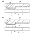
図1(A)において、第1のボンドウエハー100上に酸化シリコン膜101と窒化シリコン膜102が形成された状態を示している。第1のボンドウエハー100は結晶面が{100}の単結晶半導体基板である。第1のボンドウエハー100から単結晶半導体層を取り出すために、第1のボンドウエハー100には水素イオンを高ドーズ条件で添加する。その結果、第1のボンドウエハー100の表面が粗くなってしまう問題がある。すると、その後の張り合わせ工程で接合がうまくできないことがある。そこで第1のボンドウエハー100の表面を保護するために、酸化シリコン膜101を設けておくと好ましい。酸化シリコン膜101は熱酸化により形成することが望ましく、例えば、水蒸気雰囲気下で900〜1100℃の熱処理により形成すると良い。酸化シリコン膜101のその他の製法として、酸素プラズマ処理によりシリコンを酸化して形成しても良く、熱酸化に比べて低温で緻密な酸化シリコン膜を作製することができる。または、酸化シリコン膜101として、気相成長法で酸化シリコン膜を堆積し、その表面を酸素プラズマ処理で緻密化しても良く、熱酸化に比べて低温で作製することができる。
FIG. 1A shows a state in which a
酸化シリコン膜101の上には、窒化シリコン膜102を形成する。窒化シリコン膜102は、シランとアンモニアを用いて気相成長法により堆積させることで形成すれば良い。窒化シリコン膜102は、第1のボンドウエハー100を溝加工する際のハードマスクとして用いる。溝加工は、MISFETの半導体層の形状を考慮して行われる。すなわちMISFETの半導体層がベース基板に転置できるように、その転置する部位が凸状部として残存するように第1のボンドウエハー100に対して溝加工を行う。図1(B)で示すように、フォトレジストでマスクパターン103を形成し、窒化シリコン膜102及び酸化シリコン膜101をエッチングする。
A
次いで、図1(C)で示すように、窒化シリコン膜102をハードマスクとして第1のボンドウエハー100のエッチングを行う。第1のボンドウエハー100をエッチングする深さは、ベース基板に転置する単結晶半導体層の厚さを考慮して決定される。当該単結晶半導体層の厚さは水素イオンを添加する深さで制御することが可能である。第1のボンドウエハー100に形成する溝の深さは、脆化層よりも深くなるように形成することが好ましい。
Next, as shown in FIG. 1C, the
図1(D)において行う水素イオンの添加はベース基板に転置する単結晶半導体層の厚さを考慮して行われる。当該単結晶半導体層の厚さは10nm乃至200nm、好ましくは10nm乃至50nmの厚さとする。単結晶半導体層の厚さが薄いと、移動度の向上、S値の向上、短チャネル効果抑制を図ることができる。水素イオンを添加する際の加速電圧はこのような厚さを考慮して、第1のボンドウエハー100に添加されるようにする。この処理によって第1のボンドウエハー100の表面から一定の深さの領域に脆化層104が形成される。この脆化層104は、水素のみでなく希ガスを用いてもよく、或いは両者を混合させて用いても良い。イオン添加の工程を行った後、表面の窒化シリコン膜102を除去する。
In FIG. 1D, hydrogen ions are added in consideration of the thickness of the single crystal semiconductor layer transferred to the base substrate. The single crystal semiconductor layer has a thickness of 10 nm to 200 nm, preferably 10 nm to 50 nm. When the thickness of the single crystal semiconductor layer is small, mobility, S value, and short channel effect can be suppressed. The acceleration voltage when adding hydrogen ions is added to the
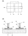
図2(A)で示すように第1のボンドウエハー100における酸化シリコン膜101の表面とベース基板105を接合させる、所謂貼り合わせ工程を行う。接合が低温で可能なため、ベース基板105は様々なものが適用可能であり、その材質としては、ガラス、石英、サファイアなどの絶縁基板、シリコン、ガリウムヒ素、インジウムリンなどの半導体基板などを適用することができる。
As shown in FIG. 2A, a so-called bonding process is performed in which the surface of the
ベース基板105の表面には、窒化シリコン膜106と酸化シリコン膜107が形成されている。窒化シリコン膜106はベース基板105からナトリウムイオンなどの不純物が拡散して単結晶半導体層を汚染しないために設けられている。この目的のためには、窒化シリコン膜に替えて、窒化酸化シリコン膜(その組成として、酸素よりも窒素の含有量が多いものであって、ラザフォード後方散乱法(RBS:Rutherford Backscattering Spectrometry)及び水素前方散乱法(HFS:Hydrogen Forward Scattering)を用いて測定した場合に、濃度範囲として酸素が5〜30原子%、窒素が20〜55原子%、Siが25〜35原子%、水素が10〜30原子%の範囲で含まれるものをいう)、窒化アルミニウム、窒素酸化アルミニウムなどを適用することができる。ベース基板105から単結晶半導体層に悪影響を与える不純物の拡散がない場合には、窒化シリコン膜106を省略することも可能である。一方、酸化シリコン膜107は、酸化シリコン膜101と接合を形成するために設けられている。この場合、酸化シリコン膜に替えて、酸化窒化シリコン膜(その組成として、窒素よりも酸素の含有量が多いものであって、RBS及びHFSを用いて測定した場合に、濃度範囲として酸素が50〜70原子%、窒素が0.5〜15原子%、Siが25〜35原子%、水素が0.1〜10原子%の範囲で含まれるものをいう)を適用することができる。
A
接合は、表面が清浄された第1のボンドウエハー100側の酸化シリコン膜101と、ベース基板側の酸化シリコン膜107が密接することにより形成される。接合の形成は室温で行うことが可能である。この接合は原子レベルで行われ、ファン・デル・ワールス力が作用して室温で強固な接合が形成される。第1のボンドウエハー100には溝加工がされているので、単結晶半導体層を形成する凸状部がベース基板105と接する。
The bonding is formed by bringing the
第1のボンドウエハー100とベース基板105との間で接合を形成した後、図2(B)で示すように第1のボンドウエハー100から単結晶半導体層を剥離してベース基板105に固定する。単結晶半導体層の剥離は、脆化層104に形成された微少な空洞の体積変化が起こり、亀裂が生じるなどし、脆化層104に沿って破断面を発生させることにより行う。破断面を発生させ、さらに接合を強固なものとするために、400℃乃至600℃の熱処理を行うことが好ましい。このようにして、絶縁表面上に単結晶半導体層(以下、「SOI層」ともいう)が形成される。図2(B)では第1のSOI層108がベース基板105上に接合された状態を示している。
After a bond is formed between the
第1のボンドウエハー100の結晶面が{100}である場合、第1のSOI層108の結晶面も{100}となる。他の結晶面のSOI層をベース基板105に形成するには、その結晶面を有するボンドウエハーを用いればよい。
When the crystal plane of the
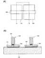
図3は、第1のボンドウエハー100とは結晶面が異なる第2のボンドウエハー109(例えば、結晶面が{110}のウエハー)から単結晶半導体層を剥離した後を示している。第2のボンドウエハー109には脆化層104が形成されており、第1のボンドウエハー100と同様にして、第2のSOI層110をベース基板105上に接合する。
FIG. 3 shows a state after the single crystal semiconductor layer is peeled from a second bond wafer 109 (for example, a wafer whose crystal plane is {110}) having a crystal plane different from that of the
以上の工程により、互いに結晶面が異なる第1のSOI層108と第2のSOI層110がベース基板105上に設けられる。上記の工程において、第1のボンドウエハー100の結晶面が{100}である場合には第1のSOI層108の結晶面も{100}となり、第2のボンドウエハー109の結晶面が{110}である場合には、第2のSOI層110の結晶面も{110}となる。転置された第1のSOI層108及び第2のSOI層110について、その表面を平坦化するために化学的機械的研磨(Chemical Mechanical Polishing:CMP)を行うことが好ましい。第1のSOI層108及び第2のSOI層110の厚さはCMPによってさらに薄膜化されても良く、好ましくは5nm乃至25nmの厚さに調製されても良い。SOI層の厚さが薄いと、移動度の向上、S値の向上、短チャネル効果抑制を図ることができる。薄膜化するにつれ、単結晶半導体膜のS値が揃うので好ましい。
Through the above steps, the
本実施の形態の構成では、n型MISFETを結晶面が{100}の第1のSOI層108で形成することができる。また、p型MISFETは結晶面が{110}の第2のSOI層110で形成することができる。すなわち、それぞれのMISFETについて電子、ホールの電界効果移動度が最も高くなる結晶面である層にチャネル形成領域を設けることが可能となる。
In the configuration of the present embodiment, the n-type MISFET can be formed using the
本実施の形態では、水素イオンなどを一定の深さに添加して単結晶半導体層をボンドウエハーから剥離する方法について示すが、他のSOI技術を用いることも可能である。例えば、ボンドウエハーの表面を陽極化成することにより多孔質シリコン層を形成し、その上にエピタキシャル成長で形成した単結晶シリコン層を、本実施の形態で示すSOI層として用いることができる。この構成のボンドウエハーを用いる場合には、ウオータージェット法を用い、多孔質シリコン層とエピタキシャル成長した単結晶シリコン層を分離する。それにより、図2(B)又は図3に示すようなSOI層が設けられたベース基板を得ることができる。 Although this embodiment mode describes a method for adding a hydrogen ion or the like to a certain depth to separate a single crystal semiconductor layer from a bond wafer, other SOI techniques can also be used. For example, a porous silicon layer is formed by anodizing the surface of a bond wafer, and a single crystal silicon layer formed by epitaxial growth on the porous silicon layer can be used as the SOI layer described in this embodiment. When a bond wafer having this structure is used, a water jet method is used to separate the porous silicon layer from the epitaxially grown single crystal silicon layer. Thus, a base substrate provided with an SOI layer as shown in FIG. 2B or FIG. 3 can be obtained.
本実施の形態によれば、半導体装置を形成するベース基板に異なる結晶面の単結晶半導体層(SOI層)を形成することができる。当該結晶面はn型MISFET及びp型MISFETのそれぞれに対して、高い電界効果移動度が得られるように決定することが可能である。キャリアにとって移動度が高くなる結晶面及び/又は結晶軸を適用することにより、キャリアの有効質量を最も軽くすることができ、それによってキャリアの実効移動度を最も大きくすることができる。このような単結晶半導体層が設けられたベース基板を用いることにより半導体装置の高性能化を図ることができる。 According to this embodiment, single crystal semiconductor layers (SOI layers) having different crystal planes can be formed over a base substrate over which a semiconductor device is formed. The crystal plane can be determined so as to obtain high field effect mobility for each of the n-type MISFET and the p-type MISFET. By applying crystal planes and / or crystal axes that increase the mobility for the carrier, the effective mass of the carrier can be minimized, and thereby the effective mobility of the carrier can be maximized. By using a base substrate provided with such a single crystal semiconductor layer, high performance of the semiconductor device can be achieved.
(第2の実施の形態)
本実施の形態は、図1とは異なるボンドウエハーの製造工程について図4を参照して説明する。図4(A)において、第1のボンドウエハー100の表面に酸化シリコン膜101、窒化シリコン膜102を形成する。その後、水素又は希ガス、或いは水素と希ガスのイオンを添加し、第1のボンドウエハー100に脆化層104を形成する。そして、図4(B)で示すように溝加工を行う。この溝加工において、溝の深さを脆化層104よりも深く加工することで、脆化層104を剥離すべき単結晶半導体層の領域のみに残すことができる。このような構成により、より容易に転置を行うことができる。
(Second Embodiment)
In the present embodiment, a manufacturing process of a bond wafer different from that in FIG. 1 will be described with reference to FIG. In FIG. 4A, a
(第3の実施の形態)
本実施の形態は、n型MISFETとp型MISFETを構成するSOI層を、結晶面が異なる各ボンドウエハーから、ボンドウエハーとは異種であって透光性を有する絶縁基板でなるベース基板の同一表面へ転置する半導体素子基板の作製方法について説明する。本実施の形態では、n型MISFETは、結晶面{100}のボンドウエハーを用いて、チャネル形成領域、ソース領域及びドレイン領域を形成する。またp型MISFETは、結晶面{110}のボンドウエハーを用いて、チャネル形成領域、ソース領域及びドレイン領域を形成する。また本実施の形態ではn型MISFETのSOI層を、透光性を有する絶縁基板へ転置後に、p型のMISFETのSOI層を該絶縁基板へ転置する順序で説明するが、どちらを先に転置しても構わない。
(Third embodiment)
In this embodiment, the SOI layers constituting the n-type MISFET and the p-type MISFET are made of the same base substrate made of an insulating substrate that is different from the bond wafer and has translucency from each bond wafer having a different crystal plane. A method for manufacturing a semiconductor element substrate to be transferred to the surface will be described. In the present embodiment, the n-type MISFET forms a channel formation region, a source region, and a drain region using a bond wafer having a crystal plane {100}. In the p-type MISFET, a channel formation region, a source region, and a drain region are formed using a bond wafer having a crystal plane {110}. In this embodiment, the n-type MISFET SOI layer is transferred to an insulating substrate having translucency, and then the p-type MISFET SOI layer is transferred to the insulating substrate. It doesn't matter.
図20(A)に示すように、結晶面を{100}とする第1のボンドウエハー100に対し、水素、又はハロゲンから選ばれたイオン種、これらが混合されたイオン種、若しくは水素又はハロゲンに希ガスが混合されたイオン種111を、所定の深さの領域に添加し、脆化層104を形成する。このとき、イオン注入法を用いると、水素又はハロゲンは、質量分離された状態で注入される。第1のボンドウエハー100には水素又はハロゲンから選ばれたイオン種を高ドーズ条件(1×10¹⁵/cm2〜1×1017/cm2)で添加するとよい。おって剥離する際、第1のボンドウエハー100からMISFETのSOI層が取り出しやすくなるからである。なお脆化層が形成される所定の深さは、おって、絶縁基板に転置された際のn型MISFETのSOI層の膜厚となる。そのため、イオン種の添加条件によって、転置された際のSOI層の膜厚を決めることができる。上記イオン種の添加に際し、直接ボンドウエハー100に添加する工程と、ボンドウエハー上に絶縁層等を形成した状態で添加する工程とのいずれも用いることができる。いずれの工程においても、添加条件によって、転写後のSOI層の膜厚と同じ深さとなるように脆化層を形成することができる。
As shown in FIG. 20A, for a
図20(B)に示すように、第1のボンドウエハー100上に、接着層112を形成する。接着層112は、酸化シリコン膜が10nm〜200nmの膜厚で、最上層に設けられている。酸化シリコン膜は、有機シランガスを用いた化学気相成長法により形成する。有機シランガスを用いた化学気相成長法により形成された酸化シリコン膜は平坦性が高く、貼り合わせ工程の際の接合を確実に行うことができる。なお、酸化シリコン膜は、熱酸化法、又はプラズマCVD法によって形成することもでき、さらにいずれの方法で形成された酸化シリコン膜に対しても、プラズマ処理を行うことができ、プラズマ処理によって酸化シリコン膜の緻密性を高めることができる。このような接着層112は、第1のボンドウエハー100の上面のみではなく、側面に形成しても、裏面に形成してもよい。
As shown in FIG. 20B, an
接着層112の最上層は酸化シリコン膜がよいが、上記酸化シリコン膜に加えてその他の膜を有してもよく、ボンドウエハーと酸化シリコン膜との間に、例えば、酸化シリコン膜、窒化シリコン膜、酸化窒化シリコン膜を有してもよい。例えば、酸化窒化シリコン膜を有する場合、窒素と酸素の濃度を異ならせた酸化窒化シリコン膜同士を積層させてもよい。酸素濃度を高めた酸化窒化シリコン(SiON)膜は、最上層に形成される酸化シリコン膜と、他の層との接着性を高める機能を有し、窒素濃度を高めた窒化酸化シリコン(SiNO)膜は、不純物汚染を防ぐ機能を有する。そのため、第1のボンドウエハー上に、SiNO膜、SiON膜、酸化シリコン膜の順に積層された接着層112を形成するとよい。
The uppermost layer of the
なお、接着層112の最上層に設けられた酸化シリコン膜は、高ドーズ条件での添加の結果、表面が荒れてしまう第1のボンドウエハー100の平坦性を維持させる機能も有する。
Note that the silicon oxide film provided on the uppermost layer of the
図20(C)に示すように、第1ボンドウエハー100上に、レジスト等のマスク113を選択的に設ける。該マスクは、おって転置されるp型のMISFETのSOI層の配置を考慮して選択的に設ける。n型のMISFETのSOI層と、p型のMISFETのSOI層とが、隣接するように配置されると、CMOS回路の作製を簡便なものとすることができる。
As shown in FIG. 20C, a
図20(D)に示すように、マスク113を用いて、第1のボンドウエハー100と接着層112とに対してエッチングを行って、n型のMISFETのSOI層108を形成する。SOI層108は、その上には接着層が残存した状態であって、矩形状となっている。なお、マスク113を用いて接着層112を先にエッチングし、接着層112をマスクとして第1のボンドウエハー100をエッチングしてもよい。いずれの方法によるエッチングに対しても、第1のボンドウエハー100に対して、少なくとも脆化層104が露出するまでエッチングを行うとよい。おってSOI層108の転置が行われる際、脆化層を境界にして第1のボンドウエハー100が剥がれるためである。
As shown in FIG. 20D, the
次に、透光性を有する絶縁基板(ベース基板となる)105を用意する。絶縁基板105には、ガラス、石英、プラスチック、サファイアなどを用いることができ、半導体表示装置に好適である。また透光性が必要とされない装置を作製するのであれば、絶縁基板105として、シリコン、ガリウムヒ素、インジウムリンなどの半導体基板を用いることができる。絶縁基板105上に、シリコンを有する膜を形成してもよい。シリコンを有する膜として、酸化シリコン膜、窒化シリコン膜、酸化窒化シリコン膜がある。酸化シリコン膜は、有機シランガスを用いた化学気相成長法により形成することができる。有機シランガスを用いた化学気相成長法により形成された酸化シリコン膜は、絶縁基板105の平坦性を高めることができ、接着層112との接着性を高めることができる。不純物汚染を防ぐ機能を高めるため、窒素濃度を高めた窒化酸化シリコン(SiNO)膜としてもよく、その他の不純物汚染防止機能の高い窒化アルミニウム、又は窒素酸化アルミニウムを採用してもよい。酸化窒化シリコン膜の他の層との接着性を高めるため、酸素濃度を高めた酸化窒化シリコン(SiON)膜としてもよい。このようなシリコンを有する膜は、化学気相成長法以外に熱酸化法、又はプラズマCVD法によって形成することもできる。
Next, a light-transmitting insulating substrate 105 (to be a base substrate) is prepared. Glass, quartz, plastic, sapphire, or the like can be used for the insulating
そして図21(A)に示すように、選択的にエッチングされた接着層を介して、透光性を有する絶縁基板105と、第1のボンドウエハー100とを重ね合わせる。このとき、重ね合わせられる互いの面に対して、それぞれ洗浄を行うとよい。選択的にエッチングされた接着層の最上層には、酸化シリコン膜が設けられており、該酸化シリコン膜によって絶縁基板105との接着性が高まる。このとき絶縁基板105上にも酸化シリコン膜が形成されていると、より接着性を高めることができる。絶縁基板105、又は絶縁基板上の酸化シリコン膜と第1のボンドウエハー100との接合の形成は室温で行うことが可能である。この接合は原子レベルで行われ、ファン・デル・ワールス力が作用して室温で強固な接合が形成される。接着性を高めるため、絶縁基板105と、第1のボンドウエハー100とを重ね合わせた状態で、加熱処理を行ってもよい。加熱処理を行うと、接着性の向上に加えて、脆化層104に亀裂を生じさせることができるため、MISFETのSOI層の取り出し、つまり第1のボンドウエハー100の剥離を簡便なものとすることができる。該亀裂は、脆化層104に形成された微小な空洞の体積変化によって起こり得る。接合を強固なものにしつつ、脆化層104に沿って破断面を発生させるために、加熱処理は400℃乃至600℃で、5分から30分程度、例えば600℃で20分間行うとよい。また加熱処理に加えて加圧処理を行ってもよく、両処理を同時に行ってもよい。
Then, as shown in FIG. 21A, the light-transmitting
図21(B)に示すように、絶縁基板105上にSOI層108を残存させたまま、脆化層104を境界として、第1のボンドウエハー100を剥離することができる。第1のボンドウエハー100の結晶面が{100}であれば、SOI層108の結晶面も{100}となっており、移動度の高いn型のMISFETを提供することができる。
As shown in FIG. 21B, the
次に図22(A)に示すように、結晶面を{110}とする第2のボンドウエハー109に対し、図1及び図2で示した工程と同様にして、SOI層110を形成する。同様な工程ではあるが、適宜再掲して説明する。まず水素又はハロゲンから選ばれたイオン種をイオン注入法又はイオンドーピング法により添加して脆化層を形成し、接着層112を形成する。接着層112の最上層は、酸化シリコン膜を有するため、絶縁基板105との接着性を高めることができる。酸化シリコン膜は、有機シランガスを用いた化学気相成長法等により形成するとよいことも図1及び図2と同様である。また絶縁基板105上にもシリコンを有する膜を形成することによって、第2のボンドウエハー109との接着性を高めることができることも図1及び図2と同様である。絶縁基板105と、第2のボンドウエハー109とを重ね合わせた状態で、加熱処理を行って、接着性を高めてもよいことも図1及び図2と同様である。加熱処理を行うと、脆化層104に亀裂を生じさせることができ、また加熱処理に加えて加圧処理を行ってもよく、両処理を同時に行ってもよいことも図1及び図2と同様である。また脆化層104は、SOI層110が設けられていない領域では露出するようにエッチングされることも図1及び図2と同様である。そして、凸部状のSOI層110を選択的に形成し、酸化シリコン膜がSOI層110の上面に設けられていることも図1及び図2と同様である。
Next, as shown in FIG. 22A, an
図22(B)に示すように、SOI層108が転置された絶縁基板105と、SOI層110が選択的に形成された第2のボンドウエハー109とを重ね合わせる。SOI層110は、図20(D)及び図21で示したSOI層108と隣接するように重ね合わせると、CMOS回路の作製を簡便なものとすることができる。
As shown in FIG. 22B, the insulating
重ね合わせる際、SOI層108をSOI層110より薄くしておくと、不必要な領域での接着を防止することができる。すなわち、SOI層108とSOI層110とが同じ膜厚の場合と比較すると、SOI層108と、第2のボンドウエハー109との接着を積極的に防ぐことができる。このようにSOI層108を、SOI層110より薄くするためには、第1のボンドウエハー100における脆化層104と、第2のボンドウエハー109における脆化層104との深さを異ならせればよい。すなわち、各脆化層104を形成する際のドーズ量等を異ならせればよい。またボンドウエハーの結晶面が異なっているため、ドーズ量を等しくした状態でもボンドウエハー毎にイオン種の添加深さが変わることもある。これを利用して各脆化層の深さを異ならせることもできる。
If the
その後図22(C)に示すように、第2のボンドウエハー109と、絶縁基板105との剥離を行う。すると、SOI層108が転置された絶縁基板105上に、SOI層110を残存させたまま、脆化層104を境界として、第2のボンドウエハー109を剥離することができる。このとき、上記加熱処理により脆化層104に亀裂が生じていると、該剥離を簡便に行うことができる。
After that, as shown in FIG. 22C, the
絶縁基板105上に転置されたSOI層108と、SOI層110とに対して平坦化処理を行ってもよい。平坦化処理にはレーザ照射、加熱処理、又はCMP研磨のいずれか若しくはこれらを複数組み合わせた方法を用いることができる。またSOI層108と、SOI層110との表面の高さが異なっている場合、異なった状態、つまりSOI層108の膜厚が、SOI層110の膜厚より薄いままでもよいし、高さを揃えてもよい。高さを揃えるためにはSOI層110のみを薄くすればよいため、CMP研磨を用いるとよい。このとき両SOI層をさらに薄膜化してもよく、好ましくは5nm乃至25nmの厚さとなるように研磨してもよい。SOI層が薄膜化されると、移動度の向上、S値の向上、短チャネル効果抑制が向上される。薄膜化するにつれ、単結晶半導体膜のS値が揃うので好ましい。
Planarization treatment may be performed on the
このように絶縁基板の同一表面に、結晶面が異なるn型のMISFETのSOI層と、p型のMISFETのSOI層とを転置することによって、上記移動度等が高められた半導体素子及び半導体集積回路を提供することができる。さらに、透光性も確保されているため、該半導体集積回路等を半導体表示装置に用いると好適である。本発明の半導体表示装置は、透光性を有する絶縁基板上に、移動度をはじめとする電気特性の高いMISFETを転置したため動作の高速化を図ることができ、また低電圧で駆動することが可能となり、低消費電力化を図ることができる。また、本実施の形態によれば素子分離を行うための構造を形成する必要がないので製造工程を簡略化できる。 As described above, by transferring the n-type MISFET SOI layer and the p-type MISFET SOI layer having different crystal planes on the same surface of the insulating substrate, the above-described mobility and the like are improved. A circuit can be provided. Further, since the light-transmitting property is also ensured, the semiconductor integrated circuit or the like is preferably used for a semiconductor display device. In the semiconductor display device of the present invention, a MISFET with high electrical characteristics such as mobility is transferred over a light-transmitting insulating substrate, so that the operation speed can be increased, and the semiconductor display device can be driven at a low voltage. It becomes possible, and low power consumption can be achieved. Further, according to the present embodiment, it is not necessary to form a structure for element isolation, so that the manufacturing process can be simplified.
また本実施の形態では、水素イオンなどを一定の深さに添加して、SOI層となる単結晶半導体層をボンドウエハーからベース基板へ転置する方法について示したが、他のSOI技術を用いて同様なベース基板を作製することも可能である。例えば、ボンドウエハーの表面を陽極化成することにより多孔質シリコン層を形成し、その上にエピタキシャル成長で形成した単結晶シリコン層を、本実施の形態で示すSOI層として用いることができる。この構成のボンドウエハーを用いる場合には、ウオータージェット法を用い、多孔質シリコン層とエピタキシャル成長した単結晶シリコン層を分離することもできる。 In this embodiment mode, a method is described in which a single crystal semiconductor layer to be an SOI layer is transferred from a bond wafer to a base substrate by adding hydrogen ions or the like to a certain depth, but other SOI technologies are used. A similar base substrate can be manufactured. For example, a porous silicon layer is formed by anodizing the surface of a bond wafer, and a single crystal silicon layer formed by epitaxial growth on the porous silicon layer can be used as the SOI layer described in this embodiment. In the case of using a bond wafer having this configuration, the water jet method can be used to separate the porous silicon layer and the epitaxially grown single crystal silicon layer.
(第4の実施の形態)
本実施の形態では、図23(A)に示すように、最初に、結晶面を{100}とする第1のボンドウエハーを選択的にエッチングし、その後図23(B)に示すように脆化層を形成し、結晶面が異なるn型のMISFETのSOI層と、p型のMISFETのSOI層とを、同一絶縁基板上に転置する作製工程を説明する。
(Fourth embodiment)
In this embodiment mode, as shown in FIG. 23A, first, a first bond wafer having a crystal plane of {100} is selectively etched, and then, as shown in FIG. A manufacturing process in which an n-type MISFET SOI layer and a p-type MISFET SOI layer having different crystal planes and a p-type MISFET are transferred on the same insulating substrate will be described.
図23(A)に示すように、第1のボンドウエハー100上に選択的にレジスト等のマスク113を形成する。マスク113は上記実施の形態で示したように、CMOS回路の作製を簡便なものとするため、おって転置されるp型のMISFETのSOI層の配置を考慮して選択的に設ける。
As shown in FIG. 23A, a
図23(B)に示すように、マスク113を用いて、n型のMISFETのSOI層108を形成する。すなわち、第1のボンドウエハー100にSOI層108となる凸部が形成される。その後、上記実施の形態と同様なイオン種111を、第1のボンドウエハー100に添加して脆化層104を形成する。脆化層104は、第1のボンドウエハー100の表面から所定の深さに形成されるため、SOI層108となる領域での脆化層は、その他の領域の脆化層よりも、第1のボンドウエハー100の表面側に形成される。
As shown in FIG. 23B, an n-type
図23(C)に示すように、上記実施の形態と同様な接着層112を形成する。接着層112は、第1のボンドウエハー100の表面を沿うように形成される。つまりSOI層108を覆うように形成される。
As shown in FIG. 23C, an
図23(D)に示すように、上記実施の形態と同様な絶縁基板105を、接着層112を介して第1のボンドウエハー100に重ね合わせる。接着層112の最上層には、酸化シリコン膜が設けられており、該酸化シリコン膜によって絶縁基板105との接着性が高まること、絶縁基板105上に酸化シリコン膜が形成されていることでより接着性が高まることは、上記実施の形態と同様である。なお本実施の形態において、第1のボンドウエハー100は、SOI層108の凸部で絶縁基板105と積極的に接着する。絶縁基板105と、第1のボンドウエハー100とを重ね合わせた状態で、加熱処理を行って、接着性を高めてもよく、加熱処理を行うと、接着性の向上に加えて、脆化層104に亀裂を生じさせることができることは、上記実施の形態と同様である。また加熱処理に加えて加圧処理を行ってもよく、両処理を同時に行ってもよいことも、上記実施の形態と同様である。
As shown in FIG. 23D, an insulating
その後、上記実施の形態と同様に、第1のボンドウエハー100と、絶縁基板105との剥離を行って、SOI層108が転置された絶縁基板105を形成する。そして、該絶縁基板上に、p型のMISFETのSOI層を転置する。該SOI層は、本実施の形態と同様な工程に基づき、第2のボンドウエハーを選択的にエッチングし、その後、脆化層を形成して得られた、p型のMISFETのSOI層である。該SOI層を、SOI層108が転置された絶縁基板105に転置する。
After that, as in the above embodiment, the
このように少なくとも結晶面が異なるn型のMISFETのSOI層と、p型のMISFETのSOI層とを、絶縁基板の同一表面に転置することによって、移動度が高められた半導体集積回路等を提供することができ、透光性も確保されているため、該半導体集積回路を半導体表示装置に用いることができる。本発明の半導体表示装置は、透光性を有する絶縁基板上に、移動度が高いMISFETを転置したため動作の高速化を図ることができ、また低電圧で駆動することが可能となり、低消費電力化を図ることができる。また、本実施の形態によれば素子分離を行うための構造を形成する必要がないので製造工程を簡略化できる。 As described above, a semiconductor integrated circuit or the like having improved mobility is provided by transferring at least the n-type MISFET SOI layer and the p-type MISFET SOI layer having different crystal planes on the same surface of the insulating substrate. In addition, since the light-transmitting property is ensured, the semiconductor integrated circuit can be used for a semiconductor display device. In the semiconductor display device of the present invention, a high-mobility MISFET is transferred over a light-transmitting insulating substrate, so that the operation speed can be increased, and the semiconductor display device can be driven at a low voltage. Can be achieved. Further, according to the present embodiment, it is not necessary to form a structure for element isolation, so that the manufacturing process can be simplified.
なお本実施の形態においても、n型MISFETのSOI層を、透光性を有する絶縁基板へ転置後に、p型のMISFETのSOI層を該絶縁基板へ転置する順序で説明したが、どちらを先に転置しても構わない。 In this embodiment, the n-type MISFET SOI layer is transferred to an insulating substrate having translucency, and then the p-type MISFET SOI layer is transferred to the insulating substrate. May be transposed.
また本実施の形態では、水素イオンなどを一定の深さに添加して単結晶半導体層をボンドウエハーから剥離する方法について示したが、他のSOI技術を用いて同様なベース基板を作製することも可能である。例えば、ボンドウエハーの表面を陽極化成により多孔質シリコン層を形成し、その上にエピタキシャル成長で形成した単結晶シリコン層を、本実施の形態で示すSOI層として用いることができる。この構成のボンドウエハーを用いる場合には、ウオータージェット法を用い、多孔質シリコン層とエピタキシャル成長した単結晶シリコン層を分離することもできる。 In this embodiment mode, a method for removing a single crystal semiconductor layer from a bond wafer by adding hydrogen ions or the like to a certain depth is described; however, a similar base substrate is manufactured using another SOI technology. Is also possible. For example, a single crystal silicon layer formed by epitaxially growing a porous silicon layer on the surface of a bond wafer by anodization can be used as the SOI layer described in this embodiment. In the case of using a bond wafer having this configuration, the water jet method can be used to separate the porous silicon layer and the epitaxially grown single crystal silicon layer.
(第5の実施の形態)
本実施の形態では、図24と図26で示すように、ボンドウエハーの周囲を酸化膜で覆った状態を経た作製工程を説明する。本実施の形態は、酸化膜で覆う以外の工程、例えば上記実施の形態のようにボンドウエハーに脆化層を形成した後に選択的にエッチングする工程や上記実施の形態のようにボンドウエハーを選択的にエッチングした後脆化層を形成する工程と、自由に組み合わせることができる。
(Fifth embodiment)
In this embodiment mode, as shown in FIGS. 24 and 26, a manufacturing process through a state in which the periphery of a bond wafer is covered with an oxide film will be described. In this embodiment, a process other than covering with an oxide film, for example, a step of selectively etching after forming an embrittlement layer on the bond wafer as in the above embodiment, or a bond wafer as in the above embodiment is selected. It can be freely combined with the step of forming the embrittlement layer after etching.
図24(A)において、結晶面を{100}とする第1のボンドウエハー100を、硫酸過水(SPM)、アンモニア過水(APM)、塩酸過水(HPM)、希フッ酸(DHF)などにより洗浄する。その後、第1のボンドウエハー100の熱酸化を行う。熱酸化はドライ酸化で形成することができるし、酸化雰囲気中にハロゲンを添加した酸化を行って形成することもできる。ハロゲンを含むものとしては塩素を含むHClが代表例であり、その他にもHF、NF3、HBr、Cl2、ClF3、BCl3、F2、Br2などから選ばれた一種又は複数種を適用することができる。このような熱酸化の例としては、酸素に対しHClを0.5〜10体積%(好ましくは3体積%)の割合で含む雰囲気中で、900℃〜1150℃の温度(代表的には1000℃)で熱酸化を行うとよい。
このような温度範囲で熱処理を行うことで、第1のボンドウエハー100内の不純物元素に対するハロゲン元素によるゲッタリング効果を得ることができる。ゲッタリング効果としては、特に金属不純物(外因性不純物である重金属)を除去する効果が得られる。代表的な重金属としてはFe、Cr、Niといった金属であり、さらにMoが含まれる場合もある。その際、塩素等のハロゲンの作用により、第1のボンドウエハー100内の金属などの不純物が揮発性の塩化物となって気相中へ離脱して除去される。第1のボンドウエハー100の表面を化学的機械研磨(CMP)処理したものに対しては、不純物を効率的に除去することができる。このように酸化膜120にハロゲンが含まれることにより、外因性不純物である重金属を捕集して第1のボンドウエハー100が汚染されることを防止する効果を奏することができる。また、HClの水素は第1のボンドウエハー100と酸化膜120の界面の欠陥を補償して界面の局在準位密度を低減する作用を奏する。熱酸化の処理時間は0.1〜6時間、好ましくは0.5〜1時間とすれば良い。このようにして形成される酸化膜は、10nm〜1000nm(好ましくは50nm〜200nm)、例えば100nmの厚さとする。
In FIG. 24A, a
By performing the heat treatment in such a temperature range, the gettering effect by the halogen element with respect to the impurity element in the
図24(B)は上記実施の形態と同様な水素又はハロゲン等のイオン種を添加して脆化層104を形成する工程を示している。イオン種の添加は、第1のボンドウエハー100に対して斜め方向から行うこともできる。なお、重金属は第1のボンドウエハー100に対し、質量分離されないイオンをドーピングして脆化層104を形成する過程で導入される。
FIG. 24B shows a step of forming the
図25は第1のボンドウエハー100に添加した水素又はハロゲンイオンの分布を曲線Hとして示す。第1のボンドウエハー100に添加された水素又はハロゲンイオンはガウス分布する。勿論、イオンを電界で加速してボンドウエハーに添加する場合には、イオンはある深さをピークにしてほぼガウス分布することとなり、ここでそのピーク位置を目安として脆化層104を示している。第1のボンドウエハー100の表面からイオンの平均進入深さに近い深さ領域に脆化層104が形成される。例えば、脆化層104は、SOI層の厚さ5nm〜500nm、好ましくは10nm〜200nmに合わせた深さに形成することが好ましく、イオンを添加する際の加速電圧やドーズ量はこのような厚さを考慮して行う。
FIG. 25 shows the distribution of hydrogen or halogen ions added to the
なお、重金属のイオンは質量数が大きいので、第1のボンドウエハーのうちイオンが添加される側のごく表面に多く分布する。第1のボンドウエハー100の表面に酸化膜120が形成されているため、この酸化膜120の膜厚を金属イオンの添加深さよりも厚く形成することで、当該金属の分布を酸化膜120中に止めておくことができる(図25において示す曲線M)。膜中にハロゲンを含んだ酸化膜120はHCl酸化などによって、酸化膜120中に捕集した当該重金属を固定して第1のボンドウエハー100の汚染を防ぐことができる。
Since the heavy metal ions have a large mass number, they are distributed in a large amount on the very surface of the first bond wafer on the side where ions are added. Since the
さらに酸化膜120を形成した後に行われる熱処理により、第1のボンドウエハー100に含まれる不純物としての他の金属が酸化膜120に析出し、ハロゲン(例えば塩素)と反応して捕獲される。それにより酸化膜120中に捕集した当該不純物を固定して第1のボンドウエハー100の汚染を防ぐことができる。
Further, another metal as an impurity contained in the
このように本実施の形態の酸化膜120は、重金属や不純物を捕獲して再拡散させないことにより、MISFETの高性能化を図ることができる。
As described above, the
なお、脆化層104は、イオン種を質量分離した上で、第1のボンドウエハー100に添加しても同様に形成することができる。この場合にも、質量の大きいイオン(例えばH3 +イオン)を選択的に添加することは上記ゲッタリング効果と同様な効果を奏することができる。
Note that the
そして図24(C)に示すように、上記実施の形態と同様に接着層112を形成し、マスク113を用いて、脆化層104より上の、第1のボンドウエハー100及び接着層112をエッチングする。その後の工程は、上記実施の形態と同様に行うことができるため、説明を省略する。
Then, as shown in FIG. 24C, an
これまでは、ボンドウエハーに脆化層を形成した後に選択的にエッチングする工程を用いて説明したが、ボンドウエハーを選択的にエッチングした後脆化層を形成する工程を用いることもできる。図26(A)に示すように、第1のボンドウエハー100を、マスク113を用いてエッチングする。その後図26(B)に示すように、エッチングされた第1のボンドウエハー100に対して、酸化膜120を形成する。酸化膜120の形成は、上述したとおりである。図26(C)に示すように、脆化層104を形成し、図26(D)に示すように接着層112を形成する。その後の工程は、上記実施の形態と同様に行うことができるため、説明を省略する。
Up to now, the step of selectively etching after forming the embrittlement layer on the bond wafer has been described. However, the step of forming the embrittlement layer after selectively etching the bond wafer can also be used. As shown in FIG. 26A, the
このようにして、ボンドウエハーに対して酸化膜を形成してもよい。その結果、脆化層の形成の際にボンドウエハーに含まれてしまう重金属や不純物等をゲッタリングすることができ、ボンドウエハーの汚染を低減することができる。 In this way, an oxide film may be formed on the bond wafer. As a result, heavy metals, impurities, and the like that are contained in the bond wafer when the embrittlement layer is formed can be gettered, and contamination of the bond wafer can be reduced.
(第6の実施の形態)
結晶面の異なるSOI層をベース基板に接合する場合に、より好ましい態様として、チャネル長方向の結晶軸を特定の方向とする。SOI層の結晶面での結晶軸の異方性と、SOI層のキャリアの流れる方向での結晶軸の異方性とを合わせることで、MISFETのチャネル形成領域を流れる電子又はホールのキャリア移動度を高めることができる。この原因として、結晶中でキャリアの有効質量が異方性を有するからである。
(Sixth embodiment)
When bonding SOI layers having different crystal planes to the base substrate, as a more preferable aspect, the crystal axis in the channel length direction is set to a specific direction. By combining the anisotropy of the crystal axis in the crystal plane of the SOI layer with the anisotropy of the crystal axis in the direction of carrier flow in the SOI layer, the carrier mobility of electrons or holes flowing in the channel formation region of the MISFET Can be increased. This is because the effective mass of carriers in the crystal has anisotropy.
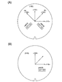
図5(A)で示すように、結晶面{100}のボンドウエハーからn型MISFET用のSOI層を取り出す場合には、SOI層のチャネル長方向が<100>方位と平行な方向になるようにすることが好ましい。なお、<100>方位と平行な方向は、(a)で示す方向に加えて、(b)で示す方向もあるため、いずれの方向と平行となるようにSOI層を取り出してもよい。 As shown in FIG. 5A, when an SOI layer for an n-type MISFET is taken out from a bond wafer having a crystal plane {100}, the channel length direction of the SOI layer is parallel to the <100> orientation. It is preferable to make it. Since the direction parallel to the <100> orientation includes the direction shown in (b) in addition to the direction shown in (a), the SOI layer may be taken out so as to be parallel to any direction.
一方、p型MISFET用のSOI層を形成するには、図5(B)で示すように結晶面{110}のボンドウエハーを用い、SOI層のチャネル長方向が<110>方位と平行な方向になるようにすることが好ましい。このように、n型MISFETについて<100>方位、p型MISFETについて<110>方位とすれば、チャネル形成領域を流れる電子とホールの移動度をより高めることができる。 On the other hand, in order to form the SOI layer for the p-type MISFET, a bond wafer having a crystal plane {110} is used as shown in FIG. 5B, and the channel length direction of the SOI layer is parallel to the <110> orientation. It is preferable that Thus, when the <100> orientation is used for the n-type MISFET and the <110> orientation is used for the p-type MISFET, the mobility of electrons and holes flowing in the channel formation region can be further increased.
(第7の実施の形態)
本実施の形態は、同一の結晶面を有するボンドウエハーから、n型MISFETとp型MISFETに適したSOI層を取り出す構成について示す。図6は結晶面{110}のボンドウエハーを用いる場合について示す。この場合、n型MISFET用のSOI層を取り出す場合には、チャネル長方向が<100>方位と平行な方向になるようにする。一方、p型MISFET用のSOI層を形成するには、チャネル長方向が<110>方位と平行な方向になるようにする。
(Seventh embodiment)
In this embodiment mode, a structure in which an SOI layer suitable for an n-type MISFET and a p-type MISFET is extracted from a bond wafer having the same crystal plane is described. FIG. 6 shows the case where a bond wafer having a crystal plane {110} is used. In this case, when the SOI layer for the n-type MISFET is taken out, the channel length direction is set to be parallel to the <100> direction. On the other hand, in order to form the SOI layer for the p-type MISFET, the channel length direction is set to be parallel to the <110> direction.
本実施の形態によれば、絶縁基板上に、n型MISFETが形成される第1のSOI層とp型MISFETが形成される第2のSOI層とが同じ結晶面であって、チャネル長方向の結晶軸の向きが互いに異なる半導体集積回路を得ることができる。n型MISFETについて<100>方位、p型MISFETについて<110>方位を選択すればチャネル形成領域を流れる電子とホールの電界効果移動度をより高めることが可能となる。また、n型MISFETのSOI層とp型MISFETのSOI層とは個別にベース基板に接合可能である。そのため同じ結晶面を有する基板から結晶軸の向きが互いに異なるようにレイアウトする場合と比較して、n型MISFETとp型MISFETの回路配置に設計の自由度が確保されるので、半導体集積回路の集積度を向上させることができる。n型MISFET及びp型MISFETのそれぞれに対して、高い電界効果移動度が得られる結晶面若しくは結晶軸を選択することが可能であるので、このようなベース基板を用いることにより半導体集積回路の高性能化を図ることができる。 According to the present embodiment, on the insulating substrate, the first SOI layer in which the n-type MISFET is formed and the second SOI layer in which the p-type MISFET are formed have the same crystal plane, and the channel length direction Semiconductor integrated circuits having different crystal axis directions can be obtained. If the <100> orientation is selected for the n-type MISFET and the <110> orientation is selected for the p-type MISFET, the field effect mobility of electrons and holes flowing in the channel formation region can be further increased. The SOI layer of the n-type MISFET and the SOI layer of the p-type MISFET can be individually bonded to the base substrate. Therefore, as compared with the case where the crystal axes are arranged in different directions from the substrate having the same crystal plane, the design freedom is ensured in the circuit arrangement of the n-type MISFET and the p-type MISFET. The degree of integration can be improved. For each of the n-type MISFET and the p-type MISFET, it is possible to select a crystal plane or a crystal axis that can provide a high field effect mobility. Performance can be improved.
また本発明の半導体集積回路を透光性を有する絶縁基板上に転置した半導体表示装置は、移動度が高いMISFETを転置したため動作の高速化を図ることができ、また低電圧で駆動することが可能となり、低消費電力化を図ることができる。 In addition, a semiconductor display device in which the semiconductor integrated circuit of the present invention is transferred over a light-transmitting insulating substrate can operate at a high speed because the MISFET having high mobility is transferred, and can be driven at a low voltage. It becomes possible, and low power consumption can be achieved.
(第8の実施の形態)
本実施の形態は、本発明のベース基板を用いてインバータ回路を作製する工程について説明する。なお、本発明はこのような単純な回路に限定されず、マイクロプロセッサをはじめとする様々な半導体装置を実現することができる。図7乃至図13において(A)はインバータ回路の平面図を示し、(B)はA−B線に対応する断面図を示す。
(Eighth embodiment)
In this embodiment mode, a process for manufacturing an inverter circuit using the base substrate of the present invention will be described. Note that the present invention is not limited to such a simple circuit, and various semiconductor devices including a microprocessor can be realized. 7A to 13A are plan views of the inverter circuit, and FIG. 7B is a cross-sectional view corresponding to the line AB.
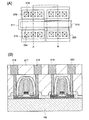
図7(A)(B)は第1のSOI層201及び第2のSOI層202が設けられたベース基板105にゲート絶縁層及びゲート電極を形成する工程を示している。第1のSOI層201及び第2のSOI層202上には、ゲート電極204が設けられる。ゲート絶縁層203としては、酸化シリコン(SiOx)、酸化窒化シリコン(SiOxNy)、酸化ハフニウム(HfOx)、酸化アルミニウム(AlxOy、x>y>0)、酸化タンタル(TaxOy、x>y>0)などの材料を適用することができる。図7(B)では、ゲート絶縁層203とゲート電極204の側端部が揃うように加工されているが、ゲート電極204のエッチングにおいてゲート絶縁層203を残すように加工しても良い。
7A and 7B illustrate a step of forming a gate insulating layer and a gate electrode over the
なお、本実施の形態においては、第1のSOI層201はp型のMISFETに相当するものとし、第2のSOI層202はn型のMISFETに相当するものとする。
In the present embodiment, the
ゲート絶縁層203に高誘電率物質(high−k材料)を用いる場合には、ゲート電極204を多結晶シリコン、シリサイド、金属若しくは金属窒化物で形成する。好適には金属若しくは金属窒化物で形成することが望ましい。例えば、ゲート絶縁層203と接する第1ゲート電極層205を金属窒化物材料で形成し、その上の第2ゲート電極層206を金属材料で形成する。この組み合わせを用いることによって、ゲート絶縁層が薄膜化した場合でもゲート電極に空乏層が広がってしまうことを防止でき、微細化した場合にもトランジスタの駆動能力を損なうことを防止できる。
In the case where a high dielectric constant material (high-k material) is used for the
図8はゲート電極204上に第1の絶縁層207を形成する。第1の絶縁層207は酸化シリコン膜若しくは酸化窒化シリコン膜で形成する。他の形態として、ゲート電極204を酸化又は窒化処理により絶縁化して同様の層を形成しても良い。第1の絶縁層207はゲート電極204の側面にも1nm乃至10nmの厚さで成膜されるようにする。第1の絶縁層207は以降の工程で、第1のSOI層201及び第2のSOI層202に価電子制御を目的とした不純物が添加されないオフセット領域を形成するために設ける。
In FIG. 8, a first insulating
図9は、第1のSOI層201及び第2のSOI層202に極浅接合(ソースドレインエクステンション)を形成する工程を示している。この極浅接合部は短チャネル効果を抑制するために設けることが好ましい。p型MISFET向けの第1のSOI層201に対しては第15族元素が添加される第1の極浅接合部208を形成し、n型MISFET向けの第2のSOI層202に対しては第13族元素が添加される第2の極浅接合部209を形成する。この極浅接合部の不純物濃度は、低濃度ドレインよりは1桁高くなるようにする。例えば、第1の極浅接合部208については、硼素を15keV、3×10¹³/cm2のドーズ量でイオン注入を行う。第2の極浅接合部209については、砒素を15keV、2×1014/cm2のドーズ量でイオン注入を行う。
FIG. 9 shows a process of forming an extremely shallow junction (source / drain extension) in the
次いで、図10で示すように、ゲート電極204の側面に第1のサイドウオール210、第2のサイドウオール211を形成する。例えば、第1のサイドウオール210、第2のサイドウオール211は窒化シリコン膜で形成される。これらのサイドウオールは異方性エッチングにより自己整合的に形成する。
Next, as shown in FIG. 10, a
この場合、第1のSOI層201側の第1のサイドウオール210と、第2のSOI層202側の第2のサイドウオール211の幅を同じとなるように加工しても良いが、好ましくはこの両者の幅が異なるように加工する。p型MISFET向けの第1のSOI層201に対する第1のサイドウオール210の幅は、n型MISFET向けの第2のSOI層202に対する第2のサイドウオール211の幅よりも厚くすると良い。p型MISFETにおいてソース領域及びドレイン領域を形成するために注入される硼素は拡散しやすく、短チャネル効果を誘起しやすいためである。むしろ、このような構成とすることで、p型MISFETにおいて、ソース領域及びドレイン領域に高濃度の硼素を添加することが可能となり、ソース領域及びドレイン領域を低抵抗化することができる。
In this case, the
サイドウオールを形成した後、図11で示すように、第1の絶縁層207の露出部をエッチングした後、ソース領域及びドレイン領域を自己整合的に形成する。この工程は、価電子制御する不純物イオンを電界で加速して注入するイオン注入法で行うことができる。第1のSOI層201には第13族元素を添加して、ソース領域及びドレイン領域となる第1の不純物領域212を形成する。第2のSOI層202には第15族元素を添加して、ソース領域及びドレイン領域第2の不純物領域213を形成する。例えば、p型MISFET向けの第1のSOI層201については、硼素を30keV、3×10¹⁵/cm2のドーズ量でイオン注入する。n型MISFET向けの第2のSOI層202については、砒素を50keV、5×1015/cm2のドーズ量でイオン注入する。イオン種、加速電圧及びドーズ量のドーピング条件は適宜設定すれば良い。
After the sidewall is formed, as shown in FIG. 11, the exposed portion of the first insulating
ソース領域及びドレイン領域をさらに低抵抗化するにはシリサイド層を形成しても良い。シリサイド層としては、コバルトシリサイド若しくはニッケルシリサイドを適用すれば良い。SOI層の厚さが薄い場合には、この領域のSOI層の底部までシリサイド反応を進めて全てシリサイド化しても良い。 In order to further reduce the resistance of the source region and the drain region, a silicide layer may be formed. As the silicide layer, cobalt silicide or nickel silicide may be applied. When the thickness of the SOI layer is thin, the silicide reaction may be advanced to the bottom of the SOI layer in this region to make all the silicide.
図12では、パッシベーション層214、第1の層間絶縁層215、コンタクトプラグ216を形成する工程を示す。パッシベーション層214は窒化シリコン膜、窒化酸化シリコン膜などをCVD法で全面に成膜する。第1の層間絶縁層215は、リンシリケートガラス(PSG)若しくはボロンリンシリケートガラス(BPSG)をCVD法で成膜し、リフローにより平坦化して形成する。または、CVD法で正珪酸四エチル(Tetra−Ethyl−Ortho−Silicate, Si(OCH2CH3)4)を用いて酸化シリコン膜を形成し、その後CMPで平坦化しても良い。コンタクトプラグ216は、第1の層間絶縁層215に形成したコンタクトホールを埋め込むようにタングステンシリサイドで形成する。タングステンシリサイドは六フッ化タングステン(WF6)とシラン(SiH4)を用いてCVD法で形成する。
FIG. 12 shows a step of forming the
配線の多層化は、半導体装置の構成に応じて考慮される。図13では、第1の層間絶縁層215の上に、第2の層間絶縁層217と第1の配線218、第2の配線219、第3の配線220を設けた構成を示している。これらの配線はタングステンシリサイドで形成しても良いし、ダマシン法によりCu配線を設けても良い。
Multi-layered wiring is considered depending on the configuration of the semiconductor device. FIG. 13 illustrates a structure in which a second
(第9の実施の形態)
本実施の形態は、本発明の転置工程を経て半導体素子を有する装置(半導体装置)としてインバータ回路について説明する。なお、本発明はこのような単純な回路に限定されず、マイクロプロセッサをはじめとする様々な半導体装置を実現することができる。図27乃至図33において(A)はインバータ回路の上面図を示し、(B)はA−B線に対応する断面図を示す。
(Ninth embodiment)
In this embodiment mode, an inverter circuit is described as a device having a semiconductor element (semiconductor device) through the transposition process of the present invention. Note that the present invention is not limited to such a simple circuit, and various semiconductor devices including a microprocessor can be realized. 27 to 33, (A) shows a top view of the inverter circuit, and (B) shows a cross-sectional view corresponding to the line AB.
図27(A)(B)は接着層112、第1のSOI層108及び第2のSOI層110が設けられた絶縁基板105にゲート絶縁層及びゲート電極を形成する工程を示している。図27(A)では、第1のSOI層108と、第2のSOI層110とが平行となるように貼り合わせられているが、第1のSOI層108と、第2のSOI層110とが直交するように貼り合わせられてもよいし、平行から少しずれた状態で貼り合わせられていてもよい。例えば、SOI層に結晶面のずれ、又は結晶軸のずれが生じていることがあり、平行から少しずれた状態で貼り合わせることによって、当該ずれを緩和させることができる。結晶面{110}を有するSOI層は、当該ずれの影響を受けやすいため、第2のSOI層110を平行から少しずらして貼り合わせるとよい。
27A and 27B illustrate a step of forming a gate insulating layer and a gate electrode over the insulating
なお、第1のSOI層108と、第2のSOI層110との膜厚を揃えるため、平坦化処理を施している。第1のSOI層108及び第2のSOI層110上には、ゲート絶縁層203を介して、ゲート電極204が設けられる。ゲート絶縁層203としては、酸化シリコン(SiOx)、酸化窒化シリコン(SiOxNy)、酸化ハフニウム(HfOx)、酸化アルミニウム(AlxOy)(x>y>0)、酸化タンタル(TaxOy、x>y>0)などの材料を適用することができる。図27(B)では、ゲート絶縁層203とゲート電極204の側端部が揃うように加工されているが、ゲート電極204のエッチングにおいてゲート絶縁層203を残すように加工してもよい。例えば、ゲート絶縁層203をテーパ状に残すような加工をしてもよい。
Note that planarization treatment is performed in order to make the film thicknesses of the
ゲート電極204は単層構造であっても、積層構造であってもよい。本実施の形態では、第1のゲート電極層205、第2のゲート電極層206の積層構造の場合を示す。ゲート絶縁層203に高誘電率物質(high−k材料)を用いる場合には、ゲート電極204を多結晶シリコン、シリサイド、金属若しくは金属窒化物で形成し、好適には金属若しくは金属窒化物で形成することが望ましい。ゲート電極層が積層構造であることを考慮すると、ゲート絶縁層203と接する第1ゲート電極層205を金属窒化物材料で形成し、第2ゲート電極層206を金属材料で形成することができる。この組み合わせを用いることによって、ゲート絶縁層が薄膜化した場合でもゲート電極に空乏層が広がってしまうことを積極的に防止でき、微細化した場合にもトランジスタの駆動能力を損なうことを防止できる。
The
図28はゲート電極204上に第1の絶縁層207を形成する工程を示している。第1の絶縁層207は、ゲート絶縁層として機能する。第1の絶縁層207として、酸化シリコン膜若しくは酸化窒化シリコン膜をCVD法やスパッタ法により形成する。他の形態として、ゲート電極204を酸化又は窒化処理により絶縁化して同様の層を形成してもよい。第1の絶縁層207はゲート電極204の側面にも1nm乃至10nmの厚さで形成されるようにする。第1の絶縁層207は、第1のSOI層108及び第2のSOI層110に対し、価電子制御を目的とした不純物が添加されないオフセット領域を形成するためにも設けている。
FIG. 28 shows a step of forming the first insulating
図29は、第1のSOI層108及び第2のSOI層110に極浅不純物領域(ソースドレインエクステンション)を形成する工程を示している。この極浅不純物領域によって、短チャネル効果を抑制することができる。n型MISFETの第1のSOI層108に対しては第15族元素が添加される第1の極浅接合部(第1の極浅不純物領域)208を形成する工程と、p型MISFETの第2のSOI層110に対しては第13族元素が添加される第2の極浅接合部(第2の極浅不純物領域)209を形成する工程とを有する。なお図29(A)において、極浅接合部208、209を分かりやすく示すため、ゲート電極204周囲のみの第1の絶縁層207を示し、ゲート絶縁層の外側に極浅接合部208、209を点線で示すが、第1の絶縁層207は、第1及び第2のSOI層108、110、ゲート電極204の全体を覆っている。この極浅不純物領域の不純物濃度は、例えば、第1の極浅接合部208については、砒素を15keV、2×10¹⁴/cm2のドーズ量でイオン注入を行い、第2の極浅接合部209については、硼素を15keV、3×1013/cm2のドーズ量でイオン注入を行う。
FIG. 29 shows a process of forming an extremely shallow impurity region (source / drain extension) in the
次いで、図30で示すように、ゲート電極204の側面に第1のサイドウオール210、第2のサイドウオール211を形成する。例えば、第1のサイドウオール210、第2のサイドウオール211は窒化シリコン膜で形成される。これらのサイドウオールは異方性エッチングにより自己整合的に形成する。
Next, as shown in FIG. 30, the
この場合、第1のSOI層108側の第1のサイドウオール210と、第2のSOI層110側の第2のサイドウオール211の幅を同じとなるように加工しても良いが、好ましくはこの両者の幅が異なるように加工する。p型MISFETの第2のSOI層110に対する第2のサイドウオール211の幅は、n型MISFETの第1のSOI層108に対する第1のサイドウオール210の幅よりも厚くするとよい。p型MISFETにおいてソース領域及びドレイン領域を形成するために注入される硼素は拡散しやすく、短チャネル効果を誘起しやすいためである。むしろ、このような構成とすることで、p型MISFETにおいて、ソース領域及びドレイン領域に高濃度の硼素を添加することが可能となり、ソース領域及びドレイン領域を低抵抗化することができる。
In this case, the
サイドウオールを形成した後、図31で示すように、第1の絶縁層207の露出部をエッチングした後、ソース領域及びドレイン領域を自己整合的に形成する。この工程は、価電子制御する不純物イオンを電界で加速して注入するイオン注入法で行うことができる。図31(B)には、第1のSOI層108には第15族元素を添加して、ソース領域及びドレイン領域となる第1の不純物領域212を形成する状態を示す。また第2のSOI層110には第13族元素を添加して、ソース領域及びドレイン領域となる第2の不純物領域213を形成する。例えば、n型MISFETの第1のSOI層108については、砒素を50keV、5×10¹⁵/cm2のドーズ量でイオン注入する。p型MISFETの第2のSOI層110については、硼素を30keV、3×1015/cm2のドーズ量でイオン注入する。上記のイオン種、加速電圧及びドーズ量のドーピング条件は例示であって、適宜設定した条件とすることもできる。
After the sidewall is formed, as shown in FIG. 31, the exposed portion of the first insulating
ソース領域及びドレイン領域をさらに低抵抗化するには、第1及び第2のSOI層に対して、シリサイド層を形成してもよい。シリサイド層としては、コバルトシリサイド若しくはニッケルシリサイドを適用すればよく、少なくともソース領域及びドレイン領域をシリサイド化すればよく、SOI層の上面及び端面に対してシリサイド層が形成される。なお、上記SOI層の厚さが薄い場合等には、SOI層の底部までシリサイド反応を進めて、低抵抗化を図ってもよい。またゲート電極204をさらに低抵抗化するためにも、ゲート電極層の上面にシリサイド層を形成するとよい。ソース領域及びドレイン領域に形成されるシリサイド層と、ゲート電極層に形成されるシリサイド層とは同時に作製することができる。
In order to further reduce the resistance of the source region and the drain region, a silicide layer may be formed for the first and second SOI layers. As the silicide layer, cobalt silicide or nickel silicide may be applied, and at least the source region and the drain region may be silicided, and the silicide layer is formed on the upper surface and the end surface of the SOI layer. When the SOI layer is thin, the silicide reaction may be advanced to the bottom of the SOI layer to reduce the resistance. In order to further reduce the resistance of the
図32では、パッシベーション層214、第1の層間絶縁層215、コンタクトプラグ216を形成する工程を示す。パッシベーション層214は窒化シリコン膜、窒化酸化シリコン膜などをCVD法で全面に成膜する。第1の層間絶縁層215は、リンシリケートガラス(PSG)若しくはボロンリンシリケートガラス(BPSG)をCVD法で成膜し、リフローにより平坦化して形成する。または、CVD法で正珪酸四エチル(Tetra−Ethyl−Ortho−Silicate, Si(OCH2CH3)4)を用いて酸化シリコン膜を形成し、その後CMPで平坦化してもよい。コンタクトプラグ216は、第1の層間絶縁層215に形成したコンタクトホールを埋め込むようにタングステンシリサイドで形成する。タングステンシリサイドは六フッ化タングステン(WF6)とシラン(SiH4)を用いてCVD法で形成する。
FIG. 32 shows a step of forming a
配線の多層化は、半導体素子及び該素子を用いた装置の構成に応じて考慮される。図33では、第1の層間絶縁層215の上に、第2の層間絶縁層217と配線218、219、220を設けた構成を示している。配線はタングステンシリサイドで形成しても良いし、ダマシン法によりCu配線を設けてもよい。
Multi-layered wiring is considered according to the configuration of a semiconductor element and a device using the element. FIG. 33 shows a structure in which a second
(第10の実施の形態)
本実施の形態では、本発明のp型MISFETとn型MISFETに対し、結晶面及び結晶軸の組み合わせを例示する。
(Tenth embodiment)
In the present embodiment, a combination of crystal planes and crystal axes is illustrated for the p-type MISFET and the n-type MISFET of the present invention.
図14では、p型MISFETとn型MISFETとを構成するSOI層を、結晶面が異なるボンドウエハーから取り出す場合を示している。図14(A)はp型MISFETであり、結晶面{110}のボンドウエハーからSOI層を取り出す。この際、SOI層のチャネル長方向は<110>方位であるとより好ましい形態となる。図14(B)はn型MISFETあり、結晶面{100}のボンドウエハーからSOI層を取り出す。この際、SOI層のチャネル長方向は<100>方位であるとより好ましい形態となる。以上のような組み合わせによりホール及び電子の移動度を高めることができる。 FIG. 14 shows a case where the SOI layers constituting the p-type MISFET and the n-type MISFET are taken out from a bond wafer having different crystal planes. FIG. 14A shows a p-type MISFET in which an SOI layer is taken out from a bond wafer having a crystal plane {110}. At this time, the channel length direction of the SOI layer is more preferably in the <110> orientation. FIG. 14B shows an n-type MISFET, and an SOI layer is taken out from a bond wafer having a crystal plane {100}. At this time, the channel length direction of the SOI layer is more preferably in the <100> direction. With the above combination, the mobility of holes and electrons can be increased.
図15ではp型MISFETとn型MISFETとを構成するSOI層を、結晶面が同じボンドウエハーから取り出す場合を示している。図15(A)はp型MISFETであり、結晶面{110}のボンドウエハーからSOI層を取り出す。この際、SOI層のチャネル長方向は<110>方位であるとより好ましい形態となる。図15(B)はn型MISFETであり、結晶面{110}のボンドウエハーからSOI層を取り出す。この際、SOI層のチャネル長方向は<100>方位であると好ましい形態となる。以上のような組み合わせによりホール及び電子の移動度を高めることができる。 FIG. 15 shows a case where the SOI layers constituting the p-type MISFET and the n-type MISFET are taken out from a bond wafer having the same crystal plane. FIG. 15A shows a p-type MISFET in which an SOI layer is taken out from a bond wafer having a crystal plane {110}. At this time, the channel length direction of the SOI layer is more preferably in the <110> orientation. FIG. 15B shows an n-type MISFET in which an SOI layer is taken out from a bond wafer having a crystal plane {110}. At this time, the channel length direction of the SOI layer is preferably a <100> orientation. With the above combination, the mobility of holes and electrons can be increased.
本実施の形態によれば、n型MISFETの第1のSOI層と、p型MISFETの第2のSOI層が共に同一の絶縁表面上に設けられ、かつ、その両SOI層の結晶面が異なった半導体素子を得ることができる。また、n型MISFETの第1のSOI層と、p型MISFETの第2のSOI層とを同じ結晶面のボンドウエハーを用いて形成した場合でも、異なる結晶軸方向にキャリアを流すことで、移動度をより高めることができる。MISFETの移動度を高くすることにより、半導体素子、及び該素子を用いた半導体表示装置の動作の高速化を図ることができる。また、低電圧で駆動することが可能となり、低消費電力化を図ることができる。また、本実施の形態によれば素子分離を行うための構造を形成する必要がないので製造工程を簡略化できる。 According to the present embodiment, the first SOI layer of the n-type MISFET and the second SOI layer of the p-type MISFET are both provided on the same insulating surface, and the crystal planes of the two SOI layers are different. A semiconductor device can be obtained. In addition, even when the first SOI layer of the n-type MISFET and the second SOI layer of the p-type MISFET are formed using a bond wafer having the same crystal plane, the carriers are moved by flowing carriers in different crystal axis directions. The degree can be increased. By increasing the mobility of the MISFET, the operation of the semiconductor element and the semiconductor display device using the element can be increased in speed. In addition, it is possible to drive at a low voltage, so that power consumption can be reduced. Further, according to the present embodiment, it is not necessary to form a structure for element isolation, so that the manufacturing process can be simplified.
(第11の実施の形態)
本実施の形態は、半導体表示装置の一例として発光装置について図34を参照して説明する。図34(A)は、発光装置を示す上面図である。絶縁基板610上に、駆動回路部(ソース側駆動回路)601、画素部602、駆動回路部(ゲート側駆動回路)603が設けられている。なお封止基板604で封止されているため、ソース側駆動回路601、画素部602、ゲート側駆動回路603は点線で示す。また、絶縁基板610と、封止基板604とを貼り合わせるためにシール材605が設けられている。シール材605にはエポキシ系樹脂を用いるのが好ましい。封止基板604に用いる材料としてガラス基板や石英基板の他、FRP(Fiberglass−Reinforced Plastics)、PVF(ポリビニルフロライド)、ポリエステルまたはアクリル等からなるプラスチック基板を用いることができる。またシール材605で囲まれた内側は、絶縁基板610、封止基板604とで空間607が形成されている。空間には、充填材が充填されており、不活性気体(窒素やアルゴン等)が充填される場合の他、シール材としての機能を有する物質で充填される場合もある。
(Eleventh embodiment)
In this embodiment, a light-emitting device will be described with reference to FIG. 34 as an example of a semiconductor display device. FIG. 34A is a top view illustrating a light-emitting device. A driver circuit portion (source side driver circuit) 601, a
なお、引き回し配線はソース側駆動回路601及びゲート側駆動回路603に入力される信号を伝送するための配線であり、外部入力端子となるFPC(フレキシブルプリントサーキット)609からビデオ信号、クロック信号、スタート信号、リセット信号等を受け取る。なお、ここではFPCしか図示されていないが、このFPCにはプリント配線基盤(PWB)が取り付けられていてもよい。
Note that the routing wiring is a wiring for transmitting a signal input to the source
図34(A)で示した発光装置から、図34(B)に示すように絶縁基板610、ソース側駆動回路601、画素部602、ゲート側駆動回路603のみを取り出す。ソース側駆動回路601、ゲート側駆動回路603には本発明のn型MISFETのSOI層108を転置し、画素部602にp型MISFETのSOI層110を転置する形態を説明する。
As shown in FIG. 34B, only the insulating
ソース側駆動回路601やゲート側駆動回路603はn型MISFET及びp型MISFETを転置して、CMOS回路を形成することもできるが、ボンド基板のレイアウトの自由度を高めるために、ソース側駆動回路601やゲート側駆動回路603という特定の領域のみにn型MISFETを転置し、NMOS回路を形成する。
The source
また、画素部602はスイッチング素子として、スイッチング用トランジスタと、電流制御用トランジスタとを少なくとも有する。これらスイッチング素子も、n型MISFET及びp型MISFETを転置して形成することもできるが、ボンド基板のレイアウトの自由度を高めるために、画素部602という特定の領域のみにp型MISFETを転置する。
The
さらに、画素部には陽極及び陰極で挟まれた発光物質を含む層を有し、該発光物質からの自発光によって発光装置の表示を行うことができる。陽極として機能する材料としては、仕事関数の大きい材料を用いることが望ましい。例えば、ITO膜、または珪素を含有したインジウム錫酸化物膜、2〜20wt%の酸化亜鉛を含む酸化インジウム膜、窒化チタン膜、クロム膜、タングステン膜、Zn膜、Pt膜などの単層膜の他、窒化チタンとアルミニウムを主成分とする膜との積層、窒化チタン膜とアルミニウムを主成分とする膜と窒化チタン膜との3層構造等を用いることができる。陰極として機能する材料としては、仕事関数の小さい材料(Al、Mg、Li、Ca、またはこれらの合金や化合物MgAg、MgIn、AlLi、LiF、CaF2等)を用いることが好ましい。 Further, the pixel portion includes a layer containing a light-emitting substance sandwiched between an anode and a cathode, and the light-emitting device can be displayed by self-light emission from the light-emitting substance. As a material functioning as an anode, it is desirable to use a material having a high work function. For example, an ITO film or an indium tin oxide film containing silicon, an indium oxide film containing 2 to 20 wt% zinc oxide, a titanium nitride film, a chromium film, a tungsten film, a Zn film, a Pt film, or the like In addition, a stack of titanium nitride and a film containing aluminum as a main component, a three-layer structure including a titanium nitride film, a film containing aluminum as a main component, and a titanium nitride film can be used. As a material that functions as a cathode, it is preferable to use a material having a low work function (Al, Mg, Li, Ca, or an alloy or compound thereof such as MgAg, MgIn, AlLi, LiF, or CaF 2 ).
このような半導体表示装置に、本発明の絶縁基板の同一表面に設けられたp型MISFETの第1のSOI層と、n型MISFETの第2のSOI層を用いると、移動度をより高めることができる。MISFETの移動度を高くすることにより、半導体表示装置、及び該表示装置等に用いられる駆動回路等の半導体集積回路の動作の高速化を図ることができる。また、低電圧で駆動することが可能となり、低消費電力化を図ることができる。また、本実施の形態によれば素子分離を行うための構造を形成する必要がないので製造工程を簡略化できる。 When the first SOI layer of the p-type MISFET and the second SOI layer of the n-type MISFET provided on the same surface of the insulating substrate of the present invention are used in such a semiconductor display device, the mobility is further increased. Can do. By increasing the mobility of the MISFET, it is possible to increase the operation speed of a semiconductor display device and a semiconductor integrated circuit such as a drive circuit used in the display device. In addition, it is possible to drive at a low voltage, so that power consumption can be reduced. Further, according to the present embodiment, it is not necessary to form a structure for element isolation, so that the manufacturing process can be simplified.
(第12の実施の形態)
本実施の形態は、半導体素子を有する装置(半導体装置)の一例としてマイクロプロセッサの態様について図16を参照して説明する。本実施の形態の半導体素子には、上記実施の形態で作製されたいずれの半導体素子を用いることができる。
(Twelfth embodiment)
In this embodiment, an example of a microprocessor will be described with reference to FIG. 16 as an example of a device having a semiconductor element (semiconductor device). Any semiconductor element manufactured in any of the above embodiments can be used for the semiconductor element of this embodiment.
図16はマイクロプロセッサ221の一例を示す。このマイクロプロセッサ221では、n型MISFETを構成するSOI層と、p型MISFETを構成するSOI層の結晶面が異なっている。勿論、上記実施の形態で示したように、n型MISFETを構成するSOI層と、p型MISFETを構成するSOI層は、同じ結晶面を有し、電子とホールが流れる方向が結晶軸からみて異なっている形態でもよい。
FIG. 16 shows an example of the
このマイクロプロセッサ221は、演算回路222(Arithmetic logic unit。ALUともいう。)、演算回路制御部223(ALU Controller)、命令解析部224(Instruction Decoder)、割り込み制御部225(Interrupt Controller)、タイミング制御部226(Timing Controller)、レジスタ227(Register)、レジスタ制御部228(Register Controller)、バスインターフェース229(Bus I/F)、読み出し専用メモリ(ROM)250、及びROMインターフェース231(ROM I/F)を有している。
The
バスインターフェース229を介してマイクロプロセッサ221に入力された命令は、命令解析部224に入力されてデコードされた後、演算回路制御部223、割り込み制御部225、レジスタ制御部228、タイミング制御部226に入力される。演算回路制御部223、割り込み制御部225、レジスタ制御部228、タイミング制御部226は、デコードされた命令に基づき、各種制御を行う。具体的に演算回路制御部223は、演算回路222の動作を制御するための信号を生成する。また、割り込み制御部225は、マイクロプロセッサ221のプログラム実行中に、外部の入出力装置や、周辺回路からの割り込み要求を、その優先度やマスク状態から判断し、処理する。レジスタ制御部228は、レジスタ227のアドレスを生成し、マイクロプロセッサの状態に応じてレジスタ227の読み出しや書き込みを行う。
An instruction input to the
またタイミング制御部226は、演算回路222、演算回路制御部223、命令解析部224、割り込み制御部225、レジスタ制御部228の動作のタイミングを制御する信号を生成する。例えばタイミング制御部226は、基準クロック信号CLK1を元に、内部クロック信号CLK2を生成する内部クロック生成部を備えており、内部クロック信号CLK2を上記各種回路に供給する。なお、図16に示すマイクロプロセッサ221は、その構成を簡略化して示した一例にすぎず、実際のマイクロプロセッサはその用途によって多種多様な構成を有している。
The
本発明の半導体素子を用いた場合、本実施の形態のマイクロプロセッサは、p型MISFETに供する第1のSOI層とn型MISFETに供する第2のSOI層が共に同一の絶縁表面上に設けられ、かつ、その両者の結晶面が異なっている。或いは、第1のSOI層と第2のSOI層を同じ結晶面を用いて正方配置した場合でも、異なる結晶軸方向にキャリアを流れるように構成されている。このように、トランジスタのチャネルを流れるキャリアにとって移動度が高くなる結晶面を適用することにより、マイクロプロセッサの動作の高速化を図ることができる。 When the semiconductor element of the present invention is used, the microprocessor according to the present embodiment includes a first SOI layer provided for the p-type MISFET and a second SOI layer provided for the n-type MISFET, both provided on the same insulating surface. The crystal planes of the two are different. Alternatively, the first SOI layer and the second SOI layer are configured to flow carriers in different crystal axis directions even when they are squarely arranged using the same crystal plane. In this manner, by using a crystal plane whose mobility is high for carriers flowing in the channel of the transistor, the operation speed of the microprocessor can be increased.
また本実施の形態のマイクロプロセッサは、低電圧で駆動することが可能となり、低消費電力化を図ることができる。すなわち、キャリアが原子で散乱される確率を低減することができ、それによって電子又はホールの受ける抵抗を減少させ、マイクロプロセッサの性能向上を図ることができる。 In addition, the microprocessor of this embodiment can be driven with a low voltage, so that power consumption can be reduced. That is, the probability that carriers are scattered by atoms can be reduced, whereby the resistance received by electrons or holes can be reduced, and the performance of the microprocessor can be improved.
(第13の実施の形態)
本実施の形態は、半導体素子を有する装置の一例として通信回路を有し非接触でデータの入出力が可能なマイクロコンピュータの態様について図17を参照して説明する。本実施の形態の半導体素子には、上記実施の形態で作製されたいずれの半導体素子を用いることができる。
(Thirteenth embodiment)
In this embodiment, an example of a microcomputer that includes a communication circuit and can input and output data without contact will be described with reference to FIG. 17 as an example of a device having a semiconductor element. Any semiconductor element manufactured in any of the above embodiments can be used for the semiconductor element of this embodiment.
図17は本実施の形態に係るマイクロコンピュータ232のブロック図を示している。このマイクロコンピュータ232は、アンテナ回路233、アナログ回路部234及びデジタル回路部235を有している。アナログ回路部234として、共振容量を有する共振回路236、定電圧回路237、整流回路238、復調回路239と、変調回路240、リセット回路241、発振回路242、電源管理回路243を有している。デジタル回路部235は、RFインターフェース244、制御レジスタ245、クロックコントローラ246、インターフェース247、中央処理ユニット248、ランダムアクセスメモリ249、読み出し専用メモリ250を有している。また、マイクロコンピュータ232の動作に必要な電力は、無線信号をアンテナ回路233が受信したものを、整流回路238を経て整流された電力が蓄電部251に充電される。蓄電部251はセラミックコンデンサーや電気二重層コンデンサーなどのキャパシタで構成される。蓄電部251はマイクロコンピュータ232と一体形成されている必要はなく、別部品としてマイクロコンピュータ232を構成する絶縁表面を有する基板に取り付けられていれば良い。
FIG. 17 is a block diagram of the
このような構成のマイクロコンピュータ232の動作は以下の通りである。アンテナ回路233が受信した信号は共振回路236により誘導起電力を生じる。入力された信号は、復調回路239で復調され、制御命令やデータ信号がデジタル回路部235に出力される。リセット回路241は、デジタル回路部235をリセットし初期化する信号を生成する。例えば、電源電圧の上昇に遅延して立ち上がる信号をリセット信号として生成する。発振回路242は、定電圧回路237により生成される制御信号に応じて、クロック信号の周波数とデューティー比を変更する。ローパスフィルタで形成される復調回路239は、例えば振幅変調(ASK)方式の受信信号の振幅の変動を二値化する。変調回路240は、送信データを振幅変調(ASK)方式の送信信号の振幅を変動させて送信する。変調回路240は、共振回路236の共振点を変化させることで通信信号の振幅を変化させている。クロックコントローラ246は、電源電圧又は中央処理ユニット248における消費電流に応じてクロック信号の周波数とデューティー比を変更するための制御信号を生成している。電源電圧の監視は電源管理回路243が行っている。
The operation of the
アンテナ回路233からマイクロコンピュータ232に入力された信号は復調回路239で復調された後、RFインターフェース244で制御コマンドやデータなどに分解される。制御コマンドは制御レジスタ245に格納される。制御コマンドには読み出し専用メモリ250に記憶されているデータの読み出し、ランダムアクセスメモリ249へのデータの書き込み、中央処理ユニット248への演算命令などが含まれている。中央処理ユニット248は、インターフェース247を介して読み出し専用メモリ250、ランダムアクセスメモリ249、制御レジスタ245にアクセスする。インターフェース247は、中央処理ユニット248が要求するアドレスより、読み出し専用メモリ250、ランダムアクセスメモリ249、制御レジスタ245のいずれかに対するアクセス信号を生成する機能を有している。
A signal input from the
中央処理ユニット248の演算方式は、読み出し専用メモリ250にOS(オペレーティングシステム)を記憶させておいて、起動とともにプログラムを読み出し実行する方式を採用することができる。また、専用回路で演算回路を構成して、演算処理をハードウェア的に処理する方式を採用することもできる。ハードウェアとソフトウェアを併用する方式では、専用の演算回路で一部の処理を行い、残りの演算をプログラムを使って中央処理ユニット248が実行する方式を適用することができる。
As a calculation method of the
図18は、上記のような構成を有する本実施の形態に係るマイクロコンピュータの外観を示す。絶縁基板105に複数のSOI層が設けられ、それによりn型MISFET及びp型MISFETが形成される素子形成層252を有している。素子形成層252は、図17におけるアナログ回路部234及びデジタル回路部235を形成する。アンテナ253は絶縁基板105上に設けられている。また、このアンテナ253に替えてアンテナ接続端子を設けても良い。図18で示すアンテナ253は磁界型のスパイラルアンテナを示すが、電界型のアンテナとしてダイポールアンテナなどと組み合わせても良い。
FIG. 18 shows the appearance of the microcomputer according to the present embodiment having the above-described configuration. The insulating
図19は、図18で示すマイクロコンピュータの要部を示し、断面構造を模式的に示している。絶縁基板105上には第1のSOI層108及び第2のSOI層110によってn型MISFET及びp型MISFETが形成されている。第2の層間絶縁層217よりも下層の構成は上記実施の形態と同様であるので省略する。
FIG. 19 shows a main part of the microcomputer shown in FIG. 18 and schematically shows a cross-sectional structure. An n-type MISFET and a p-type MISFET are formed on the insulating
第1の配線218上には第3の層間絶縁層254、第4の層間絶縁層255が形成されている。第3の層間絶縁層254は酸化シリコン膜、第4の層間絶縁層255は窒化シリコン膜で形成し、デュアルダマシンにより、第3の層間絶縁層254に形成される開口部は、第4の層間絶縁層255に形成される開口部より狭くなっている。その開口部に窒化タンタルなどのバリアメタル256を形成し、銅メッキにより銅配線257を形成している。さらに第5の層間絶縁層258、第6の層間絶縁層259を形成し、第6の層間絶縁層に対してのみ開口部を形成し、該開口部にバリアメタル260及び銅メッキによる銅配線261を設ける。銅配線261上には、第7の層間絶縁層262が形成されており、アンテナ253を銅配線261に接続するための開口部を形成する。そして、アンテナ253を第7の層間絶縁層262上に設け、銅配線261と接続させる。図19では、アンテナ253と銅配線261との境界にシード層263を形成するが、該シード層はアンテナ253を銅メッキ法で形成する場合に設けられる。アンテナ253はインクジェット法や印刷法等により直接描画することもでき、スパッタリングによりアルミニウムなどの導電膜を堆積し、それをフォトリソグラフィー法でアンテナ形状に加工してもよい。
A third
このようなマイクロコンピュータは、絶縁基板105として大面積のガラス基板を用いることによって生産性を向上させることができる。例えば、市場に流通している第4世代の液晶パネルには730mm×920mmのガラス基板が採用されており、面積は671600mm2である。このようなガラス基板からマイクロコンピュータを取り出す場合、チップの切しろの分を無視したとしても、2mm角で切り出す場合には概算でも34万個を取り出すことができる。ガラス基板の厚さは0.4〜0.7mmであり、MISFETのSOI層を固定する面と反対側の面に保護フィルムを貼れば、装置全体として0.1〜0.3mm程度まで薄くすることも可能である。
Such a microcomputer can improve productivity by using a large-area glass substrate as the insulating
本発明の半導体素子を用いた場合、本実施の形態のマイクロコンピュータは、p型MISFETに供する第1のSOI層とn型MISFETに供する第2のSOI層が共に同一の絶縁表面上に設けられ、かつ、その両者の結晶面が異なっている。或いは、第1のSOI層と第2のSOI層を同じ結晶面を用いて正方配置した場合でも、異なる結晶軸方向にキャリアを流れるように構成されている。このように、トランジスタのチャネルを流れるキャリアにとって移動度が高くなる結晶面を適用することにより、マイクロコンピュータの動作の高速化を図ることができる。 When the semiconductor element of the present invention is used, the microcomputer according to the present embodiment includes both the first SOI layer used for the p-type MISFET and the second SOI layer used for the n-type MISFET on the same insulating surface. The crystal planes of the two are different. Alternatively, the first SOI layer and the second SOI layer are configured to flow carriers in different crystal axis directions even when they are squarely arranged using the same crystal plane. In this manner, by using a crystal plane whose mobility is high for carriers flowing through the channel of the transistor, the operation speed of the microcomputer can be increased.
また本実施の形態のマイクロコンピュータは低電圧で駆動することが可能となり、低消費電力化を図ることができる。すなわち、キャリアが原子で散乱される確率を低減することができ、それによって電子又はホールの受ける抵抗を減少させ、マイクロコンピュータの性能向上を図ることができる。 In addition, the microcomputer of this embodiment can be driven with a low voltage, so that power consumption can be reduced. That is, the probability that carriers are scattered by atoms can be reduced, whereby the resistance received by electrons or holes can be reduced, and the performance of the microcomputer can be improved.
100 ボンドウエハー
101 酸化シリコン膜
102 窒化シリコン膜
104 脆化層
105 ベース基板、絶縁基板
106 窒化シリコン膜
107 酸化シリコン膜
108 SOI層
109 ボンドウエハー
110 SOI層
112 接着層
120 酸化膜
201 SOI層
202 SOI層
203 ゲート絶縁層
204 ゲート電極
205 ゲート電極層
206 ゲート電極層
207 絶縁層
210 サイドウオール
211 サイドウオール
214 パッシベーション層
215 層間絶縁層
216 コンタクトプラグ
217 層間絶縁層
100
Claims (4)
前記第1の単結晶半導体基板上に、有機シランガスを用いた化学気相成長法により第1の酸化シリコン膜を形成し、
前記第1の単結晶半導体基板及び前記第1の酸化シリコン膜に対し、マスクを用いたエッチングを行って、前記第1の酸化シリコン膜が上面に形成された第1の単結晶半導体層を形成し、
前記第1の単結晶半導体層と、絶縁基板とを、前記第1の酸化シリコン膜を介して重ね合わせ、
前記重ね合わされた状態で加熱処理を行って前記第1の脆化層に亀裂を生じさせ、前記絶縁基板上に前記第1の単結晶半導体層を残存させたまま前記第1の単結晶半導体基板を分離する第1の工程と、
水素又はハロゲンから選ばれたイオン種を第2の単結晶半導体基板にイオンドーピング法又はイオン注入法によって添加して、前記第2の単結晶半導体基板の表面から第2の深さの領域に第2の脆化層を形成し、
前記第2の単結晶半導体基板上に、有機シランガスを用いた化学気相成長法により第2の酸化シリコン膜を形成し、
前記第2の単結晶半導体基板及び前記第2の酸化シリコン膜に対し、マスクを用いたエッチングを行って、前記第2の酸化シリコン膜が上面に形成された第2の単結晶半導体層を形成し、
前記第2の単結晶半導体層と、前記絶縁基板とを、前記第2の酸化シリコン膜を介して重ね合わせ、
前記重ね合わされた状態で加熱処理を行って前記第2の脆化層に亀裂を生じさせ、前記絶縁基板上に前記第2の単結晶半導体層を残存させたまま前記第2の単結晶半導体基板を分離する第2の工程とを有する半導体装置の作製方法であって、
前記第1の単結晶半導体層のチャネル長方向の結晶軸と、前記第2の単結晶半導体層のチャネル長方向の結晶軸とは異なり、
前記第1の深さは、前記絶縁基板上の前記第1の単結晶半導体層の膜厚であり、前記第2の深さは前記第2の単結晶半導体層の膜厚であることを特徴とする半導体装置の作製方法。 An ion species selected from hydrogen or halogen is added to the first single crystal semiconductor substrate by an ion doping method or an ion implantation method, so that the first single crystal semiconductor substrate has a first depth region from the surface of the first single crystal semiconductor substrate. 1 embrittlement layer is formed,
Forming a first silicon oxide film on the first single crystal semiconductor substrate by a chemical vapor deposition method using an organosilane gas;
Etching using a mask is performed on the first single crystal semiconductor substrate and the first silicon oxide film to form a first single crystal semiconductor layer on which the first silicon oxide film is formed. And
The first single crystal semiconductor layer and the insulating substrate are overlaid via the first silicon oxide film,
The first single crystal semiconductor substrate is subjected to heat treatment in the overlapped state to cause cracks in the first embrittled layer, and the first single crystal semiconductor layer remains on the insulating substrate. A first step of separating
An ion species selected from hydrogen or halogen is added to the second single crystal semiconductor substrate by an ion doping method or an ion implantation method, and the second single crystal semiconductor substrate has a second depth region from the surface of the second single crystal semiconductor substrate. 2 embrittled layers,
Forming a second silicon oxide film on the second single crystal semiconductor substrate by a chemical vapor deposition method using an organosilane gas;
Etching using a mask is performed on the second single crystal semiconductor substrate and the second silicon oxide film to form a second single crystal semiconductor layer on which the second silicon oxide film is formed. And
The second single crystal semiconductor layer and the insulating substrate are overlaid through the second silicon oxide film,
The second single crystal semiconductor substrate is subjected to heat treatment in the overlapped state to cause a crack in the second embrittlement layer, and the second single crystal semiconductor layer remains on the insulating substrate. And a second step of separating the semiconductor device.
The crystal axis in the channel length direction of the first single crystal semiconductor layer is different from the crystal axis in the channel length direction of the second single crystal semiconductor layer,
The first depth is a film thickness of the first single crystal semiconductor layer over the insulating substrate, and the second depth is a film thickness of the second single crystal semiconductor layer. A method for manufacturing a semiconductor device.
前記第1の単結晶半導体基板上に、最上層が有機シランガスを用いた化学気相成長法により第1の酸化シリコン膜でなる第1の接着層を形成し、
前記第1の単結晶半導体基板及び前記第1の接着層に対し、マスクを用いたエッチングを行って、前記第1の接着層が上面に形成された第1の単結晶半導体層を形成し、
前記第1の単結晶半導体層と、絶縁基板とを、前記第1の接着層を介して重ね合わせ、
前記重ね合わされた状態で加熱処理を行って前記第1の脆化層に亀裂を生じさせ、前記絶縁基板上に前記第1の単結晶半導体層を残存させたまま前記第1の単結晶半導体基板を分離する第1の工程と、
水素又はハロゲンから選ばれたイオン種を第2の単結晶半導体基板にイオンドーピング法又はイオン注入法によって添加して、前記第2の単結晶半導体基板の表面から第2の深さの領域に第2の脆化層を形成し、
前記第2の単結晶半導体基板上に、最上層が有機シランガスを用いた化学気相成長法により第2の酸化シリコン膜でなる第2の接着層を形成し、
前記第2の単結晶半導体基板及び前記第2の接着層に対し、マスクを用いたエッチングを行って、前記第2の接着層が上面に形成された第2の単結晶半導体層を形成し、
前記第2の単結晶半導体層と、前記絶縁基板とを、前記第2の接着層を介して重ね合わせ、
前記重ね合わされた状態で加熱処理を行って前記第2の脆化層に亀裂を生じさせ、前記絶縁基板上に前記第2の単結晶半導体層を残存させたまま前記第2の単結晶半導体基板を分離する第2の工程とを有する半導体装置の作製方法であって、
前記第1の単結晶半導体層のチャネル長方向の結晶軸と、前記第2の単結晶半導体層のチャネル長方向の結晶軸とは異なり、
前記第1の深さは、前記絶縁基板上の前記第1の単結晶半導体層の膜厚であり、前記第2の深さは前記第2の単結晶半導体層の膜厚であることを特徴とする半導体装置の作製方法。 An ion species selected from hydrogen or halogen is added to the first single crystal semiconductor substrate by an ion doping method or an ion implantation method, so that the first single crystal semiconductor substrate has a first depth region from the surface of the first single crystal semiconductor substrate. 1 embrittlement layer is formed,
On the first single crystal semiconductor substrate, a first adhesive layer is formed, the uppermost layer of which is a first silicon oxide film by a chemical vapor deposition method using an organosilane gas,
Etching using a mask with respect to the first single crystal semiconductor substrate and the first adhesive layer to form a first single crystal semiconductor layer having the first adhesive layer formed on an upper surface;
The first single crystal semiconductor layer and the insulating substrate are overlaid through the first adhesive layer,
The first single crystal semiconductor substrate is subjected to heat treatment in the overlapped state to cause cracks in the first embrittled layer, and the first single crystal semiconductor layer remains on the insulating substrate. A first step of separating
An ion species selected from hydrogen or halogen is added to the second single crystal semiconductor substrate by an ion doping method or an ion implantation method, and the second single crystal semiconductor substrate has a second depth region from the surface of the second single crystal semiconductor substrate. 2 embrittled layers,
On the second single crystal semiconductor substrate, a second adhesive layer is formed, the uppermost layer of which is a second silicon oxide film by a chemical vapor deposition method using an organosilane gas,
Etching using a mask with respect to the second single crystal semiconductor substrate and the second adhesive layer to form a second single crystal semiconductor layer having the second adhesive layer formed on an upper surface,
The second single crystal semiconductor layer and the insulating substrate are overlaid through the second adhesive layer,
The second single crystal semiconductor substrate is subjected to heat treatment in the overlapped state to cause a crack in the second embrittlement layer, and the second single crystal semiconductor layer remains on the insulating substrate. And a second step of separating the semiconductor device.
The crystal axis in the channel length direction of the first single crystal semiconductor layer is different from the crystal axis in the channel length direction of the second single crystal semiconductor layer,
The first depth is a film thickness of the first single crystal semiconductor layer over the insulating substrate, and the second depth is a film thickness of the second single crystal semiconductor layer. A method for manufacturing a semiconductor device.
前記第1の深さは、前記絶縁基板上の前記第1の単結晶半導体層の膜厚であり、前記第2の深さは前記第2の単結晶半導体層の膜厚であって、前記第1の深さは、前記第2の深さより浅いことを特徴とする半導体装置の作製方法。 In claim 1 or 2,
The first depth is a film thickness of the first single crystal semiconductor layer on the insulating substrate, and the second depth is a film thickness of the second single crystal semiconductor layer, The method for manufacturing a semiconductor device, wherein the first depth is shallower than the second depth.
前記絶縁基板上に残存された前記第2の単結晶半導体層のみをCMP法を用いて研磨し、前記第1及び第2の単結晶半導体層の膜厚を揃えることを特徴とする半導体装置の作製方法。 In any one of Claims 1 thru | or 3 ,
A semiconductor device characterized in that only the second single crystal semiconductor layer remaining on the insulating substrate is polished by a CMP method so that the thicknesses of the first and second single crystal semiconductor layers are uniform. Manufacturing method.
Priority Applications (1)
| Application Number | Priority Date | Filing Date | Title |
|---|---|---|---|
| JP2008064627A JP5364281B2 (en) | 2007-03-16 | 2008-03-13 | Method for manufacturing semiconductor device |
Applications Claiming Priority (5)
| Application Number | Priority Date | Filing Date | Title |
|---|---|---|---|
| JP2007068086 | 2007-03-16 | ||
| JP2007068086 | 2007-03-16 | ||
| JP2007133138 | 2007-05-18 | ||
| JP2007133138 | 2007-05-18 | ||
| JP2008064627A JP5364281B2 (en) | 2007-03-16 | 2008-03-13 | Method for manufacturing semiconductor device |
Publications (3)
| Publication Number | Publication Date |
|---|---|
| JP2009004736A JP2009004736A (en) | 2009-01-08 |
| JP2009004736A5 JP2009004736A5 (en) | 2011-04-21 |
| JP5364281B2 true JP5364281B2 (en) | 2013-12-11 |
Family
ID=39761809
Family Applications (1)
| Application Number | Title | Priority Date | Filing Date |
|---|---|---|---|
| JP2008064627A Expired - Fee Related JP5364281B2 (en) | 2007-03-16 | 2008-03-13 | Method for manufacturing semiconductor device |
Country Status (4)
| Country | Link |
|---|---|
| US (1) | US7755113B2 (en) |
| JP (1) | JP5364281B2 (en) |
| KR (1) | KR101441941B1 (en) |
| CN (1) | CN101266982B (en) |
Families Citing this family (31)
| Publication number | Priority date | Publication date | Assignee | Title |
|---|---|---|---|---|
| EP1993126B1 (en) * | 2007-05-18 | 2011-09-21 | Semiconductor Energy Laboratory Co., Ltd. | Manufacturing methods of semiconductor substrate |
| US8067793B2 (en) | 2007-09-27 | 2011-11-29 | Semiconductor Energy Laboratory Co., Ltd. | Semiconductor device including storage capacitor with yttrium oxide capacitor dielectric |
| JP5490393B2 (en) * | 2007-10-10 | 2014-05-14 | 株式会社半導体エネルギー研究所 | Manufacturing method of semiconductor substrate |
| US7816232B2 (en) * | 2007-11-27 | 2010-10-19 | Semiconductor Energy Laboratory Co., Ltd. | Method for manufacturing semiconductor substrate and semiconductor substrate manufacturing apparatus |
| US8093136B2 (en) * | 2007-12-28 | 2012-01-10 | Semiconductor Energy Laboratory Co., Ltd. | Method for manufacturing SOI substrate |
| JP2009231376A (en) * | 2008-03-19 | 2009-10-08 | Shin Etsu Handotai Co Ltd | Soi wafer and semiconductor device, and method of manufacturing the soi wafer |
| EP2105957A3 (en) * | 2008-03-26 | 2011-01-19 | Semiconductor Energy Laboratory Co., Ltd. | Method for manufacturing soi substrate and method for manufacturing semiconductor device |
| JP5654206B2 (en) * | 2008-03-26 | 2015-01-14 | 株式会社半導体エネルギー研究所 | Method for manufacturing SOI substrate and semiconductor device using the SOI substrate |
| JP5478166B2 (en) * | 2008-09-11 | 2014-04-23 | 株式会社半導体エネルギー研究所 | Method for manufacturing semiconductor device |
| JP5478199B2 (en) * | 2008-11-13 | 2014-04-23 | 株式会社半導体エネルギー研究所 | Method for manufacturing semiconductor device |
| KR101731809B1 (en) * | 2009-10-09 | 2017-05-02 | 가부시키가이샤 한도오따이 에네루기 켄큐쇼 | Reprocessing method of semiconductor substrate, manufacturing method of reprocessed semiconductor substrate, and manufacturing method of soi substrate |
| US8630326B2 (en) | 2009-10-13 | 2014-01-14 | Skorpios Technologies, Inc. | Method and system of heterogeneous substrate bonding for photonic integration |
| US9922967B2 (en) | 2010-12-08 | 2018-03-20 | Skorpios Technologies, Inc. | Multilevel template assisted wafer bonding |
| US8735191B2 (en) | 2012-01-04 | 2014-05-27 | Skorpios Technologies, Inc. | Method and system for template assisted wafer bonding using pedestals |
| JP2012156495A (en) | 2011-01-07 | 2012-08-16 | Semiconductor Energy Lab Co Ltd | Manufacturing method of soi substrate |
| US9123529B2 (en) | 2011-06-21 | 2015-09-01 | Semiconductor Energy Laboratory Co., Ltd. | Method for reprocessing semiconductor substrate, method for manufacturing reprocessed semiconductor substrate, and method for manufacturing SOI substrate |
| CN102270576A (en) * | 2011-09-01 | 2011-12-07 | 上海宏力半导体制造有限公司 | Method for manufacturing MOS (Metal Oxide Semiconductor) transistor |
| CN102437051A (en) * | 2011-11-24 | 2012-05-02 | 上海华力微电子有限公司 | Silicide stop layer etching method and through-hole etching stop layer forming method |
| US8685840B2 (en) * | 2011-12-07 | 2014-04-01 | Institute Of Nuclear Energy Research, Atomic Energy Council | In-situ gettering method for removing metal impurities from the surface and interior of a upgraded metallurgical grade silicon wafer |
| US9324449B2 (en) | 2012-03-28 | 2016-04-26 | Semiconductor Energy Laboratory Co., Ltd. | Driver circuit, signal processing unit having the driver circuit, method for manufacturing the signal processing unit, and display device |
| JP6178118B2 (en) * | 2013-05-31 | 2017-08-09 | ルネサスエレクトロニクス株式会社 | Semiconductor device and manufacturing method thereof |
| US9196728B2 (en) * | 2013-12-31 | 2015-11-24 | Texas Instruments Incorporated | LDMOS CHC reliability |
| US9209142B1 (en) * | 2014-09-05 | 2015-12-08 | Skorpios Technologies, Inc. | Semiconductor bonding with compliant resin and utilizing hydrogen implantation for transfer-wafer removal |
| JP6449798B2 (en) * | 2016-01-26 | 2019-01-09 | 太陽誘電株式会社 | Multilayer ceramic electronic component, method for manufacturing the same, and ceramic body |
| US9716088B1 (en) | 2016-06-30 | 2017-07-25 | International Business Machines Corporation | 3D bonded semiconductor structure with an embedded capacitor |
| US9620479B1 (en) * | 2016-06-30 | 2017-04-11 | International Business Machines Corporation | 3D bonded semiconductor structure with an embedded resistor |
| US9941241B2 (en) | 2016-06-30 | 2018-04-10 | International Business Machines Corporation | Method for wafer-wafer bonding |
| US10950703B2 (en) * | 2017-11-07 | 2021-03-16 | Taiwan Semiconductor Manufacturing Company Ltd. | Semiconductor structure for memory device and method for forming the same |
| CN109637923B (en) * | 2018-11-14 | 2021-06-11 | 惠科股份有限公司 | Display substrate, manufacturing method thereof and display device |
| CN109659235B (en) * | 2018-12-14 | 2021-12-03 | 武汉华星光电半导体显示技术有限公司 | TFT preparation method, TFT, array substrate and display device |
| JP6953480B2 (en) * | 2019-07-31 | 2021-10-27 | 株式会社Kokusai Electric | Semiconductor device manufacturing methods, substrate processing devices, and programs |
Family Cites Families (22)
| Publication number | Priority date | Publication date | Assignee | Title |
|---|---|---|---|---|
| FR2681472B1 (en) | 1991-09-18 | 1993-10-29 | Commissariat Energie Atomique | PROCESS FOR PRODUCING THIN FILMS OF SEMICONDUCTOR MATERIAL. |
| JPH0590117A (en) * | 1991-09-27 | 1993-04-09 | Toshiba Corp | Single crystal thin film semiconductor device |
| JP4103968B2 (en) | 1996-09-18 | 2008-06-18 | 株式会社半導体エネルギー研究所 | Insulated gate type semiconductor device |
| US6388652B1 (en) | 1997-08-20 | 2002-05-14 | Semiconductor Energy Laboratory Co., Ltd. | Electrooptical device |
| US6686623B2 (en) | 1997-11-18 | 2004-02-03 | Semiconductor Energy Laboratory Co., Ltd. | Nonvolatile memory and electronic apparatus |
| JPH11163363A (en) | 1997-11-22 | 1999-06-18 | Semiconductor Energy Lab Co Ltd | Semiconductor device and its forming method |
| JP2000012864A (en) | 1998-06-22 | 2000-01-14 | Semiconductor Energy Lab Co Ltd | Manufacture of semiconductor device |
| US6271101B1 (en) | 1998-07-29 | 2001-08-07 | Semiconductor Energy Laboratory Co., Ltd. | Process for production of SOI substrate and process for production of semiconductor device |
| JP4476390B2 (en) | 1998-09-04 | 2010-06-09 | 株式会社半導体エネルギー研究所 | Method for manufacturing semiconductor device |
| JP4507395B2 (en) * | 2000-11-30 | 2010-07-21 | セイコーエプソン株式会社 | Method for manufacturing element substrate for electro-optical device |
| JP2003282885A (en) * | 2002-03-26 | 2003-10-03 | Sharp Corp | Semiconductor device and its fabricating method |
| US7119365B2 (en) * | 2002-03-26 | 2006-10-10 | Sharp Kabushiki Kaisha | Semiconductor device and manufacturing method thereof, SOI substrate and display device using the same, and manufacturing method of the SOI substrate |
| US6908797B2 (en) | 2002-07-09 | 2005-06-21 | Semiconductor Energy Laboratory Co., Ltd. | Method of manufacturing a semiconductor device |
| US6818529B2 (en) * | 2002-09-12 | 2004-11-16 | Applied Materials, Inc. | Apparatus and method for forming a silicon film across the surface of a glass substrate |
| JP2004134675A (en) | 2002-10-11 | 2004-04-30 | Sharp Corp | Soi substrate, manufacturing method thereof and display device |
| US7508034B2 (en) | 2002-09-25 | 2009-03-24 | Sharp Kabushiki Kaisha | Single-crystal silicon substrate, SOI substrate, semiconductor device, display device, and manufacturing method of semiconductor device |
| JP2004119943A (en) | 2002-09-30 | 2004-04-15 | Renesas Technology Corp | Semiconductor wafer and manufacturing method therefor |
| JP2006012995A (en) * | 2004-06-23 | 2006-01-12 | Toshiba Corp | Semiconductor device and manufacturing method therefor |
| JP2006229047A (en) | 2005-02-18 | 2006-08-31 | Renesas Technology Corp | Semiconductor device and manufacturing method thereof |
| KR101299604B1 (en) | 2005-10-18 | 2013-08-26 | 가부시키가이샤 한도오따이 에네루기 켄큐쇼 | Semiconductor device and manufacturing method thereof |
| US7435639B2 (en) * | 2006-05-31 | 2008-10-14 | Freescale Semiconductor, Inc. | Dual surface SOI by lateral epitaxial overgrowth |
| FR2915318B1 (en) * | 2007-04-20 | 2009-07-17 | St Microelectronics Crolles 2 | METHOD OF MAKING AN ELECTRONIC CIRCUIT INTEGRATED WITH TWO PORTIONS OF ACTIVE LAYERS HAVING DIFFERENT CRYSTALLINE ORIENTATIONS |
-
2008
- 2008-03-12 US US12/073,927 patent/US7755113B2/en not_active Expired - Fee Related
- 2008-03-13 JP JP2008064627A patent/JP5364281B2/en not_active Expired - Fee Related
- 2008-03-14 CN CN200810085387XA patent/CN101266982B/en not_active Expired - Fee Related
- 2008-03-14 KR KR1020080023648A patent/KR101441941B1/en active IP Right Grant
Also Published As
| Publication number | Publication date |
|---|---|
| CN101266982A (en) | 2008-09-17 |
| KR20080084699A (en) | 2008-09-19 |
| US20080224274A1 (en) | 2008-09-18 |
| US7755113B2 (en) | 2010-07-13 |
| CN101266982B (en) | 2012-01-11 |
| JP2009004736A (en) | 2009-01-08 |
| KR101441941B1 (en) | 2014-09-18 |
Similar Documents
| Publication | Publication Date | Title |
|---|---|---|
| JP5364281B2 (en) | Method for manufacturing semiconductor device | |
| JP5354952B2 (en) | Semiconductor device | |
| US7638408B2 (en) | Manufacturing method of substrate provided with semiconductor films | |
| JP5511173B2 (en) | Method for manufacturing semiconductor device | |
| JP2006040911A (en) | Semiconductor device and its manufacturing method | |
| JP5394043B2 (en) | Semiconductor substrate, semiconductor device using the same, and manufacturing method thereof | |
| US20090302482A1 (en) | Structure and Method for Forming Hybrid Substrate | |
| JP5977947B2 (en) | Method for manufacturing SOI substrate | |
| JP2007134366A (en) | Semiconductor device, and method of manufacturing same | |
| US20110244653A1 (en) | Method for manufacturing semiconductor substrate and method for manufacturing semiconductor device | |
| WO2009113427A1 (en) | Semiconductor device, semiconductor device manufacturing method and display device | |
| US20110284973A1 (en) | Semiconductor element and semiconductor device | |
| US11923237B2 (en) | Manufacturing method of semiconductor device | |
| JP5805973B2 (en) | Method for manufacturing semiconductor substrate | |
| JP4867362B2 (en) | Manufacturing method of semiconductor device | |
| JP2007194298A (en) | Semiconductor device, and method of manufacturing same |
Legal Events
| Date | Code | Title | Description |
|---|---|---|---|
| A521 | Written amendment |
Free format text: JAPANESE INTERMEDIATE CODE: A523 Effective date: 20110303 |
|
| A621 | Written request for application examination |
Free format text: JAPANESE INTERMEDIATE CODE: A621 Effective date: 20110303 |
|
| A977 | Report on retrieval |
Free format text: JAPANESE INTERMEDIATE CODE: A971007 Effective date: 20130425 |
|
| A131 | Notification of reasons for refusal |
Free format text: JAPANESE INTERMEDIATE CODE: A131 Effective date: 20130529 |
|
| A521 | Written amendment |
Free format text: JAPANESE INTERMEDIATE CODE: A523 Effective date: 20130703 |
|
| TRDD | Decision of grant or rejection written | ||
| A01 | Written decision to grant a patent or to grant a registration (utility model) |
Free format text: JAPANESE INTERMEDIATE CODE: A01 Effective date: 20130903 |
|
| A61 | First payment of annual fees (during grant procedure) |
Free format text: JAPANESE INTERMEDIATE CODE: A61 Effective date: 20130909 |
|
| R150 | Certificate of patent or registration of utility model |
Ref document number: 5364281 Country of ref document: JP Free format text: JAPANESE INTERMEDIATE CODE: R150 Free format text: JAPANESE INTERMEDIATE CODE: R150 |
|
| R250 | Receipt of annual fees |
Free format text: JAPANESE INTERMEDIATE CODE: R250 |
|
| R250 | Receipt of annual fees |
Free format text: JAPANESE INTERMEDIATE CODE: R250 |
|
| R250 | Receipt of annual fees |
Free format text: JAPANESE INTERMEDIATE CODE: R250 |
|
| LAPS | Cancellation because of no payment of annual fees |