JP5357370B2 - Semiconductor device - Google Patents
Semiconductor device Download PDFInfo
- Publication number
- JP5357370B2 JP5357370B2 JP2001522599A JP2001522599A JP5357370B2 JP 5357370 B2 JP5357370 B2 JP 5357370B2 JP 2001522599 A JP2001522599 A JP 2001522599A JP 2001522599 A JP2001522599 A JP 2001522599A JP 5357370 B2 JP5357370 B2 JP 5357370B2
- Authority
- JP
- Japan
- Prior art keywords
- region
- well
- well region
- conductivity type
- gate
- Prior art date
- Legal status (The legal status is an assumption and is not a legal conclusion. Google has not performed a legal analysis and makes no representation as to the accuracy of the status listed.)
- Expired - Lifetime
Links
- 239000004065 semiconductor Substances 0.000 title claims abstract description 25
- 238000002955 isolation Methods 0.000 claims description 17
- 238000007667 floating Methods 0.000 claims description 14
- 238000000034 method Methods 0.000 claims description 10
- 210000004027 cell Anatomy 0.000 description 71
- 230000006870 function Effects 0.000 description 14
- 238000001465 metallisation Methods 0.000 description 12
- 238000005516 engineering process Methods 0.000 description 7
- 230000008569 process Effects 0.000 description 7
- 230000015556 catabolic process Effects 0.000 description 6
- 238000009792 diffusion process Methods 0.000 description 6
- 238000013461 design Methods 0.000 description 4
- 239000000463 material Substances 0.000 description 4
- 230000004048 modification Effects 0.000 description 4
- 238000012986 modification Methods 0.000 description 4
- 238000000926 separation method Methods 0.000 description 4
- 239000007943 implant Substances 0.000 description 3
- 229920005591 polysilicon Polymers 0.000 description 3
- 239000000758 substrate Substances 0.000 description 3
- XUIMIQQOPSSXEZ-UHFFFAOYSA-N Silicon Chemical compound [Si] XUIMIQQOPSSXEZ-UHFFFAOYSA-N 0.000 description 2
- 230000004888 barrier function Effects 0.000 description 2
- 230000015572 biosynthetic process Effects 0.000 description 2
- 230000000903 blocking effect Effects 0.000 description 2
- 230000008859 change Effects 0.000 description 2
- 230000007423 decrease Effects 0.000 description 2
- 238000009413 insulation Methods 0.000 description 2
- 238000004519 manufacturing process Methods 0.000 description 2
- 229910052961 molybdenite Inorganic materials 0.000 description 2
- CWQXQMHSOZUFJS-UHFFFAOYSA-N molybdenum disulfide Chemical compound S=[Mo]=S CWQXQMHSOZUFJS-UHFFFAOYSA-N 0.000 description 2
- 229910052982 molybdenum disulfide Inorganic materials 0.000 description 2
- 229910021421 monocrystalline silicon Inorganic materials 0.000 description 2
- 229910021420 polycrystalline silicon Inorganic materials 0.000 description 2
- 230000009467 reduction Effects 0.000 description 2
- 229920006395 saturated elastomer Polymers 0.000 description 2
- 229910052710 silicon Inorganic materials 0.000 description 2
- 239000010703 silicon Substances 0.000 description 2
- 101100299614 Homo sapiens PTPN13 gene Proteins 0.000 description 1
- 101150090280 MOS1 gene Proteins 0.000 description 1
- 101100352663 Mus musculus Pnp gene Proteins 0.000 description 1
- 102000004213 Neuropilin-2 Human genes 0.000 description 1
- 108090000770 Neuropilin-2 Proteins 0.000 description 1
- 101150069896 PNP1 gene Proteins 0.000 description 1
- 101100401568 Saccharomyces cerevisiae (strain ATCC 204508 / S288c) MIC10 gene Proteins 0.000 description 1
- 102100033014 Tyrosine-protein phosphatase non-receptor type 13 Human genes 0.000 description 1
- 238000009825 accumulation Methods 0.000 description 1
- 230000009471 action Effects 0.000 description 1
- 230000006978 adaptation Effects 0.000 description 1
- 238000004458 analytical method Methods 0.000 description 1
- 238000013459 approach Methods 0.000 description 1
- 230000008901 benefit Effects 0.000 description 1
- 210000003850 cellular structure Anatomy 0.000 description 1
- 239000011248 coating agent Substances 0.000 description 1
- 238000000576 coating method Methods 0.000 description 1
- 230000008878 coupling Effects 0.000 description 1
- 238000010168 coupling process Methods 0.000 description 1
- 238000005859 coupling reaction Methods 0.000 description 1
- 229910021419 crystalline silicon Inorganic materials 0.000 description 1
- 230000003247 decreasing effect Effects 0.000 description 1
- 238000001514 detection method Methods 0.000 description 1
- 238000009826 distribution Methods 0.000 description 1
- 230000005684 electric field Effects 0.000 description 1
- 238000000407 epitaxy Methods 0.000 description 1
- 230000002349 favourable effect Effects 0.000 description 1
- 230000006872 improvement Effects 0.000 description 1
- 230000001939 inductive effect Effects 0.000 description 1
- 238000002347 injection Methods 0.000 description 1
- 239000007924 injection Substances 0.000 description 1
- 230000010354 integration Effects 0.000 description 1
- 238000005304 joining Methods 0.000 description 1
- 238000001459 lithography Methods 0.000 description 1
- 230000007246 mechanism Effects 0.000 description 1
- 230000003071 parasitic effect Effects 0.000 description 1
- 238000011112 process operation Methods 0.000 description 1
- 238000012545 processing Methods 0.000 description 1
- 239000002210 silicon-based material Substances 0.000 description 1
- 238000004088 simulation Methods 0.000 description 1
- 230000003068 static effect Effects 0.000 description 1
- 238000003860 storage Methods 0.000 description 1
- 238000012546 transfer Methods 0.000 description 1
Images


Classifications
-
- H—ELECTRICITY
- H01—ELECTRIC ELEMENTS
- H01L—SEMICONDUCTOR DEVICES NOT COVERED BY CLASS H10
- H01L29/00—Semiconductor devices specially adapted for rectifying, amplifying, oscillating or switching and having potential barriers; Capacitors or resistors having potential barriers, e.g. a PN-junction depletion layer or carrier concentration layer; Details of semiconductor bodies or of electrodes thereof ; Multistep manufacturing processes therefor
- H01L29/66—Types of semiconductor device ; Multistep manufacturing processes therefor
- H01L29/68—Types of semiconductor device ; Multistep manufacturing processes therefor controllable by only the electric current supplied, or only the electric potential applied, to an electrode which does not carry the current to be rectified, amplified or switched
- H01L29/70—Bipolar devices
- H01L29/74—Thyristor-type devices, e.g. having four-zone regenerative action
- H01L29/744—Gate-turn-off devices
- H01L29/745—Gate-turn-off devices with turn-off by field effect
- H01L29/7455—Gate-turn-off devices with turn-off by field effect produced by an insulated gate structure
-
- H—ELECTRICITY
- H01—ELECTRIC ELEMENTS
- H01L—SEMICONDUCTOR DEVICES NOT COVERED BY CLASS H10
- H01L29/00—Semiconductor devices specially adapted for rectifying, amplifying, oscillating or switching and having potential barriers; Capacitors or resistors having potential barriers, e.g. a PN-junction depletion layer or carrier concentration layer; Details of semiconductor bodies or of electrodes thereof ; Multistep manufacturing processes therefor
- H01L29/66—Types of semiconductor device ; Multistep manufacturing processes therefor
- H01L29/68—Types of semiconductor device ; Multistep manufacturing processes therefor controllable by only the electric current supplied, or only the electric potential applied, to an electrode which does not carry the current to be rectified, amplified or switched
- H01L29/70—Bipolar devices
- H01L29/74—Thyristor-type devices, e.g. having four-zone regenerative action
- H01L29/747—Bidirectional devices, e.g. triacs
-
- H—ELECTRICITY
- H01—ELECTRIC ELEMENTS
- H01L—SEMICONDUCTOR DEVICES NOT COVERED BY CLASS H10
- H01L29/00—Semiconductor devices specially adapted for rectifying, amplifying, oscillating or switching and having potential barriers; Capacitors or resistors having potential barriers, e.g. a PN-junction depletion layer or carrier concentration layer; Details of semiconductor bodies or of electrodes thereof ; Multistep manufacturing processes therefor
- H01L29/66—Types of semiconductor device ; Multistep manufacturing processes therefor
- H01L29/68—Types of semiconductor device ; Multistep manufacturing processes therefor controllable by only the electric current supplied, or only the electric potential applied, to an electrode which does not carry the current to be rectified, amplified or switched
- H01L29/70—Bipolar devices
- H01L29/74—Thyristor-type devices, e.g. having four-zone regenerative action
- H01L29/749—Thyristor-type devices, e.g. having four-zone regenerative action with turn-on by field effect
Landscapes
- Engineering & Computer Science (AREA)
- Microelectronics & Electronic Packaging (AREA)
- Power Engineering (AREA)
- Physics & Mathematics (AREA)
- Ceramic Engineering (AREA)
- Condensed Matter Physics & Semiconductors (AREA)
- General Physics & Mathematics (AREA)
- Computer Hardware Design (AREA)
- Thyristors (AREA)
- Metal-Oxide And Bipolar Metal-Oxide Semiconductor Integrated Circuits (AREA)
- Insulated Gate Type Field-Effect Transistor (AREA)
Abstract
Description
本発明はバイポーラおよびMOS技術を組み合わせた種類のパワー半導体デバイス系に関する。 The present invention relates to power semiconductor device systems of the kind that combine bipolar and MOS technology.
こうしたデバイスは幅広く存在する。1つの極端な場合として、パワーMOSFETデバイスはこの系から外れた位置にある。このデバイスには垂直DMOSプロセス(DMOSとは二重拡散MOSプロセスのことである)により製造されたDMOSパワーMOSFETが含まれる。このプロセスにおいては、デバイスは、単結晶シリコンのボディ上に、このボディの一面に形成された多数のソース/ゲートセルを使用し、反対面に形成された共通のドレイン領域によりコーティングすることで作成される。ソース/ゲートセルは並列に結合され、ドリフト領域として知られるデバイスの主要内部領域を通じて電流が流れるように多数の並行なフィラメントを提供する。 Such devices exist widely. As one extreme case, the power MOSFET device is out of the system. This device includes a DMOS power MOSFET manufactured by a vertical DMOS process (DMOS is a double diffusion MOS process). In this process, a device is created by coating a single crystal silicon body on a common drain region formed on the opposite surface using multiple source / gate cells formed on one side of the body. The The source / gate cells are coupled in parallel to provide a number of parallel filaments for current to flow through the main internal region of the device known as the drift region.
バイポーラ及びMOSFET技術の組み合わせは、デバイスを通じた主負荷電流伝達経路とバイポーラトランジスタを制御するMOS構造とを提供するバイポーラトランジスタ構造を有する。このMOS構造は、僅かな入力電力しか消費しない高インピーダンス入力を提供する。そのため、MOS技術に基づく外部制御回路に適合させることが可能となる。 The combination of bipolar and MOSFET technology has a bipolar transistor structure that provides the main load current transfer path through the device and the MOS structure that controls the bipolar transistor. This MOS structure provides a high impedance input that consumes little input power. This makes it possible to adapt to an external control circuit based on MOS technology.
バイポーラトランジスタは、エミッタがデバイスのMOS部分のソースと密接に関連するNPNトランジスタ等の基本的な3層構造から、例えばサイリスタを有する4層又は5層構造(カソードがMOS構造のソースと密接に関連するMOS制御サイリスタ等)まで、様々なデバイスにおいて変化する場合がある。こうした異なるバイポーラトランジスタ/MOSデバイスは、エミッタ/ソース又はカソード/ソース/ゲートが多数のセルとしてボディの一面に設けられ、コレクタ又はアノードがボディの反対面に形成された共通の領域に設けられた単結晶シリコンのボディにおいて、垂直構造で実施することが知られている。名称を簡単にするために、エミッタ/ソース及びカソード/ソース構造は、共に一般的に「カソード/ソース」又はカソード構造と呼ばれる場合があり、コレクタ及びアノードは一般的に「アノード」と呼ばれる場合がある。しかしながら、本明細書で説明する本発明の概念は、N型材料がP型材料に置き換えられたデバイス及びその逆のデバイスに応用可能である点に注意すべきである。 Bipolar transistors start with a basic three-layer structure such as an NPN transistor whose emitter is closely related to the source of the MOS part of the device, for example a four-layer or five-layer structure with a thyristor (the cathode is closely related to the source of the MOS structure) May change in various devices, such as a MOS control thyristor. These different bipolar transistor / MOS devices have a single emitter / source or cathode / source / gate provided as a number of cells on one side of the body and a collector or anode on a common area formed on the opposite side of the body. It is known to work in a vertical structure in a crystalline silicon body. For simplicity, the emitter / source and cathode / source structures are sometimes commonly referred to as “cathode / source” or cathode structures, and the collector and anode are commonly referred to as “anodes”. is there. However, it should be noted that the inventive concepts described herein are applicable to devices where N-type material is replaced with P-type material and vice versa.
動作において、デバイスのカソード/ソース/ゲートセルは並列に結合され、この結合は内部のデバイス配線によって行うことができる。この系統のデバイスに共通する特徴として、カソード構造からアノードへの電流経路はドリフト領域を通っている。こうしたデバイスを設計する上では、低抵抗の順方向導電路と高い順方向絶縁破壊電圧能力との間でバランスを取るべきである。 In operation, the cathode / source / gate cells of the device are coupled in parallel, and this coupling can be done by internal device wiring. A common feature of this family of devices is that the current path from the cathode structure to the anode passes through the drift region. In designing such devices, a balance should be struck between low resistance forward conduction paths and high forward breakdown voltage capability.
広く応用されているパワーバイポーラ/MOSFET半導体系の1つのデバイスは、Nチャネルエンハンスメント型MOSFETにより制御されるPNPトランジスタである絶縁ゲート型バイポーラトランジスタ(IGBT)である。IGBTは3端子デバイスである。第2のデバイスは、共通ゲート端子にゲートが結合した2つの集積MOSFETを有するエミッタスイッチ(emitter−switched)トサイリスタ(EST)である。これも同じく3端子デバイスである。第3のデバイスは、デバイスをオンにする通常の制御ゲートに加えて、分離されたゲートターンオフ機能を有するサイリスタ型の4端子デバイスである。 One device in the power bipolar / MOSFET semiconductor system that has been widely applied is an insulated gate bipolar transistor (IGBT), which is a PNP transistor controlled by an N-channel enhancement type MOSFET. The IGBT is a three-terminal device. The second device is an emitter-switched thyristor (EST) having two integrated MOSFETs with a gate coupled to a common gate terminal. This is also a three-terminal device. The third device is a thyristor type four-terminal device having an isolated gate turn-off function in addition to the normal control gate that turns on the device.
MOSFET及びバイポーラ/MOSデバイスのカソードセル構造は、半導体表面の平面ゲート構造において製造可能であり、或いはパワーMOSFETとの関係において最初に構築されたトレンチゲートを利用することができる。カソード構造も、平面又はトレンチ形態において実施できる。 The cathode cell structure of MOSFETs and bipolar / MOS devices can be manufactured in a planar gate structure on the semiconductor surface, or can utilize a trench gate originally constructed in relation to a power MOSFET. The cathode structure can also be implemented in planar or trench form.
IGBT用のカソード構造については、Y・オニシらの「次世代IGBTのデバイス構造の分析」、Proceedings of 1998 International Symposium on power semiconductor Devices and ICs、P.85において論じられている。この論文では、平面ゲート及びトレンチゲートの両方に応用される構造と、これら2つの相対的な利点及び欠点について論じている。これらのデバイスにおいて、隣接するセルの個々のペアのチャネルは、共通Pウェルの中に形成されている。 The cathode structure for IGBT is discussed in Y. Onishi et al., “Analysis of Device Structure of Next Generation IGBT”, Proceedings of 1998 International Symposium on power semiconductor Devices and ICs, P.85. This paper discusses structures applied to both planar and trench gates, and their relative advantages and disadvantages. In these devices, the channels of individual pairs of adjacent cells are formed in a common P-well.
絶縁ゲート制御サイリスタについては、K・リルジャ及びW・フィッチャの「フィラメンテーション−自由絶縁ゲート制御サイリスタ及びIGBTとの比較」、Proc. ISPSD、P.275、1996において開示されている。ここでは、サイリスタに似たオン状態特性を持続しながら、フィラメンテーションの失敗に関する信頼性を向上させるデバイス(IGCT)を提案している。 Insulated gate control thyristors are disclosed in K. Lilja and W. Fitcher, “Filamentation—Comparison with Free Insulated Gate Control Thyristors and IGBTs”, Proc. ISPSD, P.275, 1996. Here, a device (IGCT) is proposed that improves the reliability of filamentation failures while maintaining on-state characteristics similar to thyristors.
「FiBS」と呼ばれる、ゲートターンオフ機能を有する4端子MOSゲート型サイリスタスイッチの別の形態については、K・リルジャの「「FiBS、新しい高電圧BiMOSスイッチ」Proc. ISPSD、1992、P.261と、リルジャらの米国特許第5,286,981号において開示されている。大型FiBSは多数の集積並列セルで構成されることになる。このデバイスは平面又はトレンチゲート技術において実施可能である。 Regarding another form of the four-terminal MOS gate type thyristor switch called “FiBS” having a gate turn-off function, K. Rilja's “FiBS, a new high-voltage BiMOS switch” Proc. ISPSD, 1992, p. US Pat. No. 5,286,981 to Rilja et al. A large FiBS is composed of a large number of integrated parallel cells. This device can be implemented in planar or trench gate technology.
MOSゲート型エミッタスイッチトサイリスタについては、M・S・シェカー、J・コレク及びB・J・バリガの「トレンチゲートエミッタスイッチトサイリスタ」、Proc. 6th International Symposium of Power Semiconductor Devices and ICs、1994、paper5.1、189において説明されている。このデバイスはトレンチゲートセル構造において実施される3端子デバイスである。 For MOS gate-type emitter-switched thyristors, see “Trench-Gate Emitter-Switched Thyristors” by M. S. Sheker, J. Collec and B. J. Barriga, Proc. 6th International Symposium of Power Semiconductor Devices and ICs, 1994, paper5 .1, 189. This device is a three terminal device implemented in a trench gate cell structure.
前記の提案において、隣接するセルは共通のドープ領域又はウェル内に形成された対応する構造要素を有することができる。 In the above proposal, adjacent cells can have corresponding structural elements formed in a common doped region or well.
本発明は、カソード/ゲート素子のクラスタを含む新しい形態のカソード構造を提供する。この新しい形態のクラスタカソード構造は、カソードのセルラ構造形態におけるセルとして使用することができる。 The present invention provides a new form of cathode structure that includes a cluster of cathode / gate devices. This new form of cluster cathode structure can be used as a cell in the cathode cellular structure form.
本発明は、以下で説明する様々な形態で実施し得る。説明するデバイスはMOSサイリスタ構造を取り入れており、性能の向上を達成すると同時に、均一電流分布の望ましい特性、優れた電流飽和性能、小さいデバイスサイズ(密に詰まったセルを内蔵)、及び優れた安全動作区域(SOA)を維持する。 The present invention can be implemented in various forms described below. The device described incorporates a MOS thyristor structure that achieves improved performance while at the same time desirable characteristics of uniform current distribution, excellent current saturation performance, small device size (with tightly packed cells), and excellent safety Maintain operating area (SOA).
本発明によれば、少なくとも1つの第2の導電型のエミッタ領域を内部に配置した第1の導電型のベース領域を有する少なくとも1つのセルと、第2の導電型の第1のウェル領域と、第1の導電型の第2のウェル領域と、第2の導電型のドリフト領域と、第1の導電型のコレクタ領域と、コレクタ接点とを備え、各セルが第1のウェル領域内に配置され、第1のウェル領域が第2のウェル領域内に配置される半導体デバイスであって、更に、エミッタ領域と第1のウェル領域との間にMOSFETチャネルを形成し得るようにベース領域上に配置された第1のゲートと、第1のウェル領域とドリフト領域との間にMOSFETチャネルを形成し得るるように第2のウェル領域上に配置された第2のゲートとを備え、前記デバイスの動作中にベース領域と第1のウェル領域との間の接合部の空乏領域が第1のウェル領域と第2のウェル領域との間の接合部まで延び得るように構成され、これにより、第1のウェル領域の電位が、コレクタ接点の電位の任意の増加からほぼ分離され、ベース領域と第2のウェル領域との間にMOSFETチャネルを形成する必要なくオフにし得る半導体デバイスが提供される。 According to the present invention, at least one cell having a base region of the first conductivity type in which at least one emitter region of the second conductivity type is disposed, a first well region of the second conductivity type, , A second well region of the first conductivity type, a drift region of the second conductivity type, a collector region of the first conductivity type, and a collector contact, each cell being in the first well region A semiconductor device, wherein the first well region is disposed within the second well region and further over the base region such that a MOSFET channel can be formed between the emitter region and the first well region And a second gate disposed on the second well region so that a MOSFET channel can be formed between the first well region and the drift region, While the device is running A depletion region at a junction between the first well region and the first well region is configured to extend to a junction between the first well region and the second well region, whereby the first well A semiconductor device is provided in which the region potential is substantially isolated from any increase in the collector contact potential and can be turned off without the need to form a MOSFET channel between the base region and the second well region.
ベース領域と第1のウェル領域との間の接合部の空乏領域が第1のウェル領域と第2のウェル領域との間の接合部へ延長することによる過剰電位から第1のウェル領域を保護する能力を、本明細書では「セルフクランプ」と呼ぶ。セルフクランプは、デバイスのオフ状態及びオン状態の両方において、多数の有利な特徴につながり、これについては以下で更に詳しく説明する。この発明のデバイスの主要な特性には、低い順方向降下、優れたSOA、高い絶縁破壊電圧、IGBTに匹敵するスイッチング能力、NチャネルMOSゲート制御、3端子デバイスの提供、CMOSプロセスとの完全適応性、低電圧及び高電圧デバイスのモノリシック集積を可能にすること、低い駆動電力要件を達成する400Å以下のゲート酸化物厚の容易なスケーリング、及びドリフト領域上でのゲート寸法減少の結果としてのゲート電気容量の減少が含まれる。 Protects the first well region from excess potential due to the depletion region at the junction between the base region and the first well region extending to the junction between the first well region and the second well region This ability is referred to herein as “self-clamping”. Self-clamping leads to a number of advantageous features in both the off and on states of the device, which are described in more detail below. The main characteristics of the device of the present invention include low forward drop, excellent SOA, high breakdown voltage, switching capability comparable to IGBT, N-channel MOS gate control, provision of three-terminal device, full adaptation to CMOS process , Gates as a result of monolithic integration of low voltage and high voltage devices, easy scaling of gate oxide thickness below 400mm to achieve low drive power requirements, and gate dimension reduction over drift region Includes a reduction in electrical capacity.
FiBSは、デバイスのターンオフ制御のために独立P MOSFETを必要とする4端子デバイスであることに留意されたい。本発明のデバイスのターンオフには、こうしたMOSFET構造を必要としない。 Note that FiBS is a 4-terminal device that requires an independent P-MOSFET for device turn-off control. Such MOSFET structures are not required for turn-off of the device of the present invention.
第1の導電型は通常Pであり、第2の型はNである。しかしながら、第1の導電型がNであり、第2がPであるデバイスを作成することも可能である。本発明によるデバイスは垂直又は横方向である。 The first conductivity type is usually P and the second type is N. However, it is also possible to create a device where the first conductivity type is N and the second is P. The device according to the invention is vertical or lateral.
それぞれのベース領域は、多数が第1のウェル領域内に配置された状態で、その内部に配置された少なくとも1つのエミッタを有する。これにより、密に詰まった「セル」のクラスタが作成可能となり、これは高く均一な電流密度につながる。 Each base region has at least one emitter disposed therein, with a number disposed within the first well region. This makes it possible to create a cluster of closely packed “cells”, which leads to a high and uniform current density.
このセル又は複数のセルは、第1のウェル領域を通って延びる垂直軸線に関してほぼ対称にすることができる。反対に、FiBSデバイスは、ターンオフを制御するためにPMOSチャネルを集積させる必要性から、本質的に非対称である。対称デバイスが望ましい理由には、i)多くの(第1に導電型がPである場合)カソードエリアを伝導に利用できること、及びii)電流の均一性が向上することである。 The cell or cells can be substantially symmetric with respect to a vertical axis extending through the first well region. Conversely, FiBS devices are essentially asymmetric due to the need to integrate PMOS channels to control turn-off. The reasons why symmetric devices are desirable are i) that many cathode areas (firstly when the conductivity type is P) are available for conduction, and ii) that current uniformity is improved.
このデバイスは、第1のウェル領域、第2のウェル領域、ドリフト領域、及びコレクタ領域を備えるサイリスタを主に通じてオン状態の伝導が進む絶縁ゲート型バイポーラトランジスタ(IGBT)型デバイスにすることができる。 The device may be an insulated gate bipolar transistor (IGBT) type device in which conduction in an on-state proceeds mainly through a thyristor including a first well region, a second well region, a drift region, and a collector region. it can.
このIGBT型デバイスは、平面、トレンチゲート型、トレンチカソード型、又はトレンチゲート及びトレンチカソード型にすることができる。このデバイスはPT−IGBT(パンチスルー)構成において実現可能であり、この構成では、ドリフト領域は高ドープバッファ層及び低ドープ領域のエピタキシャル層を備える。代わりに、均一な低ドープウェーハをドリフト領域として使用し、NPT(ノンパンチスルー)構成を利用することも可能である。 This IGBT type device can be planar, trench gate type, trench cathode type, or trench gate and trench cathode type. The device can be realized in a PT-IGBT (punch-through) configuration, in which the drift region comprises a highly doped buffer layer and a lightly doped epitaxial layer. Alternatively, a uniform lightly doped wafer can be used as the drift region and an NPT (non-punch through) configuration can be utilized.
別の実施例において、このデバイスは、第2のウェル領域と接触すると共にベース領域及びエミッタ領域と直接電気的に接触する第1の導電型の高ドープ分離領域を更に備えるエミッタスイッチトサイリスタ(EST)型デバイスである。 In another embodiment, the device includes an emitter-switched thyristor (EST) that further comprises a highly doped isolation region of a first conductivity type that is in contact with the second well region and in direct electrical contact with the base region and the emitter region. ) Type device.
更に別の実施例において、このデバイスは、第2のウェル領域と接触する第1の導電型の高ドープ絶縁領域を更に備え、該絶縁領域が、第1のウェル領域との直接的な電気接触を提供するために領域上に形成された浮遊オーム接点を有する絶縁ベースエミッタサイリスタ型デバイスである。 In yet another embodiment, the device further comprises a highly doped insulating region of a first conductivity type that contacts the second well region, wherein the insulating region is in direct electrical contact with the first well region. An insulated base emitter thyristor type device having a floating ohmic contact formed on the region to provide.
本発明及びその実施については、添付図面に例示されたその様々な実施例を参考にして説明する。 The invention and its implementation will be described with reference to the various embodiments illustrated in the accompanying drawings.
図1は、IGBTとサイリスタとの組み合わせとして考え得るデバイスの構造を簡略断面図で示す。このデバイスは図1aに示す等価回路を有する。この等価回路は、後で説明するように、2つの相互接続セクション、IGBT、及びサイリスタを有するものとして表示されている。図1に例示したデバイスにおけるゲートは、平面ゲート形態である。IGBTのカソードセルは、以下の説明から明らかとなるように、クラスタの中に設けられる。 FIG. 1 is a simplified cross-sectional view of a device structure that can be considered as a combination of an IGBT and a thyristor. This device has the equivalent circuit shown in FIG. This equivalent circuit is shown as having two interconnect sections, an IGBT, and a thyristor, as will be described later. The gate in the device illustrated in FIG. 1 is a planar gate configuration. The IGBT cathode cell is provided in the cluster as will be apparent from the following description.
図1は、通常は単結晶シリコンである半導体材料のボディの部分10を示しており、その底部表面12は、コレクタ接点16(この例ではアノード)が形成されたP+コレクタ領域14を備える。このデバイスは、上部表面でカソードセルのパターンを提供するために拡散が行われるN型シリコンから製造されたNPTデバイスである。PTデバイスも本発明の範囲内に入る。FIG. 1 shows a
このデバイス構造はPウェル20を含み、このPウェルの内部ではNウェル22が垂直方向及び横方向の両方で拡散して存在し、これによりP領域20aは主電流経路に残り、領域20bは表面18に現れる。このPウェルは、IGBT及びこの系統のその他のデバイスに共通して見られるNドリフト領域を提供するN型シリコンの領域24によってアノードから分離される。更に表示のように、このNドリフト領域は、26において、Pウェル20の側方外部表面に向かって上方に延びる。領域20bは、後で説明するように、MOSFETのためのチャネルを提供する。 The device structure includes a P-well 20 in which an N-
Nウェル22内にはカソードセル30のクラスタが設けられる。 A cluster of
これらのセル30は同一の構造であるため、その1つのみについて詳細に説明する。表示されている3つの中央のセルについて言えば、これはNウェル22内で拡散する浅いPベース32を備える。ウェル22の中心では、P+領域34が拡散し、ベース32の下を貫通し、領域22に突き出している。領域34の両側では、それぞれのN+エミッタ領域36a、36bがPベース32内に拡散し、それぞれの領域はP+領域34との非整流接合部を形成している。エミッタ領域36a及び36bの両側には、Pウェル32の部分32a、32bがそれぞれ現れ、以下の説明から明らかになるように、カソードMOSトランジスタのためのチャネルを提供する。すべての拡散は表面18を通じて行われる。更に表示のように、セル30は、Nウェル22の部分22aが表面18に現れるように間隔が空いている。複数の第一の型のゲートG1は、ゲート酸化物38の上にある表面上に設けられる。それぞれのゲートG1は、ゲート酸化物上に形成され、あるセルの出現部分32a及び隣接セルの32b上で延び、これにより2つの制御MOSFETを提供する。それぞれのMOSFETは、N+領域36a又は36bをソースとして有し、Nウェルの出現部分22aをドレーンとして有する。そのため、それぞれのセルは、別個のG1ゲートが割り当てられる2つの制御MOSFETを提供し、それぞれのG1ゲートは別個のセルから2つのMOSFETを制御する。代わりに、単一の端子を提供するためにMOSFETを共に結合させることが可能である。Since these
セル30の構造は、一定のPウェル20とNウェル30との組み合わせの中で、必要な回数だけ反復させることができることは理解されよう。この構造は、例示したように図面の平面で反復させるだけでなく、平面に垂直に反復させることも可能であり、これによりクラスタはセルの3次元配列となる。セルクラスタを完成させるために、それぞれのセルに金属化部が加えられ、すべてのP+N+接合部を橋絡して、すべてのセルを並列で結合する。この金属化部40はデバイスのカソード接点を提供する。 It will be appreciated that the structure of the
このデバイス構造を完成させるために、表示のように、図1の左側にあるクラスタ30の外端部にあるセルは完全には利用されない。第2の型のゲートG2は、Pウェル20の領域20bの上にあるゲート酸化物42上に加えられる。領域20bは、Nウェル22の出現部22aによって提供されるソースと、近隣にあるNドリフト領域24の出現部26aとの間のチャネルを提供する。G1ゲートはカソードセル30とPウェル20との間の伝導を制御し、ゲートG2はクラスタユニットとしてのセル30とアノード領域16との伝導を制御することは理解されよう。このデバイスの動作上の機能については、図1aを参考にして更に説明する。しかしながら、これまでに説明したクラスタカソードセルユニット構造を内蔵する半導体ユニットは、それ自体を反復し、共通のアノード領域によりすべてがコーティングされるこうしたユニットの集合を提供することができることに留意されたい。説明及び例示したセル構造の重要な特徴は対称設計である。これについては以下で更に説明する。 To complete this device structure, as shown, the cells at the outer edge of the
次に図1aを参照すると、並列カソードセルが単一のバイポーラトランジスタ及び単一のMOSFETとして表現されていることが理解されよう。ゲートG1及びG2はすべて共に結合されているが、ゲートの独立した動作も可能である。更に、ゲートG2を延長し、N+エミッタ領域に重ねることも可能である。動作において、アノードには、カソードに対して正となる電圧が加えられ、ゲート電圧をカソードに対して正となるように上昇させることで、デバイスはオンになる。図2の回路素子の形成を特定しやすいように、図1の関連領域を図2に示している。Referring now to FIG. 1a, it will be appreciated that the parallel cathode cell is represented as a single bipolar transistor and a single MOSFET. Although the gates G1 and G2 are all coupled together, independent operation of the gates is also possible. Furthermore, the gate G2 can be extended and overlapped with the N + emitter region. In operation, a voltage that is positive with respect to the cathode is applied to the anode, and the device is turned on by raising the gate voltage to be positive with respect to the cathode. In order to facilitate the identification of the formation of the circuit elements of FIG. 2, the relevant regions of FIG. 1 are shown in FIG.
図1aの回路素子の観点からデバイス構造を見ると、それぞれのカソードセルは、ベースがNウェル22であり、エミッタがPウェル20である複数のコレクタPNP垂直トランジスタのコレクタ(P+領域)34を提供する。領域32a及び34aと領域32b及び34bとの間の強化型NチャネルMOSFETにより、ベースの伝導性調節が提供される。図1aにおいて、複数のコレクタトランジスタはTpnp2として示されており、複数のMOSFETはMOSFET Tpnp2として表示されている。Tmos2をオンにすることで、Tpnp2の伝導が開始される。この60によって示される等価回路の部分はIGBTとして機能する。Looking at the device structure from the perspective of the circuit element of FIG. 1a, each cathode cell has a collector (P + region) 34 of a plurality of collector PNP vertical transistors whose base is an N well 22 and whose emitter is a
第2のPNPトランジスタは、Pウェル20(コレクタ)と、Nドリフト領域24(ベース)と、アノード領域(エミッタ)12との間に形成される。このトランジスタは図2においてTpnp1で示される。Tpnp1及びTpnp2はこのように直列であり、領域20は両方に共通しており、2つのトランジスタ間の直列接続部に抵抗Rpウェルを有する。The second PNP transistor is formed between the P well 20 (collector), the N drift region 24 (base), and the anode region (emitter) 12. This transistor is denoted T pnp1 in FIG. T pnp1 and T pnp2 are thus in series, the
Tpnp1には、Nドリフト領域24コレクタによって提供されるNPN型の別のトランジスタが関連しており、Pウェル20はそのベースとなり、Nウェル22はそのエミッタとなる。Tpnp1はラッチングサイリスタ構成70において、Tnpnに結合される。ドリフト領域24の抵抗Rdriftは、Tpnp1のベース経路に現れる。Nウェルは、TnpnのエミッタとTpnp2のベースとの間の抵抗Remitterを提供する。 Associated with T pnp1 is another transistor of the NPN type provided by the
サイリスタセクション70は更に、ソース−ドレイン経路がトランジスタTnpnのベース−エミッタ経路に分路する制御MOSFET Tmosを含む。このMOS制御トランジスタは、領域24aと22bとの間に形成され、ゲートG2によって制御される。Tmos2と直列であるTmos1をオンにすることで、エミッタ電流をTpnp1に流し、その後、十分なコレクタ電流をTnpnに転送させ、両者の間の再生ラッチング作用により後者をオンにすることができる。同時にIGBT60がオンとなり、Tpnp2を通じて主電流経路Ipnpが完成する。注意点として、両MOSFETの伝導を開始するのに必要なG2/G1でのゲート電圧は、Tpnp2のみのものよりも大きくなる。サイリスタセクション70がラッチされると、G2はコントロールを失うが、G1/G2の電圧がカソード電位まで減少した場合、これによりIGBTはオフとなり、主電流経路は切断され、サイリスタのラッチは解除される。
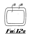
図12は、図1において断面を表示されている型のデバイスを3次元においてどのように実現できるかを示している。図12aは、全体として多角形のNウェル22が、全体として多角形のPウェル20内にどのように存在可能かを示している。表現を簡略化する目的から、図12aでは他のデバイスの特徴は削除されている。Pウェル及びNウェルの両方の表面部分は代わりに円形にすることができる。 FIG. 12 shows how a device of the type whose cross section is displayed in FIG. 1 can be realized in three dimensions. FIG. 12 a shows how a generally polygonal N-well 22 can exist within a generally polygonal P-well 20. For the purpose of simplifying the representation, the features of other devices have been deleted in FIG. 12a. The surface portions of both P-well and N-well can instead be circular.
Nウェル22内では、個々のセル(表示なし)を、円形、多角形、ストライプの形態、又はこれらの形態の組み合わせにすることができる。 Within the N-well 22, individual cells (not shown) can be in the form of a circle, polygon, stripe, or a combination of these forms.
図12bは、複数のPウェル20/Nウェル22構造を備えるデバイスを示しており、それぞれの構造がセル30のクラスタを含んでいる。 FIG. 12 b shows a device comprising a plurality of P-well 20 / N-well 22 structures, each structure containing a cluster of
図1のデバイスの基本的な動作について説明したため、次にその動作パラメータのいくつかの特徴について、更に詳細に説明する。 Having described the basic operation of the device of FIG. 1, some features of its operating parameters will now be described in more detail.
オン状態の性能
閾値電圧を超える正のバイアスがゲートG1及びG2に加えられた時、カソードMOSFETはオンとなり、電子はTmos1を通じてN−ドリフト領域24に供給される。アノード電圧がバイポーラオンセット電圧よりも高い時、アノードからホールが注入される。しかしながら、IGBT又はESTの場合のように、ホールが直接カソード領域に流れる経路は存在しない。その結果、Pウェル領域20の電位は増加する。 When a positive bias exceeding the on-state performance threshold voltage is applied to gates G1 and G2, the cathode MOSFET is turned on and electrons are supplied to N-
Tnpn2のエミッタとして機能するN領域22の濃度は、デバイスをオンにする上で重要な役割を果たし、電荷蓄積型IGBT(CS−IGBT)の場合のように、これはホールのバリアを形成するのに必要な限界を上回る。制御ゲートG1/G2がオンである時、Nウェル22は、Nウェル領域に形成される蓄積領域と、Pベース領域32の反転チャネル32a、32bとを通じて、カソード電位に拘束される。Pウェル20の電位が増加すると、トランジスタTnpn1はオンになる。この結果として、サイリスタの点火が発生する。The concentration of the
電流飽和の特徴
通常、サイリスタ70は制御MOSFETが飽和する前にオンとなる。MOSFETが飽和すると、Nウェル/Pウェル(22+20)電位は増加する。こうした電位の増加は、Pベース32/Nウェル22空乏領域の強化につながる。Nウェル22の濃度はPベース32のものよりも低いため、この空乏は主にNウェル領域に移動する。特定の設計電圧(ドーピング濃度、Nウェルの深さ、Pベースの深さ、及びMOSチャネル飽和特性によって決定される)では、空乏はPウェル/Nウェル接合部23に接触し、この時点でデバイスはクランプされる。このセルフクランプ機能により、アノード電位における任意の更なる増加が、Pウェル/Nウェルドリフト領域(20+24)のみで降下する状態が確保される。 Current Saturation Features Normally,
順方向遮断
このデバイスの順方向遮断電圧能力は、一定の技術の平面IGBTのものよりも大幅に高く、これはPウェル/Nウェルドリフト領域接合部21が、デバイスのエッジを除き、平面に平行であるためである。更に、従来のIGBTでは、深いP+領域のため、空乏領域は基本的にNドリフト領域に移動する。しかしながら、クラスタIGBTでは、Pウェル20による電位共有の結果として、一定の遮断電圧に関して、低いピーク電界が生じる。そのため、一定の遮断能力に関して、図1のクラスタサイリスタデバイスでは、従来のIGBTよりも、ウェーハが遥かに薄くなる。これは順方向降下、スイッチ性能、熱特性、及び安定性に関して、直接的で好ましい意味を有する。 Forward cutoff The forward cutoff voltage capability of this device is significantly higher than that of certain technology planar IGBTs, which means that the P-well / N-well drift region junction 21 is parallel to the plane except for the edge of the device. This is because. Further, in the conventional IGBT, the depletion region basically moves to the N drift region because of the deep P + region. However, in a cluster IGBT, as a result of potential sharing by the P-well 20, a low peak electric field is generated for a constant cutoff voltage. Therefore, with respect to a constant interrupt capability, the cluster thyristor device of FIG. 1 is much thinner than a conventional IGBT. This has a direct and favorable meaning with regard to forward drop, switch performance, thermal properties, and stability.
一定の遮断電圧に関して、このデバイスは2つの方法で設計することができる。 For a constant cut-off voltage, this device can be designed in two ways.
(a)Pウェル20濃度が高い時、Pウェル/Nウェル領域(20+24)では全体の遮断電圧が降下する。 (A) When the concentration of the P well 20 is high, the overall cutoff voltage drops in the P well / N well region (20 + 24).
(b)Pウェル20濃度が低い時、アノードバイアスの増加と共に、Pウェル層は空乏化する。その後、Nウェル(22)/Pベース(32/34)接合部では電圧における任意の更なる増加が降下する。デバイスが「セルフクランプ」機能を有する設計であるため、Nウェル/Pウェルベース空乏領域はPウェル内に延び、これによりNウェル(22)における任意の更なる増加が防止される。 (B) When the concentration of the P well 20 is low, the P well layer is depleted as the anode bias increases. Thereafter, any further increase in voltage drops at the N-well (22) / P base (32/34) junction. Since the device is designed with a “self-clamping” function, the N-well / P-well base depletion region extends into the P-well, thereby preventing any further increase in the N-well (22).
ターンオフ
デバイスのターンオフ性能は、IGBTのものと同様である。制御ゲートG2がオフになった時、Pベース/Nウェル(32+34/22)の電位はセルフクランプが起きるまで増加する。クランプされると、Pウェル(20)の幅が広い性質から、Pベース領域(32+34)にホールを効果的に集めることが可能となる。セルに対称性があり、密に詰まっていることから、デバイスの電流の流れは、MCTとは異なり、あらゆる場合において均一にすることが可能となる。ESTとは異なり、セルフクランプにより、制御MOSFETの電圧がセルフクランプ電圧を超えて上昇しない状態が確保される。 The turn- off performance of the turn- off device is similar to that of the IGBT. When the control gate G2 is turned off, the potential of the P base / N well (32 + 34/22) increases until self-clamping occurs. When clamped, holes can be effectively collected in the P base region (32 + 34) due to the wide nature of the P well (20). Unlike the MCT, the current flow of the device can be uniform in all cases because the cells are symmetrical and densely packed. Unlike EST, self-clamping ensures that the control MOSFET voltage does not rise above the self-clamp voltage.
クラスタIGBT/サイリスタは他の構造とどのように異なるか。 How is a cluster IGBT / thyristor different from other structures?
クラスタIGBT/サイリスタデバイスは、従来のIGBTとはまったく異なる。IGBTの場合、寄生ラッチアップを抑え、必要な遮断電圧能力を達成するために深いP+領域が必要となる。しかしながら、深いP+領域の要件から、カソードセルは、クラスタIGBT/サイリスタのものに比べて遥かに大きくなる。例えば、3μm設計規則に基づくと、DMOS IGBTの最小カソードセル寸法は約36μmだが、CMOSプロセスに基づくクラスタIGBT/サイリスタカソードセルでは15μmである。サブミクロンファインライン(FL)リソグラフィ手法を選択することで、IGBTのカソードセルを縮小することも可能である。FL−IGBT及びFL−ESTの場合は、薄い酸化物がJFET領域上に延びる。こうしたデバイスの優れた順方向遮断安全動作区域FBSOA特性は、静的な条件下で実証されている。しかしながら、高電流及び高電圧が同時に存在する誘導負荷スイッチング条件下では、このデバイスの特性は完全には実証されていないが、短絡性能は劣っている。こうした条件下では、FL−IGBT及びFL−ESTは機能しなくなると考えられる。 Cluster IGBT / Thyristor devices are quite different from conventional IGBTs. In the case of an IGBT, a deep P + region is required to suppress parasitic latchup and achieve the required cut-off voltage capability. However, due to the deep P + region requirement, the cathode cell is much larger than that of the cluster IGBT / thyristor. For example, based on the 3 μm design rule, the minimum cathode cell size for a DMOS IGBT is about 36 μm, but 15 μm for a cluster IGBT / thyristor cathode cell based on a CMOS process. By selecting a submicron fine line (FL) lithography technique, the IGBT cathode cell can be reduced. In the case of FL-IGBT and FL-EST, a thin oxide extends over the JFET region. The superior forward blocking safe operating area FBSOA characteristics of these devices have been demonstrated under static conditions. However, under inductive load switching conditions where high current and high voltage exist simultaneously, the device characteristics have not been fully demonstrated, but short circuit performance is poor. Under these conditions, FL-IGBT and FL-EST are thought to fail.
更に、シミュレーション結果は、クラスタIGBT/サイリスタが優れた性能を発揮するためには、隣接セルとの距離が6μmで十分であることを示している。IGBTの場合、最適な寸法はセルのジオメトリ及び遮断能力に応じて変化し、通常は2kV定格より大きなデバイスでは25μmを上回る。 Further, the simulation results show that a distance of 6 μm from the adjacent cell is sufficient for the cluster IGBT / thyristor to exhibit excellent performance. In the case of IGBTs, the optimal dimensions will vary depending on the cell geometry and blocking capability and are typically above 25 μm for devices larger than 2 kV ratings.
クラスタIGBT/サイリスタの性能は、DMOS−IGBTのものよりも優れている。 The performance of the cluster IGBT / thyristor is superior to that of the DMOS-IGBT.
更に、本発明を実施するデバイス構造は、米国特許第5,293,054号のいて開示されているようなESTとは、2つの点において大きく異なっている。第一に、オン状態で伝導性調節が行われる電荷制御Nエミッタ領域は、Pベース及びPウェル領域を分離する。これにより、このデバイスは、高ドープN+浮遊エミッタ領域を使用する、前記シェカーらが報告したトレンチESTとも異なる。上で述べたあらゆるESTにおいて、電流飽和は、制御MOSFET飽和の結果としてのみ達成される。しかしながら、制御MOSFETは通常、低電圧MOSFETであり、結果として、N+浮遊エミッタの電位が制御MOSFETの絶縁破壊電圧を超えて増加する時、このデバイスは機能しなくなる。クラスタIGBT/サイリスタでは、連続MOSチャネル飽和に加えて、セルフクランプ機能が存在する。その結果、スイッチ条件下であっても、カソード領域の電位は設計セルフクランプ電圧を上回らない。このクランプ電圧はMOSFET絶縁破壊電圧よりも遥かに小さい。Further, the device structure embodying the present invention differs significantly from the EST as disclosed in US Pat. No. 5,293,054 in two respects. First, the charge controlled N emitter region, where conductivity adjustment is performed in the on state, separates the P base and P well regions. This device thus differs from the trench EST reported by Sheker et al., Which uses a highly doped N + floating emitter region. In any EST mentioned above, current saturation is achieved only as a result of control MOSFET saturation. However, the control MOSFET is typically a low voltage MOSFET, and as a result, the device will not function when the potential of the N + floating emitter increases beyond the breakdown voltage of the control MOSFET. In a cluster IGBT / thyristor, in addition to continuous MOS channel saturation, a self-clamping function exists. As a result, the cathode region potential does not exceed the design self-clamp voltage even under switch conditions. This clamp voltage is much smaller than the MOSFET breakdown voltage.
クラスタIGBTはFiBSとどのように異なるか。 How is a cluster IGBT different from FiBS?
(a)上で説明したクラスタIGBT/サイリスタデバイスとは異なり、FiBSのデバイスセルは非対称である。 (A) Unlike the cluster IGBT / thyristor device described above, the device cell of FiBS is asymmetric.
(b)カソードセルの一定の区域及び数に関して、FiBSと比較すると、クラスタIGBT/サイリスタには2倍の数のN+カソード及び制御チャネルが存在する。その結果、FiBSと比較して、このデバイスが順方向降下性能における大幅な改善を示すことが予測される。(B) For a given area and number of cathode cells, there are twice as many N + cathodes and control channels in the cluster IGBT / thyristor compared to FiBS. As a result, it is expected that this device will show a significant improvement in forward descent performance compared to FiBS.
(c)FiBSは3ゲート構造である。NMOSゲートはESTと同様の方法でターンオンを制御するのに使用され、PMOSゲートはターンオフを制御するのに使用される。第3のゲートは、クラスタIGBTと同じく、デバイスをターンオンする。PMOSゲートでの電圧がスイッチ中の遮断を決定する。 (C) FiBS has a three-gate structure. The NMOS gate is used to control turn-on in the same manner as EST, and the PMOS gate is used to control turn-off. The third gate turns on the device, similar to the cluster IGBT. The voltage at the PMOS gate determines the interruption in the switch.
(d)FiBSの処理は、米国特許第5,286,981号において報告されているように、クラスタIGBTのものとは大きく異なる。 (D) FiBS processing differs significantly from that of cluster IGBTs, as reported in US Pat. No. 5,286,981.
(e)「DMOS FiBS」は高ドープN++エミッタを使用する。これはクラスタIGBT/サイリスタには存在しない。(E) “DMOS FiBS” uses highly doped N ++ emitters. This is not present in the cluster IGBT / thyristor.
(f)飽和メカニズムは、IGBT/サイリスタのものと大きく異なっている。つまり、FiBSの場合、飽和はPMOSデバイスをオンにすることで達成される。説明したクラスタIGBT/サイリスタの場合、電流飽和はセルフクランプによって達成される。つまり、Pベース/Nウェル接合部に逆バイアスが加えられ、空乏領域がPベースの下で増加し、Pウェルに接触する。到達した時、セルの電位はクランプされ、Pウェル/Nドリフト接合部は電圧の任意の更なる増加をサポートする。 (F) The saturation mechanism is very different from that of the IGBT / thyristor. That is, in the case of FiBS, saturation is achieved by turning on the PMOS device. For the cluster IGBT / thyristor described, current saturation is achieved by self-clamping. That is, a reverse bias is applied to the P base / N well junction, and the depletion region increases under the P base and contacts the P well. When reached, the cell potential is clamped and the P-well / N drift junction supports any further increase in voltage.
(g)IGCT/FiBSの製造にはエピタキシャル層が必要である。クラスタIGBTは、Pウェル、Nウェル、及びPベースの3重拡散を使用して形成できる。 (G) An epitaxial layer is required for manufacturing IGCT / FiBS. Cluster IGBTs can be formed using P-well, N-well, and P-based triple diffusion.
(h)クラスタIGBTサイリスタは、CMOSシーケンスの開始前にいくつかの拡散を追加し、CMOSプロセスを使用して製造できる。FiBSの製造プロセスはこれとは異なる。結果として、デバイスのゲートパッド区域において、CMOS又は類似物に基づいて、ゲート制御回路を統合することが可能となる。現在の検出及びゲート保護回路をクラスタレベル及びデバイスレベルで統合することも可能となる。更に、キャリア寿命の減少と共に、順方向降下を減らすためにNウェル濃度を増加させることができる。 (H) A cluster IGBT thyristor can be fabricated using a CMOS process with some diffusion added before the start of the CMOS sequence. The manufacturing process for FiBS is different. As a result, it is possible to integrate gate control circuitry based on CMOS or the like in the gate pad area of the device. It is also possible to integrate current detection and gate protection circuits at the cluster level and device level. Furthermore, the N-well concentration can be increased to reduce the forward drop with decreasing carrier lifetime.
上で説明したクラスタカソードセルの構造は、バイポーラ/MOS系統の他のデバイスに応用することもできる。こうしたデバイスの例について次に説明する。 The cluster cathode cell structure described above can also be applied to other devices in the bipolar / MOS system. An example of such a device will now be described.
クラスタEST
図1の基本的なクラスタIGBT/サイリスタ構造に深いP+分離を加えることで、このデバイスの動作をまったく異なるものにすることができる。この場合、デバイスはクラスタESTのような動作をする。この例は、図1と同じで特徴が1つ追加された図2の断面図に表示されている。そのため、以下の説明は、追加された特徴とその動作上の影響とに限られる。 Cluster EST
By adding deep P + isolation to the basic cluster IGBT / thyristor structure of FIG. 1, the operation of this device can be quite different. In this case, the device operates like a cluster EST. This example is shown in the cross-sectional view of FIG. 2 which is the same as FIG. 1 with one feature added. Thus, the following description is limited to the added features and their operational impact.
図2に見られるように、独立したP+分離領域50が図1のクラスタIGBT/サイリスタに追加されている。これは表面18から拡散し、Nウェル22を通じてPウェル内に延びている。この領域50は共通カソードセル金属化部40に結合されている。その結果、Pウェル20は浮遊ではなくなり、カソード電位となる。図1及び図1aのデバイスと比較すると、図2のデバイスの順方向特性は大きく異なる。これは、アノード/Nドリフト領域(14/24)に順方向バイアスが加えられ、ゲートG1、G2がオンとなっている時、ホールがデバイスに注入されるためである。このホールは次にP+分離領域50に向かって流れる。Pウェル20の抵抗に応じて、ホール電流の流れによって、Pウェル20とNウェル22との間の接合部23がオンとなる。これが起こる時、Nウェル22/Pウェル20/Nドリフト領域24を含むNPNトランジスタがオンとなり、結果として、MOS制御エミッタスイッチトサイリスタが形成される。As can be seen in FIG. 2, an independent P + isolation region 50 has been added to the cluster IGBT / thyristor of FIG. This diffuses from the
この変形の結果、領域22にあるセル間のNウェルの濃度を増加させることが可能となる。更に、他のEST構造との比較において、前に説明したセルフクランプ機能により、クラスタESTでは制御MOSFETの機能停止は起こらない。 As a result of this deformation, the concentration of the N well between the cells in the
クラスタ絶縁ベースEST(IBEST)
クラスタESTの順方向特性はPウェル20の抵抗に応じて変化する。Pウェルの抵抗が低い場合、サイリスタのターンオン電圧は高くなる。この制約を克服するためには、図3に示す構成を有するデバイスを製造することができる。このデバイスは図1のものと同じ構造だが、特徴が追加されている。以下の説明は、追加された特徴とその動作上の影響とに限られる。 Cluster insulation base EST (IBEST)
The forward characteristics of the cluster EST change according to the resistance of the P well 20. When the resistance of the P-well is low, the turn-on voltage of the thyristor is high. In order to overcome this limitation, a device having the configuration shown in FIG. 3 can be manufactured. This device has the same structure as that of FIG. 1, but with additional features. The following description is limited to the added features and their operational impact.
図3のデバイスにおいて、P+分離領域50が図2と同様に設けられる。これはPウェル20内のカソードセル30のクラスタを分離する。しかしながら、分離領域50は図2のものとは異なる形で扱われる。Pウェル20に達する領域50の拡散に関連して、N+領域52が隣接する表面18で拡散され、Nウェル22の隣接する表面部22aと領域50自体との両方に交わる。これにより形成されるP+/N+接合部は、非整流であり、上には金属化部54が金属化部40とは分離した状態で重なり、浮遊オーム接点(FOC)が形成される。このFOCはP+領域50をN+領域52cを通じてNウェル22に結合させる。この浮遊オーム接点は、デバイスの電極端子のいずれかと結合していないため、このデバイスは依然として3端子デバイスとなる。In the device of FIG. 3, a P + isolation region 50 is provided as in FIG. This isolates the clusters of
図3のデバイスの動作は以下のようになる。ゲートG1、G2がオンとなると、電子がNドリフト領域24に流れ込む。FOCは電子からホールヘのコンバータのように機能する。Pウェル20は浮遊となっているため、Pウェルの電位は増加し、Nウェル22はPウェル電位に拘束されているため、制御MOSFETでの電位降下が増加する。結果として、電子流の流れが増加する。Nウェル/Pウェル電位の増加に伴い、Pベース/Nウェル(32/22)での降下はセルフクランプが発生するまで増加する。 The operation of the device of FIG. 3 is as follows. When the
トレンチゲートMOSにおけるカソードセルクラスタを使用したIGBT/サイリスタの実施は図4に表示されている。この図は分離領域の提供についても例示している。 An implementation of an IGBT / thyristor using a cathode cell cluster in a trench gate MOS is shown in FIG. This figure also illustrates the provision of a separation region.
図4において、図1のものと同じ又は同様の機能を有する層及び領域については、数字を「100」増やした同じ参照番号で示している。 4, layers and regions having the same or similar functions as those in FIG. 1 are denoted by the same reference numerals with numerals increased by “100”.
図4のデバイス110は、P+基板112を使用した半導体ボディを備え、基板112は共通アノード領域を提供し、この領域でアノード接点116が形成される。Nドリフト領域124はアノード領域の上に存在し、126において反対側の表面118まで延びる。このデバイスは更にPウェル120を備え、この中には領域124から垂直方向に間隔を空け、126において表面まで延びる部分からは横方向に間隔を空けて、Nウェル122が配置される。Pウェル120の表面隣接部120bは、隣接する部分126及び122a間のチャネルを提供する。このチャネルの上にはゲート2が重なる。図4において、ゲート酸化物は黒で表示されている。The
ここで、Pウェル2と呼ばれる領域の存在を無視すると、表示のようにNウェルはカソードセルのクラスタ130を含み、このセルは3つ表示されている。それぞれのセルは同じ対称構造である。このセルは、それぞれのセルのゲート構造と交差する単一のPベース領域132に形成されている。左のセルを見ると、ゲート構造は表面126からNウェル領域122内に延びるトレンチを備える。 Here, ignoring the existence of a region called P well 2, as shown, the N well includes a
ポリシリコンゲートであるゲート1は、トレンチ内に配置され、ゲート酸化物138によって隣接するシリコン材料から分離される。表面に隣接して、N+領域136a及び136bがP−ベース材料132内に形成される。領域132a及び132bは、MOSFETの個々のチャネルを提供し、それぞれはゲートによって、ソース136a又は136bと、Nウェル122の部分122aのドレーンとを有する。図1と同じく、ゲート1はカソード/ソース接点金属化部140からNウェルへの伝導を制御する。図4において、カソード接点は、それぞれのソース領域136a、136bに延びる金属化部によって提供されるものであり、注意点として、表面118において、この接点はN+領域136a、136bとPベース134との間のPN接合部を橋絡する。
動作するデバイスにおいて、この接点金属化部は相互接続され、共通カソード端子が形成され、すべてのゲート1ポリシリコンは金属化によって相互接続される(表示なし)。したがって、すべてのカソードセルはアノードに関して並列で動作する。これまでに説明したこの構造の動作は、基本的に図1及び1aに関して説明したとおりである。 In a working device, this contact metallization is interconnected to form a common cathode terminal, and all
次にPウェル2の提供を含めて考えると、これはPベース領域134を通じてNウェル122内に延びるP+ドープ領域156である。これはカソード金属化部140に接触され、結果として、セルフクランプが達成される分離区域が生じる。Pウェルのいずれかの側に位置するゲートは相互接続の必要がなく、代わりに、別個に電気的に結合させることができる。Considering now including the provision of the P well 2, this is a P + doped
別の変形例は破線で示されており、ここでは、Pウェル領域120内に入り込み、これと結合する深い領域158としてPウェル2が形成される。この場合、領域158は図2の領域50のような分離領域として機能し、このデバイスはESTとなる。 Another variation is shown in broken lines, where the P-well 2 is formed as a
図5はアノードゲートデバイスを表示しており、ここではゲート1がオンの時にゲート2はオフとなり、その逆にもなる。 FIG. 5 shows an anode gate device, where
本発明は他のバイポーラ/MOS構造に応用することも可能である。こうした構造には、「準垂直」デバイス及び横方向デバイスと呼ばれるものが含まれる。次にこうしたデバイスの特徴について図6乃至11を参考にして説明する。こうしたデバイス構造の特徴で、これまでに説明したデバイスと基本的に同じであるものについては、ここで繰り返さない。 The present invention can also be applied to other bipolar / MOS structures. Such structures include what are referred to as “quasi-vertical” devices and lateral devices. Next, the characteristics of such a device will be described with reference to FIGS. Such device structure features that are basically the same as the devices described so far will not be repeated here.
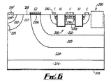
次に説明するすべてのデバイスは、接合部分離(JI)、誘電分離(DI)、2重エピタキシ層誘電分離(DELDI)等の任意の技術において製造することができる。すべてのデバイスは、好ましくは、RESURF(縮小表面フィールド)手法を利用し、横方向絶縁破壊電圧を達成する。すでに説明したデバイスと同じく、クラスタカソードセル構造が利用される。クラスタの主な機能上の原則は、ホールのバリアとして機能する、メインのNウェルのような層を提供することである。これは説明するすべてのデバイスに該当する。 All devices described below can be fabricated in any technique such as junction isolation (JI), dielectric isolation (DI), double epitaxy dielectric isolation (DELDI), and the like. All devices preferably utilize a RESURF (Reduced Surface Field) approach to achieve a lateral breakdown voltage. As with the devices already described, a cluster cathode cell structure is utilized. The main functional principle of the cluster is to provide a main N-well-like layer that acts as a hole barrier. This is true for all devices described.
図6はNウェル222にカソードセルのクラスタ230を有するデバイスを示している。この構造はトレンチゲートであり、主な特徴は図4のものと同じであり、Pウェル2領域は有しない。図6では、表面218へのNドリフト領域224の延長部221において、横方向アノード構造が上部表面218に提供される。このアノード構造は、パンチスルーを防ぐために、領域226内に拡散されたNバッファ領域262を備える。バッファ領域262内には、横方向アノードP+領域214’が拡散され、ここにはアノード接点216’が形成される。このデバイスは下部表面にアノード構造214、216を保持する。アノード216及び216’は、共に結合させること、或いは分離させることが可能である。更に、横方向アノードのみが提供されるように、下部表面のアノードを省略することも可能である。この場合、P+基板も省略することができる。FIG. 6 shows a device having a cluster 230 of cathode cells in an N-
トレンチとして例示されているゲート1は代わりに平面にすることができる。平面として例示されているゲート2は代わりにトレンチにするととができる。カソード(C)は240又はトレンチにおける平面金属化部とすることができる。 The
このカソード構造では、隣接するN+ソース領域236a、236bの間にP+領域264の提供が任意の追加として行われ、関連するカソード接点Cは、表面に出現したP+及びN+領域の間の境界上に延びる。In this cathode structure, the provision of a P + region 264 is provided as an optional addition between adjacent N + source regions 236a, 236b, and the associated cathode contact C is between the P + and N + regions that appear on the surface. Extends on the boundary.
図6では更に、Nウェル222内の横方向ゾーン280に提供することが可能な他の3種類の任意の特徴も例示している。これらは図6乃至6cに例示されている。 FIG. 6 further illustrates three other optional features that can be provided to the
図6aは、Nウェル222へのPウェル256の追加を示しているが、これは浅いためメイン構造のPウェル220に接触しない。カソード接点Cは、好ましくはP+拡散257を通じて、この追加ウェルに形成される。これにより、セルフクランプを達成する分離エリアが提供される。図6b及び6cの任意の特徴では、結果として、それぞれEST及びIBESTデバイスが提供される。FIG. 6a shows the addition of a P-well 256 to the N-well 222, which is shallow and does not contact the main structure P-well 220. FIG. Cathode contact C is formed in this additional well, preferably through P + diffusion 257. This provides a separation area that achieves self-clamping. The optional features of FIGS. 6b and 6c result in EST and IBEST devices, respectively.
図6bは、下方に延びてメインのPウェル220に接触し、図4で158で示すような分離領域を提供する深いP+ウェル258を示している。図6cは、Pウェル220に入り込み、これと接触するように延びるが、更に図3の実施例に関して説明した浮遊オーム接点(FOC)に適合する同様の深いP+ウェル258’を示している。浅い表面隣接N+領域252は、領域258’との非整流接合部を形成し、この領域及び接合部の上には金属化部254が重なる。FIG. 6b shows a deep P + well 258 that extends downward and contacts the main P-well 220 and provides an isolation region as shown at 158 in FIG. FIG. 6 c shows a similar deep P + well 258 ′ extending into and in contact with the P-well 220 but compatible with the floating ohmic contact (FOC) described with respect to the embodiment of FIG. Shallow surface-adjacent N + region 252 forms a non-rectifying junction with region 258 ', and
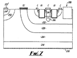
図7は、図6のカソードセル構造の更なる変形例を示している。ここでP+領域264は266において垂直に下方へ延び、分離セルフクランプ区域を提供するために、N−ウェル領域220に入る。この構造のその他の部分は図6と同じである。アノード1及びアノード2は、共に結合させること、或いは分離させることが可能であり、ゲート1及びカソードは両方とも平面又はトレンチにすることができる。FIG. 7 shows a further modification of the cathode cell structure of FIG. Here, the P + region 264 extends vertically downward at 266 and enters the N - well region 220 to provide an isolation self-clamping area. The other parts of this structure are the same as in FIG.
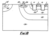
図8は、図6のデバイスの更なる変形例を示している。この変形例では、図6においてPウェル220のチャネル領域220bを制御するゲート2は、Nドリフト領域224からNウェル領域222への電子経路を提供する浮遊オーム接点に置き換えられている。表面226に出現するP−ウェル220の部分220BはP+となり、Nウェル222の接触部分222aはN+となり、金属化接点25Aはこの2つを橋絡する。N+領域222aはクラスタセル構造から横方向に離れている。図6を参考に説明した選択可能なその他の変形例も図8に応用することができる。図8のデバイスはP+基板上に配置できるが、その必要性はない。FIG. 8 shows a further variation of the device of FIG. In this variation, the
図9は、図1のデバイスの横方向バージョンを示している。表示のように、図9の構造は、基本的に半導体ボディ310の上部表面318に隣接して定められている。このボディは最低部にP領域320を有する。P領域320の上では、N領域が最初に形成され、この中で上部表面318からその後のプロセス動作が実行される。横方向のシーケンスにおいて、このデバイスは拡散P+アノード領域314を有し、ここにアノード接点316が形成される。このP+領域自体は、最初のN領域内に拡散された更に広範なNバッファ領域320内に拡散されて存在し、最初のN領域は横方向に離れた2つの部分に区分されている。第1はNドリフト領域322であり、第2はNドリフト領域324である。ドリフト領域324は内部に形成されたアノード構造を有するが、領域322は内部に形成されたカソード構造330を有する。これら2つの領域は分離されているが、MOSFETによって制御可能な状態で結合することができる。FIG. 9 shows a lateral version of the device of FIG. As shown, the structure of FIG. 9 is essentially defined adjacent to the
領域322と324との間では、P+分離領域358が拡散され、これは下にあるP領域320まで延びて入り込んでいる。領域358は2つのドリフト領域を分離する。これらの間の電子の流れは、ゲート酸化物342上に形成されたゲートであるゲート2を有するMOSFETによって制御される。ゲート2は、表面318において、領域322及び324の両方の上で延び、領域358の上でも延びる。Nインプラント359はゲート2の下に提供され、P+領域を通じて延び、Nドリフト領域の隣接部分に入る。Nインプラントは、ゲート2の下のチャネルにおいて多数キャリア濃度を減少させ、これによりMOSFETトランジスタをオンにするために必要な閾値電圧を低下させる。Between
次にNドリフト領域322に形成されたクラスタカソードセル構造330について説明する。Pベース領域332を有し、制御可能な状態でNドリフト領域322と結合させることができるカソードセルがこの中で形成される点において、これは図4を参考にしてすでに説明したものと同様である。クラスタ330のそれぞれのセルはトレンチゲートであるゲート1を備え、これはN+ソース領域336a、336bとNドリフト領域322との間の導通を制御する。このトレンチゲートは、チャネル334a、334bが存在するベース領域322を通じて延び、それぞれのMOSFETチャネルのドレーン322aを提供するNドリフト領域322に入る。ソース(カソード)接点Cは、領域336a、336bに作成される(表面314に出現するN+領域とPベース領域332との間の接合部を橋絡するそれぞれの接点のための金属化部)。Next, the cluster
実際には、カソード接点Cは、ポリシリコントレンチゲートであるゲート1として相互接続され、カソードセルはアノードに関して並列で動作するようになる。ゲート2は、ゲート1と結合させること、或いは別個に結合させることが可能である。ゲート1は平面の形態及びトレンチにおいて実施可能である。カソードCは、平面の代わりとして、トレンチにすることができる。Nドリフト領域324は、Nドリフト領域322とは異なる厚さにすること、或いは異なるドープ処理を施すことが可能である。領域324は、RESURFを使用して、絶縁破壊電圧をサポートするために使用される。図9のデバイスは、優れたオン状態特性と、高い区域効率とを示す。 In practice, the cathode contact C is interconnected as
図10は、図9の横方向デバイスの変形例を示している。アノードドリフト領域324は、ゲート2と協働して表面に形成される浮遊オーム接点を有する。FOCのP+、N+領域343、345は、浅いPウェル341内に形成され、通常通り、浮遊接点金属化部354によって短絡される。N+領域345は、Nインプラント359に向けて配置され、ゲート2は領域345上で延びることに留意されたい。これにより、MOSFETチャネルへの電子の注入が促進され、その結果、オン状態の抵抗が減少する。FIG. 10 shows a variation of the lateral device of FIG. The
図10は、図6において264で示したものに対応する更なる任意の変形例も示している。隣接するカソードセルの隣接するN+領域は、P+領域364によって結合され、共通のカソード接点により結合される。この結果、より多くの導電チャネルが生じ、したがってデバイスを通じた高い電流の流れが生じる。FIG. 10 also shows a further optional variation corresponding to that indicated by 264 in FIG. Adjacent N + regions of adjacent cathode cells are coupled by P + region 364 and are coupled by a common cathode contact. This results in more conductive channels and thus high current flow through the device.
図11は、図8のデバイスの別の変形例を示している。これは前のパラグラフにおいて述べたカソード構造に対する任意の変形例であるが、更に重要なことには、前に説明したようにトレンチ形態で実現されるゲート2を示している。このゲートはP領域320内に延び、ゲートに隣接する領域320c内には強化モードチャネルが形成されてNドリフト領域324及び322がソース及びドレインをそれぞれ提供する。 FIG. 11 shows another variation of the device of FIG. This is an optional variation on the cathode structure described in the previous paragraph, but more importantly shows the
Claims (6)
第2の導電型の第1のウェル領域と、
第1の導電型の第2のウェル領域と、
第2の導電型のドリフト領域と、
第1の導電型のコレクタ領域と、
コレクタ接点と、
を備え、
多数の各ベース領域が前記第1のウェル領域内に配置され、各ベース領域は少なくともその上に配置された少なくとも1つのエミッタを有し、それによって多数のセルを提供し、第1のウェル領域が第2のウェル領域内に配置される半導体デバイスであって、更に、
エミッタ領域と第1のウェル領域との間にMOSFETチャネルを形成し得るようにベース領域上に配置された第1のゲートと、
第1のウェル領域とドリフト領域との間にMOSFETチャネルを形成し得るように第2のウェル領域上に配置された第2のゲートと、
を備え、
前記セルはそれぞれ対称形であり、
前記デバイスの動作中にベース領域と第1のウェル領域との間の接合部の空乏領域が第1のウェル領域と第2のウェル領域との間の接合部まで延び得るように構成され、これにより、第1のウェル領域の電位がコレクタ接点の電位から分離され、ベース領域と第2のウェル領域との間にMOSFETチャネルを形成する必要なくオフにし得るようにした半導体デバイス。 A number of cells, each having a first conductivity type base region having at least one second conductivity type emitter region disposed therein;
A first well region of a second conductivity type;
A second well region of the first conductivity type;
A drift region of a second conductivity type;
A collector region of a first conductivity type;
A collector contact;
With
A number of each base region is disposed within the first well region, each base region having at least one emitter disposed thereon, thereby providing a number of cells, the first well region Is a semiconductor device disposed in the second well region, and
A first gate disposed on the base region so as to form a MOSFET channel between the emitter region and the first well region;
A second gate disposed on the second well region so as to form a MOSFET channel between the first well region and the drift region;
With
Each of the cells is symmetrical;
The depletion region at the junction between the base region and the first well region can extend to the junction between the first well region and the second well region during operation of the device, The semiconductor device in which the potential of the first well region is separated from the potential of the collector contact and can be turned off without the need to form a MOSFET channel between the base region and the second well region.
第2の導電型の第1のウェル領域と、
第1の導電型の第2のウェル領域と、
第2の導電型のドリフト領域と、
第1の導電型のコレクタ領域と、
コレクタ接点と、
を備え、
多数のベース領域が前記第1のウェル領域内に配置され、各ベース領域は少なくともその上に配置された少なくとも1つのエミッタを有し、それによって多数のセルを提供し、第1のウェル領域が第2のウェル領域内に配置される半導体デバイスであって、更に、
エミッタ領域と第1のウェル領域との間にMOSFETチャネルを形成し得るようにベース領域上に配置された第1のゲートと、
前記のウェル領域とドリフト領域との間にMOSFETチャネルを形成し得るように第2のウェル領域上に配置された第2のゲートと、
を備えた半導体デバイスを提供し、
前記セルはそれぞれ対称形であり、
エミッタ領域と第1のウェル領域との間にMOSFETチャネルを形成し、
第1のウェル領域とドリフト領域との間にMOSFETチャネルを形成し、
オン状態で動作中に、ベース領域と第1のウェル領域との間の接合部で形成された空乏領域が、第1のウェル領域と第2のウェル領域との間の接合部まで延び得るように形成され、それにより第1のウェル領域の電位がコレクタ接点の電位の増加から分離されるように半導体デバイスを動作させ、
ベース領域と第2のウェル領域との間にMOSFETチャネルを形成することなく半導体デバイスをオフにすることを特徴とする半導体デバイスの動作方法。 A number of cells, each having a first conductivity type base region having at least one second conductivity type emitter region disposed therein;
A first well region of a second conductivity type;
A second well region of the first conductivity type;
A drift region of a second conductivity type;
A collector region of a first conductivity type;
A collector contact;
With
A number of base regions are disposed within the first well region, each base region having at least one emitter disposed thereon, thereby providing a number of cells, wherein the first well region comprises A semiconductor device disposed in the second well region, further comprising:
A first gate disposed on the base region so as to form a MOSFET channel between the emitter region and the first well region;
A second gate disposed on the second well region so as to form a MOSFET channel between the well region and the drift region;
Providing a semiconductor device comprising:
Each of the cells is symmetrical;
Forming a MOSFET channel between the emitter region and the first well region;
Forming a MOSFET channel between the first well region and the drift region;
During operation in the on state, the depletion region formed at the junction between the base region and the first well region can extend to the junction between the first well region and the second well region. Operating the semiconductor device so that the potential of the first well region is isolated from the increase in potential of the collector contact,
A method of operating a semiconductor device, wherein the semiconductor device is turned off without forming a MOSFET channel between the base region and the second well region.
Applications Claiming Priority (3)
| Application Number | Priority Date | Filing Date | Title |
|---|---|---|---|
| GBGB9921068.4A GB9921068D0 (en) | 1999-09-08 | 1999-09-08 | Bipolar mosfet device |
| GB9921068.4 | 1999-09-08 | ||
| PCT/GB2000/003443 WO2001018876A1 (en) | 1999-09-08 | 2000-09-07 | Bipolar mosfet device |
Publications (3)
| Publication Number | Publication Date |
|---|---|
| JP2003509849A JP2003509849A (en) | 2003-03-11 |
| JP2003509849A5 JP2003509849A5 (en) | 2007-10-18 |
| JP5357370B2 true JP5357370B2 (en) | 2013-12-04 |
Family
ID=10860461
Family Applications (1)
| Application Number | Title | Priority Date | Filing Date |
|---|---|---|---|
| JP2001522599A Expired - Lifetime JP5357370B2 (en) | 1999-09-08 | 2000-09-07 | Semiconductor device |
Country Status (12)
| Country | Link |
|---|---|
| US (1) | US6724043B1 (en) |
| EP (1) | EP1269546B1 (en) |
| JP (1) | JP5357370B2 (en) |
| KR (1) | KR100687079B1 (en) |
| CN (1) | CN1227744C (en) |
| AT (1) | ATE500618T1 (en) |
| AU (1) | AU781099B2 (en) |
| CA (1) | CA2381530C (en) |
| DE (1) | DE60045692D1 (en) |
| DK (1) | DK1269546T3 (en) |
| GB (1) | GB9921068D0 (en) |
| WO (1) | WO2001018876A1 (en) |
Families Citing this family (35)
| Publication number | Priority date | Publication date | Assignee | Title |
|---|---|---|---|---|
| GB0125710D0 (en) * | 2001-10-26 | 2001-12-19 | Koninkl Philips Electronics Nv | Transistor device |
| JP3753692B2 (en) * | 2002-12-20 | 2006-03-08 | ローム株式会社 | Open drain MOSFET and semiconductor integrated circuit device using the same |
| KR100830982B1 (en) | 2004-05-12 | 2008-05-20 | 도요다 지도샤 가부시끼가이샤 | Insulated gate bipolar transistor |
| GB0417749D0 (en) * | 2004-08-10 | 2004-09-08 | Eco Semiconductors Ltd | Improved bipolar MOSFET devices and methods for their use |
| GB0520909D0 (en) * | 2005-10-14 | 2005-11-23 | Eco Semiconductors Ltd | Power semiconductor devices |
| US7582917B2 (en) * | 2006-03-10 | 2009-09-01 | Bae Systems Information And Electronic Systems Integration Inc. | Monolithically integrated light-activated thyristor and method |
| JP4087416B2 (en) * | 2006-04-06 | 2008-05-21 | シャープ株式会社 | Power IC device and manufacturing method thereof |
| KR100880231B1 (en) * | 2007-06-20 | 2009-01-28 | 주식회사 동부하이텍 | Semi-conductor device, and method for fabricating thereof |
| US7700977B2 (en) * | 2007-06-21 | 2010-04-20 | Intersil Americas Inc. | Integrated circuit with a subsurface diode |
| US20110182094A1 (en) * | 2007-08-13 | 2011-07-28 | The Powerwise Group, Inc. | System and method to manage power usage |
| US8619443B2 (en) | 2010-09-29 | 2013-12-31 | The Powerwise Group, Inc. | System and method to boost voltage |
| US8085009B2 (en) | 2007-08-13 | 2011-12-27 | The Powerwise Group, Inc. | IGBT/FET-based energy savings device for reducing a predetermined amount of voltage using pulse width modulation |
| US8120307B2 (en) | 2007-08-24 | 2012-02-21 | The Powerwise Group, Inc. | System and method for providing constant loading in AC power applications |
| US8810190B2 (en) * | 2007-09-14 | 2014-08-19 | The Powerwise Group, Inc. | Motor controller system and method for maximizing energy savings |
| US8698447B2 (en) | 2007-09-14 | 2014-04-15 | The Powerwise Group, Inc. | Energy saving system and method for devices with rotating or reciprocating masses |
| US8558275B2 (en) * | 2007-12-31 | 2013-10-15 | Alpha And Omega Semiconductor Ltd | Sawtooth electric field drift region structure for power semiconductor devices |
| US9620614B2 (en) * | 2007-12-31 | 2017-04-11 | Alpha And Omega Semiconductor Incorporated | Sawtooth electric field drift region structure for power semiconductor devices |
| US8004255B2 (en) * | 2008-08-07 | 2011-08-23 | The Powerwise Group, Inc. | Power supply for IGBT/FET drivers |
| US8698446B2 (en) | 2009-09-08 | 2014-04-15 | The Powerwise Group, Inc. | Method to save energy for devices with rotating or reciprocating masses |
| EP2475888B1 (en) | 2009-09-08 | 2019-04-24 | The Powerwise Group, Inc. | Energy saving system and method for devices with rotating or reciprocating masses |
| US9257525B2 (en) * | 2011-05-13 | 2016-02-09 | Intersil Americas LLC | Systems and methods for forming isolated devices in a handle wafer |
| KR101352766B1 (en) | 2011-12-08 | 2014-01-15 | 서강대학교산학협력단 | The planar gate IGBT with nMOS |
| CN102956687A (en) * | 2012-10-30 | 2013-03-06 | 浙江大学 | SOI-LIGBT (Silicon on Insulator-Lateral Insulated-Gate Bipolar Transistor) device based on double channel structure |
| GB201313126D0 (en) * | 2013-07-23 | 2013-09-04 | Eco Semiconductors Ltd | MOS-Bipolar Device |
| US9293559B2 (en) | 2013-07-31 | 2016-03-22 | Alpha And Omega Semiconductor Incorporated | Dual trench-gate IGBT structure |
| CN104576365B (en) * | 2013-10-25 | 2017-11-21 | 无锡华润上华科技有限公司 | Cluster IGBT preparation method |
| US9123770B2 (en) | 2013-11-18 | 2015-09-01 | Alpha And Omega Semiconductor Incorporated | Charge reservoir IGBT top structure |
| US20150179794A1 (en) * | 2013-12-24 | 2015-06-25 | Hyundai Motor Company | Semiconductor device and method of manufacturing the same |
| CN106711204B (en) * | 2015-11-12 | 2021-01-22 | 上海联星电子有限公司 | IGBT device and manufacturing method thereof |
| CN108022972B (en) * | 2016-11-02 | 2021-07-23 | 全球能源互联网研究院 | Low-state voltage drop IGBT and control method and manufacturing method thereof |
| TWI659539B (en) * | 2018-06-28 | 2019-05-11 | 立錡科技股份有限公司 | High voltage device and manufacturing method thereof |
| CN110504314B (en) * | 2019-08-30 | 2023-03-03 | 电子科技大学 | Groove-type insulated gate bipolar transistor and preparation method thereof |
| CN110459597B (en) * | 2019-08-30 | 2023-02-07 | 电子科技大学 | Groove-type insulated gate bipolar transistor and preparation method thereof |
| CN111933687B (en) * | 2020-07-07 | 2023-04-18 | 电子科技大学 | Lateral power device with high safety working area |
| GB2606383A (en) | 2021-05-06 | 2022-11-09 | Eco Semiconductors Ltd | A semiconductor device |
Family Cites Families (12)
| Publication number | Priority date | Publication date | Assignee | Title |
|---|---|---|---|---|
| DE4121375A1 (en) * | 1991-06-28 | 1993-01-14 | Asea Brown Boveri | DISABLED POWER SEMICONDUCTOR COMPONENT AND METHOD FOR THE PRODUCTION THEREOF |
| JP3163677B2 (en) * | 1991-09-24 | 2001-05-08 | 富士電機株式会社 | Semiconductor device having MISFET controlled thyristor |
| JP3352840B2 (en) * | 1994-03-14 | 2002-12-03 | 株式会社東芝 | Reverse parallel connection type bidirectional semiconductor switch |
| US5493134A (en) * | 1994-11-14 | 1996-02-20 | North Carolina State University | Bidirectional AC switching device with MOS-gated turn-on and turn-off control |
| WO1996036076A1 (en) * | 1995-05-11 | 1996-11-14 | Fuji Electric Co., Ltd. | Emitter switched thyristor |
| JP3200328B2 (en) * | 1995-06-27 | 2001-08-20 | 株式会社日立製作所 | Composite semiconductor device |
| KR0175276B1 (en) * | 1996-01-26 | 1999-02-01 | 김광호 | Power semiconductor device and method of manufacturing the same |
| DE19710487A1 (en) * | 1996-03-13 | 1997-09-18 | Toshiba Kawasaki Kk | Semiconductor module with vertical semiconductor component |
| DE19638769C1 (en) * | 1996-09-21 | 1998-03-05 | Daimler Benz Ag | Emitter controlled thyristor |
| JP3692684B2 (en) * | 1997-02-17 | 2005-09-07 | 株式会社デンソー | Insulated gate field effect transistor and manufacturing method thereof |
| JP4761011B2 (en) * | 1999-05-26 | 2011-08-31 | 株式会社豊田中央研究所 | Semiconductor device having thyristor and method for manufacturing the same |
| JP2001177091A (en) * | 1999-12-07 | 2001-06-29 | Analog & Power Electronics Corp | Latch-controllable insulation gate bipolar transistor |
-
1999
- 1999-09-08 GB GBGB9921068.4A patent/GB9921068D0/en not_active Ceased
-
2000
- 2000-09-07 CA CA2381530A patent/CA2381530C/en not_active Expired - Lifetime
- 2000-09-07 KR KR1020027002998A patent/KR100687079B1/en not_active IP Right Cessation
- 2000-09-07 JP JP2001522599A patent/JP5357370B2/en not_active Expired - Lifetime
- 2000-09-07 DE DE60045692T patent/DE60045692D1/en not_active Expired - Lifetime
- 2000-09-07 AT AT00958828T patent/ATE500618T1/en not_active IP Right Cessation
- 2000-09-07 AU AU70244/00A patent/AU781099B2/en not_active Expired
- 2000-09-07 DK DK00958828.6T patent/DK1269546T3/en active
- 2000-09-07 WO PCT/GB2000/003443 patent/WO2001018876A1/en active IP Right Grant
- 2000-09-07 EP EP00958828A patent/EP1269546B1/en not_active Expired - Lifetime
- 2000-09-07 CN CNB008126763A patent/CN1227744C/en not_active Expired - Lifetime
- 2000-09-07 US US10/070,513 patent/US6724043B1/en not_active Expired - Lifetime
Also Published As
| Publication number | Publication date |
|---|---|
| JP2003509849A (en) | 2003-03-11 |
| DK1269546T3 (en) | 2011-06-27 |
| GB9921068D0 (en) | 1999-11-10 |
| CN1227744C (en) | 2005-11-16 |
| KR100687079B1 (en) | 2007-02-27 |
| US6724043B1 (en) | 2004-04-20 |
| CN1373905A (en) | 2002-10-09 |
| EP1269546A1 (en) | 2003-01-02 |
| KR20020032567A (en) | 2002-05-03 |
| ATE500618T1 (en) | 2011-03-15 |
| AU781099B2 (en) | 2005-05-05 |
| EP1269546B1 (en) | 2011-03-02 |
| AU7024400A (en) | 2001-04-10 |
| DE60045692D1 (en) | 2011-04-14 |
| CA2381530A1 (en) | 2001-03-15 |
| WO2001018876A1 (en) | 2001-03-15 |
| CA2381530C (en) | 2012-07-10 |
Similar Documents
| Publication | Publication Date | Title |
|---|---|---|
| JP5357370B2 (en) | Semiconductor device | |
| US6051850A (en) | Insulated gate bipolar junction transistors having built-in freewheeling diodes therein | |
| US6091086A (en) | Reverse blocking IGBT | |
| US6303410B1 (en) | Methods of forming power semiconductor devices having T-shaped gate electrodes | |
| US11393901B2 (en) | Cell layouts for MOS-gated devices for improved forward voltage | |
| EP3025373B1 (en) | Mos-bipolar device | |
| US5381025A (en) | Insulated gate thyristor with gate turn on and turn off | |
| US5757034A (en) | Emitter switched thyristor | |
| US6137122A (en) | Latch-up controllable insulated gate bipolar transistor | |
| JPH0851197A (en) | Mos control thyristor having electric current saturation property | |
| JP2009512207A (en) | Power semiconductor devices | |
| EP0540017B1 (en) | MOS gate controlled thyristor | |
| WO1991003078A1 (en) | Insulated gate thyristor with gate turn on and turn off | |
| CN111668212A (en) | Semiconductor device with a plurality of semiconductor chips | |
| JP2000311998A (en) | Insulated gate turn-off thyristor | |
| US11610987B2 (en) | NPNP layered MOS-gated trench device having lowered operating voltage | |
| US6727527B1 (en) | Reverse blocking IGBT | |
| JPH10229192A (en) | Semiconductor switch element | |
| JPH09129863A (en) | Emitter switch thyristor | |
| EP4187615A1 (en) | Npnp layered mos-gated trench device having lowered operating voltage | |
| JP3342944B2 (en) | Horizontal high voltage semiconductor device | |
| GB2606383A (en) | A semiconductor device | |
| JP2629434B2 (en) | Semiconductor device with anode short conductivity modulation type MISFET | |
| JPH06302810A (en) | Semiconductor device | |
| JPH0778965A (en) | High breakdown voltage semiconductor element |
Legal Events
| Date | Code | Title | Description |
|---|---|---|---|
| A711 | Notification of change in applicant |
Free format text: JAPANESE INTERMEDIATE CODE: A711 Effective date: 20040629 |
|
| A521 | Request for written amendment filed |
Free format text: JAPANESE INTERMEDIATE CODE: A821 Effective date: 20040629 |
|
| A521 | Request for written amendment filed |
Free format text: JAPANESE INTERMEDIATE CODE: A523 Effective date: 20070827 |
|
| A621 | Written request for application examination |
Free format text: JAPANESE INTERMEDIATE CODE: A621 Effective date: 20070827 |
|
| A131 | Notification of reasons for refusal |
Free format text: JAPANESE INTERMEDIATE CODE: A131 Effective date: 20110920 |
|
| A601 | Written request for extension of time |
Free format text: JAPANESE INTERMEDIATE CODE: A601 Effective date: 20111219 |
|
| A602 | Written permission of extension of time |
Free format text: JAPANESE INTERMEDIATE CODE: A602 Effective date: 20111227 |
|
| A521 | Request for written amendment filed |
Free format text: JAPANESE INTERMEDIATE CODE: A523 Effective date: 20120321 |
|
| A131 | Notification of reasons for refusal |
Free format text: JAPANESE INTERMEDIATE CODE: A131 Effective date: 20120731 |
|
| A601 | Written request for extension of time |
Free format text: JAPANESE INTERMEDIATE CODE: A601 Effective date: 20121025 |
|
| A602 | Written permission of extension of time |
Free format text: JAPANESE INTERMEDIATE CODE: A602 Effective date: 20121101 |
|
| A601 | Written request for extension of time |
Free format text: JAPANESE INTERMEDIATE CODE: A601 Effective date: 20121128 |
|
| A602 | Written permission of extension of time |
Free format text: JAPANESE INTERMEDIATE CODE: A602 Effective date: 20121205 |
|
| A521 | Request for written amendment filed |
Free format text: JAPANESE INTERMEDIATE CODE: A523 Effective date: 20121220 |
|
| A131 | Notification of reasons for refusal |
Free format text: JAPANESE INTERMEDIATE CODE: A131 Effective date: 20130122 |
|
| A601 | Written request for extension of time |
Free format text: JAPANESE INTERMEDIATE CODE: A601 Effective date: 20130422 |
|
| A602 | Written permission of extension of time |
Free format text: JAPANESE INTERMEDIATE CODE: A602 Effective date: 20130430 |
|
| A601 | Written request for extension of time |
Free format text: JAPANESE INTERMEDIATE CODE: A601 Effective date: 20130521 |
|
| A602 | Written permission of extension of time |
Free format text: JAPANESE INTERMEDIATE CODE: A602 Effective date: 20130528 |
|
| TRDD | Decision of grant or rejection written | ||
| A01 | Written decision to grant a patent or to grant a registration (utility model) |
Free format text: JAPANESE INTERMEDIATE CODE: A01 Effective date: 20130820 |
|
| A61 | First payment of annual fees (during grant procedure) |
Free format text: JAPANESE INTERMEDIATE CODE: A61 Effective date: 20130830 |
|
| R150 | Certificate of patent or registration of utility model |
Free format text: JAPANESE INTERMEDIATE CODE: R150 Ref document number: 5357370 Country of ref document: JP Free format text: JAPANESE INTERMEDIATE CODE: R150 |
|
| R250 | Receipt of annual fees |
Free format text: JAPANESE INTERMEDIATE CODE: R250 |
|
| R250 | Receipt of annual fees |
Free format text: JAPANESE INTERMEDIATE CODE: R250 |
|
| R250 | Receipt of annual fees |
Free format text: JAPANESE INTERMEDIATE CODE: R250 |
|
| R250 | Receipt of annual fees |
Free format text: JAPANESE INTERMEDIATE CODE: R250 |
|
| R250 | Receipt of annual fees |
Free format text: JAPANESE INTERMEDIATE CODE: R250 |
|
| EXPY | Cancellation because of completion of term |