JP5332482B2 - Electro-optical device and electronic apparatus - Google Patents
Electro-optical device and electronic apparatus Download PDFInfo
- Publication number
- JP5332482B2 JP5332482B2 JP2008263143A JP2008263143A JP5332482B2 JP 5332482 B2 JP5332482 B2 JP 5332482B2 JP 2008263143 A JP2008263143 A JP 2008263143A JP 2008263143 A JP2008263143 A JP 2008263143A JP 5332482 B2 JP5332482 B2 JP 5332482B2
- Authority
- JP
- Japan
- Prior art keywords
- light
- frame
- electro
- liquid crystal
- shielding film
- Prior art date
- Legal status (The legal status is an assumption and is not a legal conclusion. Google has not performed a legal analysis and makes no representation as to the accuracy of the status listed.)
- Expired - Fee Related
Links
Images


Abstract
Description
例えば液晶プロジェクタのライトバルブとして用いられ、例えば液晶パネル等の電気光学パネルが実装ケースに実装或いは収容されてなる電気光学装置、及び該電気光学装置を備えた、例えば液晶プロジェクタ等の電子機器の技術分野に関する。 For example, an electro-optical device that is used as a light valve of a liquid crystal projector, and an electro-optical panel such as a liquid crystal panel is mounted or accommodated in a mounting case, and a technology of an electronic device such as a liquid crystal projector that includes the electro-optical device Related to the field.
この種の電気光学装置は、液晶パネル等の電気光学パネルが実装ケースに実装或いは収容されてなり、例えば液晶プロジェクタ等のライトバルブとして用いられる。実装ケースは、例えば、フレームと板状の部材とから構成され、電気光学パネルはフレームによって額縁状にその周縁から覆われ、板状の部材に載置されて収容される。例えば特許文献1や2によれば、実装ケース内において液晶パネルに、液晶プロジェクタにおける投射光が入出射される光入射側及び光出射側の両表面に対して夫々遮光板が設けられる。
In this type of electro-optical device, an electro-optical panel such as a liquid crystal panel is mounted or accommodated in a mounting case, and is used as, for example, a light valve of a liquid crystal projector or the like. The mounting case includes, for example, a frame and a plate-like member, and the electro-optical panel is covered in a frame shape from the periphery by the frame and is placed on and accommodated on the plate-like member. For example, according to
例えば特許文献1から3に開示されるように、実装ケースにおいてフレーム或いは板状の部材は遮光性材料により光入射側の表面部分が形成される。また、電気光学パネルには基板上に有効画面となる領域を規定する額縁状の遮光膜が、複数の画素が配置された画素領域の周縁に設けられる。例えばプロジェクタにおいて、投射光のうち有効画面外となる領域、即ち電気光学パネルの画素領域の周辺に向かって進行する光は、実装ケースの光入射側における表面部分、及び電気光学パネル内の遮光膜によって遮光される。
For example, as disclosed in
また、電気光学パネルの一例である液晶パネルでは、当該液晶パネルが液晶プロジェクタにおけるライトバルブとして用いられる場合、スクリーン上に拡大投射された像に粉塵の像が映り込まないように、ライトバルブの表面へのごみや埃等(以下、単に「粉塵」という。)の付着を防止する防塵用基板が設けられることが多い。 Further, in a liquid crystal panel which is an example of an electro-optical panel, when the liquid crystal panel is used as a light valve in a liquid crystal projector, the surface of the light valve is prevented so that an image of dust is not reflected in an image projected and enlarged on the screen. In many cases, a dustproof substrate is provided to prevent adhesion of dust, dust, etc. (hereinafter simply referred to as “dust”).
上述したような実装ケースにおいて特に光入射側の表面部分は、遮光性を向上させるために光の反射率の比較的高い材料により形成されることがある。この場合、実装ケースの光入射側の表面部分に入射した光が反射されると、この光入射側に電気光学装置外に配置された偏光板の支持部材等に対して反射された光が進行し、再反射されることにより画素領域に迷光となって進行する事態が生じる。よって、このような迷光が画素領域から出射する有効画面を表示する光に多量に紛れ込むことにより表示品質が劣化するおそれがある。 In the mounting case as described above, in particular, the surface portion on the light incident side may be formed of a material having a relatively high light reflectance in order to improve the light shielding property. In this case, when the light incident on the light incident side surface portion of the mounting case is reflected, the light reflected on the support member of the polarizing plate disposed outside the electro-optical device on the light incident side proceeds. However, the re-reflection causes a situation in which the pixel region proceeds as stray light. Therefore, the display quality may be deteriorated by such a large amount of stray light being mixed into the light that displays the effective screen emitted from the pixel region.
本発明は、例えば上述した問題点に鑑みなされたものであり、迷光を少なくすることにより高品質な表示を行うことが可能な電気光学装置及びこのような電気光学装置を備えてなる液晶プロジェクタ等の電子機器を提供することを課題とする。 The present invention has been made in view of the above-described problems, for example, an electro-optical device capable of performing high-quality display by reducing stray light, and a liquid crystal projector including such an electro-optical device. It is an object to provide an electronic device.
本発明の電気光学装置は上記課題を解決するために、電気光学物質を挟持する一対の基板と、該一対の基板の少なくとも一方の基板の前記電気光学物質とは反対側に設けられた他の基板と、前記一対の基板の少なくとも一方の基板上に設けられ、複数の画素が配置された画素領域の周縁に額縁状に形成された第1の遮光膜と、前記他の基板上に前記第1の遮光膜の外周に沿って額縁状に形成された第2の遮光膜とを有する電気光学パネルと、前記電気光学パネルを収容するフレームと、該フレームの前記光入射側に装着され、前記画素領域に対応して設けられた窓部を有し、前記第2の遮光膜と重なるように設けられたカバー部材とを有する実装ケースとを備え、前記カバー部材の少なくとも光入射側の面は、前記第1及び第2の遮光膜よりも光の反射率の低い材料により形成されると共に、前記フレームよりも光の反射率の高い材料により形成されている。 In order to solve the above problems, an electro-optical device according to the present invention includes a pair of substrates that sandwich an electro-optical material, and at least one of the pair of substrates that is provided on the opposite side of the electro-optical material. A substrate, a first light-shielding film provided on at least one of the pair of substrates and formed in a frame shape on a periphery of a pixel region in which a plurality of pixels are disposed, and the first light-shielding film on the other substrate An electro-optical panel having a second light-shielding film formed in a frame shape along the outer periphery of the one light-shielding film , a frame accommodating the electro-optical panel, and mounted on the light incident side of the frame, A mounting case having a window provided corresponding to the pixel region and having a cover member provided so as to overlap the second light-shielding film, and at least a surface on the light incident side of the cover member is , than the first and second light-blocking film Rutotomoni formed by a material having a low light reflectivity is formed by a material having high light reflectivity than the frame.
本発明の電気光学装置によれば、例えば液晶パネル等の電気光学パネルが実装ケース内に収容される。一例として、電気光学パネルとして液晶パネルでは、画素領域において各画素の単位で印加される電圧レベルに応じて、一対の基板間に挟持された電気光学物質である液晶において光を変調する。このような液晶パネルを有する電気光学装置たる液晶装置を、例えば液晶プロジェクタのライトバルブとして用いる場合には、光源より投射光が供給され液晶パネルに入射され、液晶において変調された光が表示光として出射されることにより表示が行われる。 According to the electro-optical device of the present invention, for example, an electro-optical panel such as a liquid crystal panel is accommodated in the mounting case. As an example, in a liquid crystal panel as an electro-optical panel, light is modulated in a liquid crystal that is an electro-optical material sandwiched between a pair of substrates in accordance with a voltage level applied in units of each pixel in a pixel region. When a liquid crystal device as an electro-optical device having such a liquid crystal panel is used as, for example, a light valve of a liquid crystal projector, projection light is supplied from a light source and incident on the liquid crystal panel, and light modulated in the liquid crystal is used as display light. Display is performed by being emitted.
一対の基板の少なくとも一方の基板上には、画素領域の周縁に額縁状の第1の遮光膜が形成される。第1の遮光膜により、画素領域から出射される光により表示される有効画面の領域を規定する。また、例えば防塵用基板である他の基板上には、第1の遮光膜に対応して第2の遮光膜が額縁状のパターンで形成される。よって、例えばプロジェクタにおいて投射光は、電気光学パネルにおいて画素領域に対して入射可能となっており、画素領域外の周辺に向かって進行する光は第1及び第2の遮光膜により遮光される。 A frame-shaped first light-shielding film is formed on the periphery of the pixel region on at least one of the pair of substrates. The first light-shielding film defines an effective screen area displayed by light emitted from the pixel area. For example, on the other substrate which is a dustproof substrate, a second light shielding film is formed in a frame-like pattern corresponding to the first light shielding film. Therefore, for example, in the projector, the projection light can enter the pixel region in the electro-optical panel, and the light traveling toward the periphery outside the pixel region is shielded by the first and second light shielding films.
電気光学パネルに対して、実装ケースの窓から光がその画素領域に対して入射されるが、画素領域外に向かって進行する光は実装ケースの光入射側の表面部分においても遮光される。本発明の電気光学装置では、実装ケースにおいて光入射側の表面部分は少なくとも部分的に第1及び第2の遮光膜よりも光の反射率の低い材料により形成される。即ち、本発明の電気光学装置に対して光の入射される側に、第1及び第2の遮光膜よりもより広く面する実装ケースの光入射側の表面部分においては、少なくとも部分的に第1及び第2の遮光膜よりも光が反射され難いように形成される。よって、実装ケースの光入射側の表面部分において、画素領域外の周辺に向かって進行し表示に寄与しない光の反射を抑制することができる。従って、実装ケースの光入射側の表面部分で反射した光が、電気光学装置外においてその光入射側に配置された部材(例えば偏光板の支持部材等)により再反射されて迷光が生じるのを抑制することができる。その結果、多量の迷光が画素領域から出射される表示光に紛れ込む事態をより有効に防止することが可能となる。 Light enters the pixel area of the electro-optical panel from the window of the mounting case, but the light traveling toward the outside of the pixel area is also blocked by the surface portion on the light incident side of the mounting case. In the electro-optical device of the present invention, the surface portion on the light incident side in the mounting case is at least partially formed of a material having a light reflectance lower than that of the first and second light shielding films. In other words, the surface portion on the light incident side of the mounting case that faces the light incident side of the electro-optical device of the present invention more widely than the first and second light-shielding films is at least partially the first. It is formed so that light is less likely to be reflected than the first and second light shielding films. Therefore, it is possible to suppress reflection of light that travels toward the periphery outside the pixel region and does not contribute to display on the surface portion on the light incident side of the mounting case. Therefore, the light reflected by the surface portion on the light incident side of the mounting case is re-reflected by a member (for example, a support member for the polarizing plate) disposed on the light incident side outside the electro-optical device, and stray light is generated. Can be suppressed. As a result, it is possible to more effectively prevent a large amount of stray light from being mixed into the display light emitted from the pixel region.
ここに、例えばプロジェクタにおいて投射光は、画素領域の中央に向かうほど光量が多くなるようにしぼりがかけられた強力な光で投射される。即ちこの場合、電気光学装置においては、画素領域の中央に向かうほど光量が多くなるような光が入射される。よって、画素領域の縁付近では画素領域外よりも電気光学装置に入射される光の光量は多くなる。従って、実装ケースの光入射側の表面部分の反射率を低くすると、画素領域の縁付近に進行する強力な光に対する電気光学装置における遮光性能が劣化するおそれがある。 Here, for example, in a projector, the projection light is projected with powerful light that is reduced so that the amount of light increases toward the center of the pixel region. That is, in this case, in the electro-optical device, light that increases in amount as it goes toward the center of the pixel region is incident. Therefore, the amount of light incident on the electro-optical device is larger near the edge of the pixel region than outside the pixel region. Accordingly, if the reflectance of the surface portion on the light incident side of the mounting case is lowered, the light shielding performance of the electro-optical device against strong light traveling near the edge of the pixel region may be deteriorated.
本発明の電気光学装置では、第1及び第2の遮光膜の光の反射率が比較的高くなるように形成することで、実装ケースの光入射側の表面部分の反射率を低くするためにその遮光性能が劣化しても、画素領域の縁付近に進行する強力な光を第1及び第2の遮光膜で反射してより確実に遮光することができる。従って、画素領域の縁付近に進行する強力な光が入射されることで電気光学パネル内の温度が顕著に上昇し、そのために電気光学装置の表示品質が劣化するのをより確実に防止することができる。 In the electro-optical device of the present invention, the light reflectance of the surface of the mounting case on the light incident side is reduced by forming the first and second light shielding films so that the light reflectance is relatively high. Even if the light shielding performance is deteriorated, the strong light traveling near the edge of the pixel region can be reflected by the first and second light shielding films and more reliably shielded. Accordingly, it is possible to more reliably prevent the temperature in the electro-optical panel from being significantly increased by the incident of powerful light traveling near the edge of the pixel region, and thus the display quality of the electro-optical device to be deteriorated. Can do.
従って、本発明の電気光学装置では表示品質を向上させて、高品質な表示を行うことが可能となる。 Therefore, the electro-optical device according to the present invention can improve display quality and perform high-quality display.
本発明の電気光学装置の一態様では、前記第2の遮光膜は、前記他の基板上において前記第1の遮光膜よりも前記画素領域に対して少なくとも部分的に外周側に位置するように形成される。 In an aspect of the electro-optical device according to the aspect of the invention, the second light shielding film may be located at least partially on the outer peripheral side with respect to the pixel region with respect to the first light shielding film on the other substrate. It is formed.
この態様では、電気光学パネルにおいて第2の遮光膜は一部において第1の遮光膜に対して重なりつつ、他部において第1の遮光膜よりも画素領域に対して外周側に配置される。よって、電気光学パネルに対して画素領域外に向かって進行する光について、第1及び第2の遮光膜により、互いに重なる部分で光漏れが生じるのを防止しつつより広い領域で遮光することが可能となる。従って、画素領域の縁付近に進行する強力な光を第1及び第2の遮光膜でより確実に遮光することができる。 In this aspect, in the electro-optical panel, the second light-shielding film partially overlaps the first light-shielding film, and the other part is disposed on the outer peripheral side with respect to the pixel region than the first light-shielding film. Therefore, the light traveling toward the outside of the pixel region with respect to the electro-optical panel can be shielded by a first and second light shielding film in a wider region while preventing light leakage from occurring in the overlapping portion. It becomes possible. Therefore, the powerful light traveling near the edge of the pixel region can be more reliably shielded by the first and second light shielding films.
本発明の電気光学装置の他の態様では、前記実装ケースは、前記電気光学パネルをその周縁部側から包囲する開口部を有するフレームと、該開口部を覆うように前記フレームに対して前記光入射側に装着され、前記画素領域に対応する第1の窓部を有する第1のカバー部材と、前記開口部を覆うように前記フレームに対して前記光入射側と反対側の光出射側に装着され、前記画素領域に対応する第2の窓部を有する第2のカバー部材とを備え、前記第1のカバー部材及び前記フレームのうち少なくとも一方は、前記光入射側の面が少なくとも部分的に前記第1及び第2の遮光膜よりも光の反射率の低い材料により形成される。 In another aspect of the electro-optical device according to the aspect of the invention, the mounting case includes a frame having an opening that surrounds the electro-optical panel from a peripheral edge side thereof, and the light with respect to the frame so as to cover the opening. A first cover member mounted on the incident side and having a first window corresponding to the pixel region; and a light emitting side opposite to the light incident side with respect to the frame so as to cover the opening. And a second cover member having a second window portion corresponding to the pixel region, and at least one of the first cover member and the frame has at least a partial surface on the light incident side. Further, it is formed of a material having a light reflectance lower than that of the first and second light shielding films.
この態様では、フレームは、電気光学パネルを収容するための開口を規定する開口部を有する。実装ケース内において、電気光学パネルはその周縁部側からフレームの開口部に包囲され、その開口内に収容される。第1及び第2のカバー部材は夫々、開口部による開口を覆うようにフレームに対して光の入出射側の各々に装着される。第1及び第2のカバー部材では、第1及び第2の窓部により夫々、投射光等の表示に寄与する光が画素領域に入出射することが可能なように、第1及び第2の窓の各々が規定される。 In this aspect, the frame has an opening that defines an opening for accommodating the electro-optical panel. In the mounting case, the electro-optic panel is surrounded by the opening of the frame from the peripheral edge side and is accommodated in the opening. Each of the first and second cover members is attached to each of the light incident / exit sides with respect to the frame so as to cover the opening formed by the opening. In the first and second cover members, the first and second window parts allow the light contributing to display such as projection light to enter and exit the pixel region, respectively. Each of the windows is defined.
この態様では、フレーム及び第1のカバー部材のうち少なくとも一方において、その光入射側に面する表面部分は少なくとも部分的に、第1及び第2の遮光膜よりも光の反射率の低い材料により形成される。従って、実装ケースの光入射側の表面部分において、フレーム及び第1のカバー部材のうち少なくとも一方の表面部分は少なくとも部分的に、第1及び第2の遮光膜よりも光が反射され難いように形成することができる。従って、実装ケースの光入射側の表面部分で反射する光に起因する迷光の発生を抑制することが可能となる。 In this aspect, in at least one of the frame and the first cover member, the surface portion facing the light incident side is at least partially made of a material having a lower light reflectivity than the first and second light shielding films. It is formed. Therefore, in the surface portion on the light incident side of the mounting case, at least one surface portion of the frame and the first cover member is at least partially less likely to reflect light than the first and second light shielding films. Can be formed. Therefore, it is possible to suppress the generation of stray light caused by the light reflected by the surface portion on the light incident side of the mounting case.
この態様では、第1のカバー部材において光の反射率はフレームとは別個に調整することができる。従って、光の反射率を調整することで第1のカバー部材では、フレームと別個に光を反射され易く調整したり、またその逆の調整も容易に行うことができる。ここに、第1のカバー部材の光入射側の表面部分は、フレームよりもより広く面するため、フレームよりは光の反射率が高くなるように形成するのが好ましい。これにより、実装ケースにおいて光入射側の表面部分では、より広く電気光学装置の光の入射される側に面する第1のカバー部材において、画素領域外の周辺に向かって進行し表示に寄与しない光をより多く反射させることができる。 In this aspect, the light reflectance of the first cover member can be adjusted separately from the frame. Therefore, by adjusting the light reflectance, the first cover member can be adjusted so that light is easily reflected separately from the frame, and vice versa. Here, since the surface portion on the light incident side of the first cover member faces wider than the frame, it is preferable to form the first cover member so that the reflectance of light is higher than that of the frame. Accordingly, in the surface portion on the light incident side in the mounting case, the first cover member that faces the light incident side of the electro-optical device more widely proceeds toward the periphery outside the pixel region and does not contribute to display. More light can be reflected.
この、実装ケースのフレームに対して第1及び第2のカバー部材が装着される態様では、前記第1の窓部は、前記第1及び第2の遮光膜よりも前記画素領域に対して部分的に外周側に位置するように形成されるように構成してもよい。 In the aspect in which the first and second cover members are attached to the frame of the mounting case, the first window portion is a part of the pixel region with respect to the first and second light shielding films. Alternatively, it may be configured so as to be positioned on the outer peripheral side.
このように構成すれば、第1のカバー部材の第1の窓部よりも第1及び第2の遮光膜の各々は部分的にそれよりも内側に配置される。第1の窓部の光入射側の表面部分は、上述したように第1及び第2の遮光膜よりも光の反射率の低い材料により形成されるのが好ましい。よって、このように光の反射性能が低下した第1の窓部とは重ならない第1及び第2の遮光膜の各々の部分で、画素領域の縁付近に進行する光を反射させることで、より確実に遮光することができる。また、このように画素領域の縁付近に進行する光を第1及び第2の遮光膜で反射することで、投射光等の電気光学装置外から画素領域に対して進行する光の進路に近似しつつ、光源側に逆行する方向に進行させることが可能となる。従って、画素領域の縁付近に進行する光が第1及び第2の遮光膜で反射されることに起因する迷光の発生を抑制することができる。 If comprised in this way, each of the 1st and 2nd light shielding film will be arrange | positioned partially inside it rather than the 1st window part of a 1st cover member. The surface portion on the light incident side of the first window portion is preferably formed of a material having a light reflectance lower than that of the first and second light shielding films as described above. Therefore, by reflecting the light traveling in the vicinity of the edge of the pixel region at each portion of the first and second light shielding films that do not overlap with the first window portion in which the light reflection performance is thus reduced, The light can be shielded more reliably. In addition, the light traveling near the edge of the pixel region is reflected by the first and second light-shielding films, thereby approximating the path of light traveling from outside the electro-optical device such as projection light to the pixel region. However, it is possible to proceed in the direction going back to the light source side. Therefore, it is possible to suppress the generation of stray light caused by the light traveling near the edge of the pixel region being reflected by the first and second light shielding films.
また、一方で第1の窓部を第1及び第2の遮光膜の各々と部分的に重なるように配置することで、電気光学パネルに対して画素領域外に向かって進行する光について、第1の窓部に加えて第1及び第2の遮光膜により、互いに重なる部分で光漏れが生じるのを防止しつつより広い領域で遮光することが可能となる。 On the other hand, by arranging the first window part so as to partially overlap each of the first and second light shielding films, the light traveling toward the outside of the pixel region with respect to the electro-optical panel is reduced. With the first and second light shielding films in addition to the one window portion, it is possible to shield light in a wider area while preventing light leakage from occurring in the overlapping portions.
ここに既に説明したように、画素領域の中央に向かうほど光量が多くなるようにしぼりがかけられた強力な光で投射される投射光等について、第1及び第2の遮光膜の各々の部分で、画素領域の縁付近に進行する強力な光が反射され、それよりも画素領域の外側に向かって進行し光量がより少ない光が第1の窓部で反射される。従って、電気光学パネル内の温度上昇を抑制しつつ、実装ケースにおける光の反射に起因する迷光の発生をより確実に抑制することが可能となる。 As already described here, each portion of the first and second light-shielding films with respect to the projection light and the like projected with powerful light that has been reduced so that the amount of light increases toward the center of the pixel region. Thus, strong light traveling near the edge of the pixel region is reflected, and light traveling toward the outside of the pixel region and having a smaller amount of light is reflected by the first window portion. Accordingly, it is possible to more reliably suppress the generation of stray light due to the reflection of light in the mounting case while suppressing the temperature rise in the electro-optical panel.
或いは実装ケースのフレームに対して第1及び第2のカバー部材が装着される態様では、前記第1のカバー部材の前記光入射側の面は、少なくとも部分的に、前記フレームよりも光の反射率が高くなるような材料により形成されるように構成してもよい。 Alternatively, in the aspect in which the first and second cover members are attached to the frame of the mounting case, the light incident side surface of the first cover member reflects light more than the frame at least partially. You may comprise so that it may form with the material from which a rate becomes high.
このように構成すれば、既に説明したように、実装ケースにおいて光入射側の表面部分では、より広く電気光学装置の光の入射される側に面する第1のカバー部材において、画素領域外の周辺に向かって進行し表示に寄与しない光をより多く反射させることができる。従って、電気光学パネルに対してより多くの光が入射されることによる、電気光学パネル内の温度上昇をより有効に抑制することが可能となる。 According to this configuration, as already described, the surface portion on the light incident side in the mounting case has a wider area outside the pixel region in the first cover member that faces the light incident side of the electro-optical device more widely. More light that travels toward the periphery and does not contribute to display can be reflected. Accordingly, it is possible to more effectively suppress a temperature rise in the electro-optical panel due to more light entering the electro-optical panel.
本発明の電気光学装置の他の態様では、前記実装ケースは、前記窓部を有し、前記電気光学パネルをその周縁部側から包囲するフレームを備え、前記フレームにおける前記光入射側の面が少なくとも部分的に前記第1及び第2の遮光膜よりも光の反射率の低い材料により形成される。 In another aspect of the electro-optical device according to the aspect of the invention, the mounting case includes a window that includes the window portion and surrounds the electro-optical panel from a peripheral portion side thereof, and the light incident side surface of the frame is At least partially, it is formed of a material having a light reflectance lower than that of the first and second light shielding films.
この態様では、実装ケース内において、電気光学パネルはその周縁部側からフレームに包囲されて収容される。フレームは、光を画素領域に入射することが可能な窓が窓部によって規定される。 In this aspect, in the mounting case, the electro-optical panel is enclosed and accommodated in the frame from the peripheral edge side. In the frame, a window that allows light to enter the pixel region is defined by the window portion.
この態様では、フレームにおいて光入射側の表面部分は少なくとも部分的に、第1及び第2の遮光膜よりも光の反射率の低い材料により形成される。従って、実装ケースの光入射側の表面部分において、フレームの表面部分が少なくとも部分的に第1及び第2の遮光膜よりも光が反射され難いように形成することができる。従って、実装ケースの光入射側の表面部分で反射する光に起因する迷光の発生を抑制することが可能となる。 In this aspect, the surface portion on the light incident side of the frame is at least partially formed of a material having a light reflectance lower than that of the first and second light shielding films. Accordingly, the surface portion of the mounting case on the light incident side can be formed such that the surface portion of the frame is at least partially less likely to reflect light than the first and second light shielding films. Therefore, it is possible to suppress the generation of stray light caused by the light reflected by the surface portion on the light incident side of the mounting case.
この実装ケースがフレームを備える態様では、前記窓部は、前記第1及び第2の遮光膜よりも前記画素領域に対して部分的に外周側に位置するように形成されるように構成してもよい。 In an aspect in which the mounting case includes a frame, the window portion is formed so as to be partially positioned on the outer peripheral side with respect to the pixel region with respect to the first and second light shielding films. Also good.
このように構成すれば、フレームの窓部よりも第1及び第2の遮光膜の各々は部分的にそれよりも内側に配置される。フレームの窓部の光入射側の表面部分は、上述したように第1及び第2の遮光膜よりも光の反射率の低い材料により形成されるのが好ましい。よって、このように光の反射性能が低下した窓部とは重ならない第1及び第2の遮光膜の各々の部分で、画素領域の縁付近に進行する光を反射させることで、このような反射による迷光の発生を抑制しつつより確実に遮光することができる。 If comprised in this way, each of the 1st and 2nd light shielding film will be arrange | positioned inside rather than it rather than the window part of a flame | frame. As described above, the surface portion on the light incident side of the window portion of the frame is preferably formed of a material having a light reflectance lower than that of the first and second light shielding films. Therefore, by reflecting the light traveling near the edge of the pixel region at each portion of the first and second light shielding films that do not overlap with the window portion in which the light reflection performance is reduced in this way, It is possible to more reliably block light while suppressing generation of stray light due to reflection.
また、一方でフレームの窓部を第1及び第2の遮光膜の各々と部分的に重なるように配置することで、電気光学パネルに対して画素領域外に向かって進行する光について、フレームの窓部に加えて第1及び第2の遮光膜により、互いに重なる部分で光漏れが生じるのを防止しつつより広い領域で遮光することが可能となる。 On the other hand, by arranging the window portion of the frame so as to partially overlap each of the first and second light shielding films, the light traveling toward the outside of the pixel region with respect to the electro-optical panel can be reduced. In addition to the window portion, the first and second light shielding films allow light to be shielded in a wider area while preventing light leakage from occurring in the overlapping portions.
ここに、画素領域の中央に向かうほど光量が多くなるようにしぼりがかけられた強力な光で投射される投射光等について、第1及び第2の遮光膜の各々の部分で、画素領域の縁付近に進行する強力な光が反射され、それよりも画素領域の外側に向かって進行し光量がより少ない光がフレームの窓部で反射される。従って、電気光学パネル内の温度上昇を抑制しつつ、実装ケースにおける光の反射に起因する迷光の発生をより確実に抑制することが可能となる。 Here, with respect to the projection light or the like projected with powerful light that is reduced so that the amount of light increases toward the center of the pixel region, the portions of the pixel region Powerful light traveling near the edge is reflected, and light traveling toward the outside of the pixel region and having a smaller amount of light is reflected by the window portion of the frame. Accordingly, it is possible to more reliably suppress the generation of stray light due to the reflection of light in the mounting case while suppressing the temperature rise in the electro-optical panel.
本発明の電気光学装置の他の態様では、前記他の基板は、当該電気光学装置による表示の際に粉塵が視認されるのを防止するための防塵用基板として設けられる。 In another aspect of the electro-optical device of the present invention, the other substrate is provided as a dust-proof substrate for preventing dust from being visually recognized during display by the electro-optical device.
この態様では、電気光学パネルにおいて他の基板を防塵用基板として設けることで、そのデフォーカス作用により、一対の基板の少なくとも一方の表面において画素領域に付着した埃や塵等の粉塵が有効画面に映りこんだとしても、ピンボケの状態で表示され、明確に視認されるのを防止することができる。従って、より確実に電気光学装置において高品質な表示を行うことが可能となる。 In this aspect, by providing another substrate as a dustproof substrate in the electro-optical panel, dust such as dust and dust attached to the pixel region on at least one surface of the pair of substrates is displayed on the effective screen by the defocusing action. Even if it is reflected, it is displayed in a defocused state and can be clearly prevented from being visually recognized. Therefore, high-quality display can be performed more reliably in the electro-optical device.
本発明の電子機器は上記課題を解決するために、上述した本発明の電気光学装置(但し、その各種態様も含む)を具備する。 In order to solve the above problems, an electronic apparatus according to the present invention includes the above-described electro-optical device according to the present invention (including various aspects thereof).
本発明の電子機器によれば、高品質な表示を行うことが可能な、投射型表示装置、テレビ、携帯電話、電子手帳、ワードプロセッサ、ビューファインダ型又はモニタ直視型のビデオテープレコーダ、ワークステーション、テレビ電話、POS端末、タッチパネルなどの各種電子機器を実現できる。また、本発明の電子機器として、例えば電子ペーパなどの電気泳動装置等も実現することも可能である。 According to the electronic apparatus of the present invention, a projection display device capable of performing high-quality display, a television, a mobile phone, an electronic notebook, a word processor, a viewfinder type or a monitor direct view type video tape recorder, a workstation, Various electronic devices such as a video phone, a POS terminal, and a touch panel can be realized. Further, as the electronic apparatus of the present invention, for example, an electrophoretic device such as electronic paper can be realized.
本発明の作用及び他の利得は次に説明する実施するための最良の形態から明らかにされる。 The operation and other advantages of the present invention will become apparent from the best mode for carrying out the invention described below.
以下、本発明の電気光学装置に係る実施形態を図面に基づいて説明する。尚、以下の実施形態では、本発明の電気光学装置として、TFT(Thin Film Transistor)アクティブマトリクス駆動方式の液晶装置を例に挙げる。 Hereinafter, embodiments of the electro-optical device according to the invention will be described with reference to the drawings. In the following embodiments, a TFT (Thin Film Transistor) active matrix driving type liquid crystal device is taken as an example of the electro-optical device of the present invention.
<第1実施形態>
本発明の第1実施形態について説明する。先ず、液晶装置をライトバルブとして適用した、電子機器の一例である液晶プロジェクタ(以下、単に「プロジェクタ」とも称する)について説明する。ここに図1は、プロジェクタの構成例を示す平面図である。
<First Embodiment>
A first embodiment of the present invention will be described. First, a liquid crystal projector (hereinafter also simply referred to as “projector”), which is an example of an electronic apparatus, to which the liquid crystal device is applied as a light valve will be described. FIG. 1 is a plan view showing a configuration example of the projector.
図1において、プロジェクタ1100は、夫々RGB用の液晶ライトバルブ1100R、1100G、1100Bの3枚を用いた複板式カラープロジェクタとして構築されている。
In FIG. 1, a
図1に示されるように、プロジェクタ1100内部には、ハロゲンランプ等の白色光源からなるランプユニット1102が設けられている。このランプユニット1102から射出された投射光は、ライトガイド1104内に配置された4枚のミラー1106及び2枚のダイクロイックミラー1108によってRGBの3原色に分離され、各原色に対応するライトバルブ1110R、1110B及び1110Gに入射される。
As shown in FIG. 1, a
ライトバルブ1110R、1110B及び1110Gを構成する液晶装置は、画像信号処理回路から供給されるR、G、Bの原色信号でそれぞれ駆動されるものである(詳細は後述する)。そして、これらの液晶装置によって変調された光は、ダイクロイックプリズム1112に3方向から入射される。このダイクロイックプリズム1112においては、R及びBの光が90度に屈折する一方、Gの光が直進する。従って、各色の画像が合成される結果、投射レンズ1114を介して、スクリーン等にカラー画像が投写されることとなる。
The liquid crystal devices constituting the
尚、図1中には図示を省略してあるが、比較的強力な投射光によるライトバルブ1110R、1110B及び1110Gの過度の温度上昇を抑制するために、冷却風を供給する手段、例えばシロッコファン等も設けられる。
Although not shown in FIG. 1, in order to suppress an excessive temperature rise of the
次に、本実施形態に係る液晶装置の全体構成について、図2から図15を参照して説明する。尚、以下の図では、各層・各部材を図面上で認識可能な程度の大きさとするため、各図ごとに各層・各部材ごとの縮尺を異ならしめて図示されることもある。 Next, the overall configuration of the liquid crystal device according to the present embodiment will be described with reference to FIGS. In the following drawings, each layer / member may be shown in a different scale for each layer / member so that each layer / member can be recognized on the drawing.
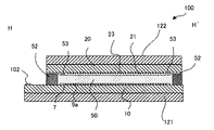
先ず、図2及び図3を参照して、液晶装置に設けられた液晶パネルの構成について説明する。ここに図2は、本実施形態に係る液晶パネルの全体構成を示す平面図であり、図3は、図2のH−H'線での断面図である。 First, the configuration of the liquid crystal panel provided in the liquid crystal device will be described with reference to FIGS. FIG. 2 is a plan view showing the entire configuration of the liquid crystal panel according to this embodiment, and FIG. 3 is a cross-sectional view taken along the line HH ′ of FIG.
図2及び図3において、本実施形態に係る液晶パネル100では、TFTアレイ基板10と対向基板20とが対向配置されている。TFTアレイ基板10と対向基板20との間に液晶層50が封入されており、TFTアレイ基板10と対向基板20とは、本発明に係る「画素領域」の一例としての画像表示領域10aの周囲に位置するシール領域に設けられたシール材52により相互に接着されている。シール材52は、両基板を貼り合わせるための、紫外線硬化樹脂からなり、製造プロセスにおいてTFTアレイ基板10上に塗布された後、紫外線照射により硬化させられたものである。また、シール材52中には、TFTアレイ基板10と対向基板20との間隔(基板間ギャップ)を所定値とするためのグラスファイバ或いはガラスビーズ等のギャップ材(図示せず)が散布されている。
2 and 3, in the
図2において、シール材52が配置されたシール領域の内側に並行して、画像表示領域10aの額縁領域を規定する遮光性の額縁遮光膜53が、対向基板20側に設けられている。周辺領域のうち、シール材52が配置されたシール領域の外側に位置する領域には、画像信号が供給される画像信号端子を含む外部回路接続端子102がTFTアレイ基板10の一辺に沿って設けられている。この一辺に沿ったシール領域よりも内側にサンプリング回路7が額縁遮光膜53に覆われるようにして設けられている。また、走査線駆動回路104は、この一辺に隣接する2辺に沿ったシール領域の内側に、額縁遮光膜53に覆われるようにして設けられている。また、TFTアレイ基板10上には、対向基板20の4つのコーナー部に対向する領域に、両基板間を上下導通材107で接続するための上下導通端子106が配置されている。これらにより、TFTアレイ基板10と対向基板20との間で電気的な導通をとることができる。
In FIG. 2, a light-shielding frame light-shielding
TFTアレイ基板10上には、外部回路接続端子102と、サンプリング回路7、走査線駆動回路104、上下導通端子106等とを電気的に接続するための引回配線90が形成されている。
On the
図3において、TFTアレイ基板10上には、駆動素子である画素スイッチング用TFTや走査線、データ線等の配線が作り込まれた積層構造が形成される。この積層構造の詳細な説明については図示を省略してあるが、画像表示領域10aには、画素スイッチング用TFTや走査線、データ線等の配線の上層に画素電極9aが設けられている。画素電極9aは典型的にはITO(Indium Tin Oxide)等の透明材料により、画素毎に所定のパターンで島状に形成される。
In FIG. 3, on the
画素電極9a上には、配向膜(図示せず)が形成されている。他方、対向基板20におけるTFTアレイ基板10との対向面上に、遮光膜23が形成されている。そして、遮光膜23上に、ITO等の透明材料からなる対向電極21が複数の画素電極9aと対向して形成されている。対向電極21上には配向膜(図示せず)が形成されている。また、液晶層50は、例えば一種又は数種類のネマティック液晶を混合した液晶からなり、これら一対の配向膜間で、所定の配向状態をとる。
An alignment film (not shown) is formed on the
液晶パネル100の駆動時において、画素毎に画素電極9aには画像信号が供給され、対向電極21との間で一定期間保持される。このようにして印加される電圧レベルにより液晶層50を構成する液晶は、分子集合の配向や秩序が変化することにより、光を変調し、階調表示を可能とする。ノーマリーホワイトモードであれば、各画素の単位で印加された電圧に応じて入射光に対する透過率が減少し、ノーマリーブラックモードであれば、各画素の単位で印加された電圧に応じて入射光に対する透過率が増加され、全体として画像表示領域10aにおいて画像信号に応じたコントラストをもつ光が出射する。尚、詳細な説明は省略するが、各画素はデータ線や走査線に画像信号等の各種信号が供給されることにより駆動され、画素電極9aは画素スイッチング用TFTによりスイッチング制御される。
When the
図3において、TFTアレイ基板10及び対向基板20の各々の液晶層50に対向しない側には、例えばガラス等の透明基板を用いて構成される防塵用基板121及び122が設けられている。この防塵用基板121及び122のデフォーカス作用により、TFTアレイ基板10及び対向基板20の各々の外側表面、即ち、防塵用基板121及び122と貼り合わせられる接着面に付着した埃や塵は、図1を参照して説明したようなスクリーン上の表示画面にピンボケの状態で表示されることとなる。よって、スクリーン上の表示画面に、前述したような埃や塵が明確に映りこむのを防止することができる。尚、液晶パネル100は防塵用基板121及び122のほか、図示は省略するが反射防止板等の光学要素が設けられるようにしてもよい。
In FIG. 3, dust-
ここでは図示しないが、TFTアレイ基板10上には、サンプリング回路7、走査線駆動回路104の他に、製造途中や出荷時の当該液晶装置の品質、欠陥等を検査するための検査回路、検査用パターン等が形成されていてもよい。
Although not shown here, on the
本実施形態に係る液晶装置は、以上に説明したような液晶パネル100が実装ケース内に収容されてなる。以下に液晶装置の構成について、図4から図15を参照して説明する。
The liquid crystal device according to the present embodiment includes the
図4は液晶装置を光入射側から見た平面図であり、図5は、液晶装置を光出射側から見た平面図である。また、図6は、液晶装置において実装ケースの側面側から見た側面図であり、図7は図6に示す液晶装置を、実装ケースの主要な構成要素ごとに分解した分解側面図である。 4 is a plan view of the liquid crystal device as viewed from the light incident side, and FIG. 5 is a plan view of the liquid crystal device as viewed from the light output side. FIG. 6 is a side view of the liquid crystal device as viewed from the side of the mounting case. FIG. 7 is an exploded side view of the liquid crystal device shown in FIG.
液晶装置において、液晶パネル100を収容する実装ケース600は、フレーム610、第1のフック620及び第2のフック630を含む。尚、第1のフック620は、本発明に係る「第1のカバー部材」の一例であり、第2のフック630は、本発明に係る「第2のカバー部材」の一例である。フレーム610は、例えば、ダイキャスティング(金型鋳造)により、アルミニウム等の金属から形成されている。第1のフック620及び第2のフック630は夫々、例えば、プレス加工により、アルミニウム、ステンレス等の金属から形成されている。
In the liquid crystal device, a mounting
図5から図7において、液晶パネル100にサンプリング回路7を介して各画素に画像信号を供給するためのデータ線駆動回路や画像信号供給回路等を含む、画像信号供給に係る回路部分は好ましくは駆動用IC(Integrated Circuit)チップ300内に内蔵される。或いは、画像信号供給に係る回路部分の一部が駆動用ICチップ300内に、それ以外の他部がTFTアレイ基板10上に内蔵されるようにしてもよい。
5 to 7, the circuit portion relating to the image signal supply including the data line driving circuit and the image signal supply circuit for supplying the
ここに、図8は、図4に示すA0−A0'線における液晶装置の断面部分の構成を示す断面図であり、図10は、図4に示すB0−B0'線における液晶装置の断面部分の構成を示す断面図である。 8 is a cross-sectional view showing a configuration of a cross-sectional portion of the liquid crystal device taken along line A0-A0 ′ shown in FIG. 4, and FIG. 10 is a cross-sectional portion of the liquid crystal device taken along line B0-B0 ′ shown in FIG. It is sectional drawing which shows this structure.
図8において、液晶パネル100は、外部回路接続端子102において配線基板200を介して駆動用ICチップ300に電気的に接続される。駆動用ICチップ300は例えばTAB(Tape Automated Bonding)技術により配線基板200に固着される。駆動用ICチップ300は、液晶パネル100に画像信号等を含む各種信号を供給するための各種回路が作り込まれている。即ち、図2及び図3を参照して説明した表示動作は、TFTアレイ基板10上の走査線駆動回路104やサンプリング回路7に加えて駆動用ICチップ300により液晶パネル100が駆動されることによりなされる。
In FIG. 8, the
実装ケース600における、フレーム610、第1のフック620及び第2のフック630の各々の構成についてより詳細に説明する。本実施形態では、図1を参照して説明したようなプロジェクタ1100において、第1のフック620の側から投射光が入射し、液晶パネル100の画像表示領域10aを透過した後、第2のフック630の側から出射されるということを前提とする。つまり、図1でいえば、ダイクロイックプリズム1112に対向するのは、第1のフック620ではなくて、第2のフック630ということになる。
Each configuration of the
図8又は図10に示すように、フレーム610を構成する部材は、液晶パネル100を収容するためくり抜かれたような状態となっており、これによる開口を開口部615が規定している。フレーム610内に液晶パネル100はその周縁部側から開口部615に包囲され、その開口内に収容される。
As shown in FIG. 8 or FIG. 10, the members constituting the
図11は、図10に示す液晶装置を、実装ケースの主要な構成要素ごとに分解した分解断面図である。図10において、前述したような蓋無き箱型の如き形状を有するフレーム610に対して、いわば蓋として機能し得る第1のフック620及び第2のフック630が装着される。即ち、フレーム610における開口部615により規定される開口は、第1のフック620及び第2のフック630が互いに反対側から装着されることにより閉じられた状態となる。
FIG. 11 is an exploded cross-sectional view of the liquid crystal device shown in FIG. 10 disassembled for each major component of the mounting case. In FIG. 10, a
第1のフック620は板状の部材であって、実装ケース600内において図4、図6及び図7、或いは図10に示すように液晶パネル100の一面に対向して開口部615を覆うようにフレーム610に対して装着される。この状態で、液晶パネル100は、第1のフック620に載置されるが如き状態でフレーム610内に収容される。
The
第1のフック620は、それを構成する部材が開口形状に形成された一部である、第1の窓625hを規定する第1の窓部625を有する。第1のフック620がフレーム610に装着された状態で、第1の窓部625は液晶パネル100と好ましくは相互に直接に当接する。第1の窓部625は、液晶パネル100の画像表示領域10aに対応して第1の窓625hを規定しており、図1に示すプロジェクタ1100において照射される投射光は第1の窓625hから液晶パネル100の画像表示領域10aに入射される。即ち第1の窓部625によって、液晶パネル100の画像表示領域10aの周辺に位置する周辺領域が当接される状態となる。液晶パネル100と第1の窓部625の辺縁とが相互に接触していることにより、前者から後者への熱の伝達が滞りなく行われるようになる。
The
第2のフック630は、図5、図6、図7或いは図10に示すように第1のフック620とは反対側から、液晶パネル100の他の面に対向して開口部615を覆うようにフレーム610に対して装着される。本実施形態では図11において、第2のフック630は、フレーム610に対して装着されることで弾力が生じるようなばね部分630aを有している。ばね部分630aは、例えば金属材料等からなる第2のフック630の一部を曲げることにより形成され、その曲げ形状に基づく弾力性を有する。
The
図11において、液晶装置の製造時に実装ケース600を組み立てる際には、例えば、第1のフック620をフレーム610に対して装着した後、液晶パネル100をフレーム610内に収容し開口部615に対してその周縁部側から接着材640により接着する。その後、第2のフック630をフレーム610に装着する。第2のフック630がフレーム610に対して装着されると、ばね部分630aに弾力が生じ、フレーム610内に収容された液晶パネル100には、第2のフック630が装着された側と反対側に向かって押される方向に力が加わる。従って、液晶パネル100をばね部分630aに生じる弾力により、第1のフック620に押し当ててフレーム610内に収容することが可能となる。従って、例えば既に説明したような特許文献1の構成と比較して、第1のフック620に対して液晶パネル100が顕著に離間されてフレーム610内に収容されるのをより有効に防止することができる。
In FIG. 11, when assembling the mounting
第2のフック630は、第1のフック620と同様に第2の窓635hを規定する第2の窓部635を有し、第2の窓部635において液晶パネル100と好ましくは相互に当接する。図1に示すプロジェクタ1100において、液晶パネル100の画像表示領域10aを透過した投射光は、第2のフック630において第2の窓635hから出射される。第2のフック630の側においても、第1のフック620と同様に液晶パネル100と第2の窓部635の辺縁とが相互に接触していることにより、前者から後者への熱の伝達が滞りなく行われるようになる。
Like the
ここに、図12には、本実施形態に対する比較例の液晶装置について、図10に対応する断面部分の構成を示す断面図である。尚、比較例については本実施形態と異なる構成にのみ着目して説明し、その他の構成については説明を省略する。 FIG. 12 is a cross-sectional view showing a configuration of a cross-sectional portion corresponding to FIG. 10 for a liquid crystal device of a comparative example with respect to the present embodiment. The comparative example will be described by paying attention only to the configuration different from the present embodiment, and description of other configurations will be omitted.
図12に示す比較例では、液晶パネル100の一面において周辺領域と当接する窓部715がフレーム610を構成する部材の一部により形成される。フレーム610に対してフック630が装着されることで、フレーム610における窓部715と対向する側は閉じられた状態となる。よって、比較例では図1に示すプロジェクタ1100において照射される投射光は窓部715によって規定される窓715hから液晶パネル100の画像表示領域10aに入射される。
In the comparative example shown in FIG. 12, a
この場合、フレーム610を構成する部材において窓部715の厚みd1のみを所定値まで薄くするのは製造上困難である。その結果、窓部715の表面と液晶パネル100の表面との間に生じる段差も大きくなるおそれがある。
In this case, it is difficult in manufacturing to reduce only the thickness d1 of the
これに対して、本実施形態では図10において、第1のフック620を構成する部材をフレーム610とは別個に調整することができる。例えば、液晶装置の製造時、第1のフック620を構成する部材に対してプレス加工を施すことにより、容易に当該部材の厚みを調整することが可能となる。これにより、容易に第1の窓部625の厚みd0も所定値まで薄くすることができる。具体的には例えば、図12において窓部715の厚みd1が0.4〜0.7mm程度であったのを、図10では第1の窓部625の厚みd0を0.1〜0.2mm程度まで薄くすることが可能となる。従って、実装ケース600の厚さが大きくなるのを防止して、液晶装置を小型化し、図1に示すプロジェクタ1100の小型化に寄与することができる。
On the other hand, in this embodiment, in FIG. 10, members constituting the
尚、第1のフック620は例えばステンレス等の金属材料により形成することで、より容易にプレス加工を施すことができ、更にはフレーム610の開口部615の表面より反射率を高くすることも可能となる。これにより、第1のフック620に液晶パネル100の周辺領域に向かって進行する光を反射して、液晶装置の顕著な温度上昇を抑制することができる。
The
ここに、図9は、図8に示す断面部分において、例えばプロジェクタ内で供給される冷却風の流れについて説明するための説明図である。図9において、冷却風の液晶装置に対する流れの一例を点線矢印により概略的に示してある。従って、実際の冷却風の流れは図9に示す点線矢印とは詳細には異なる場合もある。既に説明したように、プロジェクタ1100内においてシロッコファン等の手段によりライトバルブ1100R、1100G、又は1100Bを構成する液晶装置に対して冷却風が供給される。この冷却風は、概略的に実装ケース600の表面を図9中の点線矢印に沿って流れる。
FIG. 9 is an explanatory diagram for explaining the flow of cooling air supplied in the projector, for example, in the cross section shown in FIG. In FIG. 9, an example of the flow of cooling air to the liquid crystal device is schematically shown by dotted arrows. Therefore, the actual cooling air flow may differ in detail from the dotted arrow shown in FIG. As already described, cooling air is supplied to the liquid crystal devices constituting the light valves 1100R, 1100G, or 1100B by means such as a sirocco fan in the
本実施形態では、図10において、第1のフック620の第1の窓部625を所定値まで薄くすることで、第1の窓部625の厚みd0に起因してその表面と液晶パネル100の表面との間の段差が大きくなるのをより容易に防止することができる。加えて、実装ケース600内において、第1のフック620と液晶パネル100との間が離間することで、第1の窓部625の表面と液晶パネル100との間の段差が大きくなるのをより確実に防止することができる。従って、図9において、第1のフック620の側で、第1の窓625hから液晶パネル100の表面への流れ込みを効率良く行うことが可能となる。また、液晶パネル100を第1のフック620により確実に接触させることで、液晶パネル100から第1のフック620への熱伝導をより効率良く行うことも可能となる。更に、第1のフック620で、第1の窓部625及び液晶パネル100間の段差に起因して、第1の窓部625の縁に埃や塵等が溜まるのをより有効に防止することもできる。
In the present embodiment, in FIG. 10, the
本実施形態では、図10を参照して説明したように、第1の窓部625の厚みd0を容易に所定値とするために、第1のフック620を構成する部材の厚みを薄くしたり、またプレス加工を施しやすい材料により形成することで、第1のフック620における強度が小さくなるおそれがある。その結果、第1のフック620に比較的強い力が加わることにより、第1のフック620の歪みや、実装ケース600内に収容された液晶パネル100に第1のフック620を介して力が加わることによる破損等の弊害が生じ得る。このような弊害を防止するために、本実施形態の実装ケース600の各部は好ましくは以下のような特徴的な構成を有する。
In the present embodiment, as described with reference to FIG. 10, in order to easily set the thickness d0 of the
図4において、フレーム610においては突起部613が、フレーム610の取り付け穴616に対応する4箇所に対して設けられる。尚、取り付け穴616はフレーム610を構成する部材により規定されており、図1に示すプロジェクタ1100内に液晶装置をライトバルブ1100R、1100G又は1100Bとして取り付ける際に利用される。
In FIG. 4,
図4、図6又は図7に示すように、突起部613は第1のフック620が装着される側に設けられ、図6によく示されるように第1のフック620の表面から突出するような高さで形成される。実装ケース600において、フレーム610に第1のフック620が装着された状態で、第1のフック620の側を設置面とする場合(即ち図6中、突起部613が設けられた側を上側にして実装ケース600を設置する構成を示してあるが、これと反対側に、突起部613が設けられた側を下側にして実装ケース600を設置する場合)、第1のフック620の表面より突出する突起部613により当該設置により生じる力を受けることができる。従って、このような設置により第1のフック620、及び第1のフック620を介してフレーム610内に収容された液晶パネル100に比較的強い力が加わることにより、破損等が生じる事態を回避することが可能となる。
As shown in FIG. 4, FIG. 6, or FIG. 7, the
或いは、図11を参照して説明したように液晶装置の製造時に実装ケース600を組み立てる場合、フレーム610に第1のフック620が装着された状態で、第1のフック620の側を設置面として(即ち図6中、突起部613が設けられた側を下側にして設置する場合)、液晶パネル100を実装し且つ第2のフック630をフレーム610に装着させる各工程を行う場合においても、各工程で、上述のように突起部613で力を受けることにより第1のフック620に加わる力を緩和することができる。その結果、製造プロセスの歩留まりを向上させることが可能となる。
Alternatively, when the mounting
本実施形態では、図4において4箇所に配置された突起部613は夫々、放熱用のフィン及び導風板の少なくとも一方を兼ねるように形成されてもよい。或いは、図4に示す構成に限定されず、例えば4箇所のうち3箇所に突起部613を設け、そのうち1箇所には放熱用のフィン或いは導風板を設けるようにしてもよい。突起部613が放熱用のフィン及び導風板の少なくとも一方を兼ねるように構成すれば、突起部613と放熱用のフィン及び導風板とを夫々別個に設ける場合と比較して、これらに要するフレーム610における配置面積を小さくして、フレーム610を容易に小型化することが可能となる。従って、実装ケース600も小型化することが可能となり、液晶装置の小型化に寄与することができる。尚、放熱用のフィンを設けることにより、図9においてフレーム610の冷却風と接触する表面の面積が増加すると共に冷却風を効率良く流すことが可能となる。また、導風板を設ける場合には、図9の冷却風の流れにおける風上側、即ち同図中では右から左へ冷却風が流れるようすを示してあるが、この場合には右側に対して設けることで、第1の窓625hから液晶パネル100の表面に対して効率良く冷却風が流れ込むようにすることができる。従って、放熱用のフィンや導風板を設けることでフレーム610からの放熱を効率良く行うことができる。
In the present embodiment, the
ここに、図4、図6、図8等に示すようにフレーム610において、第1のフック620が装着される側に、それを構成する部材の一部が配線基板200に沿って延在されてなる放熱部611が設けられている。図6又は図8において、放熱部611は配線基板200上の駆動用ICチップ300からの熱の伝導が可能なように設けられている。その結果、駆動用ICチップ300からの熱を放熱部611において、効率良く液晶装置外に放散させることが可能となる。
Here, as shown in FIGS. 4, 6, 8, etc., in the
図4、図6、或いは図8に示すように第1のフック620は、それを構成する部材の縁部が折り曲げられてなる折り曲げ部621を有している。ここに、図13は、図4における点線A1で囲まれた部分を拡大して示す拡大概略図であり、図15は、図8における点線A2で囲まれた部分を拡大して示す拡大概略図である。図15によく示されるように、折り曲げ部621は、第1のフック620がフレーム610に装着された状態で当接する開口部615の表面形状に沿うように折り曲げられている。よって、第1のフック620と開口部615の壁部分とを隙間無く合わせることができる。従って、このような隙間が生じるために、第1のフック620に対して液晶パネル100が離間するのを防止することが可能となる。よって、第1のフック620の第1の窓部625の表面と液晶パネル100との間の段差が大きくなるのを防止して、第1の窓625hから液晶パネル100への冷却風の流れ込みを効率良くすることができる。
As shown in FIG. 4, FIG. 6, or FIG. 8, the
また、第1のフック620の部材の厚みを、第1の窓部625の厚みを調整するために薄くした結果、強度が劣化した場合に、実装ケース600内で第2のフック630からの弾力により液晶パネル100が押し当てられて、第1のフック620に対して力が加わり、第1のフック620に歪みが生じるおそれがある。折り曲げ部621によって第1のフック620をフレーム610の開口部615の壁部分に隙間無く合わせてフレーム610に対して押さえて装着することで、加わった力により第1のフック620に歪みが生じるのをより有効に防止することができる。
Further, when the thickness of the member of the
図4又は図13において、折り曲げ部621は、これを部分的に切り欠いて形成された凹部622を有する。ここに、図14は、第1のフックが順送型の製造装置を用いて製造されることについて説明するための説明図である。図14に示すように、順送型の製造装置を用いて第1のフック620を量産する場合に、折り曲げ部621の一部に凹部622を設けることにより、多数の第1のフック620を凹部622において相互に繋げて連続させ、容易に製造することが可能となる。
In FIG. 4 or FIG. 13, the
図4又は図13において、フレーム610には凹部622に対応して突起部613が設けられる。第1のフック620において折り曲げ部621が欠けた凹部622で、例えば第2のフック630からの弾力により液晶パネル100が押し当てられるために加わる力に対して強度が劣化するおそれがある。凹部622に対応させて突起部613を配置することで、凹部622における強度を補強することができる。従って、第2のフック630からの弾力により液晶パネル100が押し当てられて加わる力により、凹部622において第1のフック620の歪みが生じるのを防止することができる。また、図13に示すように凹部622の中にまで入り込んで突起部613を形成することができるので、その配置面積をより大きく確保することが可能である。尚、フレーム610において、上述したような凹部622に対する補強を行うための部材を突起部613と別個に設ける場合と比較して、これらに要するフレーム610における配置面積を小さくして、フレーム610を容易に小型化することが可能となる。凹部622に対する補強を行う構成として、凹部622に対応させて突起部613に代えて若しくは加えて、導風板又は放熱用のフィンが配置されるようにしてもよい。
4 or 13, the
図4又は図13において、第1のフック620には折り曲げ部621に沿って溝部623が形成される。図15において、溝部623は、典型的にはハーフパンチ加工により第1のフック620の部材の厚みの半分程度を抜くことにより形成される。よって、溝部623の底部は第1のフック620における、フレーム610の開口部615と対向する側の表面から突出するように形成される。従って、溝部623を開口部615の縁に合わせて配置し、これに沿う折り曲げ部621のストッパーとして機能させることが可能となる。よって、折り曲げ部621とフレームの開口部615とで位置ずれが生じるのを防止して、より確実に第1のフック620と開口部615の壁部分とを隙間無く合わせることができる。従って、より確実に、第2のフック630からの弾力により液晶パネル100が押し当てられて加わる力により、第1のフック620に歪みが生じるのを防止することができる。
In FIG. 4 or FIG. 13, a
図6、図7、図10及び図11を参照して、第1のフック620をフレーム610に装着させるための構成について説明する。図6又は図7において、第1のフック620は、それを構成する部材の一部を、図10又は図11に示すようにフレーム610の側面側に折り曲げてなる装着部628を有すると共に、フレーム610は爪部619を有する。第1のフック620は、装着部628を爪部619に掛けることによりフレーム610に対して装着される。装着部628がフレーム610の側面においてその壁部分に接触することにより、第1のフック620からフレーム610への熱伝導が可能となっている。尚、第2のフック630も好ましくは、第1のフック620と同様に爪部619においてフレーム610に対して装着される。
A configuration for attaching the
第1のフック620において、フレームに610装着された状態では爪部619に掛けられた装着部628により引っ張られるような力が生じ、歪みが生じるおそれがある。装着部628は引っ掛け部626を有し、フレーム610の爪部619が設けられた壁部分には、引っ掛け部626に対応する止め部617が形成されている。引っ掛け部626は、装着部628が爪部619に装着された状態で、装着部628が爪部619により引っ張られる力により止め部617に引っ掛かって止められる。これにより、引っ掛け部626により装着部628が引っ張られる力を緩和することが可能となる。従って、装着部628が爪部619に装着されることで第1のフック620に歪みが生じるのを防止することができる。
In the state where the
次に、図16及び図17を参照して、本実施形態において特徴的な実装ケースの入射側表面部分に係る構成について説明する。図16は、図4において第1及び第2の遮光膜と、第1の窓部との配置関係を示す平面図であり、図17は、図10に示す断面部分について、液晶装置における光の反射の概要を説明するための断面図である。尚、図17では図10における接着材640については図示を省略してある。 Next, with reference to FIG. 16 and FIG. 17, a configuration related to the incident-side surface portion of the mounting case characteristic in the present embodiment will be described. 16 is a plan view showing the positional relationship between the first and second light-shielding films and the first window portion in FIG. 4, and FIG. 17 is a cross-sectional view of FIG. It is sectional drawing for demonstrating the outline | summary of reflection. In FIG. 17, the illustration of the adhesive 640 in FIG. 10 is omitted.
図2又は図3を参照して説明したように、液晶パネル100において額縁遮光膜53が、本発明に係る「第1の遮光膜」の一例として画像表示領域10aの周縁に設けられる。尚、額縁遮光膜53は図3を参照して説明したように対向基板20側に設けられる構成に限定されず、一部又は全部がTFTアレイ基板10側に内蔵遮光膜として設けられてもよい。以下では、額縁遮光膜53を「第1の遮光膜」として説明する。図1においてプロジェクタ1100によってスクリーン等に表示される有効画面の領域は、第1の遮光膜53によって規定される。
As described with reference to FIG. 2 or FIG. 3, in the
図16又は図17において、対向基板20の側に配置された、本発明に係る「他の基板」の一例としての防塵用基板122には、第1の遮光膜53に対応して額縁状のパターンで第2の遮光膜55が形成される。尚、第2の遮光膜55は、液晶パネル100を、例えば図17に示す構成とは反対側即ちTFTアレイ基板10の側を光入射側に配置する場合には、TFTアレイ基板10の側に配置された防塵用基板121(図3参照)に設けるようにしてもよい。
In FIG. 16 or 17, the
ここに、図17において点線矢印は図1に示すプロジェクタ1100の投射光について、液晶装置に対する進路の一例を概略的に示している。図1に示すプロジェクタ1100における投射光のうち、液晶パネル100の画像表示領域10a外の周辺領域に向かって進行する光は、第1の遮光膜55及び第2の遮光膜53により反射されて遮光される。また、液晶パネル100の画像表示領域10a外の周辺領域に向かって進行する光は、実装ケース600の光入射側において、第1のフック620及びフレーム610の表面部分においても反射されて遮光される。
Here, in FIG. 17, a dotted arrow schematically shows an example of a path for the liquid crystal device with respect to the projection light of the
本実施形態では、フレーム610及び第1のフック620のうち少なくとも一方において、その光入射側に面する表面部分は少なくとも部分的に、第1の遮光膜53及び第2の遮光膜55よりも光の反射率の低い材料により形成される。例えば、第1の遮光膜53及び第2の遮光膜55は夫々、クロム(Cr)により光の反射率が50〜60%程度となるように形成されるか、或いはアルミニウム(Al)により光の反射率が85%以上となるように形成される。これに対して、第1のフック620はステンレスにより、光入射側の表面部分が少なくとも部分的に光の反射率が30〜50%程度となるように形成される。第1のフック620に加えて若しくは代えてフレーム610は例えば、アルミニウム(Al)又はマグネシウム(Mg)により形成され、且つ防錆処理等が施されることにより、光入射側に面する表面部分が少なくとも部分的に、光の反射率が20%以下となるように形成される。
In the present embodiment, in at least one of the
従って、実装ケース600の光入射側の表面部分において、フレーム610及び第1のフック620のうち少なくとも一方の表面部分は少なくとも部分的に、第1の遮光膜53及び第2の遮光膜55よりも光が反射され難いように形成することができる。よって、実装ケース600の光入射側の表面部分において、画像表示領域10a外の周辺に向かって進行し表示に寄与しない光の反射を抑制することができる。従って、図17中の点線矢印で示されるように、実装ケース600の光入射側において例えば第1のフック620の表面部分で反射した光が、液晶装置外においてその光入射側に配置された部材、例えば同図中の偏光板等の光学部材やその支持部材2002により再反射されて迷光が生じるのを抑制することができる。その結果、多量の迷光が画像表示領域10aから出射される表示光に紛れ込む事態をより有効に防止することが可能となる。
Accordingly, in the surface portion on the light incident side of the mounting
図1に示すプロジェクタ1100において投射光は、液晶装置に対して画像表示領域10aの中央に向かうほど光量が多くなるようにしぼりがかけられた強力な光で投射される。即ちこの場合、液晶装置においては、画像表示領域10aの中央に向かうほど光量が多くなるような光が入射される。よって、画像表示領域10aの縁付近では画像表示領域10a外よりも液晶装置に入射される光の光量は多くなる。従って、上述したように実装ケース600の光入射側で、フレーム610や第1のフック620の表面部分の反射率を低くすると、画像表示領域10aの縁付近に進行する強力な光に対する液晶装置における遮光性能が劣化するおそれがある。
In the
本実施形態では、第1の遮光膜53及び第2の遮光膜55の光の反射率が比較的高くなるように形成することで、実装ケース600の光入射側の表面部分の反射率を低くするためにその遮光性能が劣化しても、画像表示領域10aの縁付近に進行する強力な光を第1の遮光膜53及び第2の遮光膜55で反射してより確実に遮光することができる。従って、画像表示領域10aの縁付近に進行する強力な光が入射されることで液晶パネル100内の温度が顕著に上昇し、そのために液晶装置の表示品質が劣化するのをより確実に防止することができる。
In the present embodiment, the first
図16によく示されるように、第2の遮光膜55は、防塵用基板122上において第1の遮光膜53よりも画像表示領域10aに対して部分的に外周側に位置するように形成される。図17において第2の遮光膜55は、一部において第1の遮光膜53に対して重なりつつ、他部において第1の遮光膜53よりも画像表示領域10aに対して外周側に配置される。よって、液晶パネル100に対して画像表示領域10a外に向かって進行する光について、第1の遮光膜53及び第2の遮光膜55により、互いに重なる部分で光漏れが生じるのを防止しつつより広い領域で遮光することが可能となる。従って、画像表示領域10aの縁付近に進行する強力な光を第1の遮光膜53及び第2の遮光膜55でより確実に遮光することができる。
As well shown in FIG. 16, the second
また、図16において第1のフック620の第1の窓部625は、第1の遮光膜53及び第2の遮光膜55よりも画像表示領域10aに対して部分的に外周側に位置するように形成される。言い換えれば、第1の窓部625よりも第1の遮光膜53及び第2の遮光膜55の各々は部分的にそれよりも内側に配置される。第1の窓部625の光入射側の表面部分は、上述したように第1の遮光膜53及び第2の遮光膜55よりも光の反射率の低い材料により形成されるのが好ましい。よって、このように光の反射性能が低下した第1の窓部625とは重ならない第1の遮光膜53及び第2の遮光膜55の各々の部分で、画像表示領域10aの縁付近に進行する光を反射させることで、より確実に遮光することができる。
In FIG. 16, the
図17において点線矢印で示されるように、このように画像表示領域10aの縁付近に進行する光を第1の遮光膜53及び第2の遮光膜55で反射することで、投射光等の液晶装置外から画像表示領域10aに対して進行する光の進路に近似しつつ、光源側に逆行する方向に進行させることが可能となる。従って、画像表示領域10aの縁付近に進行する光が第1の遮光膜53及び第2の遮光膜55で反射されることに起因する迷光の発生を抑制することができる。
As indicated by the dotted arrow in FIG. 17, the light traveling in the vicinity of the edge of the
また、一方で図17において、第1の窓部625を第1の遮光膜53及び第2の遮光膜55の各々と部分的に重なるように配置することで、液晶パネル100に対して画像表示領域10a外に向かって進行する光について、第1の窓部625に加えて第1の遮光膜53及び第2の遮光膜55により、互いに重なる部分で光漏れが生じるのを防止しつつより広い領域で遮光することが可能となる。
On the other hand, in FIG. 17, the
ここに既に説明したように、画像表示領域10aの中央に向かうほど光量が多くなるようにしぼりがかけられた強力な光で投射される投射光等について、第1の遮光膜53及び第2の遮光膜55の各々の部分で、画像表示領域10aの縁付近に進行する強力な光が反射され、それよりも画像表示領域10aの外側に向かって進行し光量がより少ない光が第1の窓部625で反射される。従って、液晶パネル100内の温度上昇を抑制しつつ、実装ケース600における光の反射に起因する迷光の発生をより確実に抑制することが可能となる。
As already described herein, with respect to the projection light and the like projected with powerful light that has been reduced so that the amount of light increases toward the center of the
本実施形態では、第1のフック620において光の反射率はフレーム610とは別個に調整することができる。従って、光の反射率を調整することで第1のフック620では、フレーム610と別個に光を反射され易く調整したり、またその逆の調整も容易に行うことができる。第1のフック620の光入射側の表面部分は、フレーム610よりもより広く面するため、少なくとも部分的にフレーム610よりは光の反射率が高くなるように形成するのが好ましい。例えば、既に説明したように、第1のフック620は光入射側の表面部分が少なくとも部分的に光の反射率が30〜50%程度となるように形成され、フレーム610は光入射側に面する表面部分が少なくとも部分的に、光の反射率が20%以下となるように形成される。これにより、実装ケース600において光入射側の表面部分では、より広く液晶装置の光の入射される側に面する第1のフック620において、画像表示領域10a外の周辺に向かって進行し表示に寄与しない光をより多く反射させることができる。従って、液晶パネル100に対してより多くの光が入射されることによる、液晶パネル100内の温度上昇をより有効に抑制することが可能となる。
In the present embodiment, the light reflectance of the
従って、以上説明したような本実施形態では、液晶装置における冷却効率をより確実に向上させつつ、高品質な表示を行うことが可能となる。 Therefore, in the present embodiment as described above, it is possible to perform high-quality display while improving the cooling efficiency in the liquid crystal device more reliably.
<第2実施形態>
次に、本発明の電気光学装置に係る第2実施形態について説明する。第2実施形態については、第1実施形態と異なる点についてのみ、図18を参照して説明する。図18は、図17に対応する断面部分について、第2実施形態の液晶装置における光の反射の概要をその構成と併せて説明するための断面図である。尚、図18においては図17と同様に、点線矢印によって図1に示すプロジェクタ1100の投射光について、液晶装置に対する進路の一例を概略的に示している。
Second Embodiment
Next, a second embodiment according to the electro-optical device of the invention will be described. In the second embodiment, only differences from the first embodiment will be described with reference to FIG. FIG. 18 is a cross-sectional view for explaining an outline of light reflection in the liquid crystal device according to the second embodiment together with the configuration of the cross-sectional portion corresponding to FIG. In FIG. 18, similarly to FIG. 17, an example of a path with respect to the liquid crystal device is schematically shown with respect to the projection light of the
第2実施形態に係る液晶装置は、既に図12を参照して説明した比較例と同様の構成を有しており、液晶パネル100の一面において周辺領域と当接する窓部715がフレーム610を構成する部材の一部により形成され、フレーム610に対してフック630が装着される。また、窓部715によって規定される窓715hから液晶パネル100の画像表示領域10aに光が入射可能となっている。
The liquid crystal device according to the second embodiment has a configuration similar to that of the comparative example already described with reference to FIG. 12, and a
図18中の点線矢印により示されるように、図1に示すプロジェクタ1100における投射光のうち、液晶パネル100の画像表示領域10a外の周辺領域に向かって進行する光は、第1の遮光膜55及び第2の遮光膜53により反射されると共に、実装ケース600の光入射側においてフレーム610の表面部分においても反射されて遮光される。
As indicated by the dotted arrows in FIG. 18, the light traveling toward the peripheral region outside the
フレーム610において、光入射側の表面部分は少なくとも部分的に第1の遮光膜53及び第2の遮光膜55よりも光の反射率の低い材料により形成される。例えば、第1の遮光膜53及び第2の遮光膜55は夫々光の反射率が40%以上となるように形成され、フレーム610の光入射側の表面部分は少なくとも部分的に光の反射率が30%以下となるように形成される。従って、実装ケース600の光入射側の表面部分において、フレーム610の表面部分が少なくとも部分的に第1の遮光膜53及び第2の遮光膜55よりも光が反射され難いように形成することができる。従って、第2実施形態においても第1実施形態と同様に、実装ケース600の光入射側の表面部分で反射する光に起因する迷光の発生を抑制することが可能となる。
In the
また、フレーム610の窓部715は、第1の遮光膜53及び第2の遮光膜55よりも画像表示領域10aに対して部分的に外周側に位置するように形成される。言い換えれば、窓部715よりも第1の遮光膜53及び第2の遮光膜55の各々は部分的にそれよりも内側に配置される。窓部715の光入射側の表面部分は、上述したように第1の遮光膜53及び第2の遮光膜55よりも光の反射率の低い材料により形成されるのが好ましい。よって、このように光の反射性能が低下した窓部715とは重ならない第1の遮光膜53及び第2の遮光膜55の各々の部分で、画像表示領域10aの縁付近に進行する光を反射させることで、このような反射による迷光の発生を抑制しつつより確実に遮光することができる。
Further, the
また、一方で窓部715を第1の遮光膜53及び第2の遮光膜55の各々と部分的に重なるように配置することで、液晶パネル100に対して画像表示領域10a外に向かって進行する光について、窓部715に加えて第1の遮光膜53及び第2の遮光膜55により、互いに重なる部分で光漏れが生じるのを防止しつつより広い領域で遮光することが可能となる。
On the other hand, the
ここに、画像表示領域10aの中央に向かうほど光量が多くなるようにしぼりがかけられた強力な光で投射される投射光等について、第1の遮光膜53及び第2の遮光膜55の各々の部分で、画像表示領域10aの縁付近に進行する強力な光が反射され、それよりも画像表示領域10aの外側に向かって進行し光量がより少ない光が窓部715で反射される。従って、液晶パネル100内の温度上昇を抑制しつつ、実装ケース600における光の反射に起因する迷光の発生をより確実に抑制することが可能となる。
Here, each of the first light-shielding
従って、以上説明したような第2実施形態では、第1実施形態と同様の効果を得ることが可能となる。 Therefore, in the second embodiment as described above, it is possible to obtain the same effect as in the first embodiment.
本発明は上述の実施形態で説明した液晶装置以外にも、シリコン基板上に素子を形成する反射型液晶装置(LCOS)、プラズマディスプレイ(PDP)、電解放出型ディスプレイ(FED、SED)、有機ELディスプレイ、デジタルマイクロミラーデバイス(DMD)、電気泳動装置等にも適用可能である。 In addition to the liquid crystal devices described in the above embodiments, the present invention is not limited to a reflective liquid crystal device (LCOS), a plasma display (PDP), a field emission display (FED, SED), or an organic EL device. The present invention can also be applied to a display, a digital micromirror device (DMD), an electrophoresis apparatus, and the like.
本発明は、上述した実施形態に限られるものではなく、請求の範囲及び明細書全体から読み取れる発明の要旨或いは思想に反しない範囲で適宜変更可能であり、そのような変更を伴う電気光学装置及び電子機器もまた本発明の技術的範囲に含まれるものである。 The present invention is not limited to the above-described embodiments, and can be appropriately changed without departing from the spirit or concept of the invention that can be read from the claims and the entire specification. Electronic devices are also included in the technical scope of the present invention.
10a…画像表示領域、20…対向基板、53…額縁遮光膜(第1の遮光膜)、55…第2の遮光膜、100…液晶パネル、121、122…防塵用基板、600…実装ケース、610…フレーム、615…開口部、620…第1のフック、625h…第1の窓、630…第2のフック、635h…第2の窓、630a…ばね部分、625…第1の窓部、635…第2の窓部、715…窓部、715h…窓
DESCRIPTION OF
Claims (7)
前記電気光学パネルを収容するフレームと、該フレームの前記光入射側に装着され、前記画素領域に対応して設けられた窓部を有し、前記第2の遮光膜と重なるように設けられたカバー部材とを有する実装ケースと
を備え、
前記カバー部材の少なくとも光入射側の面は、前記第1及び第2の遮光膜よりも光の反射率の低い材料により形成されると共に、前記フレームよりも光の反射率の高い材料により形成されていることを特徴とする電気光学装置。 A pair of substrates sandwiching the electro-optic material, another substrate provided on the opposite side of the electro-optic material of at least one of the pair of substrates, and provided on at least one substrate of the pair of substrates A first light-shielding film formed in a frame shape at the periphery of a pixel region in which a plurality of pixels are arranged, and a frame shape formed on the other substrate along the outer periphery of the first light-shielding film An electro-optical panel having a second light-shielding film;
A frame that accommodates the electro-optical panel, and a window portion that is attached to the light incident side of the frame and is provided corresponding to the pixel region, and is provided so as to overlap the second light shielding film. A mounting case having a cover member ,
At least the light incident side surface of said cover member, said first and second light shielding film is formed by a material having a low light reflectivity than Rutotomoni is formed by a material having high light reflectivity than the frame electro-optical device characterized in that is.
前記折り曲げ部は、前記突起部に対応して設けられた凹部を有することを特徴とする請求項2に記載の電気光学装置。The electro-optical device according to claim 2, wherein the bent portion has a concave portion provided corresponding to the protruding portion.
Priority Applications (1)
| Application Number | Priority Date | Filing Date | Title |
|---|---|---|---|
| JP2008263143A JP5332482B2 (en) | 2008-10-09 | 2008-10-09 | Electro-optical device and electronic apparatus |
Applications Claiming Priority (1)
| Application Number | Priority Date | Filing Date | Title |
|---|---|---|---|
| JP2008263143A JP5332482B2 (en) | 2008-10-09 | 2008-10-09 | Electro-optical device and electronic apparatus |
Publications (3)
| Publication Number | Publication Date |
|---|---|
| JP2010091877A JP2010091877A (en) | 2010-04-22 |
| JP2010091877A5 JP2010091877A5 (en) | 2011-11-24 |
| JP5332482B2 true JP5332482B2 (en) | 2013-11-06 |
Family
ID=42254645
Family Applications (1)
| Application Number | Title | Priority Date | Filing Date |
|---|---|---|---|
| JP2008263143A Expired - Fee Related JP5332482B2 (en) | 2008-10-09 | 2008-10-09 | Electro-optical device and electronic apparatus |
Country Status (1)
| Country | Link |
|---|---|
| JP (1) | JP5332482B2 (en) |
Family Cites Families (3)
| Publication number | Priority date | Publication date | Assignee | Title |
|---|---|---|---|---|
| JP3697104B2 (en) * | 1999-03-30 | 2005-09-21 | セイコーエプソン株式会社 | Liquid crystal device and projection display device having the same |
| JP2003029243A (en) * | 2001-07-19 | 2003-01-29 | Seiko Epson Corp | Display device and projector using the same |
| JP4016639B2 (en) * | 2001-10-31 | 2007-12-05 | セイコーエプソン株式会社 | Electro-optical device, manufacturing method thereof, and projection display device |
-
2008
- 2008-10-09 JP JP2008263143A patent/JP5332482B2/en not_active Expired - Fee Related
Also Published As
| Publication number | Publication date |
|---|---|
| JP2010091877A (en) | 2010-04-22 |
Similar Documents
| Publication | Publication Date | Title |
|---|---|---|
| JP5504557B2 (en) | Electro-optical device, mounting case for electro-optical device, and electronic apparatus | |
| JP5533001B2 (en) | Electro-optical device and electronic apparatus | |
| JP5515813B2 (en) | Electro-optical device and electronic apparatus | |
| JP5672718B2 (en) | Electro-optical device and electronic apparatus | |
| JP5470800B2 (en) | Electro-optical device and electronic apparatus | |
| JP5287119B2 (en) | Electro-optical device and electronic apparatus | |
| JP5109713B2 (en) | Electro-optical device and electronic apparatus | |
| JP2009204958A (en) | Electro-optic device and method for manufacturing the same, and electronic apparatus | |
| JP2007279626A (en) | Electro-optical device and electronic apparatus provided with the same | |
| JP5332482B2 (en) | Electro-optical device and electronic apparatus | |
| JP2010256662A (en) | Electro-optical device and electronic apparatus | |
| JP2008096615A (en) | Electro-optical device and electronic equipment having the same | |
| JP2009122309A (en) | Manufacturing method of electrooptical device, electrooptical device, and electronic device | |
| JP6269749B2 (en) | Electro-optical device and electronic apparatus | |
| JP2008153915A (en) | Electrooptical device module and electronic device | |
| JP5994907B2 (en) | Electro-optical device and electronic apparatus | |
| JP5834402B2 (en) | Electro-optical device and electronic apparatus | |
| JP5370168B2 (en) | Electro-optical device and electronic apparatus | |
| JP2009128665A (en) | Electro-optical device and electronic equipment | |
| JP2010256667A (en) | Electro-optical device and electronic equipment | |
| JP2009058567A (en) | Electro-optical device and method for manufacturing the same, and electronic apparatus | |
| JP2010060968A (en) | Electro-optical device and electronic apparatus | |
| JP2009198542A (en) | Electrooptical apparatus and electronic equipment | |
| JP2010113187A (en) | Electro-optical device and electronic equipment | |
| JP2011145445A (en) | Electro-optical device and electronic apparatus |
Legal Events
| Date | Code | Title | Description |
|---|---|---|---|
| A521 | Written amendment |
Free format text: JAPANESE INTERMEDIATE CODE: A523 Effective date: 20111005 |
|
| A621 | Written request for application examination |
Free format text: JAPANESE INTERMEDIATE CODE: A621 Effective date: 20111005 |
|
| RD01 | Notification of change of attorney |
Free format text: JAPANESE INTERMEDIATE CODE: A7421 Effective date: 20120327 |
|
| A977 | Report on retrieval |
Free format text: JAPANESE INTERMEDIATE CODE: A971007 Effective date: 20121226 |
|
| A131 | Notification of reasons for refusal |
Free format text: JAPANESE INTERMEDIATE CODE: A131 Effective date: 20130115 |
|
| A521 | Written amendment |
Free format text: JAPANESE INTERMEDIATE CODE: A523 Effective date: 20130228 |
|
| TRDD | Decision of grant or rejection written | ||
| A01 | Written decision to grant a patent or to grant a registration (utility model) |
Free format text: JAPANESE INTERMEDIATE CODE: A01 Effective date: 20130702 |
|
| A61 | First payment of annual fees (during grant procedure) |
Free format text: JAPANESE INTERMEDIATE CODE: A61 Effective date: 20130715 |
|
| R150 | Certificate of patent or registration of utility model |
Ref document number: 5332482 Country of ref document: JP Free format text: JAPANESE INTERMEDIATE CODE: R150 Free format text: JAPANESE INTERMEDIATE CODE: R150 |
|
| S531 | Written request for registration of change of domicile |
Free format text: JAPANESE INTERMEDIATE CODE: R313531 |
|
| R350 | Written notification of registration of transfer |
Free format text: JAPANESE INTERMEDIATE CODE: R350 |
|
| LAPS | Cancellation because of no payment of annual fees |