JP5370168B2 - Electro-optical device and electronic apparatus - Google Patents
Electro-optical device and electronic apparatus Download PDFInfo
- Publication number
- JP5370168B2 JP5370168B2 JP2010005657A JP2010005657A JP5370168B2 JP 5370168 B2 JP5370168 B2 JP 5370168B2 JP 2010005657 A JP2010005657 A JP 2010005657A JP 2010005657 A JP2010005657 A JP 2010005657A JP 5370168 B2 JP5370168 B2 JP 5370168B2
- Authority
- JP
- Japan
- Prior art keywords
- electro
- liquid crystal
- cooling air
- opening
- optical
- Prior art date
- Legal status (The legal status is an assumption and is not a legal conclusion. Google has not performed a legal analysis and makes no representation as to the accuracy of the status listed.)
- Expired - Fee Related
Links
Images


Landscapes
- Projection Apparatus (AREA)
- Devices For Indicating Variable Information By Combining Individual Elements (AREA)
- Liquid Crystal (AREA)
Abstract
Description
本発明は、例えば液晶表示装置等の電気光学装置、及び該電気光学装置を備えた、例えば液晶プロジェクター等の電子機器の技術分野に関する。 The present invention relates to a technical field of an electro-optical device such as a liquid crystal display device and an electronic apparatus such as a liquid crystal projector provided with the electro-optical device.
この種の電気光学装置として、例えば液晶パネル等の電気光学パネルを実装ケースに収容することで構成されるものがある。このような電気光学装置では、例えば光源から発せられた光を電気光学パネルの表示面に入射させることで、スクリーン等に画像が表示される。この際、光源から発せられる光は比較的強い光である場合が多く、電気光学パネルは、光が投射されることで光の持つエネルギーを吸収して発熱してしまう。 As this type of electro-optical device, for example, there is one configured by housing an electro-optical panel such as a liquid crystal panel in a mounting case. In such an electro-optical device, for example, an image is displayed on a screen or the like by causing light emitted from a light source to enter the display surface of the electro-optical panel. At this time, the light emitted from the light source is often relatively strong light, and the electro-optical panel absorbs the energy of the light and generates heat when the light is projected.
装置における過度な発熱は不具合や故障の原因となるおそれがあるため、上述したような電気光学装置には、温度上昇を低減する冷却機構や放熱機構が設けられる場合がある。例えば特許文献1では、電気光学装置に冷却風を導入すると共に、実装ケースの一部を盛り上がるように形成することで、効果的な冷却を実現しようとする技術が開示されている。
Since excessive heat generation in the apparatus may cause a malfunction or failure, the electro-optical apparatus as described above may be provided with a cooling mechanism or a heat dissipation mechanism that reduces a temperature rise. For example,
しかしながら、上述した技術のように冷却風を用いて装置を冷却する場合には、装置の風上側と風下側とで冷却効率が異なることに起因して、電気光学パネルに温度ムラが生じてしまうことがある。具体的には、冷却風の当たりがよい風上側は比較的効率よく冷却されるのに対し、冷却風の当たりが悪い風下側は冷却効率が悪くなるため、風上側と比べて風下側の温度が高くなってしまう。このように、上述した技術には、装置全体を均一に冷却することが困難であるという技術的問題点がある。 However, when the apparatus is cooled using cooling air as in the above-described technique, temperature unevenness occurs in the electro-optical panel due to the difference in cooling efficiency between the windward side and the leeward side of the apparatus. Sometimes. Specifically, the leeward side where the cooling wind hits is cooled relatively efficiently, whereas the leeward side where the cooling wind does not hit is lower in cooling efficiency. Becomes higher. Thus, the above-described technique has a technical problem that it is difficult to uniformly cool the entire apparatus.
本発明は、例えば上述した問題点に鑑みなされたものであり、装置における温度ムラを好適に防止することが可能な電気光学装置及び電子機器を提供することを課題とする。 SUMMARY An advantage of some aspects of the invention is that it provides an electro-optical device and an electronic apparatus that can suitably prevent temperature unevenness in the device.
本発明の電気光学装置は上記課題を解決するために、画像を表示する表示部を有する電気光学パネルと、前記電気光学パネルを少なくとも部分的に覆うと共に、前記表示部を開口部から露出させるように保持する保持部材とを備え、前記開口部は、冷却風の上流側に位置する第1辺及び前記第1辺と対向しており前記第1辺より前記冷却風の下流側に位置する第2辺を有し、前記第1辺の長さは、前記第2辺の長さよりも長い。 In order to solve the above problems, an electro-optical device of the present invention covers an electro-optical panel having a display unit for displaying an image, the electro-optical panel at least partially, and exposes the display unit from an opening. A holding member for holding the first and second openings, the first side located on the upstream side of the cooling air and the first side facing the first side and located on the downstream side of the cooling air from the first side. There are two sides, and the length of the first side is longer than the length of the second side.
本発明の電気光学装置によれば、その動作時には、例えば液晶等の電気光学物質を挟持する一対の基板によって構成される電気光学パネルの表示部(即ち、電気光学物質に電圧を印加することによって画像を表示する領域)に対して、白色ランプ等の光源から光が投射される。これにより、直視で或いはスクリーン等に投影された画像が視覚可能とされる。 According to the electro-optical device of the present invention, during the operation, the display unit of the electro-optical panel configured by a pair of substrates that sandwich an electro-optical material such as liquid crystal (that is, by applying a voltage to the electro-optical material) Light is projected from a light source such as a white lamp to an area for displaying an image. As a result, an image projected directly on the screen or the like can be viewed.
この際、光が投射された電気光学パネルは、光のエネルギーを吸収することで発熱する。電気光学パネルが過剰に熱を持った状態となると、例えば電気光学物質の特性劣化に起因する表示不良等の不具合や故障が発生してしまうことがある。このため本発明の電気光学装置は、例えば冷却ファン等から供給される冷却風によって冷却される。冷却風は、例えば電気光学パネルにおける表示部の面に沿う方向に供給される。尚、ここでの「冷却風」は、冷却効果を高めるためにも、できるだけ温度の低いものであることが望ましいが、単に装置周辺の空気を循環するようなものであってもよい。また、水等の他の流動体に置き換えることも可能である。 At this time, the electro-optical panel on which the light is projected generates heat by absorbing the energy of the light. If the electro-optical panel is excessively heated, a defect or failure such as a display defect due to, for example, deterioration of characteristics of the electro-optical material may occur. For this reason, the electro-optical device of the present invention is cooled by cooling air supplied from, for example, a cooling fan. The cooling air is supplied in a direction along the surface of the display unit in the electro-optical panel, for example. The “cooling air” here is preferably one having a temperature as low as possible in order to enhance the cooling effect, but may simply circulate air around the apparatus. It can also be replaced with other fluids such as water.
本発明の電気光学装置は、例えば電気光学パネルを収容する実装ケース等の保持部材を備えている。保持部材は、電気光学パネルを少なくとも部分的に覆うと共に、画像を表示する表示部を開口部から露出させるように保持している。このため、表示の際に投射される光は、保持部材における開口部を介して電気光学パネルの表示部に入射される。尚、保持部材は、熱伝導率の高い金属等によって構成されることが望ましい。 The electro-optical device of the present invention includes a holding member such as a mounting case that houses an electro-optical panel, for example. The holding member covers the electro-optical panel at least partially and holds the display unit for displaying an image from the opening. For this reason, the light projected at the time of display enters the display unit of the electro-optical panel through the opening in the holding member. The holding member is preferably made of a metal having a high thermal conductivity.
ここで特に、保持部材における開口部は、冷却風の上流側に位置する第1辺及び第1辺と対向しており第1辺より冷却風の下流側に位置する第2辺を有している。そして、開口部における第1辺の長さは、第2辺の長さよりも長くなるように構成されている。即ち、開口部は、冷却風の上流側に位置する比較的長い第1辺と、冷却風の下流側に位置する比較的長い第2辺とを有するように構成される。このように構成された開口部では、冷却風の上流側の方が下流側より大きく開口されることとなる。即ち、開口部の面積は、冷却風の上流側の方が下流側より大きくなる。 Here, in particular, the opening in the holding member has a first side located on the upstream side of the cooling air and a second side located opposite to the first side and located on the downstream side of the cooling air from the first side. Yes. The length of the first side in the opening is configured to be longer than the length of the second side. In other words, the opening is configured to have a relatively long first side located on the upstream side of the cooling air and a relatively long second side located on the downstream side of the cooling air. In the opening configured as described above, the upstream side of the cooling air is opened larger than the downstream side. That is, the area of the opening is larger on the upstream side of the cooling air than on the downstream side.
本願発明者の研究によれば、冷却風の冷却効果は、冷却風の当たりがよい風上側が高く、冷却風の当たりが悪い風下側が低い。このため、電気光学パネルにおける冷却風の上流側の部分は冷却されやすく、下流側の部分は冷却され難い状態となってしまう。よって、仮に電気光学装置が均一に発熱すると考えると、冷却後の電気光学パネルには、冷却風の上流側と下流側とで温度ムラが生じてしまうおそれがある。 According to the research of the present inventor, the cooling effect of the cooling air is high on the windward side where the cooling air is good and low on the leeward side where the cooling air is bad. For this reason, the upstream portion of the cooling air in the electro-optical panel is easily cooled, and the downstream portion is hardly cooled. Therefore, assuming that the electro-optical device generates heat uniformly, the electro-optical panel after cooling may cause temperature unevenness between the upstream side and the downstream side of the cooling air.
しかるに本発明では特に、上述したように、電気光学パネルを保持する保持部材における開口部の面積は、冷却風の上流側の方が下流側より大きくなるように構成されている。言い換えれば、電気光学パネルに光が入射可能とされている面積は、冷却風の上流側の方が下流側より大きくされている。 However, in the present invention, as described above, the area of the opening in the holding member that holds the electro-optical panel is configured such that the upstream side of the cooling air is larger than the downstream side. In other words, the area where light can enter the electro-optical panel is larger on the upstream side of the cooling air than on the downstream side.
このように構成すれば、冷却風の上流側には、下流側より多くの光が入射することになるため、電気光学パネルの動作時の発熱量は、冷却風の上流側の方が下流側より大きくなる。即ち、冷却風による冷却効果の高い上流側においては発熱量が大きくなり、冷却効果の低い下流側においては発熱量が小さくなる。よって、冷却後の電気光学パネルにおける温度ムラを低減することができる。 With this configuration, more light is incident on the upstream side of the cooling air than on the downstream side. Therefore, the amount of heat generated during operation of the electro-optical panel is lower on the upstream side of the cooling air. Become bigger. In other words, the amount of heat generation increases on the upstream side where the cooling effect by the cooling air is high, and the amount of heat generation decreases on the downstream side where the cooling effect is low. Therefore, temperature unevenness in the electro-optical panel after cooling can be reduced.
尚、実際の冷却効率に基づいて、第1辺及び第2辺の長さ(言い換えれば、冷却風の上流側の開口面積及び下流側の開口面積の大きさ)を調整するようにすれば、より好適に電気光学パネルにおける温度ムラを低減することができる。 If the lengths of the first side and the second side (in other words, the opening area on the upstream side and the size of the opening area on the downstream side of the cooling air) are adjusted based on the actual cooling efficiency, The temperature unevenness in the electro-optical panel can be reduced more preferably.
以上説明したように、本発明の電気光学装置によれば、冷却風の上流側及び下流側の発熱量を調節することで、装置における温度ムラを好適に防止することが可能である。 As described above, according to the electro-optical device of the present invention, it is possible to suitably prevent temperature unevenness in the device by adjusting the heat generation amount on the upstream side and the downstream side of the cooling air.
本発明の電気光学装置の一態様では、前記開口部は、前記第2辺を上底とし、前記第1辺を下底とする台形である。 In one aspect of the electro-optical device according to the aspect of the invention, the opening is a trapezoid having the second side as an upper base and the first side as a lower base.
この態様によれば、開口部の形状が台形(典型的には、等脚台形)とされるため、冷却風の上流側には、下流側より多くの光が入射することになる。これにより、電気光学パネルの動作時の発熱量は、冷却効果の高い上流側において大きくなり、冷却効果の低い下流側において小さくなる。従って、冷却後の電気光学パネルにおける温度ムラを確実に低減することができる。 According to this aspect, since the shape of the opening is a trapezoid (typically an isosceles trapezoid), more light is incident on the upstream side of the cooling air than on the downstream side. As a result, the amount of heat generated during operation of the electro-optical panel increases on the upstream side where the cooling effect is high, and decreases on the downstream side where the cooling effect is low. Accordingly, it is possible to reliably reduce temperature unevenness in the electro-optical panel after cooling.
本発明の電気光学装置の他の態様では、前記保持部材は、前記電気光学パネルを光の入射側から覆う第1部材、及び前記電気光学パネルを前記第1部材の反対側から覆う第2部材を有する。 In another aspect of the electro-optical device of the present invention, the holding member includes a first member that covers the electro-optical panel from the light incident side, and a second member that covers the electro-optical panel from the opposite side of the first member. Have
この態様によれば、電気光学パネルは、光の入射側から第1部材に覆われ、第1部材の反対側から第2部材に覆われることで保持される。このように、互いに異なる側から電気光学パネルを覆う2つの部材で保持部材を構成すれば、電気光学パネルへの保持部材の取り付けが非常に容易になる。 According to this aspect, the electro-optical panel is held by being covered by the first member from the light incident side and being covered by the second member from the opposite side of the first member. As described above, when the holding member is configured by the two members that cover the electro-optical panel from different sides, it is very easy to attach the holding member to the electro-optical panel.
保持部材における開口部は、透過型の装置(即ち、光が入射した面とは別の面から光を出射する装置)の場合、第1部材及び第2部材の両方に設けられる。他方、反射型の装置(即ち、光が入射した面と同じ面から光を出射する装置)の場合、第1部材にのみ開口部が設けられる。第1部材及び第2部材の両方に開口部が設けられる際には、典型的には、両方の開口部において、その面積が冷却風の下流側より上流側の方が大きくなるように構成されている。但し、少なくとも一方の開口部が上述したように構成されれば、本発明の効果は得られる。 In the case of a transmissive device (that is, a device that emits light from a surface different from the surface on which light is incident), the opening in the holding member is provided in both the first member and the second member. On the other hand, in the case of a reflection-type device (that is, a device that emits light from the same surface as the surface on which light is incident), an opening is provided only in the first member. When openings are provided in both the first member and the second member, typically, the area of both openings is configured such that the area on the upstream side is larger than the downstream side of the cooling air. ing. However, the effect of the present invention can be obtained if at least one of the openings is configured as described above.
本発明の電気光学装置の他の態様では、前記保持部材は、前記開口部から見て前記第2辺側に、前記開口部が設けられた面から盛り上がるように形成された凸部を有する。 In another aspect of the electro-optical device according to the aspect of the invention, the holding member has a convex portion formed so as to rise from a surface on which the opening is provided on the second side as viewed from the opening.
この態様によれば、保持部材における開口部から見て第2辺側に、開口部が設けられた面から盛り上がるように凸部が形成されている。凸部は、例えば第2辺に沿うように設けられる。 According to this aspect, the convex portion is formed on the second side as viewed from the opening in the holding member so as to rise from the surface on which the opening is provided. The convex portion is provided, for example, along the second side.
上述した凸部が設けられることにより、冷却風は、電気光学パネルの表示部を通過した後、凸部に当たることになる。従って、凸部における放熱効果は比較的高いものとなる。具体的には、凸部を設けることによる表面積の増加や、冷却風の流れる方向の変化により、放熱効果が高められる。 By providing the convex portion described above, the cooling air hits the convex portion after passing through the display portion of the electro-optical panel. Therefore, the heat dissipation effect at the convex portion is relatively high. Specifically, the heat dissipating effect is enhanced by increasing the surface area by providing the convex portions and changing the direction in which the cooling air flows.
ここで保持部材における凸部は、上述したように、開口部から見て第2辺側(即ち、冷却風の下流側)に設けられているため、冷却風の上流側と比べて冷却効果の低い下流側の冷却効果が高められる。即ち、開口部の面積を上流部と下流部とで異ならしめる効果と同様の効果を、凸部によっても得ることができる。従って、冷却後の電気光学パネルにおける温度ムラをより効果的に低減することができる。 Here, as described above, since the convex portion of the holding member is provided on the second side (that is, the downstream side of the cooling air) as viewed from the opening, the cooling effect is improved as compared with the upstream side of the cooling air. Low downstream cooling effect is enhanced. That is, an effect similar to the effect of making the area of the opening different between the upstream part and the downstream part can be obtained by the convex part. Therefore, temperature unevenness in the electro-optical panel after cooling can be more effectively reduced.
本発明の電気光学装置の他の態様では、前記保持部材は、前記開口部から見て前記第1辺側の厚みよりも、前記第2辺側の厚みの方が厚くなるように形成されている。 In another aspect of the electro-optical device according to the aspect of the invention, the holding member is formed so that the thickness on the second side is thicker than the thickness on the first side when viewed from the opening. Yes.
この態様によれば、保持部材における開口部から見て第2辺側の厚みは、第1辺側の厚みよりも厚くなるように形成されている。即ち、保持部材における冷却風の下流側に当たる部分は、上流側に当たる部分よりも厚く形成されている。尚、ここでの「厚み」とは、冷却風の流れる方向に交わる方向の幅を指している。 According to this aspect, the thickness of the second side when viewed from the opening in the holding member is formed to be thicker than the thickness of the first side. That is, the portion of the holding member that corresponds to the downstream side of the cooling air is formed thicker than the portion that corresponds to the upstream side. Here, the “thickness” refers to the width in the direction intersecting the direction in which the cooling air flows.
上述したように、冷却風の上流側と下流側で保持部材の厚みが異なるように構成されることで、冷却風の下流側における放熱効果を高めることができる。具体的には、保持部材を厚くすることによる表面積の増加や、冷却風の流れる方向の変化により、放熱効果が高められる。 As described above, the heat dissipation effect on the downstream side of the cooling air can be enhanced by configuring the holding members to have different thicknesses on the upstream side and the downstream side of the cooling air. Specifically, the heat dissipation effect is enhanced by increasing the surface area by increasing the thickness of the holding member and by changing the direction in which the cooling air flows.
本態様では、上述した構成により、冷却風の上流側と比べて冷却効果の低い下流側の冷却効果が高められる。即ち、開口部の面積を上流部と下流部とで異ならしめる効果と同様の効果を、保持部材の厚みを変化させることによっても得ることができる。従って、冷却後の電気光学パネルにおける温度ムラをより効果的に低減することができる。 In this aspect, the above-described configuration enhances the cooling effect on the downstream side, which has a lower cooling effect than the upstream side of the cooling air. That is, an effect similar to the effect of making the area of the opening different between the upstream part and the downstream part can also be obtained by changing the thickness of the holding member. Therefore, temperature unevenness in the electro-optical panel after cooling can be more effectively reduced.
本発明の電子機器は上記課題を解決するために、上述した本発明の電気光学装置(但し、その各種態様も含む)を備える。 In order to solve the above problems, an electronic apparatus according to the present invention includes the above-described electro-optical device according to the present invention (including various aspects thereof).
本発明の電子機器によれば、上述した本発明に係る電気光学装置を具備してなるので、表示品質及び信頼性の高い、投射型表示装置、テレビ、携帯電話、電子手帳、ワードプロセッサー、ビューファインダー型又はモニタ直視型のビデオテープレコーダー、ワークステーション、テレビ電話、POS端末、タッチパネルなどの各種電子機器を実現できる。また、本発明の電子機器として、例えば電子ペーパーなどの電気泳動装置等も実現することも可能である。 According to the electronic apparatus of the present invention, since the electro-optical device according to the present invention described above is provided, a projection display device, a television, a mobile phone, an electronic notebook, a word processor, and a viewfinder having high display quality and reliability. Various electronic devices such as a video tape recorder, a workstation, a videophone, a POS terminal, and a touch panel can be realized. In addition, as an electronic apparatus of the present invention, for example, an electrophoretic device such as electronic paper can be realized.
本発明の作用及び他の利得は次に説明する発明を実施するための形態から明らかにされる。 The effect | action and other gain of this invention are clarified from the form for implementing invention demonstrated below.
以下では、本発明の実施形態を図面に基づいて説明する。 Hereinafter, embodiments of the present invention will be described with reference to the drawings.
<電気光学装置>
本発明の電気光学装置に係る実施形態について、図1から図15を参照して説明する。尚、以下の実施形態では、本発明の電気光学装置として、駆動回路内蔵型のTFT(Thin Film Transistor)アクティブマトリクス駆動方式の液晶装置を例に挙げて説明する。
<Electro-optical device>
Embodiments of an electro-optical device according to the invention will be described with reference to FIGS. In the following embodiments, as an electro-optical device according to the present invention, a TFT (Thin Film Transistor) active matrix driving type liquid crystal device with a built-in driving circuit will be described as an example.
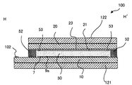
先ず、本実施形態に係る液晶装置を構成する液晶パネルの構成について、図1及び図2を参照して説明する。ここに図1は、本実施形態に係る液晶パネルの全体構成を示す平面図であり、図2は、図1のH−H'線での断面図である。尚、以降の図では、各層・各部材を図面上で認識可能な程度の大きさとするため、図ごとに各層・各部材の縮尺を異ならしめて図示することがある。 First, the configuration of the liquid crystal panel constituting the liquid crystal device according to the present embodiment will be described with reference to FIGS. FIG. 1 is a plan view showing the overall configuration of the liquid crystal panel according to this embodiment, and FIG. 2 is a cross-sectional view taken along the line HH ′ of FIG. In the following drawings, each layer and each member may be illustrated with different scales in order to make each layer and each member recognizable on the drawing.
図1及び図2において、本実施形態に係る液晶パネル100では、TFTアレイ基板10と対向基板20とが対向配置されている。TFTアレイ基板10は、例えば石英基板、ガラス基板等の透明基板や、シリコン基板等である。対向基板20は、例えば石英基板、ガラス基板等の透明基板である。TFTアレイ基板10と対向基板20との間には、液晶層50が封入されている。
1 and 2, in the
TFTアレイ基板10と対向基板20とは、本発明に係る「表示部」の一例としての画像表示領域10aの周囲に位置するシール領域に設けられたシール材52により相互に接着されている。シール材52は、例えば紫外線硬化樹脂からなり、製造プロセスにおいてTFTアレイ基板10上に塗布された後、紫外線照射により硬化させられたものである。また、シール材52中には、TFTアレイ基板10と対向基板20との間隔(基板間ギャップ)を所定値とするためのグラスファイバ或いはガラスビーズ等のギャップ材(図示せず)が散布されている。
The
図1において、シール材52が配置されたシール領域の内側に並行して、画像表示領域10aの額縁領域を規定する遮光性の額縁遮光膜53が、対向基板20側に設けられている。周辺領域のうち、シール材52が配置されたシール領域の外側に位置する領域には、画像信号が供給される画像信号端子を含む外部回路接続端子102がTFTアレイ基板10の一辺に沿って設けられている。
In FIG. 1, a light-shielding frame light-shielding
外部回路接続端子102が設けられた一辺に沿ったシール領域よりも内側には、サンプリング回路7が額縁遮光膜53に覆われるようにして設けられている。走査線駆動回路104は、この一辺に隣接する2辺に沿ったシール領域の内側に、額縁遮光膜53に覆われるようにして設けられている。また、TFTアレイ基板10上には、対向基板20の4つのコーナー部に対向する領域に、両基板間を上下導通材107で接続するための上下導通端子106が配置されている。これらにより、TFTアレイ基板10と対向基板20との間で電気的な導通をとることができる。
The
TFTアレイ基板10上には、外部回路接続端子102と、サンプリング回路7、走査線駆動回路104、上下導通端子106等とを電気的に接続するための引回配線90が形成されている。
On the
図2において、TFTアレイ基板10上には、駆動素子である画素スイッチング用TFTや走査線、データ線等の配線が作り込まれた積層構造が形成される。この積層構造の詳細な説明については図示を省略してあるが、画像表示領域10aには、画素スイッチング用TFTや走査線、データ線等の配線の上層に画素電極9aが設けられている。画素電極9aは典型的にはITO(Indium Tin Oxide)等の透明材料により、画素毎に所定のパターンで島状に形成される。なお、反射型の液晶パネルとする場合は、画素電極9aは、アルミニウム又は銀等の反射性を有する金属材料から形成される。
In FIG. 2, on the
画素電極9a上には、配向膜(図示せず)が形成されている。他方、対向基板20におけるTFTアレイ基板10との対向面上に、遮光膜23が形成されている。そして、遮光膜23上に、ITO等の透明材料からなる対向電極21が複数の画素電極9aと対向して形成されている。対向電極21上には配向膜(図示せず)が形成されている。液晶層50は、例えば一種又は数種類のネマティック液晶を混合した液晶からなり、これら一対の配向膜間で、所定の配向状態をとる。
An alignment film (not shown) is formed on the
液晶パネル100の駆動時において、画素電極9aには画素毎に画像信号が供給され、対向電極21との間で一定期間保持される。このようにして印加される電圧レベルにより、液晶層50を構成する液晶は、分子集合の配向や秩序が変化することにより、光を変調し、階調表示を可能とする。例えば、ノーマリーホワイトモードであれば、各画素の単位で印加された電圧に応じて入射光に対する透過率が減少し、ノーマリーブラックモードであれば、各画素の単位で印加された電圧に応じて入射光に対する透過率が増加され、全体として画像表示領域10aにおいて画像信号に応じたコントラストをもつ光が出射する。尚、詳細な説明は省略するが、各画素はデータ線や走査線に画像信号等の各種信号が供給されることにより駆動され、画素電極9aは画素スイッチング用TFTによりスイッチング制御される。
When the
図2において、TFTアレイ基板10及び対向基板20の各々の液晶層50に対向しない側には、例えばガラス等の透明基板を用いて構成される防塵用基板121及び122が設けられている。この防塵用基板121及び122のデフォーカス作用により、TFTアレイ基板10及び対向基板20の各々の外側表面、即ち、防塵用基板121及び122と貼り合わせられる接着面に付着した埃や塵は、表示画面にピンボケの状態で表示されることとなる。よって、表示画面に、前述したような埃や塵が明確に映りこむのを防止することができる。尚、液晶パネル100は防塵用基板121及び122のほか、反射防止板等の光学要素が設けられるようにしてもよい。
In FIG. 2, dust-
また、ここでは図示しないが、TFTアレイ基板10上には、サンプリング回路7、走査線駆動回路104の他に、製造途中や出荷時の当該液晶装置の品質、欠陥等を検査するための検査回路、検査用パターン等が形成されていてもよい。
Although not shown here, on the
本実施形態に係る液晶装置は、以上に説明したような液晶パネル100が実装ケース内に収容されてなる。以下では、液晶装置の構成について、図3から図15を参照して説明する。
The liquid crystal device according to the present embodiment includes the
<第1実施形態>
先ず、第1実施形態に係る液晶装置の全体構成について、図3から図7を参照して説明する。ここに図3は、第1実施形態に係る液晶装置を光入射側から見た平面図であり、図4は、第1実施形態に係る液晶装置を光出射側から見た平面図である。また図5は、第1実施形態に係る液晶装置を実装ケースの側面側から見た側面図であり、図6は、図5に示す液晶装置を、実装ケースの主要な構成要素ごとに分解した分解側面図である。図7は、図3に示すA0−A0'線における液晶装置の断面部分の構成を示す断面図である。
<First Embodiment>
First, the overall configuration of the liquid crystal device according to the first embodiment will be described with reference to FIGS. FIG. 3 is a plan view of the liquid crystal device according to the first embodiment as viewed from the light incident side, and FIG. 4 is a plan view of the liquid crystal device according to the first embodiment as viewed from the light emission side. FIG. 5 is a side view of the liquid crystal device according to the first embodiment as viewed from the side of the mounting case. FIG. 6 is an exploded view of the liquid crystal device shown in FIG. 5 for each main component of the mounting case. It is an exploded side view. FIG. 7 is a cross-sectional view showing a configuration of a cross-sectional portion of the liquid crystal device taken along line A0-A0 ′ shown in FIG.
図3から図6において、液晶パネル100を収容する実装ケース600は、フレーム610、第1のフック620及び第2のフック630を備えて構成される。尚、第1のフック620は、本発明に係る「第1部材」の一例であり、第2のフック630は、本発明に係る「第2部材」の一例である。
3 to 6, the mounting
フレーム610は、例えば、ダイキャスティング(金型鋳造)により、アルミニウム等の金属から形成されている。またフレーム610には、四隅に取り付け穴616が設けられている。取り付け穴616は、例えばプロジェクター等の機器内に、液晶装置を取り付ける際に利用される。
The
第1のフック620及び第2のフック630は夫々、例えば、プレス加工により、アルミニウム、ステンレス等の金属から形成されている。第1のフック620及び第2のフック630は夫々異なる側からフレーム610に取り付けられる。
The
液晶パネル100への画像信号供給に係る回路部分(即ち、サンプリング回路7を介して各画素に画像信号を供給するためのデータ線駆動回路や画像信号供給回路等を含む回路部分)は、好ましくは駆動用IC(Integrated Circuit)チップ300内に内蔵される。或いは、画像信号供給に係る回路部分の一部が駆動用ICチップ300内に、それ以外の他部がTFTアレイ基板10上に内蔵されるようにしてもよい。
A circuit portion related to image signal supply to the liquid crystal panel 100 (that is, a circuit portion including a data line driving circuit and an image signal supply circuit for supplying an image signal to each pixel via the sampling circuit 7) is preferably It is built in a driving IC (Integrated Circuit)
図7において、液晶パネル100は、外部回路接続端子102において配線基板200を介して駆動用ICチップ300に電気的に接続される。駆動用ICチップ300は例えばTAB(Tape Automated Bonding)技術により配線基板200に固着される。駆動用ICチップ300は、液晶パネル100に画像信号等を含む各種信号を供給するための各種回路が作り込まれている。即ち、図1及び図2を参照して説明した表示動作は、TFTアレイ基板10上の走査線駆動回路104やサンプリング回路7に加えて駆動用ICチップ300により液晶パネル100が駆動されることによりなされる。
In FIG. 7, the
続いて、実装ケース600におけるフレーム610、第1のフック620及び第2のフック630の各々の構成について、既出の図3から図7に加え、図8を参照してより詳細に説明する。ここに図8は、図3に示すB0−B0'線における液晶装置の断面部分の構成を示す断面図である。尚、本実施形態では、第1のフック620側から投射光が入射し、液晶パネル100の画像表示領域10aを透過した後、第2のフック630側から出射されるということを前提とする。
Next, the configuration of each of the
図7及び図8に示すように、フレーム610を構成する部材は、液晶パネル100を収容するためくり抜かれたような状態となっており、これによる開口を開口部615が規定している。フレーム610内の液晶パネル100はその周縁部側から開口部615に包囲され、その開口内に収容される。
As shown in FIGS. 7 and 8, the members constituting the
第1のフック620は板状の部材であって、実装ケース600内において図3、図5及び図6に示すように液晶パネル100の一面に対向して、開口部615を覆うようにフレーム610に対して装着される。第1のフック620は、第1の窓625hを規定する窓部625を有する。窓部625は、第1のフック620を構成する部材が開口形状に形成された一部であり、本発明の「開口部」の一例である。
The
第2のフック630は、第1のフックと同様の板状の部材であって、実装ケース600内において図4、図5及び図6に示すように、第1のフック620とは反対側から、液晶パネル100の他の面に対向して、開口部615を覆うようにフレーム610に対して装着される。第2のフック630は、第2の窓635hを規定する窓部635を有する。窓部635は、第2のフック630を構成する部材が開口形状に形成された一部であり、本発明の「開口部」の一例である。
The
ここで特に、本実施形態に係る液晶装置の窓部625及び635は、夫々台形とされている。即ち、第1の窓625h及び第2の窓635hは台形として規定されている。窓部625及び635を図に示すような台形にすることによる効果は、後に詳述する。なお、反射型の液晶装置とする場合は、窓部625及び635は、入射及び反射側の一方にのみ設けられる。
Here, in particular, the
図5、図6及び図8において、第1のフック620は、それを構成する部材の一部をフレーム610の側面側に折り曲げてなる装着部628を有する。また、フレーム610は爪部619を有する。第1のフック620は、装着部628を爪部619に掛けることによりフレーム610に対して装着される。ここで、装着部628がフレーム610の側面においてその壁部分に接触することにより、第1のフック620からフレーム610への熱伝導が可能となっている。尚、第2のフック630も好ましくは、第1のフック620と同様に爪部619においてフレーム610に対して装着される。
5, 6, and 8, the
第1のフック620は、フレームに610装着された状態では爪部619に掛けられた装着部628により引っ張られるような力が生じ、歪みが生じるおそれがある。このため、装着部628は引っ掛け部626を有し、フレーム610の爪部619が設けられた壁部分には、引っ掛け部626に対応する止め部617が形成されている。引っ掛け部626は、装着部628が爪部619に装着された状態で、装着部628が爪部619により引っ張られる力により止め部617に引っ掛かって止められる。これにより、引っ掛け部626により装着部628が引っ張られる力を緩和することが可能となる。従って、装着部628が爪部619に装着されることで第1のフック620に歪みが生じるのを防止することができる。
When the
次に、本実施形態に係る液晶装置の窓部625及び635がもたらす効果について、既出の図3及び図4に加え、図9から図11を参照して説明する。ここに、図9は、図7に示す断面部分において、例えばプロジェクター等の機器内で供給される冷却風の流れについて説明するための説明図である。また図10及び図11は夫々、第1実施形態に係る液晶装置の変形例を示す平面図である。尚、図9から図11において、冷却風の液晶装置に対する流れの一例は、点線矢印により概略的に示されている。従って、実際の冷却風の流れは図に示す点線矢印とは詳細には異なる場合もある。
Next, effects brought about by the
図9において、本実施形態に係る液晶装置に対しては、冷却風が図の上方向から下方向へと流れるように供給される。冷却風は、例えば冷却ファン等から供給され、液晶パネル100における画像表示領域10a(図1参照)の面に沿う方向に流れる。
In FIG. 9, the cooling air is supplied to the liquid crystal device according to the present embodiment so as to flow from the upper side to the lower side of the figure. The cooling air is supplied from, for example, a cooling fan or the like and flows in a direction along the surface of the
ここで、本願発明者の研究によれば、冷却風の冷却効果は、冷却風の当たりがよい風上側が高く、冷却風の当たりが悪い風下側が低い。このため、液晶パネル100における冷却風の上流側(即ち、図の上方側)の部分は冷却されやすく、下流側(即ち、図の下方側)の部分は冷却され難い状態となってしまう。よって、仮に液晶パネル100が均一に発熱すると考えると、冷却後の液晶パネル100には、冷却風の上流側と下流側とで温度ムラが生じてしまうおそれがある。
Here, according to the study of the present inventor, the cooling effect of the cooling air is high on the windward side where the cooling air hits well and low on the leeward side where the cooling air hits badly. For this reason, the upstream side (that is, the upper side in the figure) of the cooling air in the
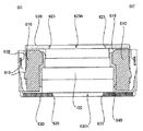
図3及び図4において、本実施形態に係る第1のフック620における窓部625、及び第2のフック630における窓部635は、冷却風の上流側に位置する比較的長い第1辺と、冷却風の下流側に位置する比較的長い第2辺とを有するように構成される。このように構成された窓部625及び635では、図に示すように、冷却風の上流側の方が下流側より大きく開口されることとなる。即ち、窓部625及び635の面積は、冷却風の上流側の方が下流側より大きくされる。よって、液晶パネル100に光が入射可能な面積は、冷却風の上流側の方が下流側より大きくなる。
3 and 4, the
このように構成すれば、冷却風の上流側には、下流側より多くの光が入射することになるため、装置の動作時の発熱量は、冷却風の上流側の方が下流側より大きくなる。即ち、冷却風による冷却効果の高い上流側においては発熱量が大きくなり、冷却効果の低い下流側においては発熱量が小さくなる。よって、冷却後の液晶パネル100における温度ムラを低減することができる。
With this configuration, more light is incident on the upstream side of the cooling air than on the downstream side. Therefore, the amount of heat generated during operation of the apparatus is larger on the upstream side of the cooling air than on the downstream side. Become. In other words, the amount of heat generation increases on the upstream side where the cooling effect by the cooling air is high, and the amount of heat generation decreases on the downstream side where the cooling effect is low. Therefore, temperature unevenness in the
図10及び図11において、冷却風の向きが変化する場合は、第1のフック620における窓部625、及び第2のフック630における窓部635の形状を変化させることによって対応することができる。具体的には、図10に示すように、冷却風が図の下方向から上方向に供給される場合には、冷却風の上流側となる図の下側が大きく開口された窓部625とすればよい。また、図11に示すように、冷却風が図の左方向から右方向に供給される場合には、冷却風の上流側となる図の左側が大きく開口された窓部625とすればよい。
10 and 11, the direction of the cooling air can be changed by changing the shapes of the
尚、実際の冷却効率に基づいて、窓部625及び635の開口面積の大きさを調整するようにすれば、より好適に液晶パネル100における温度ムラを低減することができる。
Note that if the sizes of the opening areas of the
以上説明したように、第1実施形態に係る液晶装置によれば、冷却風の上流側及び下流側の発熱量を調節することで、装置における温度ムラを好適に防止することが可能である。 As described above, according to the liquid crystal device according to the first embodiment, it is possible to suitably prevent temperature unevenness in the device by adjusting the heat generation amount on the upstream side and the downstream side of the cooling air.
<第2実施形態>
次に、第2実施形態に係る液晶装置について、図12から図14を参照して説明する。ここに図12は、第2実施形態に係る液晶装置を実装ケースの側面側から見た側面図である。また図13及び図14は夫々、第2実施形態に係る液晶装置の変形例を示す側面図である。尚、図12以降の図では、説明の便宜上、図11までに図示した詳細な部材を適宜省略して簡略的に図示している。第2実施形態は、上述の第1実施形態と比べて、実装ケース600の一部の構成が異なり、その他の構成については概ね同様である。このため第2実施形態では、第1実施形態と異なる部分について詳細に説明し、その他の重複する部分については適宜説明を省略する。
Second Embodiment
Next, a liquid crystal device according to a second embodiment will be described with reference to FIGS. FIG. 12 is a side view of the liquid crystal device according to the second embodiment as viewed from the side of the mounting case. 13 and 14 are side views showing modifications of the liquid crystal device according to the second embodiment. In FIG. 12 and subsequent figures, for convenience of explanation, detailed members illustrated up to FIG. The second embodiment differs from the first embodiment described above in a part of the configuration of the mounting
図12において、第2実施形態に係る液晶装置は、実装ケース600における冷却風の上流側より下流側の方が盛り上がるように構成されている。具体的には、図を見ても分かるように、実装ケース600における窓部625及び635から見て冷却風の下流側の幅W2は、上流側の幅W1よりも大きい。尚、ここでの実装ケース600における冷却風の下流側部分は、本発明の「凸部」を有する保持部材の一例である。なお、上述の第1実施形態と同様に反射型の液晶装置とする場合は、窓部625及び635は、入射及び反射側の一方にのみ設けられる。
In FIG. 12, the liquid crystal device according to the second embodiment is configured such that the downstream side of the mounting
上述したように構成すれば、冷却風は、液晶パネル100の表面を通過した後、実装ケース600における盛り上がるように形成された部分に当たることになる。従って、冷却風の下流側における放熱効果は、上流側より高いものとなる。具体的には、下流側の部分を盛り上げるように形成することによる表面積の増加や、冷却風の流れる方向の変化により、放熱効果が高められる。
If configured as described above, the cooling air hits a portion formed so as to rise in the mounting
図13に示すように、実装ケース600が盛り上がるように形成されるのは、窓部625及び635のうち一方だけであっても構わない。即ち、図のように、窓部625における冷却風の下流側が盛り上がるように形成される一方で、窓部635側は平坦に形成されてもよい。或いは逆に、窓部635における冷却風の下流側が盛り上がるように形成され、窓部625側は平坦に形成されてもよい。
As shown in FIG. 13, only one of the
このように構成すれば、例えば装置の一方側に他の光学部材を設ける場合等において、好適に装置を配置することが可能となる。即ち、実装ケース600の表面に凹凸を設けることによって、装置が配置し難いような形状となってしまうことを防止することができる。
If comprised in this way, when providing another optical member in the one side of an apparatus, for example, it becomes possible to arrange | position a apparatus suitably. That is, by providing irregularities on the surface of the mounting
図14に示すように、実装ケース600において盛り上がるように形成される部分は、窓部625及び635の境界部分でなくとも構わない。また盛り上がる形状も、図13に示したような垂直に切り立つような形状でなくてよい。
As shown in FIG. 14, the portion formed so as to rise in the mounting
図14に示す形状では、実装ケース600における窓部625及び635から見て冷却風の上流側の幅W1と下流側の幅W2とはほぼ同じ大きさとなる。しかしながらより冷却風の下流側の幅W3は、幅W1や幅W2より大きくなる。従って、冷却風の下流側における放熱効果は、上流側より高いものとなる。
In the shape shown in FIG. 14, the width W1 on the upstream side of the cooling air and the width W2 on the downstream side of the cooling air are almost the same as viewed from the
尚、図13及び図14を用いて説明した変形例は、あくまで一例であり、実装ケース600がここで挙げない形状であったとしても、冷却風の上流側より下流側の方の幅が大きくなるように構成されている限り、上述した本実施形態に係る効果は相応に得られる。
The modification described with reference to FIGS. 13 and 14 is merely an example, and even if the mounting
以上説明したように、第2実施形態に係る液晶装置によれば、第1実施形態に係る液晶装置における台形の窓部による効果と同様の効果を、盛り上がるように形成された実装ケース600においても発揮させることができる。従って、装置における温度ムラをより好適に防止することが可能である。
As described above, according to the liquid crystal device according to the second embodiment, the mounting
<第3実施形態>
次に、第3実施形態に係る液晶装置について、図15を参照して説明する。ここに図15は、第3実施形態に係る液晶装置を実装ケースの側面側から見た側面図である。尚、第3実施形態は、上述の第1及び第2実施形態と比べて、実装ケース600の一部の構成が異なり、その他の構成については概ね同様である。このため第3実施形態では、第1及び第2実施形態と異なる部分について詳細に説明し、その他の重複する部分については適宜説明を省略する。
<Third Embodiment>
Next, a liquid crystal device according to a third embodiment will be described with reference to FIG. FIG. 15 is a side view of the liquid crystal device according to the third embodiment as viewed from the side of the mounting case. Note that the third embodiment differs from the first and second embodiments described above in a part of the configuration of the mounting
図15において、第3実施形態に係る液晶装置は、実装ケース600における窓部625及び635から見て冷却風の上流側の厚みが、液晶パネル100の厚みより小さくなるように構成されている。また、実装ケース600における窓部625及び635から見て冷却風の下流側の厚みが、液晶パネル100の厚みより大きくなるように構成されている。具体的には、液晶パネル100の厚みをW4、実装ケース600における窓部625及び635から見て冷却風の上流側の部分の厚みをW5、実装ケース600における窓部625及び635から見て冷却風の下流側の部分の厚みをW6とすると、W4<W3<W5となるように構成されている。なお、上述の第1実施形態と同様に反射型の液晶装置とする場合は、窓部625及び635は、入射及び反射側の一方にのみ設けられる。
In FIG. 15, the liquid crystal device according to the third embodiment is configured such that the upstream thickness of the cooling air when viewed from the
上述したように構成すれば、第2実施形態に係る液晶装置と同様に、冷却風は、上流側の比較的厚みの小さい実装ケース600部分を通過して、更に液晶パネル100の表面を通過した後、下流側の比較的厚みの大きい実装ケース600部分に当たることになる。従って、冷却風の下流側における放熱効果は、上流側より高いものとなる。具体的には、下流側の部分を盛り上げるように形成することによる表面積の増加や、冷却風の流れる方向の変化により、放熱効果が高められる。
If comprised as mentioned above, like the liquid crystal device according to the second embodiment, the cooling air passed through the mounting
以上説明したように、第3実施形態に係る液晶装置によれば、第2実施形態と同様に、第1実施形態に係る液晶装置における台形の窓部による効果と同様の効果を、厚みを異ならしめて構成された実装ケース600においても発揮させることができる。従って、装置における温度ムラをより好適に防止することが可能である。
As described above, according to the liquid crystal device according to the third embodiment, similar to the second embodiment, the same effect as that of the trapezoidal window in the liquid crystal device according to the first embodiment is obtained with different thicknesses. The present invention can also be exhibited in the mounting
<電子機器>
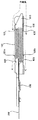
次に、上述した電気光学装置の一例である液晶装置を各種の電子機器に適用する場合について説明する。以下では、この液晶装置をライトバルブとして用いたプロジェクターについて説明する。ここに図16は、プロジェクターの構成例を示す平面図である。また図17及び図18は夫々、図16に示すプロジェクターにおける液晶装置の配置構成を概略的に示す平面図である。
<Electronic equipment>
Next, a case where the liquid crystal device which is an example of the above-described electro-optical device is applied to various electronic devices will be described. Hereinafter, a projector using the liquid crystal device as a light valve will be described. FIG. 16 is a plan view showing a configuration example of the projector. 17 and 18 are plan views schematically showing the arrangement configuration of the liquid crystal device in the projector shown in FIG.
図16に示されるように、プロジェクター1100内部には、ハロゲンランプ等の白色光源からなるランプユニット1102が設けられている。このランプユニット1102から射出された投射光は、ライトガイド1104内に配置された4枚のミラー1106及び2枚のダイクロイックミラー1108によってRGBの3原色に分離され、各原色に対応するライトバルブとしての液晶パネル1110R、1110B及び1110Gに入射される。
As shown in FIG. 16, a
液晶パネル1110R、1110B及び1110Gの構成は、上述した液晶装置と同等であり、画像信号処理回路から供給されるR、G、Bの原色信号でそれぞれ駆動されるものである。そして、これらの液晶パネルによって変調された光は、ダイクロイックプリズム1112に3方向から入射される。このダイクロイックプリズム1112においては、R及びBの光が90度に屈折する一方、Gの光が直進する。従って、各色の画像が合成される結果、投射レンズ1114を介して、スクリーン等にカラー画像が投写されることとなる。
The configurations of the
ここで、各液晶パネル1110R、1110B及び1110Gによる表示像について着目すると、液晶パネル1110Gによる表示像は、液晶パネル1110R、1110Bによる表示像に対して左右反転することが必要となる。
Here, paying attention to the display images by the
尚、液晶パネル1110R、1110B及び1110Gには、ダイクロイックミラー1108によって、R、G、Bの各原色に対応する光が入射するので、カラーフィルターを設ける必要はない。
Since light corresponding to the primary colors R, G, and B is incident on the
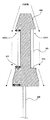
図17及び図18において、第2及び第3実施形態のように実装ケースの厚みを変化させているような場合(図12から図15参照)には、図に示すような向きで液晶パネル1110R、1110B及び1110Gを配置すればよい。
17 and 18, when the thickness of the mounting case is changed as in the second and third embodiments (see FIGS. 12 to 15), the
尚、図16を参照して説明した電子機器の他にも、モバイル型のパーソナルコンピュータや、携帯電話、液晶テレビや、ビューファインダー型、モニタ直視型のビデオテープレコーダー、カーナビゲーション装置、ページャー、電子手帳、電卓、ワードプロセッサー、ワークステーション、テレビ電話、POS端末、タッチパネルを備えた装置等が挙げられる。そして、これらの各種電子機器に適用可能なのは言うまでもない。 In addition to the electronic device described with reference to FIG. 16, a mobile personal computer, a mobile phone, an LCD TV, a viewfinder type, a monitor direct view type video tape recorder, a car navigation device, a pager, an electronic device Examples include notebooks, calculators, word processors, workstations, videophones, POS terminals, and devices with touch panels. Needless to say, the present invention can be applied to these various electronic devices.
また、本発明は上述の各実施形態で説明した液晶装置以外にも反射型液晶装置(LCOS)、プラズマディスプレイ(PDP)、電界放出型ディスプレイ(FED、SED)、有機ELディスプレイ、デジタルマイクロミラーデバイス(DMD)、電気泳動装置等にも適用可能である。 In addition to the liquid crystal devices described in the above embodiments, the present invention includes a reflective liquid crystal device (LCOS), a plasma display (PDP), a field emission display (FED, SED), an organic EL display, and a digital micromirror device. (DMD), electrophoresis apparatus and the like are also applicable.
本発明は、上述した実施形態に限られるものではなく、特許請求の範囲及び明細書全体から読み取れる発明の要旨或いは思想に反しない範囲で適宜変更可能であり、そのような変更を伴う電気光学装置、及び該電気光学装置を備えた電子機器もまた本発明の技術的範囲に含まれるものである。 The present invention is not limited to the above-described embodiments, and can be appropriately changed without departing from the spirit or idea of the invention that can be read from the claims and the entire specification, and an electro-optical device with such a change. In addition, an electronic apparatus including the electro-optical device is also included in the technical scope of the present invention.
10…TFTアレイ基板、20…対向基板、50…液晶層、100…液晶パネル、200…配線基板、300…駆動用ICチップ、600…実装ケース、610…フレーム、620…第1のフック、630…第2のフック、625,635…窓部
DESCRIPTION OF
Claims (6)
前記電気光学パネルを少なくとも部分的に覆うと共に、前記表示部を開口部から露出させるように保持する保持部材と
を備え、
前記開口部は、冷却風の上流側に位置する第1辺及び前記第1辺と対向しており前記第1辺より前記冷却風の下流側に位置する第2辺を有し、
前記第1辺の長さは、前記第2辺の長さよりも長い
ことを特徴とする電気光学装置。 An electro-optical panel having a display for displaying an image;
A holding member that at least partially covers the electro-optical panel and holds the display unit so as to be exposed from the opening,
The opening has a first side located on the upstream side of the cooling air and a second side facing the first side and located on the downstream side of the cooling air from the first side,
The electro-optical device, wherein the length of the first side is longer than the length of the second side.
Priority Applications (1)
| Application Number | Priority Date | Filing Date | Title |
|---|---|---|---|
| JP2010005657A JP5370168B2 (en) | 2010-01-14 | 2010-01-14 | Electro-optical device and electronic apparatus |
Applications Claiming Priority (1)
| Application Number | Priority Date | Filing Date | Title |
|---|---|---|---|
| JP2010005657A JP5370168B2 (en) | 2010-01-14 | 2010-01-14 | Electro-optical device and electronic apparatus |
Publications (2)
| Publication Number | Publication Date |
|---|---|
| JP2011145444A JP2011145444A (en) | 2011-07-28 |
| JP5370168B2 true JP5370168B2 (en) | 2013-12-18 |
Family
ID=44460358
Family Applications (1)
| Application Number | Title | Priority Date | Filing Date |
|---|---|---|---|
| JP2010005657A Expired - Fee Related JP5370168B2 (en) | 2010-01-14 | 2010-01-14 | Electro-optical device and electronic apparatus |
Country Status (1)
| Country | Link |
|---|---|
| JP (1) | JP5370168B2 (en) |
Family Cites Families (4)
| Publication number | Priority date | Publication date | Assignee | Title |
|---|---|---|---|---|
| JP3577698B2 (en) * | 2001-08-03 | 2004-10-13 | 日本航空電子工業株式会社 | Liquid crystal display |
| JP4145595B2 (en) * | 2002-07-30 | 2008-09-03 | 株式会社東芝 | LCD projector |
| JP3092509U (en) * | 2002-09-02 | 2003-03-20 | 船井電機株式会社 | Image display projector using DMD |
| JP2006301256A (en) * | 2005-04-20 | 2006-11-02 | Sony Corp | Apparatus using circuit board and electronic apparatus |
-
2010
- 2010-01-14 JP JP2010005657A patent/JP5370168B2/en not_active Expired - Fee Related
Also Published As
| Publication number | Publication date |
|---|---|
| JP2011145444A (en) | 2011-07-28 |
Similar Documents
| Publication | Publication Date | Title |
|---|---|---|
| JP5504557B2 (en) | Electro-optical device, mounting case for electro-optical device, and electronic apparatus | |
| JP5533001B2 (en) | Electro-optical device and electronic apparatus | |
| US8373806B2 (en) | Electro-optical device and electronic apparatus | |
| CN102193220B (en) | Electro-optic device and electronic apparatus | |
| JP2010102219A (en) | Electrooptical device and electronic apparatus | |
| JP5109713B2 (en) | Electro-optical device and electronic apparatus | |
| JP5544749B2 (en) | Electro-optical device and electronic apparatus | |
| JP5287119B2 (en) | Electro-optical device and electronic apparatus | |
| JP2010256666A (en) | Electro-optical device and electronic apparatus | |
| JP2007279626A (en) | Electro-optical device and electronic apparatus including the same | |
| JP5370168B2 (en) | Electro-optical device and electronic apparatus | |
| JP2010256662A (en) | Electro-optical device and electronic apparatus | |
| JP2010256667A (en) | Electro-optical device and electronic apparatus | |
| JP2011145445A (en) | Electro-optical device and electronic apparatus | |
| JP2011145446A (en) | Electro-optical device and electronic apparatus | |
| JP6269749B2 (en) | Electro-optical device and electronic apparatus | |
| JP5834402B2 (en) | Electro-optical device and electronic apparatus | |
| JP5994907B2 (en) | Electro-optical device and electronic apparatus | |
| JP5332482B2 (en) | Electro-optical device and electronic apparatus | |
| JP2010256663A (en) | Electro-optical device and electronic apparatus | |
| JP2009128665A (en) | Electro-optical device and electronic apparatus | |
| JP2010113187A (en) | Electro-optical device and electronic equipment | |
| JP2010060968A (en) | Electro-optical device and electronic apparatus | |
| JP2009075389A (en) | Electro-optical device and electronic apparatus | |
| JP2010175889A (en) | Electro-optical device and electronic apparatus |
Legal Events
| Date | Code | Title | Description |
|---|---|---|---|
| A621 | Written request for application examination |
Free format text: JAPANESE INTERMEDIATE CODE: A621 Effective date: 20121227 |
|
| A977 | Report on retrieval |
Free format text: JAPANESE INTERMEDIATE CODE: A971007 Effective date: 20130809 |
|
| TRDD | Decision of grant or rejection written | ||
| A01 | Written decision to grant a patent or to grant a registration (utility model) |
Free format text: JAPANESE INTERMEDIATE CODE: A01 Effective date: 20130820 |
|
| A61 | First payment of annual fees (during grant procedure) |
Free format text: JAPANESE INTERMEDIATE CODE: A61 Effective date: 20130902 |
|
| R150 | Certificate of patent or registration of utility model |
Ref document number: 5370168 Country of ref document: JP Free format text: JAPANESE INTERMEDIATE CODE: R150 Free format text: JAPANESE INTERMEDIATE CODE: R150 |
|
| S531 | Written request for registration of change of domicile |
Free format text: JAPANESE INTERMEDIATE CODE: R313531 |
|
| R350 | Written notification of registration of transfer |
Free format text: JAPANESE INTERMEDIATE CODE: R350 |
|
| LAPS | Cancellation because of no payment of annual fees |