JP5328276B2 - Method for manufacturing semiconductor device - Google Patents
Method for manufacturing semiconductor device Download PDFInfo
- Publication number
- JP5328276B2 JP5328276B2 JP2008245254A JP2008245254A JP5328276B2 JP 5328276 B2 JP5328276 B2 JP 5328276B2 JP 2008245254 A JP2008245254 A JP 2008245254A JP 2008245254 A JP2008245254 A JP 2008245254A JP 5328276 B2 JP5328276 B2 JP 5328276B2
- Authority
- JP
- Japan
- Prior art keywords
- layer
- insulating layer
- storage capacitor
- single crystal
- crystal silicon
- Prior art date
- Legal status (The legal status is an assumption and is not a legal conclusion. Google has not performed a legal analysis and makes no representation as to the accuracy of the status listed.)
- Expired - Fee Related
Links
- 238000000034 method Methods 0.000 title claims description 33
- 239000004065 semiconductor Substances 0.000 title claims description 29
- 238000004519 manufacturing process Methods 0.000 title claims description 21
- 239000010410 layer Substances 0.000 claims description 217
- 239000000758 substrate Substances 0.000 claims description 134
- 239000003990 capacitor Substances 0.000 claims description 119
- 238000003860 storage Methods 0.000 claims description 102
- 229910021421 monocrystalline silicon Inorganic materials 0.000 claims description 71
- 238000010438 heat treatment Methods 0.000 claims description 48
- 239000012535 impurity Substances 0.000 claims description 40
- 150000002500 ions Chemical class 0.000 claims description 31
- SIWVEOZUMHYXCS-UHFFFAOYSA-N oxo(oxoyttriooxy)yttrium Chemical compound O=[Y]O[Y]=O SIWVEOZUMHYXCS-UHFFFAOYSA-N 0.000 claims description 19
- XUIMIQQOPSSXEZ-UHFFFAOYSA-N Silicon Chemical compound [Si] XUIMIQQOPSSXEZ-UHFFFAOYSA-N 0.000 claims description 13
- 239000013078 crystal Substances 0.000 claims description 13
- 239000011229 interlayer Substances 0.000 claims description 13
- 229910052710 silicon Inorganic materials 0.000 claims description 13
- 239000010703 silicon Substances 0.000 claims description 13
- 239000001257 hydrogen Substances 0.000 claims description 12
- 229910052739 hydrogen Inorganic materials 0.000 claims description 12
- 239000011241 protective layer Substances 0.000 claims description 12
- 229910021419 crystalline silicon Inorganic materials 0.000 claims description 9
- RVTZCBVAJQQJTK-UHFFFAOYSA-N oxygen(2-);zirconium(4+) Chemical compound [O-2].[O-2].[Zr+4] RVTZCBVAJQQJTK-UHFFFAOYSA-N 0.000 claims description 9
- 229910001928 zirconium oxide Inorganic materials 0.000 claims description 9
- 238000005530 etching Methods 0.000 claims description 4
- 125000004435 hydrogen atom Chemical class [H]* 0.000 claims 2
- 238000010030 laminating Methods 0.000 claims 2
- 239000002356 single layer Substances 0.000 claims 1
- 239000010408 film Substances 0.000 description 84
- 239000011521 glass Substances 0.000 description 21
- 239000000463 material Substances 0.000 description 12
- 125000004429 atom Chemical group 0.000 description 8
- VYPSYNLAJGMNEJ-UHFFFAOYSA-N silicon dioxide Inorganic materials O=[Si]=O VYPSYNLAJGMNEJ-UHFFFAOYSA-N 0.000 description 8
- 230000006870 function Effects 0.000 description 7
- 239000007789 gas Substances 0.000 description 7
- 229910052814 silicon oxide Inorganic materials 0.000 description 7
- 239000000126 substance Substances 0.000 description 7
- 230000015572 biosynthetic process Effects 0.000 description 6
- 229910052581 Si3N4 Inorganic materials 0.000 description 5
- QVGXLLKOCUKJST-UHFFFAOYSA-N atomic oxygen Chemical compound [O] QVGXLLKOCUKJST-UHFFFAOYSA-N 0.000 description 5
- 230000014759 maintenance of location Effects 0.000 description 5
- 239000001301 oxygen Substances 0.000 description 5
- 229910052760 oxygen Inorganic materials 0.000 description 5
- 238000000926 separation method Methods 0.000 description 5
- HQVNEWCFYHHQES-UHFFFAOYSA-N silicon nitride Chemical compound N12[Si]34N5[Si]62N3[Si]51N64 HQVNEWCFYHHQES-UHFFFAOYSA-N 0.000 description 5
- XKRFYHLGVUSROY-UHFFFAOYSA-N Argon Chemical compound [Ar] XKRFYHLGVUSROY-UHFFFAOYSA-N 0.000 description 4
- IJGRMHOSHXDMSA-UHFFFAOYSA-N Atomic nitrogen Chemical compound N#N IJGRMHOSHXDMSA-UHFFFAOYSA-N 0.000 description 4
- OAICVXFJPJFONN-UHFFFAOYSA-N Phosphorus Chemical compound [P] OAICVXFJPJFONN-UHFFFAOYSA-N 0.000 description 4
- 238000001312 dry etching Methods 0.000 description 4
- -1 hydrogen ions Chemical class 0.000 description 4
- 229910052698 phosphorus Inorganic materials 0.000 description 4
- 239000011574 phosphorus Substances 0.000 description 4
- 239000010936 titanium Substances 0.000 description 4
- ZOXJGFHDIHLPTG-UHFFFAOYSA-N Boron Chemical compound [B] ZOXJGFHDIHLPTG-UHFFFAOYSA-N 0.000 description 3
- UFHFLCQGNIYNRP-UHFFFAOYSA-N Hydrogen Chemical compound [H][H] UFHFLCQGNIYNRP-UHFFFAOYSA-N 0.000 description 3
- RTAQQCXQSZGOHL-UHFFFAOYSA-N Titanium Chemical compound [Ti] RTAQQCXQSZGOHL-UHFFFAOYSA-N 0.000 description 3
- 230000001133 acceleration Effects 0.000 description 3
- 229910052782 aluminium Inorganic materials 0.000 description 3
- XAGFODPZIPBFFR-UHFFFAOYSA-N aluminium Chemical compound [Al] XAGFODPZIPBFFR-UHFFFAOYSA-N 0.000 description 3
- 238000004458 analytical method Methods 0.000 description 3
- 229910052796 boron Inorganic materials 0.000 description 3
- 238000006243 chemical reaction Methods 0.000 description 3
- 238000005229 chemical vapour deposition Methods 0.000 description 3
- 238000004891 communication Methods 0.000 description 3
- 238000000151 deposition Methods 0.000 description 3
- 230000008021 deposition Effects 0.000 description 3
- 238000010586 diagram Methods 0.000 description 3
- GPRLSGONYQIRFK-UHFFFAOYSA-N hydron Chemical compound [H+] GPRLSGONYQIRFK-UHFFFAOYSA-N 0.000 description 3
- 238000005468 ion implantation Methods 0.000 description 3
- 238000010884 ion-beam technique Methods 0.000 description 3
- 229910052751 metal Inorganic materials 0.000 description 3
- 239000002184 metal Substances 0.000 description 3
- 230000010355 oscillation Effects 0.000 description 3
- 238000005498 polishing Methods 0.000 description 3
- 229910021426 porous silicon Inorganic materials 0.000 description 3
- 230000008569 process Effects 0.000 description 3
- 238000004151 rapid thermal annealing Methods 0.000 description 3
- 238000004544 sputter deposition Methods 0.000 description 3
- 229910052719 titanium Inorganic materials 0.000 description 3
- WZJUBBHODHNQPW-UHFFFAOYSA-N 2,4,6,8-tetramethyl-1,3,5,7,2$l^{3},4$l^{3},6$l^{3},8$l^{3}-tetraoxatetrasilocane Chemical compound C[Si]1O[Si](C)O[Si](C)O[Si](C)O1 WZJUBBHODHNQPW-UHFFFAOYSA-N 0.000 description 2
- 102100040844 Dual specificity protein kinase CLK2 Human genes 0.000 description 2
- 101000749291 Homo sapiens Dual specificity protein kinase CLK2 Proteins 0.000 description 2
- ZOKXTWBITQBERF-UHFFFAOYSA-N Molybdenum Chemical compound [Mo] ZOKXTWBITQBERF-UHFFFAOYSA-N 0.000 description 2
- 239000004642 Polyimide Substances 0.000 description 2
- BOTDANWDWHJENH-UHFFFAOYSA-N Tetraethyl orthosilicate Chemical compound CCO[Si](OCC)(OCC)OCC BOTDANWDWHJENH-UHFFFAOYSA-N 0.000 description 2
- MXSJNBRAMXILSE-UHFFFAOYSA-N [Si].[P].[B] Chemical compound [Si].[P].[B] MXSJNBRAMXILSE-UHFFFAOYSA-N 0.000 description 2
- 239000003513 alkali Substances 0.000 description 2
- 239000005407 aluminoborosilicate glass Substances 0.000 description 2
- 239000005354 aluminosilicate glass Substances 0.000 description 2
- 229910052786 argon Inorganic materials 0.000 description 2
- 229910052788 barium Inorganic materials 0.000 description 2
- DSAJWYNOEDNPEQ-UHFFFAOYSA-N barium atom Chemical compound [Ba] DSAJWYNOEDNPEQ-UHFFFAOYSA-N 0.000 description 2
- 239000002585 base Substances 0.000 description 2
- 230000005540 biological transmission Effects 0.000 description 2
- 239000005388 borosilicate glass Substances 0.000 description 2
- 238000004364 calculation method Methods 0.000 description 2
- 230000008859 change Effects 0.000 description 2
- 238000003776 cleavage reaction Methods 0.000 description 2
- 229910052736 halogen Inorganic materials 0.000 description 2
- 150000002367 halogens Chemical class 0.000 description 2
- 230000005660 hydrophilic surface Effects 0.000 description 2
- 230000001771 impaired effect Effects 0.000 description 2
- 230000006872 improvement Effects 0.000 description 2
- 239000011261 inert gas Substances 0.000 description 2
- 239000012212 insulator Substances 0.000 description 2
- 229910052750 molybdenum Inorganic materials 0.000 description 2
- 239000011733 molybdenum Substances 0.000 description 2
- 229910052757 nitrogen Inorganic materials 0.000 description 2
- HMMGMWAXVFQUOA-UHFFFAOYSA-N octamethylcyclotetrasiloxane Chemical compound C[Si]1(C)O[Si](C)(C)O[Si](C)(C)O[Si](C)(C)O1 HMMGMWAXVFQUOA-UHFFFAOYSA-N 0.000 description 2
- 238000001020 plasma etching Methods 0.000 description 2
- 229920001721 polyimide Polymers 0.000 description 2
- 239000011347 resin Substances 0.000 description 2
- 229920005989 resin Polymers 0.000 description 2
- 230000007017 scission Effects 0.000 description 2
- CZDYPVPMEAXLPK-UHFFFAOYSA-N tetramethylsilane Chemical compound C[Si](C)(C)C CZDYPVPMEAXLPK-UHFFFAOYSA-N 0.000 description 2
- 239000010409 thin film Substances 0.000 description 2
- WFKWXMTUELFFGS-UHFFFAOYSA-N tungsten Chemical compound [W] WFKWXMTUELFFGS-UHFFFAOYSA-N 0.000 description 2
- 229910052721 tungsten Inorganic materials 0.000 description 2
- 239000010937 tungsten Substances 0.000 description 2
- 229910052727 yttrium Inorganic materials 0.000 description 2
- VWQVUPCCIRVNHF-UHFFFAOYSA-N yttrium atom Chemical compound [Y] VWQVUPCCIRVNHF-UHFFFAOYSA-N 0.000 description 2
- 229910000838 Al alloy Inorganic materials 0.000 description 1
- VYZAMTAEIAYCRO-UHFFFAOYSA-N Chromium Chemical compound [Cr] VYZAMTAEIAYCRO-UHFFFAOYSA-N 0.000 description 1
- YZCKVEUIGOORGS-OUBTZVSYSA-N Deuterium Chemical compound [2H] YZCKVEUIGOORGS-OUBTZVSYSA-N 0.000 description 1
- 102100040862 Dual specificity protein kinase CLK1 Human genes 0.000 description 1
- PXGOKWXKJXAPGV-UHFFFAOYSA-N Fluorine Chemical compound FF PXGOKWXKJXAPGV-UHFFFAOYSA-N 0.000 description 1
- GYHNNYVSQQEPJS-UHFFFAOYSA-N Gallium Chemical compound [Ga] GYHNNYVSQQEPJS-UHFFFAOYSA-N 0.000 description 1
- 101000749294 Homo sapiens Dual specificity protein kinase CLK1 Proteins 0.000 description 1
- CBENFWSGALASAD-UHFFFAOYSA-N Ozone Chemical compound [O-][O+]=O CBENFWSGALASAD-UHFFFAOYSA-N 0.000 description 1
- BLRPTPMANUNPDV-UHFFFAOYSA-N Silane Chemical compound [SiH4] BLRPTPMANUNPDV-UHFFFAOYSA-N 0.000 description 1
- QCWXUUIWCKQGHC-UHFFFAOYSA-N Zirconium Chemical compound [Zr] QCWXUUIWCKQGHC-UHFFFAOYSA-N 0.000 description 1
- 230000004913 activation Effects 0.000 description 1
- 239000000654 additive Substances 0.000 description 1
- 238000000137 annealing Methods 0.000 description 1
- 229910052785 arsenic Inorganic materials 0.000 description 1
- RQNWIZPPADIBDY-UHFFFAOYSA-N arsenic atom Chemical compound [As] RQNWIZPPADIBDY-UHFFFAOYSA-N 0.000 description 1
- 230000004888 barrier function Effects 0.000 description 1
- 239000000919 ceramic Substances 0.000 description 1
- 239000003985 ceramic capacitor Substances 0.000 description 1
- 229910052804 chromium Inorganic materials 0.000 description 1
- 239000011651 chromium Substances 0.000 description 1
- 239000011248 coating agent Substances 0.000 description 1
- 238000000576 coating method Methods 0.000 description 1
- 238000005520 cutting process Methods 0.000 description 1
- 229910052805 deuterium Inorganic materials 0.000 description 1
- 230000000694 effects Effects 0.000 description 1
- 230000005684 electric field Effects 0.000 description 1
- 238000005485 electric heating Methods 0.000 description 1
- 238000005516 engineering process Methods 0.000 description 1
- 229910052731 fluorine Inorganic materials 0.000 description 1
- 239000011737 fluorine Substances 0.000 description 1
- 229910052733 gallium Inorganic materials 0.000 description 1
- FFUAGWLWBBFQJT-UHFFFAOYSA-N hexamethyldisilazane Chemical compound C[Si](C)(C)N[Si](C)(C)C FFUAGWLWBBFQJT-UHFFFAOYSA-N 0.000 description 1
- 150000002431 hydrogen Chemical class 0.000 description 1
- 125000002887 hydroxy group Chemical group [H]O* 0.000 description 1
- 230000010354 integration Effects 0.000 description 1
- 230000001678 irradiating effect Effects 0.000 description 1
- 239000004973 liquid crystal related substance Substances 0.000 description 1
- 230000006386 memory function Effects 0.000 description 1
- 238000002156 mixing Methods 0.000 description 1
- 239000000203 mixture Substances 0.000 description 1
- 230000007935 neutral effect Effects 0.000 description 1
- 150000004767 nitrides Chemical class 0.000 description 1
- 150000001282 organosilanes Chemical class 0.000 description 1
- 230000001590 oxidative effect Effects 0.000 description 1
- 230000003071 parasitic effect Effects 0.000 description 1
- 230000035515 penetration Effects 0.000 description 1
- 230000002093 peripheral effect Effects 0.000 description 1
- 238000009832 plasma treatment Methods 0.000 description 1
- 230000001681 protective effect Effects 0.000 description 1
- 239000010453 quartz Substances 0.000 description 1
- 230000005855 radiation Effects 0.000 description 1
- 239000002994 raw material Substances 0.000 description 1
- 239000003870 refractory metal Substances 0.000 description 1
- 230000004044 response Effects 0.000 description 1
- 229910000077 silane Inorganic materials 0.000 description 1
- 239000002210 silicon-based material Substances 0.000 description 1
- 238000004381 surface treatment Methods 0.000 description 1
- 229910052715 tantalum Inorganic materials 0.000 description 1
- GUVRBAGPIYLISA-UHFFFAOYSA-N tantalum atom Chemical compound [Ta] GUVRBAGPIYLISA-UHFFFAOYSA-N 0.000 description 1
- QQQSFSZALRVCSZ-UHFFFAOYSA-N triethoxysilane Chemical compound CCO[SiH](OCC)OCC QQQSFSZALRVCSZ-UHFFFAOYSA-N 0.000 description 1
- XLYOFNOQVPJJNP-UHFFFAOYSA-N water Substances O XLYOFNOQVPJJNP-UHFFFAOYSA-N 0.000 description 1
- 229910052845 zircon Inorganic materials 0.000 description 1
- 229910052726 zirconium Inorganic materials 0.000 description 1
- GFQYVLUOOAAOGM-UHFFFAOYSA-N zirconium(iv) silicate Chemical compound [Zr+4].[O-][Si]([O-])([O-])[O-] GFQYVLUOOAAOGM-UHFFFAOYSA-N 0.000 description 1
Images


Classifications
-
- H—ELECTRICITY
- H01—ELECTRIC ELEMENTS
- H01L—SEMICONDUCTOR DEVICES NOT COVERED BY CLASS H10
- H01L27/00—Devices consisting of a plurality of semiconductor or other solid-state components formed in or on a common substrate
- H01L27/02—Devices consisting of a plurality of semiconductor or other solid-state components formed in or on a common substrate including semiconductor components specially adapted for rectifying, oscillating, amplifying or switching and having at least one potential-jump barrier or surface barrier; including integrated passive circuit elements with at least one potential-jump barrier or surface barrier
- H01L27/12—Devices consisting of a plurality of semiconductor or other solid-state components formed in or on a common substrate including semiconductor components specially adapted for rectifying, oscillating, amplifying or switching and having at least one potential-jump barrier or surface barrier; including integrated passive circuit elements with at least one potential-jump barrier or surface barrier the substrate being other than a semiconductor body, e.g. an insulating body
- H01L27/1214—Devices consisting of a plurality of semiconductor or other solid-state components formed in or on a common substrate including semiconductor components specially adapted for rectifying, oscillating, amplifying or switching and having at least one potential-jump barrier or surface barrier; including integrated passive circuit elements with at least one potential-jump barrier or surface barrier the substrate being other than a semiconductor body, e.g. an insulating body comprising a plurality of TFTs formed on a non-semiconducting substrate, e.g. driving circuits for AMLCDs
- H01L27/1259—Multistep manufacturing methods
- H01L27/1262—Multistep manufacturing methods with a particular formation, treatment or coating of the substrate
- H01L27/1266—Multistep manufacturing methods with a particular formation, treatment or coating of the substrate the substrate on which the devices are formed not being the final device substrate, e.g. using a temporary substrate
-
- H—ELECTRICITY
- H01—ELECTRIC ELEMENTS
- H01L—SEMICONDUCTOR DEVICES NOT COVERED BY CLASS H10
- H01L27/00—Devices consisting of a plurality of semiconductor or other solid-state components formed in or on a common substrate
- H01L27/02—Devices consisting of a plurality of semiconductor or other solid-state components formed in or on a common substrate including semiconductor components specially adapted for rectifying, oscillating, amplifying or switching and having at least one potential-jump barrier or surface barrier; including integrated passive circuit elements with at least one potential-jump barrier or surface barrier
- H01L27/12—Devices consisting of a plurality of semiconductor or other solid-state components formed in or on a common substrate including semiconductor components specially adapted for rectifying, oscillating, amplifying or switching and having at least one potential-jump barrier or surface barrier; including integrated passive circuit elements with at least one potential-jump barrier or surface barrier the substrate being other than a semiconductor body, e.g. an insulating body
- H01L27/1214—Devices consisting of a plurality of semiconductor or other solid-state components formed in or on a common substrate including semiconductor components specially adapted for rectifying, oscillating, amplifying or switching and having at least one potential-jump barrier or surface barrier; including integrated passive circuit elements with at least one potential-jump barrier or surface barrier the substrate being other than a semiconductor body, e.g. an insulating body comprising a plurality of TFTs formed on a non-semiconducting substrate, e.g. driving circuits for AMLCDs
- H01L27/1255—Devices consisting of a plurality of semiconductor or other solid-state components formed in or on a common substrate including semiconductor components specially adapted for rectifying, oscillating, amplifying or switching and having at least one potential-jump barrier or surface barrier; including integrated passive circuit elements with at least one potential-jump barrier or surface barrier the substrate being other than a semiconductor body, e.g. an insulating body comprising a plurality of TFTs formed on a non-semiconducting substrate, e.g. driving circuits for AMLCDs integrated with passive devices, e.g. auxiliary capacitors
-
- H—ELECTRICITY
- H01—ELECTRIC ELEMENTS
- H01L—SEMICONDUCTOR DEVICES NOT COVERED BY CLASS H10
- H01L29/00—Semiconductor devices adapted for rectifying, amplifying, oscillating or switching, or capacitors or resistors with at least one potential-jump barrier or surface barrier, e.g. PN junction depletion layer or carrier concentration layer; Details of semiconductor bodies or of electrodes thereof ; Multistep manufacturing processes therefor
- H01L29/02—Semiconductor bodies ; Multistep manufacturing processes therefor
- H01L29/04—Semiconductor bodies ; Multistep manufacturing processes therefor characterised by their crystalline structure, e.g. polycrystalline, cubic or particular orientation of crystalline planes
-
- H—ELECTRICITY
- H01—ELECTRIC ELEMENTS
- H01L—SEMICONDUCTOR DEVICES NOT COVERED BY CLASS H10
- H01L29/00—Semiconductor devices adapted for rectifying, amplifying, oscillating or switching, or capacitors or resistors with at least one potential-jump barrier or surface barrier, e.g. PN junction depletion layer or carrier concentration layer; Details of semiconductor bodies or of electrodes thereof ; Multistep manufacturing processes therefor
- H01L29/66—Types of semiconductor device ; Multistep manufacturing processes therefor
- H01L29/68—Types of semiconductor device ; Multistep manufacturing processes therefor controllable by only the electric current supplied, or only the electric potential applied, to an electrode which does not carry the current to be rectified, amplified or switched
- H01L29/76—Unipolar devices, e.g. field effect transistors
- H01L29/772—Field effect transistors
- H01L29/78—Field effect transistors with field effect produced by an insulated gate
- H01L29/786—Thin film transistors, i.e. transistors with a channel being at least partly a thin film
- H01L29/78651—Silicon transistors
- H01L29/78654—Monocrystalline silicon transistors
Description
本発明は半導体装置及びその作製方法に関する。特に結晶性半導体基板から半導体層を薄片化して異種基板に接合するSOI(Silicon On Insulator(シリコン・オン・インシュレータ))構造を有する基板に関する。特に貼り合わせSOI技術に関するものであって、ガラス等の絶縁表面を有する基板に単結晶もしくは多結晶の半導体層を接合させたSOI基板の製造方法に関する。また、このようなSOI構造を有する表示装置もしくは半導体装置に関する。 The present invention relates to a semiconductor device and a manufacturing method thereof. In particular, the present invention relates to a substrate having an SOI (Silicon On Insulator) structure in which a semiconductor layer is thinned from a crystalline semiconductor substrate and bonded to a different substrate. In particular, the present invention relates to a bonded SOI technology, and more particularly to a method for manufacturing an SOI substrate in which a single crystal or polycrystalline semiconductor layer is bonded to a substrate having an insulating surface such as glass. Further, the present invention relates to a display device or a semiconductor device having such an SOI structure.
単結晶半導体のインゴットを薄く切断して作製されるシリコンウエハに代わり、絶縁層の上に薄い単結晶半導体層を設けたシリコン・オン・インシュレータ(Silicon On Insulator)と呼ばれる半導体基板(SOI基板)が開発されており、マイクロプロセッサなどを製造する際の基板として普及しつつある。これは、SOI基板を使った集積回路はトランジスタのドレインと基板間における寄生容量を低減し、半導体集積回路の性能を向上させ、低消費電力化を図るものとして注目されているからである。 Instead of a silicon wafer produced by thinly cutting a single crystal semiconductor ingot, a semiconductor substrate (SOI substrate) called a silicon on insulator having a thin single crystal semiconductor layer on an insulating layer is provided. It has been developed and is becoming popular as a substrate for manufacturing microprocessors and the like. This is because integrated circuits using an SOI substrate are attracting attention as reducing parasitic capacitance between the drain of the transistor and the substrate, improving the performance of the semiconductor integrated circuit, and reducing power consumption.
SOI基板を製造する方法としては、水素イオン注入剥離法が知られている(例えば、特許文献1参照)。水素イオン注入剥離法は、シリコンウエハに水素イオンを注入することによって表面から所定の深さに微小気泡層を形成し、該微小気泡層を劈開面とすることで、別のシリコンウエハに薄いシリコン層(SOI層)を接合する。さらにSOI層を剥離する熱処理を行うことに加え、酸化性雰囲気下での熱処理によりSOI層に酸化膜を形成した後に該酸化膜を除去し、次に1000℃以上1300℃以下の還元性雰囲気下で熱処理を行って接合強度を高める必要があるとされている。 As a method for manufacturing an SOI substrate, a hydrogen ion implantation separation method is known (for example, see Patent Document 1). In the hydrogen ion implantation separation method, a microbubble layer is formed at a predetermined depth from the surface by injecting hydrogen ions into a silicon wafer, and the microbubble layer is used as a cleavage plane, so that a thin silicon film is formed on another silicon wafer. Bond layers (SOI layers). Further, in addition to performing heat treatment for peeling off the SOI layer, after forming an oxide film on the SOI layer by heat treatment in an oxidizing atmosphere, the oxide film is removed, and then in a reducing atmosphere at 1000 ° C. to 1300 ° C. It is said that it is necessary to increase the bonding strength by performing a heat treatment.
一方、ガラスなどの絶縁基板にSOI層を形成しようとする試みもなされている。ガラス基板上にSOI層を形成したSOI基板の一例として、水素イオン注入剥離法を用いて、コーティング膜を有するガラス基板上に薄い単結晶シリコン層を形成したものが知られている(特許文献2及び特許文献3参照)。この場合にも、単結晶シリコン片に水素イオンを注入することによって表面から所定の深さに微小気泡層を形成し、ガラス基板と単結晶シリコン片を張り合わせ後に、微小気泡層を劈開面としてシリコン片を剥離することで、ガラス基板上に薄いシリコン層(SOI層)を形成している。 On the other hand, attempts have been made to form an SOI layer on an insulating substrate such as glass. As an example of an SOI substrate in which an SOI layer is formed on a glass substrate, a thin single crystal silicon layer formed on a glass substrate having a coating film by using a hydrogen ion implantation separation method is known (Patent Document 2). And Patent Document 3). Also in this case, a microbubble layer is formed at a predetermined depth from the surface by implanting hydrogen ions into the single crystal silicon piece, and after bonding the glass substrate and the single crystal silicon piece, the microbubble layer is used as a cleavage plane to form silicon. A thin silicon layer (SOI layer) is formed on the glass substrate by peeling the piece.
ガラス基板などの絶縁基板上に薄膜トランジスタ(Thin Film Transistor(TFT))の構造として、ガラス基板上に、下地絶縁膜、活性層、ゲート絶縁膜、ゲート電極、層間絶縁膜、配線を形成した構造が挙げられる。TFTの応答速度を上げるために、TFT全体のデザインルールを縮小することが行われている。
集積回路のデザインルールを縮小して集積度を高くする場合、容量部の面積を縮小することが有効である。容量部の面積を縮小しつつ必要な容量を確保するためには容量素子の誘電体層を薄くする方法が挙げられる。しかし、誘電体層を薄くするとリーク電流が増えて容量素子の特性が低下してしまう。そこで、誘電体層を薄く形成することなく必要な容量を確保することで、容量部の面積を縮小することを目的の一とする。 In order to increase the degree of integration by reducing the design rule of the integrated circuit, it is effective to reduce the area of the capacitor portion. In order to secure the necessary capacitance while reducing the area of the capacitor portion, a method of thinning the dielectric layer of the capacitor element can be mentioned. However, if the dielectric layer is thinned, the leakage current increases and the characteristics of the capacitive element deteriorate. Thus, an object is to reduce the area of the capacitor portion by securing a necessary capacitance without forming a thin dielectric layer.
また、ガラス基板は、概ね700℃以上の高温熱処理を行うことができない。そのため、ガラス基板上に容量素子の誘電体層を成膜し、高温処理することが困難であった。そこで、本発明は耐熱温度の低い基板上であっても高温処理が必要な誘電体層を形成することを目的の一とする。 Further, the glass substrate cannot be subjected to high temperature heat treatment at about 700 ° C. or higher. For this reason, it is difficult to form a dielectric layer of a capacitive element on a glass substrate and perform high temperature treatment. Therefore, an object of the present invention is to form a dielectric layer that requires high-temperature treatment even on a substrate having a low heat-resistant temperature.
本発明は、容量部に、比誘電率が10以上の材料、例えばイットリウム酸化物、若しくはイットリウム酸化物とジルコニウム酸化物とを含む誘電体層を有する半導体装置である。 The present invention is a semiconductor device having a dielectric layer including a material having a relative dielectric constant of 10 or more, for example, yttrium oxide, or yttrium oxide and zirconium oxide, in a capacitor portion.
本発明の半導体装置は、保持容量部の絶縁膜を単結晶シリコン基板上に成膜し、熱処理して形成する。前記保持容量部の絶縁膜は単結晶シリコン上での特有の結晶成長を得、比誘電率を高めることで、保持容量部の面積を小さくできる。また、保持容量部の絶縁膜の膜厚を小さくせずに設計できるため、電荷保持に優れた保持容量部を形成することができる。また本発明の半導体装置の一は、前記保持容量部の絶縁膜を単結晶シリコン基板から分離し、支持基板上に設けることを特徴とする。また本発明の半導体装置の一は、前記保持容量部の絶縁膜は、支持基板上に設けられた第1の絶縁層上の、第2の絶縁層に埋め込まれていることを特徴とする。 In the semiconductor device of the present invention, the insulating film of the storage capacitor portion is formed over a single crystal silicon substrate and is heat-treated. The insulating film of the storage capacitor portion can obtain a specific crystal growth on single crystal silicon and increase the relative dielectric constant, thereby reducing the area of the storage capacitor portion. In addition, since it is possible to design the storage capacitor portion without reducing the thickness of the insulating film, it is possible to form a storage capacitor portion having excellent charge retention. One feature of the semiconductor device of the present invention is that the insulating film of the storage capacitor portion is separated from the single crystal silicon substrate and provided over a supporting substrate. According to another aspect of the semiconductor device of the present invention, the insulating film of the storage capacitor portion is embedded in a second insulating layer on a first insulating layer provided over a supporting substrate.
前記保持容量部の絶縁膜として、イットリウム酸化物、もしくはイットリウム酸化物に化学的安定のためジルコニウム酸化物を混合した材料を用いる。ここで、本発明の前記保持容量部の絶縁膜は、単結晶シリコン上にスパッタもしくはCVDにて成膜され、750℃以上にて熱処理された後、ガラス基板に張り合わせられる。さらに前記保持容量部の絶縁膜に接する電極と相まって、信頼性の高い保持容量という機能を実現する。 As the insulating film of the storage capacitor portion, yttrium oxide or a material obtained by mixing zirconium oxide with yttrium oxide for chemical stability is used. Here, the insulating film of the storage capacitor portion of the present invention is formed on a single crystal silicon by sputtering or CVD, heat-treated at 750 ° C. or higher, and then attached to a glass substrate. Further, in combination with the electrode in contact with the insulating film of the storage capacitor portion, a function of a highly reliable storage capacitor is realized.
さらに前記保持容量部の絶縁膜に接する電極は、高融点金属以外に、前記単結晶シリコン層に導電性を付与する不純物を添加したものを用いてもよい。 Further, as the electrode in contact with the insulating film of the storage capacitor portion, in addition to the refractory metal, the single crystal silicon layer added with an impurity imparting conductivity may be used.
また単結晶シリコン基板の面方位については、{100}、{110}、{111}の何れでもよい。 The plane orientation of the single crystal silicon substrate may be any of {100}, {110}, and {111}.
本明細書では、イットリウム酸化物とジルコニウム酸化物とを含む材料をYSZ(Yttrium Stabilized Zircon)と呼び、イットリウム酸化物とジルコニウム酸化物とを含む膜をYSZ膜と呼ぶ。 In this specification, a material including yttrium oxide and zirconium oxide is referred to as YSZ (Yttrium Stabilized Zircon), and a film including yttrium oxide and zirconium oxide is referred to as a YSZ film.
容量部に、比誘電率が10以上の材料、例えばイットリウム酸化物、若しくはイットリウム酸化物とジルコニウム酸化物とを含む誘電体層を設けることで集積回路の容量部の面積を縮小することができる。 By providing the capacitor with a dielectric layer containing a material having a relative dielectric constant of 10 or more, for example, yttrium oxide, or yttrium oxide and zirconium oxide, the area of the capacitor of the integrated circuit can be reduced.
単結晶シリコン基板から分離された結晶性シリコン層を支持基板へ接合する以前に、高誘電膜であるYSZ膜を単結晶シリコン基板上に形成、熱処理を行うことにより、比誘電率がより高く、集積回路の容量部の面積を縮小することができる半導体装置を得ることができる。特に所望の半導体装置を、YSZ膜に有効な熱処理温度すなわち750℃に比べて低い耐熱温度の支持基板上に作製したい場合でも、上記手段で達成することが出来る。また、保持容量部の絶縁膜の膜厚を小さくせずに設計できるため、電荷保持に優れた保持容量部を形成することができる。 Before bonding the crystalline silicon layer separated from the single crystal silicon substrate to the support substrate, a YSZ film, which is a high dielectric film, is formed on the single crystal silicon substrate and subjected to heat treatment, so that the relative dielectric constant is higher. A semiconductor device capable of reducing the area of the capacitor portion of the integrated circuit can be obtained. In particular, even when a desired semiconductor device is desired to be manufactured on a support substrate having a heat resistance temperature lower than the heat treatment temperature effective for the YSZ film, that is, 750 ° C., it can be achieved by the above means. In addition, since it is possible to design the storage capacitor portion without reducing the thickness of the insulating film, it is possible to form a storage capacitor portion having excellent charge retention.
本発明の発明を実施するための最良の形態について、図面を用いて以下に説明する。但し、本発明は以下の説明に限定されず、本発明の趣旨及びその範囲から逸脱することなくその形態及び詳細をさまざまに変更し得ることは当業者であれば容易に理解される。従って、本発明は以下に示す記載内容に限定して解釈されるものではない。以下に説明する本発明の構成において、同じものを指す符号は異なる図面間で共通して用いることとする。 The best mode for carrying out the invention of the present invention will be described below with reference to the drawings. However, the present invention is not limited to the following description, and it will be easily understood by those skilled in the art that modes and details can be variously changed without departing from the spirit and scope of the present invention. Therefore, the present invention should not be construed as being limited to the description below. In the structure of the present invention described below, the same reference numerals are used in common in different drawings.
(実施の形態1)
本発明で形成される、半導体装置の構造について、図1(A)〜図1(B)を用いて説明する。
(Embodiment 1)
A structure of a semiconductor device formed according to the present invention will be described with reference to FIGS.
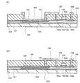
図1(A)は、支持基板100上に、イットリウム酸化物を含む、もしくはYSZを含む保持容量部絶縁層101と、保持容量部下部電極102と、配線103が形成されている。配線103は、保持容量部上部電極も兼ねている。保持容量部下部電極102が保持容量部絶縁層101に接する部分と、前記保持容量部絶縁層101が配線103に接する部分が、支持基板の上方からみて重なっている部分が保持容量部104となる。また同じ支持基板100に、TFT105が形成される。このTFT105は、結晶性シリコン層を活性層106とする。すなわち保持容量部下部電極102が保持容量部絶縁層101に接する面と、前記保持容量部絶縁層101が配線103に接する面は、一致する。尚、本明細書において一致とは、概略一致を含む。
In FIG. 1A, a storage capacitor
図1(A)の配線103は、TFTのソース領域及びドレイン領域と電気的に接続し、かつ保持容量部絶縁層101に接しているが、回路の設計上かならずしも一つの配線103が両条件を満たす必要はない。
The
一方、図1(B)は、図1(A)と似ているものの、保持容量部絶縁層101に接して、シリコン層からなる保持容量部上部電極107が形成されている。さらに、前記保持容量部上部電極107は、配線108と接続されている。このとき、保持容量部絶縁層101と保持容量部下部電極102とが接している部分と、保持容量部絶縁層101と前記保持容量部上部電極107とが接している部分が、支持基板の上方からみて重なっている部分が保持容量部104となる。
On the other hand, FIG. 1B is similar to FIG. 1A, but a storage capacitor portion
図1(B)の配線108は、TFTのソース領域及びドレイン領域として機能する高濃度不純物領域144a、144bと電気的に接続し、かつ保持容量部上部電極107とに電気的に接続しているが、回路の設計上かならずしも一つの配線108が両方に接続する必要はない。
The
本発明に用いる支持基板100の材料としては400℃以上の耐熱性があるものが望ましい。なぜなら前記結晶性シリコン層を支持基板へ接合する工程にて、400℃以上600℃以下の熱処理がされるからである。
As the material of the
支持基板100は絶縁性を有するものまたは絶縁表面を有するものであり、アルミノシリケートガラス、アルミノホウケイ酸ガラス、バリウムホウケイ酸ガラスのような電子工業用に使われるガラス基板(「無アルカリガラス基板」とも呼ばれる)が適用される。
The supporting
すなわち、支持基板100として、熱膨張係数が25×10−7/℃以上50×10−7/℃以下(好ましくは、30×10−7/℃から40×10−7/℃)であって歪み点が580℃から680℃(好ましくは、600℃から680℃)のガラス基板を適用することができる。その他に石英基板、セラミック基板、表面が絶縁膜で被覆された金属基板などのも適用可能である。
That is, the
TFTの活性層106は、単結晶シリコン基板を薄片化して形成されるものであり、すなわちLTSS層(Low Temperature Single crystal Semiconductor)から形成される。例えば、単結晶半導体基板として単結晶シリコン基板を用いた場合、単結晶シリコン基板の所定の深さに水素またはフッ素が添加されるようイオン照射し、その後熱処理を行って表層の単結晶シリコン層を剥離する方法で形成することができる。また、ポーラスシリコン(多孔性シリコン)上に単結晶シリコンをエピタキシャル成長させた後、ポーラスシリコン層をウォータージェットで劈開して剥離する方法を適用しても良い。LTSS層の厚さは5nm以上500nm以下、好ましくは10nm以上200nm以下の厚さである。
The
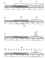
図1(A)に示すSOI構造を有する基板の作製方法について、図2(A)〜図2(D)、図3(A)〜図3(D)、図4(A)〜図4(D)、図5(A)〜図5(C)、を用いて説明する。 2A to 2D, FIGS. 3A to 3D, and FIGS. 4A to 4D are diagrams illustrating a method for manufacturing a substrate having an SOI structure illustrated in FIG. D) and FIGS. 5A to 5C will be described.
まず単結晶シリコン基板110の表面に、イットリウム酸化物を含む絶縁層、もしくはイットリウム酸化物とジルコニウム酸化物とを含む絶縁層を形成する。ここではYSZ膜111を成膜する。ターゲットはイットリウム酸化物を92mol%、ジルコニウム酸化物を8mol%にて混合したものを用いて、スパッタ法にて、成膜ガスをアルゴン(Ar)及び酸素(O2)、成膜圧力0.4Paとして、10nm以上200nm以下、ここでは50nmの膜厚で成膜する(図2(A)参照)。尚、前記成膜時の基板温度は高いほど良いが、本発明においては基板温度が室温でも良い。また上記ターゲットに他の添加物が入っていても、結晶性が損なわれなければ本発明の目的は達成される。
First, an insulating layer containing yttrium oxide or an insulating layer containing yttrium oxide and zirconium oxide is formed on the surface of the single
また、上記ではスパッタ法にて成膜しているが、CVD法でも良い。CVD成膜の例としてはジルコニウムおよびイットリウムのDPM錯体を原料とするものが挙げられる。 In the above, the film is formed by the sputtering method, but the CVD method may be used. An example of CVD film formation is one using a DPM complex of zirconium and yttrium as a raw material.
イットリウム酸化物、もしくはYSZは、耐熱性、化学的安定性に優れ、また結晶性シリコンを下地としたとき、特定の面方位に結晶成長しやすい特徴がある。また結晶性シリコンには、表面に非結晶状態の自然酸化膜が形成されるが、イットリウム酸化物、もしくはYSZの前記結晶成長はこれに影響されにくい。また、YSZは熱処理により比誘電率が高くなる特徴がある。 Yttrium oxide or YSZ is excellent in heat resistance and chemical stability, and has a characteristic that crystals are likely to grow in a specific plane orientation when crystalline silicon is used as a base. A crystalline silicon has a non-crystalline natural oxide film formed on its surface, but the crystal growth of yttrium oxide or YSZ is not easily affected by this. Further, YSZ has a feature that the relative dielectric constant is increased by heat treatment.
単結晶シリコンを基板として前記保持容量部の絶縁膜を成膜し熱処理する工程、その後、前記保持容量部の絶縁膜を結晶性シリコン層と共に支持基板すなわちガラス基板に接合する工程、という順にて進める必要がある。なぜなら、前記イットリウム酸化物、もしくはYSZの前記結晶成長は、750℃以上の熱処理が必要だからである。 A step of forming an insulating film of the storage capacitor portion using single crystal silicon as a substrate and performing a heat treatment, and then a step of bonding the insulating film of the storage capacitor portion together with a crystalline silicon layer to a supporting substrate, that is, a glass substrate. There is a need. This is because the crystal growth of the yttrium oxide or YSZ requires heat treatment at 750 ° C. or higher.
さらに、750℃以上1400℃以下の範囲、好ましくは850℃以上950℃以下の範囲にて加熱処理することにより、YSZ膜111は結晶化し、比誘電率が向上する。生産性、膜特性を考慮し、ここでは900℃で1hr熱処理する。
Further, by performing heat treatment in the range of 750 ° C. to 1400 ° C., preferably in the range of 850 ° C. to 950 ° C., the
その後、清浄化された単結晶シリコン基板110の表面から電界で加速されたイオン112を所定の深さに添加されるようイオン照射して脆化層113を形成する(図2(B)参照)。単結晶シリコン基板110に形成される脆化層113の深さは、イオンの加速エネルギーとイオンの入射角によって制御する。単結晶シリコン基板110の表面からイオンの平均進入深さに近い深さ領域に脆化層113が形成される。例えば、LTSS層の厚さは5nm以上500nm以下、好ましくは10nm以上200nm以下の厚さであり、イオンを照射する際の加速電圧はこのような厚さを考慮して行われる。イオンの照射はイオンドーピング装置を用いて行うことが好ましい。すなわち、原料ガスをプラズマ化して生成された複数のイオン(イオン種)を質量分離しないで照射するドーピング方式を用いる。
After that, the embrittled
本発明を実施するための最良の形態の場合、一または複数の同一の原子から成る質量数の異なるイオンを照射することが好ましい。イオンドーピングは、加速電圧10keVから100keV、好ましくは30keVから80keV、ドーズ量は1×10⁸/cm2から4×108/cm2、ビーム電流密度が2μA/cm2以上、好ましくは5μA/cm2以上、より好ましくは10μA/cm2以上とすれば良い。 In the best mode for carrying out the present invention, it is preferable to irradiate ions having one or more identical atoms and having different mass numbers. In the ion doping, an acceleration voltage of 10 keV to 100 keV, preferably 30 keV to 80 keV, a dose amount of 1 × 10 8 / cm 2 to 4 × 10 8 / cm 2 , and a beam current density of 2 μA / cm 2 or more, preferably 5 μA / cm It may be 2 or more, more preferably 10 μA / cm 2 or more.
水素イオンを照射する場合には、H+、H2 +、H3 +イオンを含ませると共に、H3 +イオンの割合を高めておくことが好ましい。水素イオンを照射する場合には、H+、H2 +、H3 +イオンを含ませると共に、H3 +イオンの割合を高めておくと照射効率を高めることができ、照射時間を短縮することができる。それにより、単結晶シリコン基板110に形成される脆化層113の領域には1×10²⁰/cm3(好ましくは5×1020/cm3)以上の水素を含ませることが可能である。
In the case of irradiation with hydrogen ions, it is preferable to include H + , H 2 + , and H 3 + ions and to increase the ratio of H 3 + ions. In the case of irradiation with hydrogen ions, H + , H 2 + , H 3 + ions are included, and if the ratio of H 3 + ions is increased, the irradiation efficiency can be increased and the irradiation time can be shortened. Can do. Accordingly, hydrogen of 1 × 10 20 / cm 3 (preferably 5 × 10 20 / cm 3 ) or more can be contained in the region of the
単結晶シリコン基板110中において、局所的に高濃度の水素照射領域を形成すると、結晶構造が乱されて微小な空孔が形成され、脆化層113を多孔質構造とすることができる。この場合、比較的低温の熱処理によって脆化層113に形成された微小な空洞の体積変化が起こり、脆化層113に沿って劈開することにより薄いLTSS層を形成することができる。
When a high-concentration hydrogen irradiation region is locally formed in the single
イオンを質量分離して単結晶シリコン基板110に照射しても、上記と同様に脆化層113を形成することができる。この場合にも、質量数の大きいイオン(例えばH3 +イオン)を選択的に照射することは上記と同様な効果を奏することとなり好ましい。
The
イオンを生成する生成するガスとしては水素の他に重水素を選択することも可能である。このようなイオンを単結晶シリコン基板110に照射することで、微小な空孔を形成することができ上記と同様な脆化層113を単結晶シリコン基板110中に設けることができる。
In addition to hydrogen, deuterium can also be selected as a gas that generates ions. By irradiating the single
脆化層113の形成に当たってはイオンを高ドーズ条件で照射する必要があり、単結晶シリコン基板110の表面が粗くなってしまう場合がある。そのためイオンが照射される表面に緻密な膜を設けておいても良い。例えば、窒化シリコン膜もしく酸素を含むは窒化シリコン膜などによりイオン照射に対する保護膜を50nm以上200nm以下の厚さで設けておいても良い。
In formation of the
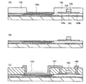
次いでYSZ膜111を選択的に除去して、保持容量部絶縁層101を所望の形状に形成する(図2(C)参照)。前記形状に形成する方法としては、希ガスあるいはハロゲンを用いてドライエッチングする例が挙げられる。他の方法としては、化学的機械的研磨(Chemical Mechanical Polishing:CMP)を用いるものが挙げられる。この場合、予め単結晶シリコン基板110の表面に酸化珪素膜を形成し、保持容量部絶縁層101を形成したい部分を選択的に除去し、YSZ膜111を成膜後にCMPにて加工する方法をとる。
Next, the
次いでタングステン(W)、モリブデン(Mo)、チタン、もしくはこれらを含む材料からなる保持容量部下部電極102を形成する(図2(C)参照)。この場合も、スパッタ成膜、およびハロゲン元素を加えたガスを用いてドライエッチングにて選択的に除去する。この保持容量部下部電極102と保持容量部絶縁層101とが重なる部分と、保持容量部絶縁層101と後の工程で形成される保持容量部の上部電極と重なる部分とが、概略一致する形状であれば、支持基板上に保持容量を効果的に配置することができる。
Next, a storage capacitor portion
前記保持容量部絶縁層101を所望の形状に形成する工程、及び保持容量部下部電極102を形成する工程は、脆化層113を形成する工程の後に行う。なぜなら、脆化層113を形成する工程にてイオンを所定の深さに照射する際、表面から均一の深さに添加するためには、表面が一様でなければならないからである。
The step of forming the storage capacitor
次いで絶縁膜114を形成する(図2(D)参照)。前記絶縁膜114として、窒素を含む酸化珪素膜を膜厚100nmで成膜し、さらに酸素を含む窒化珪素膜を膜厚300nmで成膜した積層膜を形成する。
Next, an insulating
さらに絶縁膜114を、CMPを用いて研磨し、表面が平滑な絶縁膜121を得る(図3(A)参照)。絶縁膜114は、その下に保持容量部下部電極102が形成されているので、段差が存在しているが、研磨によって段差を消失させる。
Further, the insulating
次に、単結晶シリコン基板110の支持基板100と接合を形成する面に接合層122を形成する(図3(B)参照)。接合層122は平滑面を有する層、あるいは親水性表面を有する層、あるいは平滑面と親水性表面とを有する層とする。このような表面を形成可能なものとして、化学的な反応により形成される絶縁層が好ましい。例えば、熱的または化学的な反応により形成される酸化半導体膜が適している。主として化学的な反応により形成される膜であれば表面の平滑性を確保できるからである。
Next, a
接合層122の下層が平滑な場合、親水性を確保するための膜厚の下限は1nmである。接合層122の下層に凹凸があれば接合層を厚くすることで平坦性を確保できるが、接合層122が厚すぎると接合層122自体に凹凸が生じる。そのため接合層122は1nm以上500nm以下の厚さで設けられる。
When the lower layer of the
接合層122としてケミカルオキサイドを用いる場合には1nmから10nmの厚さであれば良い。また、好適には化学気相成長法により堆積される酸化シリコンを接合層122とすることができる。この場合、有機シランガスを用いて化学気相成長法により作製される酸化シリコン膜が好ましい。
When chemical oxide is used as the
有機シランガスとしては、珪酸エチル(TEOS:化学式Si(OC2H5)4)、テトラメチルシラン(TMS:化学式Si(CH3)4)、テトラメチルシクロテトラシロキサン(TMCTS)、オクタメチルシクロテトラシロキサン(OMCTS)、ヘキサメチルジシラザン(HMDS)、トリエトキシシラン(SiH(OC2H5)3)、トリスジメチルアミノシラン(SiH(N(CH3)2)3)等のシリコン含有化合物を用いることができる。 Examples of the organic silane gas include ethyl silicate (TEOS: chemical formula Si (OC 2 H 5 ) 4 ), tetramethylsilane (TMS: chemical formula Si (CH 3 ) 4 ), tetramethylcyclotetrasiloxane (TMCTS), and octamethylcyclotetrasiloxane. It is possible to use a silicon-containing compound such as (OMCTS), hexamethyldisilazane (HMDS), triethoxysilane (SiH (OC 2 H 5 ) 3 ), trisdimethylaminosilane (SiH (N (CH 3 ) 2 ) 3 ). it can.
単結晶シリコン基板110の支持基板100と接合を形成する面に設けられた接合層122は、支持基板100の表面と密接することで、室温であっても接合をすることが可能である。異種材料である支持基板100と接合層122を接合するには表面を清浄化する。支持基板100と接合層122の互いに清浄化された表面を密接させると表面間引力により接合が形成される(図3(C)参照)。
The
さらに、支持基板100の表面に複数の親水基を付着させる処理を加えると、接合を形成するのにより好ましい態様となる。例えば、支持基板100の表面を酸素プラズマ処理もしくはオゾン処理して親水性にすることが好ましい。
Further, when a treatment for attaching a plurality of hydrophilic groups to the surface of the
このように支持基板100の表面を親水性にする処理を加えた場合には、表面の水酸基が作用して水素結合により接合が形成される。さらに清浄化された表面同士を密接させて接合を形成したものに対して、室温以上の温度で加熱すると接合強度を高めることができる。
Thus, when the process which makes the surface of the
良好な接合を形成するために、表面を活性化しておいても良い。例えば、接合を形成する面に原子ビームもしくはイオンビームを照射する。原子ビームもしくはイオンビームを利用する場合には、アルゴン等の不活性ガス中性原子ビームもしくは不活性ガスイオンビームを用いることができる。その他に、プラズマ照射もしくはラジカル処理を行う。このような表面処理により200℃以上400℃以下の温度であっても異種材料間の接合強度を高めることが可能となる。 In order to form a good bond, the surface may be activated. For example, the surface on which the junction is formed is irradiated with an atomic beam or an ion beam. When an atomic beam or an ion beam is used, an inert gas neutral atom beam or inert gas ion beam such as argon can be used. In addition, plasma irradiation or radical treatment is performed. Such surface treatment makes it possible to increase the bonding strength between different kinds of materials even at a temperature of 200 ° C. or higher and 400 ° C. or lower.
単結晶シリコン基板110と支持基板100を重ね合わせた状態で第1の熱処理を行う。第1の熱処理により支持基板100上に薄いシリコン層(LTSS層)を残して単結晶シリコン基板110の分離を行う。第1の熱処理は接合層122の成膜温度以上で行うことが好ましく、400℃以上600℃未満の温度で行うことが好ましい。この温度範囲で熱処理を行うことで脆化層113に形成された微小な空孔に体積変化が起こり、単結晶シリコン基板110と支持基板100とを脆化層113にて分離することができる。接合層122は支持基板100と接合しているので、支持基板100上には単結晶シリコン基板110と同じ結晶性のLTSS層123が固定された形態となる(図3(D)参照)。
First heat treatment is performed in a state where the single
次に支持基板100にLTSS層が接合された状態で第2の熱処理を行う。第2の熱処理は、第1の熱処理温度よりも高い温度であって支持基板100の歪み点を超えない温度で行うことが好ましい。或いは、第1の熱処理と第2の熱処理は同じ温度であっても、第2の熱処理の処理時間を長くすることが好ましい。熱処理は、熱伝導加熱、対流加熱または輻射加熱などにより支持基板100及び/またはLTSS層123が加熱されるようにすれば良い。熱処理装置としては電熱炉、ランプアニール炉などを適用することができる。第2の熱処理は多段階に温度を変化させて行っても良い。また瞬間熱アニール(RTA)装置を用いても良い。RTA装置によって熱処理を行う場合には、基板の歪み点近傍またはそれよりも若干高い温度に加熱することもできる。
Next, second heat treatment is performed in a state where the LTSS layer is bonded to the
第2の熱処理を行うことでLTSS層123に残留する応力を緩和することができる。すなわち、第2の熱処理は、支持基板100とLTSS層123の膨張係数の違いにより生じる熱歪みを緩和する。また、第2の熱処理は、イオンを照射することによって結晶性が損なわれたLTSS層123の結晶性を回復させるためにも有効である。さらに、第2の熱処理は、単結晶シリコン基板110を支持基板100と接合させた後、第1の熱処理によって分割する際に生じるLTSS層123のダメージを回復させることにも有効である。また、第1の熱処理と第2の熱処理を行うことで水素結合を、より強固な共有結合に変化させることができる。
By performing the second heat treatment, the stress remaining in the
LTSS層123の表面をより平坦化する目的で化学的機械研磨(CMP)処理を行っても良い。CMP処理は第1の熱処理後もしくは第2の熱処理後に行うことができる。尤も、第2の熱処理前に行えば、LTSS層123の表面を平坦化すると共にCMP処理によって生じる表面の損傷層を第2の熱処理で修復することができる。
Chemical mechanical polishing (CMP) treatment may be performed for the purpose of further flattening the surface of the
いずれにしても、第1の熱処理と第2の熱処理を本形態のように組み合わせて行うことで、ガラス基板のような熱的に脆弱な支持基板の上に、結晶性に優れた結晶シリコン層を設けることが可能となる。 In any case, a crystalline silicon layer having excellent crystallinity is formed on a thermally fragile supporting substrate such as a glass substrate by combining the first heat treatment and the second heat treatment as in this embodiment. Can be provided.
次いでLTSS層123を薄膜化して所望の膜厚のLTSS層124を形成する(図3(E)参照)。薄膜化の方法は、CMP法、あるいはエッチング法等が挙げられる。本発明を実施するための最良の形態では、ドライエッチングを用いて薄膜化する。
Next, the
LTSS層124の膜厚は5nmから500nm、好ましくは10nmから200nm、より好ましくは10nmから60nmの厚さとすることが好ましい。LTSS層124の厚さは、脆化層113の深さを制御すること、及び薄膜化の条件により適宜設定できる。本発明を実施するための最良の形態では、ドライエッチングにより、LTSS層124を50nmの膜厚に形成する。
The thickness of the
LTSS層124にはしきい値電圧を制御するために、ホウ素、アルミニウム、ガリウムなどのp型不純物元素を添加する。例えば、p型不純物元素としてホウ素を1×1016cm−3以上1×1018cm−3以下の濃度で添加されていても良い。
A p-type impurity element such as boron, aluminum, or gallium is added to the
LTSS層124上にマスク131を形成し、マスク131を用いてLTSS層124をエッチングする(図4(A)参照)。活性層の配置に合わせて島状に分離した島状単結晶シリコン層133及び保持容量部絶縁層101の保護層109を形成する(図4(B)参照)。
A
上記の工程で形成された保持容量部下部電極102と保護層109は、互いに接触しないよう形成する。保護層は単結晶シリコンで形成されることから、保護層加工時にエッチング残りがあった場合、上部電極と下部電極が接触し電荷を逃がすことを防ぐためである。
The storage capacitor portion
そして、島状単結晶シリコン層133上に、ゲート絶縁膜134、ゲート電極135を形成する(図4(C)参照)。本発明を実施するための最良の形態では、ゲート絶縁膜134とゲート電極135を同じ幅にしたが、低濃度不純物領域を形成するために、ゲート電極135の幅よりも大きくしてもよい。
Then, a
ゲート絶縁膜134は、酸化珪素膜、窒化珪素膜、窒素を含む酸化珪素膜、酸素を含む窒化珪素膜のいずれかを用いて形成すればよく、本発明を実施するための最良の形態では、酸化珪素膜を10nm以上100nm以下の膜厚で成膜したものを用いて、ゲート絶縁膜134を形成する。
The
ゲート電極135は、タングステン(W)、タンタル(Ta)、チタン(Ti)、アルミニウム(Al)、もしくはそれらの窒化物、もしくはその組み合わせ等を用いて形成すればよい。
The
次いで、ゲート電極135をマスクとして、島状単結晶シリコン層133に一導電型を付与する不純物元素136を導入する(図4(D)参照)。このとき保護層109にも不純物元素136が添加される。不純物元素136としてn型を付与する不純物元素を用いた場合は、n型を付与する不純物元素として、リン(P)、ヒ素(As)が挙げられる。また不純物元素136としてp型を付与する不純物元素を用いた場合は、p型を付与する不純物元素としては、ホウ素(B)が挙げられる。
Next, an
一導電型を付与する不純物元素136の添加により、ゲート電極135の下の領域にチャネル形成領域143、ゲート電極135及びゲート絶縁膜134に覆われていない領域に、ソース領域及びドレイン領域である高濃度不純物領域144a、144b、及び高濃度不純物領域144cが形成される(図5(A)参照)。
By the addition of the
本発明を実施するための最良の形態では、例えばn型の不純物元素136としてリン(P)を添加する。これにより高濃度不純物領域144a〜144cには、リンが1×10¹⁹atoms/cm3以上1×1021atoms/cm3以下(代表的には1×1020atoms/cm3以上5×1020atoms/cm3以下)の濃度で含まれることとなる。
In the best mode for carrying out the present invention, for example, phosphorus (P) is added as the n-
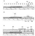
次いで保持容量部絶縁層101上の保護層109以外を覆うマスク142を形成し、高濃度不純物領域144cをエッチングして除去し、保持容量部絶縁層101を露出させる(図5(B)参照)。
Next, a
図5(B)までの作製工程を行った後、層間絶縁膜145を形成する。層間絶縁膜145はBPSG(Boron Phosphorus Silicon Glass)膜を成膜するか、ポリイミドに代表される有機樹脂を塗布して形成する。層間絶縁膜145中に開口部を形成し、配線146及び配線147を形成する(図5(C)参照)。なお、配線147は、図1(A)の配線103に相当する。
After the manufacturing steps up to FIG. 5B are performed, an
配線146及び配線147は、活性層である島状単結晶シリコン層133及び保持容量部絶縁層101と接触抵抗の低い材料を用いて形成すればよい。本発明を実施するための最良の形態では、配線146及び配線147をアルミニウムもしくはアルミニウム合金で形成する。また上層と下層にはバリアメタルとしてモリブデン、クロム、チタンなどの金属膜で形成してもよい。
The
また配線146は高濃度不純物領域144bと電気的に接続されており、配線147は高濃度不純物領域144aと電気的に接続し保持容量部絶縁層101と一部重なっている。前記配線147と、保持容量部絶縁層101と、容量部下部電極102が重なった部分が、保持容量部104を形成する。
The
以上、図1(A)の作製工程について説明したが、以下に図1(B)の作製工程、すなわち前記保護層109を除去せず、保持容量部の上部電極として用いる構造の作製方法について図6(A)〜図6(C)を用いて説明する。なお図6(A)〜図6(C)において、図5(A)〜図5(C)と同じものは同じ符号で示している。
Although the manufacturing process of FIG. 1A has been described above, the manufacturing process of FIG. 1B, that is, a manufacturing method of a structure used as an upper electrode of a storage capacitor portion without removing the
まず、図3(A)〜図4(C)で説明した作製方法により、島状単結晶シリコン層133上に、ゲート絶縁膜134、ゲート電極135を設けるところまで作製する。図4(D)の工程同様、ゲート電極135をマスクとして、島状単結晶シリコン層133に一導電型を付与する不純物元素136を導入する(図6(A)参照)。このとき保護層109にも不純物元素136が添加される。この保護層109の、保持容量部絶縁層101と一部重なっている部分は高濃度不純物領域144cになり、保持容量部上部電極としての機能をもつ。高濃度不純物領域144cは十分抵抗が低くなれば良く、一例ではリンが1×10²⁰atoms/cm3以上1×1021atoms/cm3以下の濃度で含まれればよい。
First, a
その後、層間絶縁膜152を形成する。層間絶縁膜152はBPSG(Boron Phosphorus Silicon Glass)膜を成膜するか、ポリイミドに代表される有機樹脂を塗布して形成する。層間絶縁膜152中に開口部を形成し、配線146及び配線153を形成する(図6(C)参照)。なお、配線153は、図1(B)配線108に相当する。
Thereafter, an
配線146及び配線153は、活性層である島状単結晶シリコン層133及び保持容量部上部電極として機能する高濃度不純物領域144cと接触抵抗の低い材料を用いて形成すればよい。
The
また配線146は高濃度不純物領域144bと電気的に接続されており、配線153は高濃度不純物領域144aと電気的に接続し保持容量部絶縁層101と一部重なっている。高濃度不純物領域144cと、保持容量部絶縁層101と、保持容量部下部電極102が重なった部分が、保持容量部104になる。
The
図1(A)及び図5(C)の構造を得るために、高濃度不純物領域144cをプラズマエッチングする際、保持容量部絶縁層101の膜厚が減る、もしくは保持容量部絶縁層101自体にダメージを受け非結晶化する可能性がある。そこで、保持容量部の電極として図5(C)に示す配線147(図1(A)配線103に相当する)を用いることにより、電極の抵抗が小さく高速動作が可能となる点で有利となる。また図1(B)及び図6(C)の構造を得るためには、保持容量部の電極として高濃度不純物領域144c(図1(A)保持容量部上部電極107に相当する)を用いており、この高濃度不純物領域144cは図5(C)の配線147より抵抗が高いため、容量としての動作速度は小さくなる。図5(A)に示すような高濃度不純物領域144cをプラズマエッチングするためのマスク142が不要になるため、工程数を減らすことができ、さらに保持容量部絶縁層101の膜厚が減ることがなく、また保持容量部絶縁層101がプラズマに曝されない点で有利となる。このように、本実施の形態を選択することにより、動作速度の向上と、生産性の向上と、のいずれかをより好適に達成することが出来る。
In order to obtain the structures of FIGS. 1A and 5C, when the high-
以上により、比誘電率の高いYSZ膜を保持容量部に用いることで、駆動速度が速く、信頼性の高い半導体装置を得ることができる。また同様の理由で、保持容量部の面積を小さくすることができる。 As described above, by using a YSZ film having a high relative dielectric constant for the storage capacitor portion, a semiconductor device with high driving speed and high reliability can be obtained. For the same reason, the area of the storage capacitor portion can be reduced.
本発明を実施するための最良の形態によれば、ガラス基板等の耐熱温度が750℃未満の支持基板100であっても接合部の接着力が強固なLTSS層を得ることができる。支持基板100として、アルミノシリケートガラス、アルミノホウケイ酸ガラス、バリウムホウケイ酸ガラスの如き無アルカリガラスと呼ばれる電子工業用に使われる各種ガラス基板を適用することが可能となる。すなわち、一辺が1メートルを超える基板上に単結晶シリコン層を形成することができる。このような大面積基板を使って液晶ディスプレイのような表示装置のみならず、半導体集積回路を製造することができる。
According to the best mode for carrying out the present invention, it is possible to obtain an LTSS layer having a strong bonding strength at the joint even if the supporting
(実施の形態2)
本実施の形態では、SOI基板及びTFTを組み込んだ半導体装置について、図7及び図8を用いて説明する。
(Embodiment 2)
In this embodiment, a semiconductor device incorporating an SOI substrate and a TFT will be described with reference to FIGS.
図7では半導体装置の一例として、マイクロプロセッサ200を示す。このマイクロプロセッサ200は、演算回路201(Arithmetic logic unit;ALUともいう)、演算回路制御部202(ALU Controller)、命令解析部203(Instruction Decoder)、割り込み制御部204(Interrupt Controller)、タイミング制御部205(Timing Controller)、レジスタ206(Register)、レジスタ制御部207(Register Controller)、バスインターフェース208(Bus I/F)、ROM209(Read Only Memory:読み出し専用メモリ)、及びROMインターフェース210(ROM I/F)を有している。
FIG. 7 illustrates a
バスインターフェース208を介してマイクロプロセッサ200に入力された命令は命令解析部203に入力され、デコードされた後に演算回路制御部202、割り込み制御部204、レジスタ制御部207、タイミング制御部205に入力される。演算回路制御部202、割り込み制御部204、レジスタ制御部207、タイミング制御部205は、デコードされた命令に基づき各種制御を行う。具体的に演算回路制御部202は、演算回路201の動作を制御するための信号を生成する。
An instruction input to the
また、割り込み制御部204は、マイクロプロセッサ200のプログラム実行中に、外部の入出力装置や周辺回路からの割り込み要求を、その優先度やマスク状態から判断して処理する。レジスタ制御部207は、レジスタ206のアドレスを生成し、マイクロプロセッサ200の状態に応じてレジスタ206の読み出しや書き込みを行う。タイミング制御部205は、演算回路201、演算回路制御部202、命令解析部203、割り込み制御部204、レジスタ制御部207の動作のタイミングを制御する信号を生成する。例えばタイミング制御部205は、基準クロック信号CLK1を元に、内部クロック信号CLK2を生成する内部クロック生成部を備えており、クロック信号CLK2を上記各種回路に供給する。
The interrupt control unit 204 processes an interrupt request from an external input / output device or a peripheral circuit based on its priority or mask state during execution of the program of the
なお、図7に示すマイクロプロセッサ200は、その構成を簡略化して示した一例にすぎず、実際にはその用途によって多種多様な構成を備えることができる。
Note that the
このようなマイクロプロセッサ200は、支持基板に接合された結晶方位が一定の単結晶シリコン層(LTSS層)を有するTFTにより集積回路が形成されているので、処理速度の高速化を図ることができる。また、高い比誘電率のYSZ膜を用いることで保持容量の電極面積を小さくしているので、素子全体の縮小化が出来る。
In such a
次に、非接触でデータの送受信を行うことのできる演算機能を備えた半導体装置の一例について、図8を参照して説明する。 Next, an example of a semiconductor device having an arithmetic function capable of transmitting and receiving data without contact will be described with reference to FIGS.
図8は無線通信により外部装置と信号の送受信を行って動作するコンピュータ(以下、「RFCPU」という)の一例を示す。RFCPU211は、アナログ回路部212とデジタル回路部213を有している。アナログ回路部212として、共振容量を有する共振回路214、整流回路215、定電圧回路216、リセット回路217、発振回路218、復調回路219と、変調回路220を有している。デジタル回路部213は、RFインターフェース221、制御レジスタ222、クロックコントローラ223、CPUインターフェース224、CPU225(Central Processing Unit:中央処理ユニット)、RAM226(Random Access Memory:ランダムアクセスメモリ)、ROM227(Read Only Memory:読み出し専用メモリ)を有している。
FIG. 8 shows an example of a computer (hereinafter referred to as “RFCPU”) that operates by transmitting and receiving signals to and from an external device by wireless communication. The
このような構成のRFCPU211の動作は以下の通りである。アンテナ228が受信した信号は共振回路214により誘導起電力を生じる。誘導起電力は整流回路215を経て容量部229に充電される。この容量部229はセラミックコンデンサーや電気二重層コンデンサーなどのキャパシタで形成されていることが好ましい。
The operation of the
容量部229は本発明の作製方法で形成されたYSZ膜を用いることができるが、RFCPU211と一体形成されている必要はなく、別部品としてRFCPU211を構成する絶縁表面を有する基板に取り付けられていれば良い。
As the
リセット回路217は、デジタル回路部213をリセットし初期化する信号を生成する。例えば、電源電圧の上昇に遅延して立ち上がる信号をリセット信号として生成する。発振回路218は定電圧回路216により生成される制御信号に応じて、クロック信号の周波数とデューティ比を変更する。ローパスフィルタで形成される復調回路219は、例えば振幅変調(ASK)方式の受信信号の振幅の変動を二値化する。
The
変調回路220は、送信データを振幅変調(ASK)方式の送信信号の振幅を変動させて送信する。変調回路220は、共振回路214の共振点を変化させることで通信信号の振幅を変化させている。クロックコントローラ223は、電源電圧又はCPU225における消費電流に応じてクロック信号の周波数とデューティ比を変更するための制御信号を生成している。電源電圧の監視は電源管理回路230が行っている。
The
アンテナ228からRFCPU211に入力された信号は復調回路219で復調された後、RFインターフェース221で制御コマンドやデータなどに分解される。制御コマンドは制御レジスタ222に格納される。制御コマンドには、ROM227に記憶されているデータの読み出し、RAM226へのデータの書き込み、CPU225への演算命令などが含まれている。
A signal input from the
CPU225は、CPUインターフェース224を介してROM227、RAM226、制御レジスタ222にアクセスする。CPUインターフェース224は、CPU225が要求するアドレスより、ROM227、RAM226、制御レジスタ222のいずれかに対するアクセス信号を生成する機能を有している。
The
CPU225の演算方式は、ROM227にOS(オペレーティングシステム)を記憶させておき、起動とともにプログラムを読み出し実行する方式を採用することができる。また、専用回路で演算回路を構成して、演算処理をハードウェア的に処理する方式を採用することもできる。ハードウェアとソフトウェアを併用する方式では、専用の演算回路で一部の処理を行い、残りの演算はプログラムを使ってCPU225が実行する方式を適用することができる。
As a calculation method of the
このようなRFCPU211は、絶縁表面接合された結晶方位が一定の単結晶シリコン層(LTSS層)が形成されているので、処理速度の高速化を図ることができる。また、高い比誘電率のYSZ膜を用いることで保持容量の電極面積を小さくしているので、素子全体の縮小化が出来る。
In such an
図8ではRFCPUの形態について示しているが、通信機能、演算処理機能、メモリ機能を備えたものであれば、ICタグのようなものであっても良い。 Although FIG. 8 shows the form of the RFCPU, an IC tag may be used as long as it has a communication function, an arithmetic processing function, and a memory function.
100 支持基板
101 保持容量部絶縁層
102 保持容量部下部電極
103 配線
104 保持容量部
105 TFT
106 活性層
107 保持容量部上部電極
108 配線
109 保護層
110 単結晶シリコン基板
111 YSZ膜
112 イオン
113 脆化層
114 絶縁膜
121 絶縁膜
122 接合層
123 LTSS層
124 LTSS層
131 マスク
133 島状単結晶シリコン層
134 ゲート絶縁膜
135 ゲート電極
136 不純物元素
142 マスク
143 チャネル形成領域
144a 高濃度不純物領域
144b 高濃度不純物領域
144c 高濃度不純物領域
145 層間絶縁膜
146 配線
147 配線
152 層間絶縁膜
153 配線
200 マイクロプロセッサ
201 演算回路
202 演算回路制御部
203 命令解析部
204 制御部
205 タイミング制御部
206 レジスタ
207 レジスタ制御部
208 バスインターフェース
209 ROM
210 ROMインターフェース
211 RFCPU
212 アナログ回路部
213 デジタル回路部
214 共振回路
215 整流回路
216 定電圧回路
217 リセット回路
218 発振回路
219 復調回路
220 変調回路
221 RFインターフェース
222 制御レジスタ
223 クロックコントローラ
224 CPUインターフェース
225 CPU
226 RAM
227 ROM
228 アンテナ
229 容量部
230 電源管理回路
DESCRIPTION OF
106
210
212
226 RAM
227 ROM
Claims (4)
前記絶縁層に、熱処理を行って結晶化し、
水素を含むイオンを、前記絶縁層上より照射して、前記単結晶シリコン基板中に多孔質構造を有する脆化層を形成し、
前記絶縁層を島状に加工して保持容量部絶縁層を形成し、
前記単結晶シリコン基板上及び前記保持容量部絶縁層上に、保持容量部下部電極を形成し、
前記単結晶シリコン基板上、前記保持容量部絶縁層上及び前記保持容量部下部電極上に、第2の絶縁層を形成し、
前記第2の絶縁層上に、第1の絶縁層を形成し、
前記第1の絶縁層と支持基板とを貼りあわせた後、前記脆化層から前記単結晶シリコン基板の一部を分離することにより、
前記支持基板上に、
前記第1の絶縁層と、
前記第1の絶縁層上の前記第2の絶縁層と、
前記第2の絶縁層上の前記保持容量部下部電極と、
前記保持容量部下部電極上の前記保持容量部絶縁層と、
前記保持容量部絶縁層上及び前記第2の絶縁層上の、前記単結晶シリコン基板の一部である単結晶シリコン層と、を形成し、
前記単結晶シリコン層を島状に加工することにより、前記第2の絶縁層上に第1の島状単結晶シリコン層を形成するとともに、前記保持容量部絶縁層上に第2の島状単結晶シリコン層からなる保護層を形成し、
前記第1の島状単結晶シリコン層上に、ゲート絶縁膜及びゲート電極を形成し、
前記ゲート電極をマスクとして、前記第1の島状単結晶シリコン層に一導電型を付与する不純物元素を添加して、ソース領域及びドレイン領域を形成し、
前記保護層をエッチングして、前記保持容量部絶縁層の一部を露出させ、
前記第1の島状単結晶シリコン層、前記ゲート絶縁膜、前記ゲート電極を覆って、層間絶縁膜を形成し、
前記層間絶縁膜上に、前記ソース領域及び前記ドレイン領域の一方と電気的に接続し、
前記保持容量部絶縁層に接する配線を形成し、
前記配線の、前記保持容量部絶縁層に接する部分は、保持容量部上部電極となることを特徴とする半導体装置の作製方法。 An insulating layer containing yttrium oxide or an insulating layer containing yttrium oxide and zirconium oxide is formed over a single crystal silicon substrate,
Before Kize' edge layer, crystallized by heat treatment,
Ions containing hydrogen, is irradiated from the front Kize' edge layer, to form an embrittlement layer having a porous structure in the monocrystalline silicon substrate,
By processing the front Kize' edge layer in an island shape to form a storage capacitor portion insulating layer,
Forming a storage capacitor portion lower electrode on the single crystal silicon substrate and the storage capacitor portion insulating layer;
Forming a second insulating layer on the single crystal silicon substrate, on the storage capacitor portion insulating layer, and on the storage capacitor portion lower electrode;
Forming a first insulating layer on the second insulating layer;
After laminating the first insulating layer and the support substrate, by separating a part of the single crystal silicon substrate from the embrittlement layer ,
On the support substrate ,
The first insulating layer;
The second insulating layer on the first insulating layer;
The storage capacitor lower electrode on the second insulating layer;
The storage capacitor portion insulating layer on the storage capacitor portion lower electrode;
Forming a single crystal silicon layer that is a part of the single crystal silicon substrate on the storage capacitor portion insulating layer and the second insulating layer;
By processing the single crystal silicon layer into an island shape, a first island single crystal silicon layer is formed on the second insulating layer, and a second island shape single layer is formed on the storage capacitor portion insulating layer. Forming a protective layer consisting of a crystalline silicon layer ;
Forming a gate insulating film and a gate electrode on the first island-like single crystal silicon layer;
Said gate electrode as a mask, by adding an impurity element imparting one conductivity type in the first island-shaped single crystal silicon layer, forming a source region and a drain area,
Etching the protective layer to expose a part of the storage capacitor insulating layer,
Covering the first island-like single crystal silicon layer, the gate insulating film, and the gate electrode, forming an interlayer insulating film;
On the interlayer insulating film, electrically connected to one of the source region and the drain region ,
Forming a wiring in contact with the front Symbol storage capacitor portion insulating layer,
A method for manufacturing a semiconductor device , wherein a portion of the wiring in contact with the storage capacitor portion insulating layer serves as a storage capacitor portion upper electrode .
前記絶縁層に、熱処理を行って結晶化し、
水素を含むイオンを、前記絶縁層上より照射して、前記単結晶シリコン基板中に多孔質構造を有する脆化層を形成し、
前記絶縁層を島状に加工して保持容量部絶縁層を形成し、
前記シリコン基板上及び前記保持容量部絶縁層上に、保持容量部下部電極を形成し、前記シリコン基板上、前記保持容量部絶縁層上及び前記保持容量部下部電極上に、第2の絶縁層を形成し、
前記第2の絶縁層上に、第1の絶縁層を形成し、
前記第1の絶縁層と支持基板とを貼りあわせた後、前記脆化層から前記単結晶シリコン基板の一部を分離することにより、
前記支持基板上に、
前記第1の絶縁層と、
前記第1の絶縁層上の前記第2の絶縁層と、
前記第2の絶縁層上の前記保持容量部下部電極と、
前記保持容量部下部電極上の前記保持容量部絶縁層と、
前記保持容量部絶縁層上及び前記第2の絶縁層上の、前記単結晶シリコン基板の一部である単結晶シリコン層と、を形成し、
前記単結晶シリコン層を島状に加工することにより、前記第2の絶縁層上に第1の島状単結晶シリコン層を形成するとともに、前記保持容量部絶縁層上に第2の島状単結晶シリコン層を形成し、
前記第1の島状単結晶シリコン層上に、ゲート絶縁膜及びゲート電極を形成し、
前記ゲート電極をマスクとして、前記第1の島状単結晶シリコン層に一導電型を付与する不純物元素を添加して、ソース領域及びドレイン領域を形成するとともに、前記第2の島状単結晶シリコン層に一導電型を付与する不純物元素を添加して保持容量部上部電極を形成し、
前記第1の島状単結晶シリコン層、前記ゲート絶縁膜、前記ゲート電極、及び前記保持容量部上部電極を覆って、層間絶縁膜を形成し、
前記層間絶縁膜上に、前記ソース領域及び前記ドレイン領域の一方と、前記保持容量上部電極とを接続する配線を形成することを特徴とする半導体装置の作製方法。 An insulating layer containing yttrium oxide or an insulating layer containing yttrium oxide and zirconium oxide is formed over a single crystal silicon substrate,
Before Kize' edge layer, crystallized by heat treatment,
Ions containing hydrogen, is irradiated from the front Kize' edge layer, to form an embrittlement layer having a porous structure in the monocrystalline silicon substrate,
By processing the front Kize' edge layer in an island shape to form a storage capacitor portion insulating layer,
A storage capacitor unit lower electrode is formed on the silicon substrate and the storage capacitor unit insulating layer, and a second insulating layer is formed on the silicon substrate , the storage capacitor unit insulating layer, and the storage capacitor unit lower electrode. Form the
Forming a first insulating layer on the second insulating layer;
After laminating the first insulating layer and the support substrate, by separating a part of the single crystal silicon substrate from the embrittlement layer,
On the support substrate ,
The first insulating layer;
The second insulating layer on the first insulating layer;
The storage capacitor lower electrode on the second insulating layer;
The storage capacitor portion insulating layer on the storage capacitor portion lower electrode;
Forming a single crystal silicon layer that is a part of the single crystal silicon substrate on the storage capacitor portion insulating layer and the second insulating layer;
By processing the single crystal silicon layer in an island shape, the second on the insulating layer to form a first island-shaped single crystal silicon layer, the second island-like single in the storage capacitor portion insulating layer Forming a crystalline silicon layer,
Forming a gate insulating film and a gate electrode on the first island-like single crystal silicon layer;
Said gate electrode as a mask, by adding an impurity element imparting one conductivity type in the first island-shaped single crystal silicon layer, and forming a source region and a drain area, the second island-shaped single crystal An impurity element imparting one conductivity type is added to the silicon layer to form a storage capacitor portion upper electrode,
Covering the first island-shaped single crystal silicon layer, the gate insulating film, the gate electrode, and the storage capacitor portion upper electrode, an interlayer insulating film is formed,
A method for manufacturing a semiconductor device, comprising: forming a wiring connecting one of the source region and the drain region and the storage capacitor upper electrode over the interlayer insulating film.
Priority Applications (1)
| Application Number | Priority Date | Filing Date | Title |
|---|---|---|---|
| JP2008245254A JP5328276B2 (en) | 2007-09-27 | 2008-09-25 | Method for manufacturing semiconductor device |
Applications Claiming Priority (3)
| Application Number | Priority Date | Filing Date | Title |
|---|---|---|---|
| JP2007250356 | 2007-09-27 | ||
| JP2007250356 | 2007-09-27 | ||
| JP2008245254A JP5328276B2 (en) | 2007-09-27 | 2008-09-25 | Method for manufacturing semiconductor device |
Publications (3)
| Publication Number | Publication Date |
|---|---|
| JP2009099965A JP2009099965A (en) | 2009-05-07 |
| JP2009099965A5 JP2009099965A5 (en) | 2011-09-15 |
| JP5328276B2 true JP5328276B2 (en) | 2013-10-30 |
Family
ID=40507176
Family Applications (1)
| Application Number | Title | Priority Date | Filing Date |
|---|---|---|---|
| JP2008245254A Expired - Fee Related JP5328276B2 (en) | 2007-09-27 | 2008-09-25 | Method for manufacturing semiconductor device |
Country Status (2)
| Country | Link |
|---|---|
| US (2) | US8067793B2 (en) |
| JP (1) | JP5328276B2 (en) |
Families Citing this family (10)
| Publication number | Priority date | Publication date | Assignee | Title |
|---|---|---|---|---|
| JP5370100B2 (en) * | 2009-11-26 | 2013-12-18 | 株式会社村田製作所 | Method for manufacturing piezoelectric device |
| KR101473684B1 (en) | 2009-12-25 | 2014-12-18 | 가부시키가이샤 한도오따이 에네루기 켄큐쇼 | Semiconductor device |
| US20130170097A1 (en) * | 2011-06-29 | 2013-07-04 | Space Charge, LLC | Yttria-stabilized zirconia based capacitor |
| US10601074B2 (en) | 2011-06-29 | 2020-03-24 | Space Charge, LLC | Rugged, gel-free, lithium-free, high energy density solid-state electrochemical energy storage devices |
| US9853325B2 (en) | 2011-06-29 | 2017-12-26 | Space Charge, LLC | Rugged, gel-free, lithium-free, high energy density solid-state electrochemical energy storage devices |
| US11527774B2 (en) | 2011-06-29 | 2022-12-13 | Space Charge, LLC | Electrochemical energy storage devices |
| US8772130B2 (en) | 2011-08-23 | 2014-07-08 | Semiconductor Energy Laboratory Co., Ltd. | Manufacturing method of SOI substrate |
| US8969130B2 (en) | 2011-11-18 | 2015-03-03 | Semiconductor Energy Laboratory Co., Ltd. | Insulating film, formation method thereof, semiconductor device, and manufacturing method thereof |
| KR102304725B1 (en) * | 2014-10-16 | 2021-09-27 | 삼성디스플레이 주식회사 | Thin film transistor array substrate, method of manufacturing thereof and organic light-emitting display including the same |
| WO2019173626A1 (en) | 2018-03-07 | 2019-09-12 | Space Charge, LLC | Thin-film solid-state energy-storage devices |
Family Cites Families (20)
| Publication number | Priority date | Publication date | Assignee | Title |
|---|---|---|---|---|
| JPH05109629A (en) | 1991-10-16 | 1993-04-30 | Tonen Corp | Polycrystalline silicon thin film and its manufacturing method as well as thin-film transistor using thin film |
| JP3251778B2 (en) * | 1993-09-27 | 2002-01-28 | 三菱電機株式会社 | Semiconductor storage device and method of manufacturing the same |
| US5814529A (en) * | 1995-01-17 | 1998-09-29 | Semiconductor Energy Laboratory Co., Ltd. | Method for producing a semiconductor integrated circuit including a thin film transistor and a capacitor |
| JP3270674B2 (en) * | 1995-01-17 | 2002-04-02 | 株式会社半導体エネルギー研究所 | Manufacturing method of semiconductor integrated circuit |
| JP3286127B2 (en) * | 1995-08-14 | 2002-05-27 | ティーディーケイ株式会社 | SOI device and manufacturing method thereof |
| JPH11163363A (en) | 1997-11-22 | 1999-06-18 | Semiconductor Energy Lab Co Ltd | Semiconductor device and its forming method |
| EP0991126B1 (en) | 1997-12-09 | 2006-10-18 | Seiko Epson Corporation | Method of manufacturing an electrooptic device |
| JP2000124092A (en) | 1998-10-16 | 2000-04-28 | Shin Etsu Handotai Co Ltd | Manufacture of soi wafer by hydrogen-ion implantation stripping method and soi wafer manufactured thereby |
| JP4666710B2 (en) * | 1999-01-21 | 2011-04-06 | 株式会社半導体エネルギー研究所 | Semiconductor device and manufacturing method thereof |
| US6590229B1 (en) | 1999-01-21 | 2003-07-08 | Semiconductor Energy Laboratory Co., Ltd. | Semiconductor device and process for production thereof |
| FI117979B (en) * | 2000-04-14 | 2007-05-15 | Asm Int | Process for making oxide thin films |
| JP2003218352A (en) * | 2002-01-28 | 2003-07-31 | Fujitsu Ltd | Method for manufacturing insulated gate semiconductor device |
| US7119365B2 (en) | 2002-03-26 | 2006-10-10 | Sharp Kabushiki Kaisha | Semiconductor device and manufacturing method thereof, SOI substrate and display device using the same, and manufacturing method of the SOI substrate |
| WO2004086484A1 (en) * | 2003-03-24 | 2004-10-07 | Fujitsu Limited | Semiconductor device and method for fabricating the same |
| US7173320B1 (en) * | 2003-04-30 | 2007-02-06 | Altera Corporation | High performance lateral bipolar transistor |
| JP2006173354A (en) * | 2004-12-15 | 2006-06-29 | Canon Inc | Manufacturing method of soi substrate |
| FR2896619B1 (en) * | 2006-01-23 | 2008-05-23 | Soitec Silicon On Insulator | PROCESS FOR MANUFACTURING A COMPOSITE SUBSTRATE WITH IMPROVED ELECTRIC PROPERTIES |
| US7755113B2 (en) | 2007-03-16 | 2010-07-13 | Semiconductor Energy Laboratory Co., Ltd. | Semiconductor device, semiconductor display device, and manufacturing method of semiconductor device |
| US20080248629A1 (en) | 2007-04-06 | 2008-10-09 | Semiconductor Energy Laboratory Co., Ltd. | Method for manufacturing semiconductor substrate |
| JP5367330B2 (en) | 2007-09-14 | 2013-12-11 | 株式会社半導体エネルギー研究所 | Method for manufacturing SOI substrate and method for manufacturing semiconductor device |
-
2008
- 2008-09-23 US US12/235,934 patent/US8067793B2/en not_active Expired - Fee Related
- 2008-09-25 JP JP2008245254A patent/JP5328276B2/en not_active Expired - Fee Related
-
2011
- 2011-10-21 US US13/278,654 patent/US8765535B2/en not_active Expired - Fee Related
Also Published As
| Publication number | Publication date |
|---|---|
| US8067793B2 (en) | 2011-11-29 |
| US8765535B2 (en) | 2014-07-01 |
| JP2009099965A (en) | 2009-05-07 |
| US20120058612A1 (en) | 2012-03-08 |
| US20090085081A1 (en) | 2009-04-02 |
Similar Documents
| Publication | Publication Date | Title |
|---|---|---|
| JP5328276B2 (en) | Method for manufacturing semiconductor device | |
| JP5305712B2 (en) | Method for manufacturing semiconductor substrate | |
| JP5367330B2 (en) | Method for manufacturing SOI substrate and method for manufacturing semiconductor device | |
| JP5116725B2 (en) | Method for manufacturing semiconductor device | |
| JP5661990B2 (en) | Manufacturing method of SOI substrate | |
| JP5486779B2 (en) | Manufacturing method of semiconductor substrate | |
| JP5460972B2 (en) | Method for manufacturing SOI substrate and method for manufacturing semiconductor device | |
| KR20100065145A (en) | Semiconductor device and electronic appliance | |
| KR20080114525A (en) | Manufacturing method of soi substrate and manufacturing method of semiconductor device | |
| JP5511173B2 (en) | Method for manufacturing semiconductor device | |
| JP5455299B2 (en) | Method for manufacturing semiconductor device | |
| JP5264018B2 (en) | Method for manufacturing semiconductor substrate | |
| JP5252867B2 (en) | Manufacturing method of semiconductor substrate | |
| JP2010141246A (en) | Method of manufacturing semiconductor device | |
| JP5137461B2 (en) | Semiconductor device | |
| JP5346490B2 (en) | Method for manufacturing semiconductor device | |
| JP2009065136A (en) | Manufacturing method of semiconductor substrate |
Legal Events
| Date | Code | Title | Description |
|---|---|---|---|
| A521 | Written amendment |
Free format text: JAPANESE INTERMEDIATE CODE: A821 Effective date: 20110617 |
|
| RD02 | Notification of acceptance of power of attorney |
Free format text: JAPANESE INTERMEDIATE CODE: A7422 Effective date: 20110617 |
|
| A521 | Written amendment |
Free format text: JAPANESE INTERMEDIATE CODE: A523 Effective date: 20110801 |
|
| A621 | Written request for application examination |
Free format text: JAPANESE INTERMEDIATE CODE: A621 Effective date: 20110801 |
|
| A977 | Report on retrieval |
Free format text: JAPANESE INTERMEDIATE CODE: A971007 Effective date: 20130627 |
|
| TRDD | Decision of grant or rejection written | ||
| A01 | Written decision to grant a patent or to grant a registration (utility model) |
Free format text: JAPANESE INTERMEDIATE CODE: A01 Effective date: 20130716 |
|
| A61 | First payment of annual fees (during grant procedure) |
Free format text: JAPANESE INTERMEDIATE CODE: A61 Effective date: 20130723 |
|
| R150 | Certificate of patent or registration of utility model |
Free format text: JAPANESE INTERMEDIATE CODE: R150 |
|
| R250 | Receipt of annual fees |
Free format text: JAPANESE INTERMEDIATE CODE: R250 |
|
| R250 | Receipt of annual fees |
Free format text: JAPANESE INTERMEDIATE CODE: R250 |
|
| LAPS | Cancellation because of no payment of annual fees |