JP5323388B2 - Display device - Google Patents
Display device Download PDFInfo
- Publication number
- JP5323388B2 JP5323388B2 JP2008112291A JP2008112291A JP5323388B2 JP 5323388 B2 JP5323388 B2 JP 5323388B2 JP 2008112291 A JP2008112291 A JP 2008112291A JP 2008112291 A JP2008112291 A JP 2008112291A JP 5323388 B2 JP5323388 B2 JP 5323388B2
- Authority
- JP
- Japan
- Prior art keywords
- data line
- display device
- electrode
- gate
- line
- Prior art date
- Legal status (The legal status is an assumption and is not a legal conclusion. Google has not performed a legal analysis and makes no representation as to the accuracy of the status listed.)
- Active
Links
Images


Classifications
-
- G—PHYSICS
- G02—OPTICS
- G02F—OPTICAL DEVICES OR ARRANGEMENTS FOR THE CONTROL OF LIGHT BY MODIFICATION OF THE OPTICAL PROPERTIES OF THE MEDIA OF THE ELEMENTS INVOLVED THEREIN; NON-LINEAR OPTICS; FREQUENCY-CHANGING OF LIGHT; OPTICAL LOGIC ELEMENTS; OPTICAL ANALOGUE/DIGITAL CONVERTERS
- G02F1/00—Devices or arrangements for the control of the intensity, colour, phase, polarisation or direction of light arriving from an independent light source, e.g. switching, gating or modulating; Non-linear optics
- G02F1/01—Devices or arrangements for the control of the intensity, colour, phase, polarisation or direction of light arriving from an independent light source, e.g. switching, gating or modulating; Non-linear optics for the control of the intensity, phase, polarisation or colour
- G02F1/13—Devices or arrangements for the control of the intensity, colour, phase, polarisation or direction of light arriving from an independent light source, e.g. switching, gating or modulating; Non-linear optics for the control of the intensity, phase, polarisation or colour based on liquid crystals, e.g. single liquid crystal display cells
- G02F1/133—Constructional arrangements; Operation of liquid crystal cells; Circuit arrangements
- G02F1/136—Liquid crystal cells structurally associated with a semi-conducting layer or substrate, e.g. cells forming part of an integrated circuit
- G02F1/1362—Active matrix addressed cells
- G02F1/136286—Wiring, e.g. gate line, drain line
-
- G—PHYSICS
- G02—OPTICS
- G02F—OPTICAL DEVICES OR ARRANGEMENTS FOR THE CONTROL OF LIGHT BY MODIFICATION OF THE OPTICAL PROPERTIES OF THE MEDIA OF THE ELEMENTS INVOLVED THEREIN; NON-LINEAR OPTICS; FREQUENCY-CHANGING OF LIGHT; OPTICAL LOGIC ELEMENTS; OPTICAL ANALOGUE/DIGITAL CONVERTERS
- G02F1/00—Devices or arrangements for the control of the intensity, colour, phase, polarisation or direction of light arriving from an independent light source, e.g. switching, gating or modulating; Non-linear optics
- G02F1/01—Devices or arrangements for the control of the intensity, colour, phase, polarisation or direction of light arriving from an independent light source, e.g. switching, gating or modulating; Non-linear optics for the control of the intensity, phase, polarisation or colour
- G02F1/13—Devices or arrangements for the control of the intensity, colour, phase, polarisation or direction of light arriving from an independent light source, e.g. switching, gating or modulating; Non-linear optics for the control of the intensity, phase, polarisation or colour based on liquid crystals, e.g. single liquid crystal display cells
- G02F1/133—Constructional arrangements; Operation of liquid crystal cells; Circuit arrangements
- G02F1/1333—Constructional arrangements; Manufacturing methods
- G02F1/1343—Electrodes
- G02F1/134309—Electrodes characterised by their geometrical arrangement
- G02F1/134363—Electrodes characterised by their geometrical arrangement for applying an electric field parallel to the substrate, i.e. in-plane switching [IPS]
-
- G—PHYSICS
- G02—OPTICS
- G02F—OPTICAL DEVICES OR ARRANGEMENTS FOR THE CONTROL OF LIGHT BY MODIFICATION OF THE OPTICAL PROPERTIES OF THE MEDIA OF THE ELEMENTS INVOLVED THEREIN; NON-LINEAR OPTICS; FREQUENCY-CHANGING OF LIGHT; OPTICAL LOGIC ELEMENTS; OPTICAL ANALOGUE/DIGITAL CONVERTERS
- G02F1/00—Devices or arrangements for the control of the intensity, colour, phase, polarisation or direction of light arriving from an independent light source, e.g. switching, gating or modulating; Non-linear optics
- G02F1/01—Devices or arrangements for the control of the intensity, colour, phase, polarisation or direction of light arriving from an independent light source, e.g. switching, gating or modulating; Non-linear optics for the control of the intensity, phase, polarisation or colour
- G02F1/13—Devices or arrangements for the control of the intensity, colour, phase, polarisation or direction of light arriving from an independent light source, e.g. switching, gating or modulating; Non-linear optics for the control of the intensity, phase, polarisation or colour based on liquid crystals, e.g. single liquid crystal display cells
- G02F1/133—Constructional arrangements; Operation of liquid crystal cells; Circuit arrangements
- G02F1/1333—Constructional arrangements; Manufacturing methods
- G02F1/1337—Surface-induced orientation of the liquid crystal molecules, e.g. by alignment layers
- G02F1/133707—Structures for producing distorted electric fields, e.g. bumps, protrusions, recesses, slits in pixel electrodes
-
- G—PHYSICS
- G02—OPTICS
- G02F—OPTICAL DEVICES OR ARRANGEMENTS FOR THE CONTROL OF LIGHT BY MODIFICATION OF THE OPTICAL PROPERTIES OF THE MEDIA OF THE ELEMENTS INVOLVED THEREIN; NON-LINEAR OPTICS; FREQUENCY-CHANGING OF LIGHT; OPTICAL LOGIC ELEMENTS; OPTICAL ANALOGUE/DIGITAL CONVERTERS
- G02F1/00—Devices or arrangements for the control of the intensity, colour, phase, polarisation or direction of light arriving from an independent light source, e.g. switching, gating or modulating; Non-linear optics
- G02F1/01—Devices or arrangements for the control of the intensity, colour, phase, polarisation or direction of light arriving from an independent light source, e.g. switching, gating or modulating; Non-linear optics for the control of the intensity, phase, polarisation or colour
- G02F1/13—Devices or arrangements for the control of the intensity, colour, phase, polarisation or direction of light arriving from an independent light source, e.g. switching, gating or modulating; Non-linear optics for the control of the intensity, phase, polarisation or colour based on liquid crystals, e.g. single liquid crystal display cells
- G02F1/133—Constructional arrangements; Operation of liquid crystal cells; Circuit arrangements
- G02F1/1333—Constructional arrangements; Manufacturing methods
- G02F1/1343—Electrodes
- G02F1/134309—Electrodes characterised by their geometrical arrangement
- G02F1/134336—Matrix
-
- G—PHYSICS
- G02—OPTICS
- G02F—OPTICAL DEVICES OR ARRANGEMENTS FOR THE CONTROL OF LIGHT BY MODIFICATION OF THE OPTICAL PROPERTIES OF THE MEDIA OF THE ELEMENTS INVOLVED THEREIN; NON-LINEAR OPTICS; FREQUENCY-CHANGING OF LIGHT; OPTICAL LOGIC ELEMENTS; OPTICAL ANALOGUE/DIGITAL CONVERTERS
- G02F1/00—Devices or arrangements for the control of the intensity, colour, phase, polarisation or direction of light arriving from an independent light source, e.g. switching, gating or modulating; Non-linear optics
- G02F1/01—Devices or arrangements for the control of the intensity, colour, phase, polarisation or direction of light arriving from an independent light source, e.g. switching, gating or modulating; Non-linear optics for the control of the intensity, phase, polarisation or colour
- G02F1/13—Devices or arrangements for the control of the intensity, colour, phase, polarisation or direction of light arriving from an independent light source, e.g. switching, gating or modulating; Non-linear optics for the control of the intensity, phase, polarisation or colour based on liquid crystals, e.g. single liquid crystal display cells
- G02F1/133—Constructional arrangements; Operation of liquid crystal cells; Circuit arrangements
- G02F1/1333—Constructional arrangements; Manufacturing methods
- G02F1/1343—Electrodes
- G02F1/134309—Electrodes characterised by their geometrical arrangement
- G02F1/134372—Electrodes characterised by their geometrical arrangement for fringe field switching [FFS] where the common electrode is not patterned
-
- G—PHYSICS
- G02—OPTICS
- G02F—OPTICAL DEVICES OR ARRANGEMENTS FOR THE CONTROL OF LIGHT BY MODIFICATION OF THE OPTICAL PROPERTIES OF THE MEDIA OF THE ELEMENTS INVOLVED THEREIN; NON-LINEAR OPTICS; FREQUENCY-CHANGING OF LIGHT; OPTICAL LOGIC ELEMENTS; OPTICAL ANALOGUE/DIGITAL CONVERTERS
- G02F2201/00—Constructional arrangements not provided for in groups G02F1/00 - G02F7/00
- G02F2201/40—Arrangements for improving the aperture ratio
-
- G—PHYSICS
- G02—OPTICS
- G02F—OPTICAL DEVICES OR ARRANGEMENTS FOR THE CONTROL OF LIGHT BY MODIFICATION OF THE OPTICAL PROPERTIES OF THE MEDIA OF THE ELEMENTS INVOLVED THEREIN; NON-LINEAR OPTICS; FREQUENCY-CHANGING OF LIGHT; OPTICAL LOGIC ELEMENTS; OPTICAL ANALOGUE/DIGITAL CONVERTERS
- G02F2203/00—Function characteristic
- G02F2203/64—Normally black display, i.e. the off state being black
Landscapes
- Physics & Mathematics (AREA)
- Nonlinear Science (AREA)
- Mathematical Physics (AREA)
- Chemical & Material Sciences (AREA)
- Crystallography & Structural Chemistry (AREA)
- General Physics & Mathematics (AREA)
- Optics & Photonics (AREA)
- Engineering & Computer Science (AREA)
- Microelectronics & Electronic Packaging (AREA)
- Geometry (AREA)
- Liquid Crystal (AREA)
Abstract
Description
本発明は、表示装置及びその製造方法に関し、さらに詳細には、高画質の映像が表示される表示装置及びその製造方法に関する。 The present invention relates to a display device and a manufacturing method thereof, and more particularly to a display device that displays high-quality video and a manufacturing method thereof.
一般に、液晶表示装置、プラズマ表示装置、有機電界発光表示装置のように映像を表示する表示装置は、複数の画素領域を有する。各画素領域は、映像を表示する最小単位を表し、表示装置には、前記複数の画素領域が互いに区分されるように定義される。前記画素領域それぞれは、映像信号を受信し、それによる映像を表示する。上記の動作のために、各画素領域には信号ラインが具備される。 Generally, a display device that displays an image such as a liquid crystal display device, a plasma display device, or an organic light emitting display device has a plurality of pixel regions. Each pixel region represents a minimum unit for displaying an image, and is defined on the display device such that the plurality of pixel regions are separated from each other. Each of the pixel regions receives a video signal and displays a video based thereon. For the above operation, a signal line is provided in each pixel region.
前記信号ラインは、より速かに信号が伝達されるように、伝導性の優れた金属で形成される。一般的に上記の高伝導性の金属は遮光性を有し、前記信号ラインが形成された領域で光が遮られる。一般に、各画素領域で光が透過される部分の面積比を開口率と称し、前記開口率が増加するほど、より多量の光が外部に出射して高画質の映像を表示できる。しかしながら、表示装置内で前記信号ラインのように光を遮断する材質を有する部分が増加するほど、前記開口率が減少して表示装置の画質が低下する。
本発明は、上述の問題点に鑑みてなされたもので、その目的は、高画質の映像を表示できる表示装置を提供することにある。
本発明の他の目的は、上記の表示装置を製造する方法を提供することにある。
The present invention has been made in view of the above-described problems, and an object thereof is to provide a display device capable of displaying a high-quality video.
Another object of the present invention is to provide a method for manufacturing the above display device.
上記目的を達成すべく、本発明1による表示装置は、第1基板、ゲートライン、第1層間絶縁膜、第1データライン、第2データライン、共通電極、第2層間絶縁膜、画素電極及び第2基板を含む。前記第1基板には画素領域が定義されたる。前記ゲートラインは、前記第1基板の上部に形成される。前記第1層間絶縁膜は、前記ゲートラインを覆う。前記第1データラインは、前記第1層間絶縁膜上部に形成され、前記画素領域を横切る。前記第2データラインは、前記第1層間絶縁膜上部に形成され、前記ゲートラインと共に前記画素領域を定義する。前記共通電極には、前記第1データラインを介して電圧が印加される。前記第2層間絶縁膜は、前記第1及び第2データラインを覆う。前記画素電極は、前記第2層間絶縁膜の上部に形成され、前記第2データラインを介して前記画素電極に電圧が印加される。前記第2基板は前記第1基板と対向する。 To achieve the above object, a display device according to the first aspect of the present invention includes a first substrate, a gate line, a first interlayer insulating film, a first data line, a second data line, a common electrode, a second interlayer insulating film, a pixel electrode, Including a second substrate; A pixel region is defined on the first substrate. The gate line is formed on the first substrate. The first interlayer insulating film covers the gate line. The first data line is formed on the first interlayer insulating layer and crosses the pixel region. The second data line is formed on the first interlayer insulating layer and defines the pixel region together with the gate line. A voltage is applied to the common electrode through the first data line. The second interlayer insulating layer covers the first and second data lines. The pixel electrode is formed on the second interlayer insulating layer, and a voltage is applied to the pixel electrode through the second data line. The second substrate faces the first substrate.
第1データラインが画素領域を横切って形成され、かつ第2データラインが隣接する画素領域間に形成されるため、画素領域が、液晶分子の傾きの違いにより2つのサブ領域に分割される。したがって、各サブ領域で互いに光学特性が補償されて、液晶表示装置の視野角が広くなる。
また、画素領域をサブ領域に分割する場合、サブ領域どうしが隣接する部分では、液晶分子が両方のサブ領域からの電圧の影響を受ける。そのため、液晶分子の配列が乱れ、例えばホワイト状態を出力するために電圧を印加している場合でも、ブラック状態となってしまう。このようなサブ領域どうしの境界部分に第1データラインを形成するため、第1データラインの形成そのものによる開口率の低下は発生しない。
Since the first data line is formed across the pixel region and the second data line is formed between adjacent pixel regions, the pixel region is divided into two sub-regions due to the difference in inclination of the liquid crystal molecules. Accordingly, the optical characteristics are compensated for in each sub-region, and the viewing angle of the liquid crystal display device is widened.
Further, when the pixel region is divided into sub-regions, the liquid crystal molecules are affected by the voltage from both sub-regions in the portion where the sub-regions are adjacent. For this reason, the alignment of the liquid crystal molecules is disturbed, for example, even when a voltage is applied to output a white state, the black state is obtained. Since the first data line is formed at the boundary between such sub-regions, the aperture ratio does not decrease due to the formation of the first data line itself.
発明2は、発明1において、前記第1基板の上部に、前記ゲートラインから離隔して形成され、前記第1データラインの端部と電気的に連結されて、前記第1データラインに電圧を印加する補助ラインをさらに含むことを特徴とする。
発明3は、発明2において、前記第1データラインは、前記第1層間絶縁膜に形成されたコンタクトホールを通して前記補助ラインと電気的に連結されたことを特徴とする。
A second aspect of the present invention is the first aspect of the present invention, wherein the first data line is formed on the first substrate, spaced apart from the gate line, and electrically connected to an end of the first data line. It further includes an auxiliary line to be applied.
A third aspect of the present invention is characterized in that, in the second aspect, the first data line is electrically connected to the auxiliary line through a contact hole formed in the first interlayer insulating film.
発明4は、発明1において、前記画素電極は、複数の切開部を有することを特徴とする。
複数の切開部を有することで、液晶分子の傾きを調整することができ、視野角を改善することができる。
発明5は、発明4において、前記第1データラインは、前記画素領域を第1及び第2サブ領域に区分し、前記複数の切開部は、前記第1及び第2サブ領域でそれぞれ相違する方向に形成された第1及び第2切開部を含むことを特徴とする。
An invention 4 is the
By having a plurality of incisions, the inclination of the liquid crystal molecules can be adjusted, and the viewing angle can be improved.
According to a fifth aspect of the present invention, in the fourth aspect, the first data line divides the pixel region into first and second subregions, and the plurality of cutout portions are different in the first and second subregions. 1st and 2nd incision part formed in this, It is characterized by the above-mentioned.
第1データラインに対して互いに異なる方向に形成された切開部を含むことで、各サブ領域で液晶分子の傾きを異ならせることができる。よって、各サブ領域で互いに光学特性が補償されて、液晶表示装置の視野角が広くなる。
発明6は、発明5において、前記第1データラインは前記画素領域を二等分し、前記第1及び第2切開部は、前記第1データラインに対して対称になることを特徴とする。
By including incisions formed in different directions with respect to the first data line, the tilt of the liquid crystal molecules can be made different in each sub-region. Therefore, the optical characteristics are compensated for in each sub-region, and the viewing angle of the liquid crystal display device is widened.
A sixth aspect of the invention is characterized in that, in the fifth aspect, the first data line bisects the pixel region, and the first and second cutouts are symmetrical with respect to the first data line.
発明7は、発明1において、前記第1及び第2データラインは、遮光性を有する同一材質からなることを特徴とする。
発明8は、発明1において、前記画素領域は長方形からなり、前記第1データラインは、前記画素領域の長辺と垂直な方向に延在することを特徴とする。
第1データラインを短辺方向に配置することで、開口率の低下を抑制することができる。
An invention 7 is the
According to an eighth aspect of the present invention, in the first aspect, the pixel region has a rectangular shape, and the first data line extends in a direction perpendicular to a long side of the pixel region.
By disposing the first data line in the short side direction, it is possible to suppress a decrease in the aperture ratio.
発明9は、発明1において、前記共通電極は、前記第1層間絶縁膜の下部に形成され、前記第1層間絶縁膜に形成されたコンタクトホールを通して前記第1データラインと電気的に連結されたことを特徴とする。
発明10は、発明1において、前記共通電極は、前記第1層間絶縁膜の上部に形成され、前記第1データラインと連結されたことを特徴とする。
The invention 9 is the
An invention 10 is the
発明11は、発明1において、前記第1基板上部に形成され、前記ゲートラインから分岐するゲート電極と、前記ゲート電極と平面上で部分的にオーバーラップし、前記第2データラインから分岐するソース電極と、前記ゲート電極を介して前記ソース電極から離隔し、前記画素電極に電気的に連結されるドレイン電極と、をさらに含むことを特徴とする。
The invention 11 is the
本発明12による表示装置の製造方法は、次のようなステップを含む。画素領域が定義された第1基板の上部に、ゲートラインを形成する。前記第1基板上部に、前記ゲートラインから離隔するように共通電極を形成する。前記ゲートライン及び前記共通電極を覆い、前記共通電極を露出するコンタクトホールを有する第1層間絶縁膜を形成する。前記第1層間絶縁膜の上部に、前記画素領域を横切り、前記コンタクトホールを通して前記共通電極と電気的に連結される第1データラインを形成する。前記第1層間絶縁膜の上部に、前記ゲートラインと共に前記画素領域を定義する第2データラインを形成する。前記第1及び第2データラインを覆う第2層間絶縁膜を形成する。前記第2層間絶縁膜の上部に画素電極を形成する。前記第1基板と対向するように第2基板を結合する。 The display device manufacturing method according to the present invention 12 includes the following steps. A gate line is formed on the first substrate where the pixel region is defined. A common electrode is formed on the first substrate so as to be separated from the gate line. A first interlayer insulating film is formed to cover the gate line and the common electrode and have a contact hole exposing the common electrode. A first data line is formed on the first interlayer insulating layer across the pixel region and electrically connected to the common electrode through the contact hole. A second data line defining the pixel region is formed on the first interlayer insulating layer together with the gate line. A second interlayer insulating layer is formed to cover the first and second data lines. A pixel electrode is formed on the second interlayer insulating layer. A second substrate is coupled to face the first substrate.
発明13は、発明12において、前記第1及び第2データラインは、前記第1層間絶縁膜の上部に遮光性を有する導電膜を蒸着した後、前記導電膜をパターニングして形成されることを特徴とする。
発明14は、発明12において、前記画素領域は長方形からなり、前記第1データラインは、前記画素領域の長辺と垂直な方向に伸びることを特徴とする。
The invention 13 is the invention 12, wherein the first and second data lines are formed by depositing a light-shielding conductive film on the first interlayer insulating film and then patterning the conductive film. Features.
A fourteenth aspect of the present invention is characterized in that, in the twelfth aspect, the pixel area is a rectangle, and the first data line extends in a direction perpendicular to a long side of the pixel area.
発明15は、発明14において、前記第1データラインは前記画素領域を二等分し、前記画素電極は、前記第1データラインに対して対称に形成された複数の切開部を有することを特徴とする。
本発明の他の実施の形態による表示装置の製造方法は、次のようなステップを含む。画素領域が定義された第1基板の上部にゲートラインを形成する。前記ゲートラインを覆う第1層間絶縁膜を形成する。前記第1層間絶縁膜の上部に共通電極を形成する。前記第1層間絶縁膜の上部に、前記画素領域を横切り、前記共通電極に直接連結される第1データラインを形成する。前記第1層間絶縁膜の上部に、前記ゲートラインと共に前記画素領域を定義する第2データラインを形成する。前記共通電極、前記第1及び第2データラインを覆う第2層間絶縁膜を形成する。前記第2層間絶縁膜の上部に画素電極を形成する。前記第1基板と対向するように第2基板を結合する。
According to a fifteenth aspect of the invention, in the fourteenth aspect, the first data line bisects the pixel region, and the pixel electrode has a plurality of incisions formed symmetrically with respect to the first data line. And
A manufacturing method of a display device according to another embodiment of the present invention includes the following steps. A gate line is formed on the first substrate where the pixel region is defined. A first interlayer insulating film is formed to cover the gate line. A common electrode is formed on the first interlayer insulating layer. A first data line is formed on the first interlayer insulating layer so as to cross the pixel region and to be directly connected to the common electrode. A second data line defining the pixel region is formed on the first interlayer insulating layer together with the gate line. A second interlayer insulating layer is formed to cover the common electrode and the first and second data lines. A pixel electrode is formed on the second interlayer insulating layer. A second substrate is coupled to face the first substrate.
発明17は、発明16において、前記第1及び第2データラインは、前記第1層間絶縁膜の上部に遮光性を有する導電膜を蒸着した後、前記導電膜をパターニングして形成されることを特徴とする。
発明18は、発明16において、前記画素領域は長方形からなり、前記第1データラインは、前記画素領域の長辺と垂直な方向に伸びることを特徴とする。
The seventeenth aspect of the invention is that in the sixteenth aspect, the first and second data lines are formed by depositing a light-shielding conductive film on the first interlayer insulating film and then patterning the conductive film. Features.
According to an eighteenth aspect of the present invention, in the sixteenth aspect, the pixel area is a rectangle, and the first data line extends in a direction perpendicular to a long side of the pixel area.
発明19は、発明18において、前記第1データラインは前記画素領域を二等分し、前記画素電極は、前記第1データラインに対して対称に形成された複数の切開部を有することを特徴とする。 A nineteenth aspect of the invention is characterized in that, in the eighteenth aspect, the first data line bisects the pixel region, and the pixel electrode has a plurality of incisions formed symmetrically with respect to the first data line. And
本発明によれば、開口率が向上して、高画質の映像を表示できる。 According to the present invention, the aperture ratio is improved and a high-quality image can be displayed.
以下、添付図面に基づき本発明の好ましい実施の形態を詳細に説明する。しかしながら、本発明は、ここで説明される実施形態に限定されずに他の形態に具体化され得る。むしろ、ここで紹介される実施形態は、開示される内容が徹底して完全になりえるように、そして当業者に本発明の思想が十分に伝達され得るように提供されるものである。従って、本発明の範囲が後述する実施の形態による限定されると解釈されてはならない。また、下記の実施の形態と共に提示される図面において、層及び領域の大きさは明確な説明を強調するために簡略されるか多少誇張される。図面における同一な参照番号は同一な構成要素を示す。 Hereinafter, preferred embodiments of the present invention will be described in detail with reference to the accompanying drawings. However, the present invention is not limited to the embodiments described herein, and may be embodied in other forms. Rather, the embodiments presented herein are provided so that the content disclosed can be thoroughly and completely understood, and to convey the spirit of the present invention to those skilled in the art. Therefore, the scope of the present invention should not be construed as being limited by the embodiments described below. In the drawings presented together with the following embodiments, the sizes of layers and regions are simplified or somewhat exaggerated to emphasize the clear description. The same reference numbers in the drawings indicate the same component.
図1は、本発明の一実施の形態による液晶表示装置の平面図である。
図1を参照すれば、液晶表示装置は、映像を表示する表示領域(Display Area)DAを具備する。表示領域DA内部には、映像を表示する最小単位になる複数の画素領域PAが定義される。前記複数の画素領域PAは、複数の信号ラインにより定義される。前記複数の信号ラインは、複数のゲートライン110、複数の第1データライン141及び複数の第2データライン142を含む。複数のゲートライン110は、行方向に沿って互いに平行に伸びる。複数の第1及び第2データライン141、142は、列方向に沿って互いに平行に伸びる。第1データライン141は、画素領域PAの内部を横切り、ゲートライン110と第2データライン142は、画素領域PAの境界に位置する。
FIG. 1 is a plan view of a liquid crystal display device according to an embodiment of the present invention.
Referring to FIG. 1, the liquid crystal display device includes a display area DA for displaying an image. Within the display area DA, a plurality of pixel areas PA, which is the minimum unit for displaying video, are defined. The plurality of pixel areas PA are defined by a plurality of signal lines. The plurality of signal lines include a plurality of
図1に示すように、複数のゲートライン110と複数の第1及び第2データライン141、142を行番号と列番号で区分すると、画素領域PAは該当するゲートライン110の行番号と、第2データライン142の列番号と、で識別される。例えば、(i、i+1)ゲートライン110と、(j、j+1)第2データライン142により囲まれる領域によって(i、j)画素領域PAが定義される。
As shown in FIG. 1, when the plurality of
画素領域PAは、行方向の長さが列方向の長さより長い長方形の形状を有する。画素領域PAは赤R、緑G及び青Bのうち何れか一つのカラーを表す。行方向に沿って同一なカラーの画素領域PAが隣接し、列方向に沿っては相違するカラーの画素領域PAが隣接する。例えば、(i、j)、(i、j+1)、(i、j+2)画素領域PAは赤色を表し、(i+1、j)、(i+1、j+1)、(i+1、j+2)画素領域PAは緑色を表し、(i+2、j)、(i+2、j+1)、(i+2、j+2)画素領域PAは青色を表す。前記列方向に隣接する相違するカラーの三つの画素領域PAは、単一なメイン画素領域を構成する。例えば、(i、j)、(i+1、j)、(i+2、j)画素領域PAは、単一なメイン画素領域を構成する。前記メイン画素領域は前記赤、緑及び青の組合せで様々なカラーを表示する。 The pixel area PA has a rectangular shape whose length in the row direction is longer than the length in the column direction. The pixel area PA represents one of red R, green G, and blue B. The pixel areas PA of the same color are adjacent along the row direction, and the pixel areas PA of different colors are adjacent along the column direction. For example, the (i, j), (i, j + 1), (i, j + 2) pixel area PA represents red, and the (i + 1, j), (i + 1, j + 1), (i + 1, j + 2) pixel area PA represents green. (I + 2, j), (i + 2, j + 1), (i + 2, j + 2) pixel area PA represents blue. The three pixel areas PA of different colors adjacent to each other in the column direction constitute a single main pixel area. For example, the (i, j), (i + 1, j), (i + 2, j) pixel area PA constitutes a single main pixel area. The main pixel area displays various colors by combining red, green and blue.
ゲートライン110にはゲート信号が印加され、第1及び第2データライン141、142にはデータ信号が印加される。前記ゲート信号はゲート駆動回路(図示せず)で生成され、前記データ信号はデータ駆動回路(図示せず)で生成される。前記ゲート駆動回路は、薄膜工程により、前記複数の信号ラインと共に形成されることができる。それに比べて、前記データ駆動回路は、チップ形態で別途製造されるため、工程効率の側面で、前記ゲート駆動回路の方が有利である。図1に示すように、画素領域PAが行方向に長い長方形の形状を有する場合、ゲートライン110の数が増加し、第1及び第2データライン141、142の数が減少し得る。第1及び第2データライン141、142の数が減少することで、前記データ駆動回路を構成するチップの個数を減らすことができる。その結果、液晶表示装置を製造するための工程の効率が向上する。
A gate signal is applied to the
図2は、図1の単一画素領域に対する拡大図である。
図2を参照すれば、画素領域PAには、薄膜トランジスタT、共通電極161、及び画素電極162が具備される。薄膜トランジスタTは、ゲート電極110g、ソース電極140s及びドレイン電極140dを含む。ゲート電極110gはゲートライン110から分岐される。ソース電極140sは、第2データライン142から分岐される。ドレイン電極140dは、平面上で、ゲート電極110gを介してソース電極140sと対向する。共通電極161と画素電極162は、上下にオーバーラップしており、画素領域PAの大部分を占める。
FIG. 2 is an enlarged view of the single pixel region of FIG.
Referring to FIG. 2, the pixel area PA includes a thin film transistor T, a
共通電極161と第1データライン141は、第1コンタクトホールC1を通して互いに電気的に連結される。画素電極162と第2データライン142は、第2コンタクトホールC2を通して互いに電気的に連結される。画素電極162は、所定領域が切開された複数の切開部170を有する。切開部170は第1切開部171と第2切開部172を含む。第1及び第2切開部171、172は、ゲートライン110に対して斜めに形成される。よって、第1及び第2切開部171、172は、第1及び第2データライン141、142に対しても所定の角度をなしている。第1データライン141は、画素領域PAを二等分し、前記第1切開部171の傾斜角度と前記第2切開部172の傾斜角度は、第1データライン141に対して対称になる。
The
一方、前記第1データライン141及び、前記第2データライン142の位置は、互い交換されることもできる。前記第1データライン141及び、前記第2データライン142の位置が互い交換される場合、前記第2データライン142が前記画素領域PAを横切って具備され、前記第2データライン142と隣接して、前記薄膜 トランジスタTが位置する。
Meanwhile, the positions of the
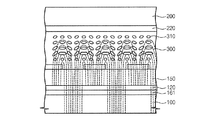
図3は、図2のI-I’線に沿う断面図である。
図3を参照すれば、互いに対向する第1及び第2基板100、200が具備される。第1及び第2基板100、200の間には、液晶層300が介在される。第1基板100上には互いに離隔するように、ゲート電極110gと共通電極161が形成される。ゲート電極110gと共通電極161は、ゲート絶縁膜120によりカバーされる。ゲート絶縁膜120は、共通電極161が形成された領域で第1コンタクトホールC1を有する。
3 is a cross-sectional view taken along the line II ′ of FIG.
Referring to FIG. 3, first and
ゲート絶縁膜120上には、第1データライン141と半導体パターン130が形成される。第1データライン141は、第1コンタクトホールC1を通して共通電極161と電気的に連結される。半導体パターン130は、ゲート電極110gと部分的にオーバーラップする。半導体パターン130は、真性半導体からなるアクティブパターン131と不純物を含むオーミックコンタクトパターン132を含む。オーミックコンタクトパターン132は、二つの部分に分離され、前記分離された部分に沿って、ソース電極140sとドレイン電極140dが形成される。ソース電極140sの端部には、第2データライン142が形成される。
A
ソース電極140s、ドレイン電極140d、第1及び第2データライン141、142は、保護膜150によりカバーされる。保護膜150は、ドレイン電極140dの一部を露出する第2コンタクトホールC2を有する。ゲート絶縁膜120と保護膜150は、透明な無機膜を用いて形成される。例えば、ゲート絶縁膜120と保護膜150は、透明なシリコンナイトライドまたはシリコンオキサイドで形成され得る。ゲート絶縁膜120と保護膜150は、それぞれの上下層に形成された導電性の膜パターンを絶縁させる層間絶縁膜の役割を行なう。保護膜150上には画素電極162が形成される。画素電極162は、第2コンタクトホールC2を満たし、ドレイン電極140dと電気的に連結される。
The
第2基板200上には、遮光膜パターン210とカラーフィルタ220が形成される。遮光膜パターン210は、画素領域PAの境界をカバーし、該当領域で光の透過を遮断する。また、遮光膜パターン210は薄膜トランジスタTをカバーし、外部から薄膜トランジスタTのチャネル領域に光が入射することを遮断する。カラーフィルター220は、画素領域PAに沿って交互に配置される赤色、緑色及び青色カラーフィルタを含む。
A light
図4A及び図4Bは、液晶表示装置の動作過程を説明するための図3の部分拡大図である。
図4Aを参照すれば、液晶表示装置は、液晶層300に印加される電場によってブラック状態とホワイト状態に区分される。前記ブラック状態では、液晶層300に電場が印加されない。前記ブラック状態で、液晶層300に含まれた液晶310の長軸は、第1及び第2基板100、200に対して平行な方向に配列される。液晶310は、長軸と短軸を含む楕円形状を有し、前記長軸の方向によってその配列方向が定義される。上記の配列状態では、液晶層300を通過する光には如何なる位相変化も発生しない。第1及び第2基板100、200の外部には、それぞれ光吸収軸が互いに垂直になるように、偏光板が付着される。前記ブラック状態では、液晶層300を通過する光は、外部に出射できず、液晶表示装置は暗い状態になる。
4A and 4B are partially enlarged views of FIG. 3 for explaining an operation process of the liquid crystal display device.
Referring to FIG. 4A, the liquid crystal display device is classified into a black state and a white state according to an electric field applied to the
図4Bを参照すれば、前記ホワイト状態で、液晶層300に電圧が印加される。このとき、ゲートライン110にゲート信号が印加され、薄膜トランジスタTがターンオンされる。第2データライン142にはデータ信号が印加され、薄膜トランジスタTの作用により映像情報に対応するデータ電圧が画素電極162に印加される。第1データライン141には、一定の共通電圧が伝達され、共通電極161に印加される。共通電極161と画素電極162に印加される電圧の差により、液晶層300に電場が形成される。
Referring to FIG. 4B, a voltage is applied to the
図4Bに示すように、前記電場は上方に凸状をなす放物線形状を有する。液晶310は、誘電率異方性を有し、前記電場によって水平配列状態に対してねじれるように配列される。液晶310は、屈折率異方性を有し、前記ねじれて配列された状態で液晶層300を通過する光は、その位相が変化される。前記位相変化された光は、第2基板200に付加された偏光板を透過して出射し、液晶表示装置は明るい状態になる。
As shown in FIG. 4B, the electric field has a parabolic shape that is convex upward. The
図4Bに示すように、共通電極161において前記電場が形成される領域は、画素電極162にカバーされず切開部170により露出される部分である。これにより、前記ホワイト状態で液晶310のねじれる方向は、切開部170が形成される方向によって変わり得る。図2を再び参照すれば、第1データライン141を基準にして、第1切開部171と第2切開部172は互いに対称になるように傾く。第1切開部171が形成された領域を第1サブ領域とし、第2切開部172が形成された領域を第2サブ領域とすると、前記第1サブ領域と前記第2サブ領域とで液晶310がねじれる方向は、互いに対称になる。したがって、前記第1及び第2サブ領域で光学特性が補償されて、液晶表示装置の視野角が広くなる。
As shown in FIG. 4B, the region where the electric field is formed in the
上記の動作において、第1データライン141は、共通電圧を速かに伝達するために優れた伝導性を有する金属材質で形成される。前記高伝導性金属は、光の透過を遮断し、第1データライン141が形成された領域の面積だけ画素領域PAの開口率が減少する。本実施の形態で、第1データライン141は画素領域PAの短辺と平行な方向に形成される。したがって、第1データライン141は、画素領域PAで最小限の面積を占め、液晶表示装置は最大限の開口率を維持することができる。
In the above operation, the
第1データライン141は、前記第1及び第2サブ領域の境界に位置する。前記境界領域に位置する液晶310は、第1及び第2切開部171、172の両方からの制御を受けて、どちらか一方向に配列されず、その配列が乱れる。すなわち、前記ホワイト状態でも、前記第1及び第2サブ領域の境界では光が外部に出射できず、暗く表示される。したがって、該当領域はいつも暗く表示されるため、前記境界領域に第1データライン141を配置する場合であっても、第1データライン141による追加的な開口率減少は発生しない。
The
上記のように本実施の形態による液晶表示装置は、最大の開口率を維持しながら高画質の映像を表示する。
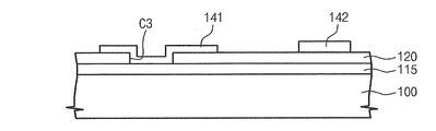
図5は、図1の「A」部分に対する拡大図であり、図6は、図5のII−II’線に沿う断面図である。
図5を参照すれば、表示領域DAの外部の第1データライン141の端部に、行方向に補助ライン115が形成される。補助ライン115は、ゲートライン110と同一材質を用いて同時に形成されることができる。第1データライン141と補助ライン115は、第3コンタクトホールC3を通して電気的に連結される。第2データライン142は補助ライン115と交差する。
As described above, the liquid crystal display device according to the present embodiment displays a high-quality image while maintaining the maximum aperture ratio.
5 is an enlarged view of the “A” portion of FIG. 1, and FIG. 6 is a cross-sectional view taken along the line II-II ′ of FIG.
Referring to FIG. 5,
図6を参照すれば、第1基板100上に補助ライン115が形成される。補助ライン115はゲート絶縁膜120によりカバーされる。ゲート絶縁膜120は第3コンタクトホールC3を有し、これを通して第1データライン141と補助ライン115が電気的に連結される。第2データライン142は、ゲート絶縁膜120により補助ライン115と電気的に絶縁される。
Referring to FIG. 6, the
図7A〜図7Hは、図3の液晶表示装置を製造する過程を説明する断面図である。
図7Aを参照すれば、第1基板100上に透明導電膜が形成される。第1基板100としては、透明で絶縁性を有するガラスやプラスチックが使用される。前記透明導電膜は、酸化亜鉛インジウムや酸化錫インジウムを利用するスパッタリング方法により、第1基板100の全面に蒸着される。前記透明導電膜上にフォトレジスト膜が塗布される。前記フォトレジスト膜が露光及び現像されて、フォトレジストパターンが形成される。前記フォトレジストパターンをエッチングマスクとして、前記透明導電膜がエッチングされる。以下で説明する工程でも、特定の膜をエッチングする場合、フォトレジストパターンを利用する上記のような方法が適用される。前記透明導電膜がエッチングされて、共通電極161が形成される。
7A to 7H are cross-sectional views illustrating a process of manufacturing the liquid crystal display device of FIG.
Referring to FIG. 7A, a transparent conductive film is formed on the
第1基板100の全面にゲート導電膜が形成される。前記ゲート導電膜は、クロム、アルミニウム、アルミニウム合金、モリブデン、またはこれらの化合物など、伝導性の優れた金属材質を用いて単一膜や多層膜として形成される。前記ゲート導電膜がエッチングされて、ゲート電極110gが形成される。図示していないが、前記エッチングの時、ゲート電極110gと共にゲートライン110が形成される。工程手順において、ゲート電極110gは共通電極161より先に形成されることもできる。
A gate conductive film is formed on the entire surface of the
図7Bを参照すれば、第1基板100の全面に、ゲート絶縁膜120と半導体膜が形成される。ゲート絶縁膜120と前記半導体膜は、プラズマ化学気相蒸着法を利用して第1基板100の全面に蒸着される。
ゲート絶縁膜120は、シリコンナイトライドやシリコンオキサイドのような無機膜で形成される。前記半導体膜は、非晶質シリコン材質のアクティブ膜とその上部の不純物を含むオーミックコンタクト膜の二層膜で構成される。前記半導体膜がエッチングされ、予備半導体パターン130’が形成される。予備半導体パターン130’は、ゲート電極110g上の所定領域のみに形成され、予備アクティブパターン131’と予備オーミックコンタクトパターン132’からなる。
Referring to FIG. 7B, a
The
図7Cを参照すれば、ゲート絶縁膜120がエッチングされ、共通電極161を露出する第1コンタクトホールC1が形成される。第1基板100の全面にデータ導電膜140’が形成される。データ導電膜140’は、第1コンタクトホールC1を満たすように形成される。データ導電膜140’は、前記ゲート導電膜と同一な方法で形成されることができる。
Referring to FIG. 7C, the
図7Dを参照すれば、データ導電膜140’がエッチングされる。前記エッチングにより、ソース電極140s、ドレイン電極140d、第1及び第2データライン141、142が形成される。第1データライン141は、第1コンタクトホールC1を通して共通電極161と電気的に連結される。ソース電極140s及びドレイン電極140dに沿って予備半導体パターン130’がエッチングされて、半導体パターン130が形成される。前記エッチングの時、予備オーミックコンタクトパターン132’が二つの部分に分離される。半導体パターン130は、アクティブパターン131とオーミックコンタクトパターン132を含む。
Referring to FIG. 7D, the data conductive layer 140 'is etched. The etching forms the
図7Eを参照すれば、第1基板100の全面に保護膜150が形成される。保護膜150は、ゲート絶縁膜120と同一な材質で、同一な方法により形成されることができる。保護膜150がエッチングされて、ドレイン電極140dを露出する第2コンタクトホールC2が形成される。第1基板100の全面に透明導電膜160’が形成される。透明導電膜160’は、第2コンタクトホールC2に満たす。透明導電膜160’は、共通電極161を形成する時と同一な材質で、同一な方法により形成されることができる。
Referring to FIG. 7E, a
図7Fを参照すれば、透明導電膜160’がエッチングされて、画素電極162が形成される。画素電極162は、第2コンタクトホールC2を通してドレイン電極140dに電気的に連結される。画素電極162は、その内部の所定領域が開口されて切開部170を有する。
図7Gを参照すれば、第2基板200上に遮光膜パターン210が形成される。遮光膜パターン210は、第2基板200上に遮光膜を塗布した後、これをパターニングして形成される。前記遮光膜は、フォトレジスト成分を有し、前記パターニングは別途のエッチング工程なしに露光及び現像により行なわれる。遮光膜パターン210上にカラーフィルタ220が形成される。カラーフィルター220は、カラー層を塗布した後、これをパターニングして形成される。前記カラー層は、カラーを表すフォトレジスト成分を有し、前記パターニングは別途のエッチング工程なしに露光及び現像により行なわれる。前記カラー層の塗布及びパターニング過程は、赤色、緑色及び青色カラーフィルタに対して総3回実施される。
Referring to FIG. 7F, the transparent
Referring to FIG. 7G, a light
図7Hを参照すれば、第1及び第2基板100、200の間に液晶層300が形成され、第1及び第2基板100、200は互いに結合される。液晶層300は、注入方法または滴下方法により形成されることができる。前記注入方法によれば、硬化樹脂を用いて第1及び第2基板100、200を結合するが、所定部分を開口させ、前記開口した部分を通して液晶310を注入して、液晶層300を形成する。前記滴下方法によれば、前記硬化樹脂がエッジ部分に塗布された第1基板100上に液晶310を滴下した後、前記硬化樹脂を硬化しながら、第1及び第2基板100、200を結合する。
Referring to FIG. 7H, a
図8は、本発明の他の実施の形態による、図1の単一画素領域に対する拡大図である。本実施の形態において、上述した実施の形態と重複する構成要素に対して同一な参照符号を使用し、前記重複する構成要素に対する詳細な説明は省略する。
図8を参照すれば、画素領域PAには、薄膜トランジスタT、共通電極161及び画素電極162が具備される。薄膜トランジスタTは、ゲート電極110g、ソース電極140s及びドレイン電極140dを含む。共通電極161と画素電極162は上下にオーバーラップしており、画素領域PAの大部分を占める。
FIG. 8 is an enlarged view of the single pixel region of FIG. 1 according to another embodiment of the present invention. In the present embodiment, the same reference numerals are used for the same components as those in the above-described embodiment, and the detailed description of the overlapping components is omitted.
Referring to FIG. 8, the pixel area PA includes a thin film transistor T, a
共通電極161と第1データライン141は、互いに直接連結される。画素電極162と第2データライン142は、第2コンタクトホールC2を通して互いに電気的に連結される。画素電極162は、所定領域が切開された複数の切開部170を有する。切開部170は、第1切開部171と第2切開部172を含む。第1データライン141は画素領域PAを二等分して、第1及び第2切開部171、172は、第1データライン141に対して対称になるように、斜めに形成される。
The
図9は、図8のIII−III’線に沿う断面図である。
図9を参照すれば、第1基板100上にはゲート電極110gが形成される。ゲート電極110gは、ゲート絶縁膜120によりカバーされる。ゲート絶縁膜120上には、半導体パターン130、共通電極161、第1及び第2データライン141、142が形成される。半導体パターン130は、ゲート電極110gと部分的にオーバーラップし、アクティブパターン131とオーミックコンタクトパターン132を含む。第1及び第2データライン141、142は互いに離隔し、第1データライン141は共通電極161上部に接触して形成される。半導体パターン130上には、ソース電極140sとドレイン電極140dが形成される。
9 is a cross-sectional view taken along the line III-III ′ of FIG.
Referring to FIG. 9, a
共通電極161、ソース電極140s、ドレイン電極140d、第1及び第2データライン141、142は、保護膜150によりカバーされる。保護膜150は、ドレイン電極140dの一部を露出する第2コンタクトホールC2を有する。保護膜150上には画素電極162が形成される。画素電極162は第2コンタクトホールC2を満たして、ドレイン電極140dと電気的に連結される。第2基板200上には、遮光膜パターン210とカラーフィルタ220が形成される。
The
このような構造を有する液晶表示装置の動作過程は、上記の実施の形態の液晶表示装置と殆ど同一である。ただ、共通電極161に共通電圧を印加するにおいて、多少異なる。すなわち、上記の実施の形態では、第1データライン141と共通電極161とがゲート絶縁膜120を介して第1コンタクトホールC1を通して電気的に連結されるが、本実施の形態では、第1データライン141が共通電極161の上部に直接連結される。
The operation process of the liquid crystal display device having such a structure is almost the same as that of the liquid crystal display device of the above embodiment. However, in applying a common voltage to the
第1データライン141は、前記共通電圧を速かに伝達するように、優れた伝導性を有する金属材質で形成される。前記高伝導性金属は、光の透過を遮断し、第1データライン141が形成された領域の面積だけ画素領域PAの開口率が減少する。本実施の形態で、第1データライン141は画素領域PAの短辺と平行に形成される。したがって、第1データライン141は画素領域PAで最小限の面積のみを占め、液晶表示装置は最大の開口率を維持する。特に、第1データライン141は、前記第1及び第2サブ領域の境界に位置するが、前記境界領域は、液晶310の配列が乱れて暗く表示されるため、該当領域に第1データライン141を配置する場合、第1データライン141による追加的な開口率減少は発生しない。したがって、本実施の形態による液晶表示装置は、最大の開口率を維持して、高画質の映像を表示することができる。
The
図10A〜図10Hは、図9の液晶表示装置を製造する過程を説明する断面図である。
図10Aを参照すれば、第1基板100の全面にゲート導電膜が形成される。前記ゲート導電膜がエッチングされて、ゲート電極110gが形成される。図示されていないが、前記エッチングの時、ゲート電極110gと共にゲートライン110が形成される。
図10Bを参照すれば、第1基板100の全面にゲート絶縁膜120が形成される。ゲート絶縁膜120上に半導体膜が形成され、前記半導体膜がエッチングされて予備半導体パターン130’が形成される。予備半導体パターン130’は、予備アクティブパターン131’とその上部の予備オーミックコンタクトパターン132’を含む。
10A to 10H are cross-sectional views illustrating a process of manufacturing the liquid crystal display device of FIG.
Referring to FIG. 10A, a gate conductive layer is formed on the entire surface of the
Referring to FIG. 10B, a
図10Cを参照すれば、ゲート絶縁膜120上に透明導電膜が蒸着される。前記透明導電膜がエッチングされて、共通電極161が形成される。予備半導体パターン130’及び共通電極161上に、第1基板100の全面を覆うようにデータ導電膜140’が蒸着される。
図10Dを参照すれば、データ導電膜140’がエッチングされる。前記エッチングにより、ソース電極140s、ドレイン電極140d、第1及び第2データライン141、142が形成される。第1データライン141は、共通電極161上部に接触する。ソース電極140s及びドレイン電極140dに沿って予備半導体パターン130’がエッチングされて、半導体パターン130が形成される。半導体パターン130は、アクティブパターン131とオーミックコンタクトパターン132を含む。
Referring to FIG. 10C, a transparent conductive film is deposited on the
Referring to FIG. 10D, the data
図10Eを参照すれば、第1基板100の全面に保護膜150が形成される。保護膜150がエッチングされて、ドレイン電極140dを露出する第2コンタクトホールC2が形成される。第1基板100の全面に透明導電膜160’が蒸着される。
図10Fを参照すれば、透明導電膜160’がエッチングされて画素電極162が形成される。透明導電膜160’は第2コンタクトホールC2満たし、画素電極162は、第2コンタクトホールC2を通してドレイン電極140dに電気的に連結される。画素電極162は、その内部の所定領域が開口されて、切開部170を有する。
Referring to FIG. 10E, a
Referring to FIG. 10F, the transparent
図10Gを参照すれば、第2基板200上に遮光膜が形成され、前記遮光膜がパターニングされて遮光膜パターン210が形成される。前記パターニングは、別途のエッチング工程なしに露光及び現像により行なわれることができる。遮光膜パターン210上にカラー層が塗布され、前記カラー層がパターニングされて、カラーフィルタ220が形成される。前記パターニングは、別途のエッチング工程なしに露光及び現像により行なわれることができる。
Referring to FIG. 10G, a light shielding film is formed on the
図10Hを参照すれば、第1及び第2基板100、200の間に液晶層300が形成され、第1及び第2基板100、200は互いに結合される。液晶層300は、注入方法または滴下方法により形成できる。
上記実施形態では、画素領域を2つのサブ領域に分割し、そのサブ領域の間に第1データラインを配置している。しかし、画素領域をさらに3つのサブ領域に分割し、サブ領域間に第1データラインを配置しても良い。ただし、第1データラインの本数の増加による開口率への影響、複数のサブ領域への分割による視野角の改善度合い、などを考慮してサブ領域への分割数を決定するのが良い。
Referring to FIG. 10H, a
In the above embodiment, the pixel area is divided into two sub areas, and the first data line is arranged between the sub areas. However, the pixel area may be further divided into three sub areas, and the first data line may be arranged between the sub areas. However, it is preferable to determine the number of divisions into sub-regions in consideration of the influence on the aperture ratio due to the increase in the number of first data lines, the degree of viewing angle improvement due to division into a plurality of sub-regions, and the like.
上述した本発明の好ましい実施の形態は、例示の目的のために開示されたものであり、本発明の属する技術の分野における通常の知識を有する者であれば、本発明の技術的思想を逸脱しない範囲内で、様々な置換、変形、及び変更が可能であり、このような置換、変更などは、特許請求の範囲に属するものである。 The above-described preferred embodiments of the present invention have been disclosed for the purpose of illustration, and those having ordinary knowledge in the technical field to which the present invention pertains depart from the technical idea of the present invention. Various substitutions, modifications, and alterations are possible within the scope of not being included, and such substitutions, alterations, and the like belong to the scope of the claims.
100第1基板
110ゲートライン
115補助ライン
141第1データライン
142第2データライン
161共通電極
162画素電極
200第2基板
300液晶層
100
Claims (11)
前記第1基板の上部に形成されたゲートラインと、
前記ゲートラインを覆う第1層間絶縁膜と、
前記第1層間絶縁膜上部に形成され、前記画素領域を横切る第1データラインと、
前記第1基板の上部に、前記ゲートラインから離隔して形成され、前記第1データラインの端部と電気的に連結されて、前記第1データラインに電圧を印加する補助ラインと、
前記第1層間絶縁膜上部に形成され、前記ゲートラインと共に前記画素領域を定義する第2データラインと、
前記第1データラインを介して電圧が印加される共通電極と、
前記第1及び第2データラインを覆う第2層間絶縁膜と、
前記第2層間絶縁膜の上部に形成され、前記第2データラインを介して電圧が印加される画素電極と、
前記第1基板と対向する第2基板と、
を含み、
前記画素領域は、前記データラインに沿う第1方向の長さが、前記ゲートラインに沿う第2方向の長さよりも短く、
前記第1データラインは、前記画素領域を前記第1方向に横切るように配置されている、ことを特徴とする表示装置。 A first substrate having a pixel area defined;
A gate line formed on the first substrate;
A first interlayer insulating film covering the gate line;
A first data line formed on the first interlayer insulating film and crossing the pixel region;
An auxiliary line formed on the first substrate and spaced apart from the gate line and electrically connected to an end of the first data line to apply a voltage to the first data line;
A second data line formed on the first interlayer insulating layer and defining the pixel region together with the gate line;
A common electrode to which a voltage is applied through the first data line;
A second interlayer insulating film covering the first and second data lines;
A pixel electrode formed on the second interlayer insulating layer and applied with a voltage through the second data line;
A second substrate facing the first substrate;
Only including,
The pixel region has a length in a first direction along the data line shorter than a length in a second direction along the gate line,
The display device, wherein the first data line is arranged so as to cross the pixel region in the first direction .
前記ゲート電極と平面上で部分的にオーバーラップし、前記第2データラインから分岐するソース電極と、
前記ゲート電極を介して前記ソース電極から離隔し、前記画素電極に電気的に連結されるドレイン電極と、
をさらに含むことを特徴とする請求項1に記載の表示装置。 A gate electrode formed on the first substrate and branched from the gate line;
A source electrode partially overlapping with the gate electrode on a plane and branching from the second data line;
A drain electrode spaced apart from the source electrode through the gate electrode and electrically connected to the pixel electrode;
The display device according to claim 1, further comprising:
前記第1データラインの前記第1部分は前記コンタクトホールに重畳しており、前記第1データラインの前記第2部分は前記コンタクトホールに重畳していない、請求項10に記載の表示装置。 The display device according to claim 10, wherein the first portion of the first data line overlaps the contact hole, and the second portion of the first data line does not overlap the contact hole.
Applications Claiming Priority (2)
| Application Number | Priority Date | Filing Date | Title |
|---|---|---|---|
| KR1020070039419A KR101391884B1 (en) | 2007-04-23 | 2007-04-23 | Display apparatus and method of fabricating the same |
| KR10-2007-0039419 | 2007-04-23 |
Publications (3)
| Publication Number | Publication Date |
|---|---|
| JP2008268961A JP2008268961A (en) | 2008-11-06 |
| JP2008268961A5 JP2008268961A5 (en) | 2011-05-12 |
| JP5323388B2 true JP5323388B2 (en) | 2013-10-23 |
Family
ID=39871824
Family Applications (1)
| Application Number | Title | Priority Date | Filing Date |
|---|---|---|---|
| JP2008112291A Active JP5323388B2 (en) | 2007-04-23 | 2008-04-23 | Display device |
Country Status (3)
| Country | Link |
|---|---|
| US (1) | US8958041B2 (en) |
| JP (1) | JP5323388B2 (en) |
| KR (1) | KR101391884B1 (en) |
Families Citing this family (11)
| Publication number | Priority date | Publication date | Assignee | Title |
|---|---|---|---|---|
| CN102282504B (en) * | 2009-05-29 | 2014-12-03 | 夏普株式会社 | Liquid crystal display device |
| US20130155364A1 (en) * | 2011-12-14 | 2013-06-20 | Shenzhen China Star Optoelectronics Technology Co.,Ltd. | Method of reducing parasitic capacitance of liquid crystal display device and liquid crystal display device |
| KR101929345B1 (en) * | 2011-12-21 | 2018-12-17 | 엘지디스플레이 주식회사 | Fringe field switching liquid crystal display device |
| JP6116220B2 (en) * | 2012-12-12 | 2017-04-19 | 三菱電機株式会社 | LCD panel |
| KR102105285B1 (en) | 2013-09-03 | 2020-06-01 | 삼성디스플레이 주식회사 | Liquid crystal display |
| KR102046848B1 (en) * | 2013-12-20 | 2019-11-20 | 엘지디스플레이 주식회사 | Liquid Display Device |
| CN104460136B (en) * | 2014-12-30 | 2017-06-23 | 京东方科技集团股份有限公司 | Liquid crystal grating and preparation method thereof and driving method, mosaic screen |
| CN105182590B (en) * | 2015-10-10 | 2018-10-19 | 京东方科技集团股份有限公司 | Touch display panel and preparation method thereof and display device |
| KR102148491B1 (en) * | 2015-12-14 | 2020-08-26 | 엘지디스플레이 주식회사 | Thin film transistor substrate |
| KR102459575B1 (en) * | 2016-01-06 | 2022-10-27 | 삼성디스플레이 주식회사 | Display device |
| US10503032B2 (en) | 2018-03-30 | 2019-12-10 | Panasonic Liquid Crystal Display Co., Ltd. | Liquid crystal display device |
Family Cites Families (12)
| Publication number | Priority date | Publication date | Assignee | Title |
|---|---|---|---|---|
| JPH09120081A (en) | 1995-10-25 | 1997-05-06 | Toshiba Corp | Liquid crystal display device and production of liquid crystal display device |
| KR100268104B1 (en) * | 1997-08-13 | 2000-10-16 | 윤종용 | Ips mode lcd with common electrode lines and methods of manufacturing the same |
| JP3349935B2 (en) | 1997-12-05 | 2002-11-25 | アルプス電気株式会社 | Active matrix type liquid crystal display |
| KR100507271B1 (en) | 1999-06-30 | 2005-08-10 | 비오이 하이디스 테크놀로지 주식회사 | LCD having high aperture ratio and high transmittance and method for manufacturing the same |
| JP4724339B2 (en) | 1999-09-07 | 2011-07-13 | 株式会社日立製作所 | Liquid crystal display |
| TW513604B (en) | 2001-02-14 | 2002-12-11 | Au Optronics Corp | A thin film transistor liquid crystal display |
| KR100494702B1 (en) | 2001-12-26 | 2005-06-13 | 비오이 하이디스 테크놀로지 주식회사 | Fringe field switching liquid crystal display |
| JP3881248B2 (en) * | 2002-01-17 | 2007-02-14 | 株式会社日立製作所 | Liquid crystal display device and image display device |
| KR100913739B1 (en) | 2002-12-20 | 2009-08-24 | 엘지디스플레이 주식회사 | An array substrate for In-Plane switching mode LCD and the method for fabricating the same |
| KR100920923B1 (en) | 2002-12-31 | 2009-10-12 | 엘지디스플레이 주식회사 | An array substrate for In-Plane switching mode LCD and the method for fabricating the same |
| KR101071711B1 (en) * | 2003-12-29 | 2011-10-12 | 엘지디스플레이 주식회사 | In-Plane Switching mode Liquid crystal display device |
| KR101220205B1 (en) * | 2005-12-29 | 2013-01-09 | 엘지디스플레이 주식회사 | Liquid crystal display device |
-
2007
- 2007-04-23 KR KR1020070039419A patent/KR101391884B1/en active IP Right Grant
-
2008
- 2008-02-12 US US12/030,080 patent/US8958041B2/en active Active
- 2008-04-23 JP JP2008112291A patent/JP5323388B2/en active Active
Also Published As
| Publication number | Publication date |
|---|---|
| KR20080095076A (en) | 2008-10-28 |
| JP2008268961A (en) | 2008-11-06 |
| US8958041B2 (en) | 2015-02-17 |
| US20080259261A1 (en) | 2008-10-23 |
| KR101391884B1 (en) | 2014-05-07 |
Similar Documents
| Publication | Publication Date | Title |
|---|---|---|
| JP5323388B2 (en) | Display device | |
| US7742117B2 (en) | Liquid crystal display panel | |
| KR102054233B1 (en) | Liquid crystal display device and method for fabricating the same | |
| KR100510566B1 (en) | In-plane switching mode liquid crystal display device | |
| US8345175B2 (en) | Array substrate for liquid crystal display device and method of manufacturing the same | |
| JP5460123B2 (en) | Liquid crystal display | |
| JP2004341530A (en) | Vertical alignment type liquid crystal display device | |
| KR102416573B1 (en) | Display device and manufacturing method thereof | |
| US12082441B2 (en) | Display apparatus having a narrow viewing angle | |
| KR20110122783A (en) | Array substrate for liquid crystal display device and method of fabricating the same | |
| KR101955992B1 (en) | Array substrate for fringe field switching mode liquid crystal display device and method for fabricating the same | |
| KR20070082090A (en) | Display substrate and method for manufacturing the same | |
| KR20110105612A (en) | In-plane switching mode liquid crystal display device and the method of fabricating the same | |
| KR101897747B1 (en) | Array substrate for fringe field switching mode liquid crystal display device and method for fabricating the same | |
| KR20110132724A (en) | In-plane switching mode liquid crystal display device and the method of fabricating the same | |
| KR100919634B1 (en) | Method for fabricating a Transflective liquid crystal display device and the same | |
| KR100470022B1 (en) | LCD and method for fabricating the same | |
| KR20070063967A (en) | An array substrate for in-plane switching mode lcd and method of fabricating of the same | |
| KR101189144B1 (en) | An array substrate for In-Plane switching mode LCD and method of fabricating of the same | |
| KR101215943B1 (en) | The array substrate for liquid crystal display device and method of fabricating the same | |
| KR20080051366A (en) | In-plane switching mode liquid crystal display device and the method for fabricating thereof | |
| KR20080100903A (en) | Display apparatus and method of manufactruing the same | |
| KR20090022078A (en) | Array substrate for in-plane switching mode liquid crystal display device and the method for fabricating the same | |
| KR20050062692A (en) | Liquid crystal display device and method for manufacturing the same | |
| KR100620845B1 (en) | Method of Multidomain Liquid Crystal Display |
Legal Events
| Date | Code | Title | Description |
|---|---|---|---|
| A521 | Request for written amendment filed |
Free format text: JAPANESE INTERMEDIATE CODE: A523 Effective date: 20110329 |
|
| A621 | Written request for application examination |
Free format text: JAPANESE INTERMEDIATE CODE: A621 Effective date: 20110329 |
|
| RD02 | Notification of acceptance of power of attorney |
Free format text: JAPANESE INTERMEDIATE CODE: A7422 Effective date: 20110329 |
|
| A521 | Request for written amendment filed |
Free format text: JAPANESE INTERMEDIATE CODE: A523 Effective date: 20120228 |
|
| A977 | Report on retrieval |
Free format text: JAPANESE INTERMEDIATE CODE: A971007 Effective date: 20121212 |
|
| A711 | Notification of change in applicant |
Free format text: JAPANESE INTERMEDIATE CODE: A712 Effective date: 20121213 |
|
| A521 | Request for written amendment filed |
Free format text: JAPANESE INTERMEDIATE CODE: A523 Effective date: 20130322 |
|
| A131 | Notification of reasons for refusal |
Free format text: JAPANESE INTERMEDIATE CODE: A131 Effective date: 20130409 |
|
| A521 | Request for written amendment filed |
Free format text: JAPANESE INTERMEDIATE CODE: A523 Effective date: 20130520 |
|
| TRDD | Decision of grant or rejection written | ||
| A01 | Written decision to grant a patent or to grant a registration (utility model) |
Free format text: JAPANESE INTERMEDIATE CODE: A01 Effective date: 20130702 |
|
| A61 | First payment of annual fees (during grant procedure) |
Free format text: JAPANESE INTERMEDIATE CODE: A61 Effective date: 20130717 |
|
| R150 | Certificate of patent or registration of utility model |
Ref document number: 5323388 Country of ref document: JP Free format text: JAPANESE INTERMEDIATE CODE: R150 Free format text: JAPANESE INTERMEDIATE CODE: R150 |
|
| R250 | Receipt of annual fees |
Free format text: JAPANESE INTERMEDIATE CODE: R250 |
|
| R250 | Receipt of annual fees |
Free format text: JAPANESE INTERMEDIATE CODE: R250 |
|
| R250 | Receipt of annual fees |
Free format text: JAPANESE INTERMEDIATE CODE: R250 |
|
| R250 | Receipt of annual fees |
Free format text: JAPANESE INTERMEDIATE CODE: R250 |
|
| R250 | Receipt of annual fees |
Free format text: JAPANESE INTERMEDIATE CODE: R250 |
|
| R250 | Receipt of annual fees |
Free format text: JAPANESE INTERMEDIATE CODE: R250 |
|
| R250 | Receipt of annual fees |
Free format text: JAPANESE INTERMEDIATE CODE: R250 |
|
| R250 | Receipt of annual fees |
Free format text: JAPANESE INTERMEDIATE CODE: R250 |