JP5321069B2 - 触媒化学気相成長装置の触媒体支持構造 - Google Patents
触媒化学気相成長装置の触媒体支持構造 Download PDFInfo
- Publication number
- JP5321069B2 JP5321069B2 JP2009001520A JP2009001520A JP5321069B2 JP 5321069 B2 JP5321069 B2 JP 5321069B2 JP 2009001520 A JP2009001520 A JP 2009001520A JP 2009001520 A JP2009001520 A JP 2009001520A JP 5321069 B2 JP5321069 B2 JP 5321069B2
- Authority
- JP
- Japan
- Prior art keywords
- catalyst body
- catalyst
- frame
- chemical vapor
- vapor deposition
- Prior art date
- Legal status (The legal status is an assumption and is not a legal conclusion. Google has not performed a legal analysis and makes no representation as to the accuracy of the status listed.)
- Expired - Fee Related
Links
- 239000003054 catalyst Substances 0.000 title claims description 198
- 238000004050 hot filament vapor deposition Methods 0.000 title claims description 26
- 238000000151 deposition Methods 0.000 claims description 47
- 230000008021 deposition Effects 0.000 claims description 47
- 229910052751 metal Inorganic materials 0.000 claims description 31
- 239000002184 metal Substances 0.000 claims description 31
- 230000006835 compression Effects 0.000 claims description 17
- 238000007906 compression Methods 0.000 claims description 17
- 239000000470 constituent Substances 0.000 claims description 6
- 230000003197 catalytic effect Effects 0.000 claims 1
- 239000010408 film Substances 0.000 description 44
- 239000007789 gas Substances 0.000 description 40
- 238000000034 method Methods 0.000 description 24
- 230000002265 prevention Effects 0.000 description 13
- 238000004140 cleaning Methods 0.000 description 12
- 239000000758 substrate Substances 0.000 description 11
- 239000002994 raw material Substances 0.000 description 10
- 239000010409 thin film Substances 0.000 description 8
- 238000004804 winding Methods 0.000 description 8
- 230000015572 biosynthetic process Effects 0.000 description 6
- 238000001816 cooling Methods 0.000 description 6
- 238000003780 insertion Methods 0.000 description 5
- 230000037431 insertion Effects 0.000 description 5
- 239000000463 material Substances 0.000 description 5
- 229910001220 stainless steel Inorganic materials 0.000 description 5
- 239000010935 stainless steel Substances 0.000 description 5
- WFKWXMTUELFFGS-UHFFFAOYSA-N tungsten Chemical compound [W] WFKWXMTUELFFGS-UHFFFAOYSA-N 0.000 description 5
- ZOKXTWBITQBERF-UHFFFAOYSA-N Molybdenum Chemical compound [Mo] ZOKXTWBITQBERF-UHFFFAOYSA-N 0.000 description 4
- 239000000919 ceramic Substances 0.000 description 4
- 238000006243 chemical reaction Methods 0.000 description 4
- 229910052750 molybdenum Inorganic materials 0.000 description 4
- 239000011733 molybdenum Substances 0.000 description 4
- 238000000354 decomposition reaction Methods 0.000 description 3
- 238000010438 heat treatment Methods 0.000 description 3
- 238000002844 melting Methods 0.000 description 3
- 230000008018 melting Effects 0.000 description 3
- 239000007769 metal material Substances 0.000 description 3
- 230000001681 protective effect Effects 0.000 description 3
- IJGRMHOSHXDMSA-UHFFFAOYSA-N Atomic nitrogen Chemical compound N#N IJGRMHOSHXDMSA-UHFFFAOYSA-N 0.000 description 2
- MCMNRKCIXSYSNV-UHFFFAOYSA-N Zirconium dioxide Chemical compound O=[Zr]=O MCMNRKCIXSYSNV-UHFFFAOYSA-N 0.000 description 2
- PNEYBMLMFCGWSK-UHFFFAOYSA-N aluminium oxide Inorganic materials [O-2].[O-2].[O-2].[Al+3].[Al+3] PNEYBMLMFCGWSK-UHFFFAOYSA-N 0.000 description 2
- 230000036760 body temperature Effects 0.000 description 2
- 238000010586 diagram Methods 0.000 description 2
- 238000000605 extraction Methods 0.000 description 2
- 238000004519 manufacturing process Methods 0.000 description 2
- 238000003825 pressing Methods 0.000 description 2
- 239000004065 semiconductor Substances 0.000 description 2
- BLRPTPMANUNPDV-UHFFFAOYSA-N Silane Chemical compound [SiH4] BLRPTPMANUNPDV-UHFFFAOYSA-N 0.000 description 1
- 239000002253 acid Substances 0.000 description 1
- 238000005452 bending Methods 0.000 description 1
- 238000005422 blasting Methods 0.000 description 1
- 238000007664 blowing Methods 0.000 description 1
- 238000004523 catalytic cracking Methods 0.000 description 1
- 238000003421 catalytic decomposition reaction Methods 0.000 description 1
- 230000003749 cleanliness Effects 0.000 description 1
- 238000003795 desorption Methods 0.000 description 1
- 238000001035 drying Methods 0.000 description 1
- 239000000428 dust Substances 0.000 description 1
- 230000005611 electricity Effects 0.000 description 1
- 239000011888 foil Substances 0.000 description 1
- 230000020169 heat generation Effects 0.000 description 1
- 238000009434 installation Methods 0.000 description 1
- 239000000203 mixture Substances 0.000 description 1
- 229910052757 nitrogen Inorganic materials 0.000 description 1
- 230000002093 peripheral effect Effects 0.000 description 1
- 239000004033 plastic Substances 0.000 description 1
- 229920000642 polymer Polymers 0.000 description 1
- 229910000077 silane Inorganic materials 0.000 description 1
- 150000003377 silicon compounds Chemical class 0.000 description 1
- 239000000126 substance Substances 0.000 description 1
- XLYOFNOQVPJJNP-UHFFFAOYSA-N water Substances O XLYOFNOQVPJJNP-UHFFFAOYSA-N 0.000 description 1
- 230000037303 wrinkles Effects 0.000 description 1
Images

Landscapes
- Chemical Vapour Deposition (AREA)
- Drying Of Semiconductors (AREA)
Description
最初に、本発明の触媒体支持構造が適用される触媒化学気相成長装置の概要について説明する。図10は、連続式の触媒化学気相成長装置を示す断面図である。触媒化学気相成長装置100は、筐体(真空容器)103と、筐体103の下方から原料ガスを供給する原料ガス供給手段102と、電力線111を介して電力供給手段101に接続して通電加熱する触媒体4と、触媒体4を張架する把持部材と、把持部材を防着する防着ユニット1と、成膜する基材フィルム107を成膜エリアに引き出して、成膜した基材フィルム117を巻き取るローラ機構105と、筐体103の下方に接続され使用済みの原料ガスを排気する排気手段(真空ポンプ)104を備える。矢印aは、原料ガスの流れを示す。原料ガス供給手段102から供給された原料ガスは、多数のガス吹き出し孔122を有するガス供給器112から真空容器103内に放出される。ローラ機構105は、3つのローラ105A,105B,105Cと複数のテンションローラ115(図5では2つのテンションローラ)からなる。巻装ローラ105Aに予め巻装された基材フィルム107は、触媒体4近傍の成膜エリアに引き出されて冷却ローラ105Bに密着され、基材フィルム107の始端部が巻取りローラ105Cに巻き取られる。冷却ローラ105Bには冷却手段が備わり、基材フィルム107を低温に保持することで、分解された高温ガスを基材フィルム107上に成膜させる。そして、成膜済みの基材フィルム117が巻取りローラ105Cに巻き取られる。テンションローラ115は、基材フィルム107(及び117)に所定のテンションをかけることで、基材フィルム107(及び117)に皺が寄らないようにする。基材フィルム107は、フィルム状の基板を使用したり、板状の基板を搬送フィルムに貼り付けて使用する。
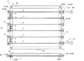
次に、本発明の触媒体支持構造に使用される触媒体支持枠2の構造について説明する。図11(a)は、本実施形態の触媒体支持枠を示す正面図であり、図11(b)は、その側面図である。本実施形態の触媒体支持枠2は、断面四角形状で棒状の橋渡し部材80と断面四角形状で棒状の枠体21(20)をそれぞれ2つずつ対向配置させて、ネジ、ボルト等の固定手段により固定して組み合わせた四角形状の枠である(図11(a))。触媒体4は、断面円形状で軸方向に真っ直ぐな棒形状の単線であり、図11(a)では触媒体4がそれぞれ平行となる位置で、隣り合う触媒体4同士の中心間隔だけずらした位置で向かい合って配された同一形状の1対の導電金具50(51と52)にて触媒体4がそれぞれ2本ずつ把持されている。そして橋渡し部材80に近接した導電金具53に触媒体4がそれぞれ1本ずつ把持されている。本実施形態では合計6本の触媒体4が触媒体支持枠2に張架されている。そして、一方側の枠体21には、触媒体4を張架する方向に張力を与える複数のスプリング6が内蔵されている(図11(a))。
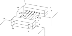
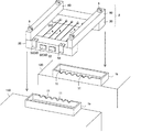
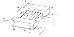
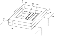
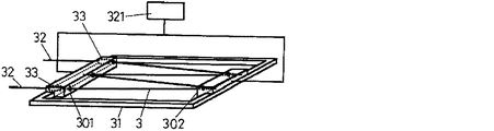
本発明の第1の実施形態の触媒化学気相成長装置の防着ユニット、並びに防着ユニットを備えた触媒体支持構造、及び防着ユニットの取り付け方法について、以下に説明する。図1は、本実施形態の防着ユニットを取り付けた触媒体支持構造を示す斜視図である。図2から図4は、防着ユニットの取り付け過程を示す斜視図である。
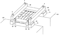
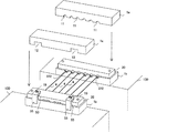
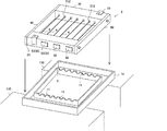
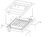
本発明の第2の実施形態の触媒化学気相成長装置の防着ユニット、並びに防着ユニットを備えた触媒体支持構造、及び防着ユニットの取り付け方法について、以下に説明する。図7は、本実施形態の防着ユニットを取り付けた触媒体支持構造を示す斜視図である。図8と図9は、上記防着ユニットの取り付け過程を示す斜視図である。
1a 防着ユニットの上側部材、
1b 防着ユニットの下側部材、
2 触媒体支持枠、
20 枠構成部材(把持部材、枠体)、
4 触媒体、
50、51、52、53 導電金具、
55 電極プレート、
6 圧縮コイルばね(スプリング)、
80 橋渡し部材、
100 触媒化学気相成長装置、
130 支柱(側壁)
Claims (1)
- 所定間隔で配される触媒体を介して向かい合う一対の枠構成部材と、前記触媒体の両側をそれぞれ把持しつつ前記枠構成部材とは電気絶縁された状態で前記触媒体に通電する電気回路を構成する複数の導電金具と、向かい合う導電金具のうち一方の導電金具を他方の導電金具から離す方向に押す圧縮コイルばねと、前記導電金具と電気絶縁された状態で前記枠構成部材を覆う防着ユニットを備え、前記圧縮コイルばねが前記枠構成部材に内蔵されており、前記圧縮コイルばねを通電することなく前記触媒体に通電する構成とされ、前記防着ユニットは、前記触媒体の軸付近を境目として前記触媒体の軸と略垂直方向に上下に分割する上側部材と下側部材からなり、これら上側部材と下側部材とが前記触媒体に非接触の状態で組み合わさっていることを特徴とする触媒化学気相成長装置の触媒体支持構造。
Priority Applications (1)
| Application Number | Priority Date | Filing Date | Title |
|---|---|---|---|
| JP2009001520A JP5321069B2 (ja) | 2009-01-07 | 2009-01-07 | 触媒化学気相成長装置の触媒体支持構造 |
Applications Claiming Priority (1)
| Application Number | Priority Date | Filing Date | Title |
|---|---|---|---|
| JP2009001520A JP5321069B2 (ja) | 2009-01-07 | 2009-01-07 | 触媒化学気相成長装置の触媒体支持構造 |
Publications (2)
| Publication Number | Publication Date |
|---|---|
| JP2010159450A JP2010159450A (ja) | 2010-07-22 |
| JP5321069B2 true JP5321069B2 (ja) | 2013-10-23 |
Family
ID=42576832
Family Applications (1)
| Application Number | Title | Priority Date | Filing Date |
|---|---|---|---|
| JP2009001520A Expired - Fee Related JP5321069B2 (ja) | 2009-01-07 | 2009-01-07 | 触媒化学気相成長装置の触媒体支持構造 |
Country Status (1)
| Country | Link |
|---|---|
| JP (1) | JP5321069B2 (ja) |
Families Citing this family (1)
| Publication number | Priority date | Publication date | Assignee | Title |
|---|---|---|---|---|
| DE102011018324A1 (de) * | 2011-04-20 | 2012-10-25 | Forschungszentrum Jülich GmbH | Heißdrahtverfahren zur Abscheidung von Halbleiter-Material auf einem Substrat und Vorrichtung zur Durchführung des Verfahrens |
Family Cites Families (4)
| Publication number | Priority date | Publication date | Assignee | Title |
|---|---|---|---|---|
| JPH0620963A (ja) * | 1991-12-17 | 1994-01-28 | Matsushita Electric Ind Co Ltd | 真空薄膜堆積装置 |
| JP4435395B2 (ja) * | 2000-09-14 | 2010-03-17 | キヤノンアネルバ株式会社 | 発熱体cvd装置 |
| JP4373723B2 (ja) * | 2003-06-27 | 2009-11-25 | 信越半導体株式会社 | シリンダ型気相成長装置 |
| JP4004510B2 (ja) * | 2005-03-23 | 2007-11-07 | 有限会社マテリアルデザインファクトリ− | 触媒cvd装置 |
-
2009
- 2009-01-07 JP JP2009001520A patent/JP5321069B2/ja not_active Expired - Fee Related
Also Published As
| Publication number | Publication date |
|---|---|
| JP2010159450A (ja) | 2010-07-22 |
Similar Documents
| Publication | Publication Date | Title |
|---|---|---|
| JP3780364B2 (ja) | 発熱体cvd装置 | |
| CN102308675B (zh) | 用于等离子体工艺的接地回流路径 | |
| KR100817644B1 (ko) | 기판 처리 장치 | |
| KR100688838B1 (ko) | 촉매 화학기상증착장치 및 촉매 화학기상증착방법 | |
| JP3787816B2 (ja) | 発熱体cvd装置 | |
| CN101246835A (zh) | 基片支架组件 | |
| JP5321069B2 (ja) | 触媒化学気相成長装置の触媒体支持構造 | |
| JP2000303182A (ja) | 化学蒸着装置 | |
| JP2005129318A (ja) | プラズマディスプレイ装置の解体方法および解体装置 | |
| JP4435395B2 (ja) | 発熱体cvd装置 | |
| KR20060103341A (ko) | 플라즈마 처리 장치 | |
| KR101323360B1 (ko) | 히터 유닛 및 이를 포함하는 기판 처리 장치 | |
| KR101587793B1 (ko) | 히터 보호용 프로세스 키트 및 이를 이용한 챔버 세정방법 | |
| JP3887690B2 (ja) | 発熱体cvd装置における発熱体と電力供給機構との間の接続構造 | |
| JP2010059468A (ja) | 触媒化学気相成長装置の触媒体支持構造 | |
| JP2009038398A (ja) | シリコン膜及びシリコン窒化膜の製造法 | |
| KR20230094042A (ko) | 기판 거치 장치 | |
| TW571336B (en) | Heat treatment equipment | |
| JP2008113014A (ja) | 発熱体cvd装置及び成膜方法 | |
| JP4913947B2 (ja) | 保護ガスシールド装置 | |
| JP2003086512A (ja) | 真空処理装置 | |
| JP2000306844A (ja) | 処理装置 | |
| JP6099508B2 (ja) | ガス捕捉体およびそれを備えた半導体製造装置 | |
| JP2005352018A (ja) | 真空処理装置 | |
| JP5453985B2 (ja) | 支持台 |
Legal Events
| Date | Code | Title | Description |
|---|---|---|---|
| A621 | Written request for application examination |
Free format text: JAPANESE INTERMEDIATE CODE: A621 Effective date: 20111130 |
|
| A977 | Report on retrieval |
Free format text: JAPANESE INTERMEDIATE CODE: A971007 Effective date: 20130426 |
|
| A131 | Notification of reasons for refusal |
Free format text: JAPANESE INTERMEDIATE CODE: A131 Effective date: 20130502 |
|
| A521 | Written amendment |
Free format text: JAPANESE INTERMEDIATE CODE: A523 Effective date: 20130515 |
|
| TRDD | Decision of grant or rejection written | ||
| A01 | Written decision to grant a patent or to grant a registration (utility model) |
Free format text: JAPANESE INTERMEDIATE CODE: A01 Effective date: 20130604 |
|
| A61 | First payment of annual fees (during grant procedure) |
Free format text: JAPANESE INTERMEDIATE CODE: A61 Effective date: 20130701 |
|
| R150 | Certificate of patent or registration of utility model |
Ref document number: 5321069 Country of ref document: JP Free format text: JAPANESE INTERMEDIATE CODE: R150 Free format text: JAPANESE INTERMEDIATE CODE: R150 |
|
| R250 | Receipt of annual fees |
Free format text: JAPANESE INTERMEDIATE CODE: R250 |
|
| R250 | Receipt of annual fees |
Free format text: JAPANESE INTERMEDIATE CODE: R250 |
|
| R250 | Receipt of annual fees |
Free format text: JAPANESE INTERMEDIATE CODE: R250 |
|
| LAPS | Cancellation because of no payment of annual fees |