JP5309359B2 - Film thickness measuring apparatus and film thickness measuring method - Google Patents
Film thickness measuring apparatus and film thickness measuring method Download PDFInfo
- Publication number
- JP5309359B2 JP5309359B2 JP2008162046A JP2008162046A JP5309359B2 JP 5309359 B2 JP5309359 B2 JP 5309359B2 JP 2008162046 A JP2008162046 A JP 2008162046A JP 2008162046 A JP2008162046 A JP 2008162046A JP 5309359 B2 JP5309359 B2 JP 5309359B2
- Authority
- JP
- Japan
- Prior art keywords
- layer
- film thickness
- wavelength
- measured
- wave number
- Prior art date
- Legal status (The legal status is an assumption and is not a legal conclusion. Google has not performed a legal analysis and makes no representation as to the accuracy of the status listed.)
- Active
Links
- 238000000034 method Methods 0.000 title claims abstract description 146
- 238000005259 measurement Methods 0.000 claims abstract description 181
- 238000006243 chemical reaction Methods 0.000 claims description 70
- 239000000758 substrate Substances 0.000 claims description 48
- 238000009826 distribution Methods 0.000 claims description 36
- 238000005457 optimization Methods 0.000 claims description 25
- 230000014509 gene expression Effects 0.000 claims description 20
- 238000002834 transmittance Methods 0.000 claims description 16
- 230000001678 irradiating effect Effects 0.000 claims description 5
- 230000001131 transforming effect Effects 0.000 claims description 2
- 238000000985 reflectance spectrum Methods 0.000 abstract description 63
- 230000003287 optical effect Effects 0.000 abstract description 40
- 238000003384 imaging method Methods 0.000 abstract description 11
- 230000001066 destructive effect Effects 0.000 abstract 1
- 230000035515 penetration Effects 0.000 abstract 1
- 239000010410 layer Substances 0.000 description 248
- 239000010408 film Substances 0.000 description 234
- 230000008569 process Effects 0.000 description 77
- 238000012545 processing Methods 0.000 description 74
- 238000001514 detection method Methods 0.000 description 50
- 238000004364 calculation method Methods 0.000 description 48
- 238000001228 spectrum Methods 0.000 description 44
- 238000010586 diagram Methods 0.000 description 37
- 230000006870 function Effects 0.000 description 36
- 230000008033 biological extinction Effects 0.000 description 32
- 229910004298 SiO 2 Inorganic materials 0.000 description 17
- 238000004458 analytical method Methods 0.000 description 14
- 239000000835 fiber Substances 0.000 description 12
- XUIMIQQOPSSXEZ-UHFFFAOYSA-N Silicon Chemical compound [Si] XUIMIQQOPSSXEZ-UHFFFAOYSA-N 0.000 description 11
- 229910052710 silicon Inorganic materials 0.000 description 11
- 239000010703 silicon Substances 0.000 description 11
- 239000006185 dispersion Substances 0.000 description 10
- 239000010409 thin film Substances 0.000 description 9
- 230000008859 change Effects 0.000 description 8
- 238000012986 modification Methods 0.000 description 8
- 230000004048 modification Effects 0.000 description 8
- 239000000243 solution Substances 0.000 description 8
- 230000000737 periodic effect Effects 0.000 description 7
- 230000007246 mechanism Effects 0.000 description 6
- 238000005498 polishing Methods 0.000 description 6
- 238000002310 reflectometry Methods 0.000 description 6
- 238000013461 design Methods 0.000 description 5
- 238000000691 measurement method Methods 0.000 description 5
- 239000000523 sample Substances 0.000 description 5
- 238000012360 testing method Methods 0.000 description 5
- 239000013307 optical fiber Substances 0.000 description 4
- 238000007517 polishing process Methods 0.000 description 4
- 238000005070 sampling Methods 0.000 description 4
- 230000035945 sensitivity Effects 0.000 description 4
- 239000010421 standard material Substances 0.000 description 4
- 230000001419 dependent effect Effects 0.000 description 3
- 239000011521 glass Substances 0.000 description 3
- 239000002952 polymeric resin Substances 0.000 description 3
- 229920003002 synthetic resin Polymers 0.000 description 3
- 238000000411 transmission spectrum Methods 0.000 description 3
- XLYOFNOQVPJJNP-UHFFFAOYSA-N water Substances O XLYOFNOQVPJJNP-UHFFFAOYSA-N 0.000 description 3
- 238000005033 Fourier transform infrared spectroscopy Methods 0.000 description 2
- 229910000530 Gallium indium arsenide Inorganic materials 0.000 description 2
- 238000010521 absorption reaction Methods 0.000 description 2
- 230000005540 biological transmission Effects 0.000 description 2
- 230000000295 complement effect Effects 0.000 description 2
- 238000012790 confirmation Methods 0.000 description 2
- 230000007423 decrease Effects 0.000 description 2
- 230000000694 effects Effects 0.000 description 2
- 239000012212 insulator Substances 0.000 description 2
- 239000007788 liquid Substances 0.000 description 2
- 229910044991 metal oxide Inorganic materials 0.000 description 2
- 150000004706 metal oxides Chemical class 0.000 description 2
- 239000004065 semiconductor Substances 0.000 description 2
- 125000006850 spacer group Chemical group 0.000 description 2
- 230000003595 spectral effect Effects 0.000 description 2
- 238000005311 autocorrelation function Methods 0.000 description 1
- 230000006399 behavior Effects 0.000 description 1
- 238000005520 cutting process Methods 0.000 description 1
- 230000008030 elimination Effects 0.000 description 1
- 238000003379 elimination reaction Methods 0.000 description 1
- 238000005516 engineering process Methods 0.000 description 1
- 239000000284 extract Substances 0.000 description 1
- 229910052736 halogen Inorganic materials 0.000 description 1
- 150000002367 halogens Chemical class 0.000 description 1
- 238000002347 injection Methods 0.000 description 1
- 239000007924 injection Substances 0.000 description 1
- 239000004973 liquid crystal related substance Substances 0.000 description 1
- 238000004519 manufacturing process Methods 0.000 description 1
- 239000000463 material Substances 0.000 description 1
- 230000003071 parasitic effect Effects 0.000 description 1
- 230000010287 polarization Effects 0.000 description 1
- 238000002360 preparation method Methods 0.000 description 1
- 230000001902 propagating effect Effects 0.000 description 1
- 239000013074 reference sample Substances 0.000 description 1
- 230000004044 response Effects 0.000 description 1
- 229910052594 sapphire Inorganic materials 0.000 description 1
- 239000010980 sapphire Substances 0.000 description 1
- 239000002356 single layer Substances 0.000 description 1
- 239000002904 solvent Substances 0.000 description 1
- 238000003860 storage Methods 0.000 description 1
- 239000000126 substance Substances 0.000 description 1
Images


Classifications
-
- G—PHYSICS
- G01—MEASURING; TESTING
- G01N—INVESTIGATING OR ANALYSING MATERIALS BY DETERMINING THEIR CHEMICAL OR PHYSICAL PROPERTIES
- G01N21/00—Investigating or analysing materials by the use of optical means, i.e. using sub-millimetre waves, infrared, visible or ultraviolet light
- G01N21/17—Systems in which incident light is modified in accordance with the properties of the material investigated
- G01N21/59—Transmissivity
-
- G—PHYSICS
- G01—MEASURING; TESTING
- G01B—MEASURING LENGTH, THICKNESS OR SIMILAR LINEAR DIMENSIONS; MEASURING ANGLES; MEASURING AREAS; MEASURING IRREGULARITIES OF SURFACES OR CONTOURS
- G01B11/00—Measuring arrangements characterised by the use of optical techniques
- G01B11/02—Measuring arrangements characterised by the use of optical techniques for measuring length, width or thickness
- G01B11/06—Measuring arrangements characterised by the use of optical techniques for measuring length, width or thickness for measuring thickness ; e.g. of sheet material
- G01B11/0616—Measuring arrangements characterised by the use of optical techniques for measuring length, width or thickness for measuring thickness ; e.g. of sheet material of coating
- G01B11/0625—Measuring arrangements characterised by the use of optical techniques for measuring length, width or thickness for measuring thickness ; e.g. of sheet material of coating with measurement of absorption or reflection
-
- G—PHYSICS
- G01—MEASURING; TESTING
- G01N—INVESTIGATING OR ANALYSING MATERIALS BY DETERMINING THEIR CHEMICAL OR PHYSICAL PROPERTIES
- G01N21/00—Investigating or analysing materials by the use of optical means, i.e. using sub-millimetre waves, infrared, visible or ultraviolet light
- G01N21/17—Systems in which incident light is modified in accordance with the properties of the material investigated
- G01N21/55—Specular reflectivity
Landscapes
- Physics & Mathematics (AREA)
- General Physics & Mathematics (AREA)
- Health & Medical Sciences (AREA)
- Life Sciences & Earth Sciences (AREA)
- Chemical & Material Sciences (AREA)
- Analytical Chemistry (AREA)
- Biochemistry (AREA)
- General Health & Medical Sciences (AREA)
- Immunology (AREA)
- Pathology (AREA)
- Length Measuring Devices By Optical Means (AREA)
- Testing Or Measuring Of Semiconductors Or The Like (AREA)
Abstract
Description
この発明は、膜厚測定装置および膜厚測定方法に関し、より特定的には基板上に複数の層が形成された被測定物の膜厚を測定する構成および方法に関する。 The present invention relates to a film thickness measuring device and a film thickness measuring method, and more particularly to a configuration and method for measuring the film thickness of a measurement object having a plurality of layers formed on a substrate.
近年、CMOS(Complementary Metal Oxide Semiconductor)回路などの低消費電力化や高速化を図るために、SOI(Silicon on Insulator)と称される基板構造が注目されている。このSOI基板は、2つのSi(シリコン)基板の間にSiO2などの絶縁層(BOX層)を配置したものであり、一方のSi層に形成されるPN接合と他方のSi層(基板)との間に生じる寄生ダイオードや浮遊容量などを低減することができる。 2. Description of the Related Art In recent years, a substrate structure called SOI (Silicon on Insulator) has attracted attention in order to reduce power consumption and speed of CMOS (Complementary Metal Oxide Semiconductor) circuits. In this SOI substrate, an insulating layer (BOX layer) such as SiO 2 is disposed between two Si (silicon) substrates, and a PN junction formed in one Si layer and the other Si layer (substrate). Parasitic diodes, stray capacitances, etc. generated between the two can be reduced.
このようなSOI基板の製造方法としては、シリコンウェハの表面に酸化膜を形成した上で、当該酸化膜を挟むように別のシリコンウェハを張り合わせ、さらに、回路素子が形成される側のシリコンウェハを研磨して所定の厚みとする方法が知られている。 As a method for manufacturing such an SOI substrate, after forming an oxide film on the surface of the silicon wafer, another silicon wafer is bonded so as to sandwich the oxide film, and the silicon wafer on the side where the circuit elements are formed is further bonded. There is known a method of polishing the surface to a predetermined thickness.
このように研磨工程によってシリコンウェハの厚みを制御するためには、膜厚を連続的にモニタする必要がある。このような研磨工程における膜厚の測定方法として、特開平05−306910号公報(特許文献1)および特開平05−308096号公報(特許文献2)には、フーリエ変換赤外分光光度計(FTIR)を用いる方法が開示されている。また、特開2005−19920号公報(特許文献3)には、分散型マルチチャンネル分光器にて測定した反射スペクトルを用いる方法が開示されている。 Thus, in order to control the thickness of the silicon wafer by the polishing process, it is necessary to continuously monitor the film thickness. As a method for measuring the film thickness in such a polishing process, Japanese Patent Laid-Open No. 05-306910 (Patent Document 1) and Japanese Patent Laid-Open No. 05-308096 (Patent Document 2) disclose a Fourier transform infrared spectrophotometer (FTIR). ) Is disclosed. Japanese Patent Laying-Open No. 2005-19920 (Patent Document 3) discloses a method of using a reflection spectrum measured by a dispersive multichannel spectrometer.
また、特開平10−125634号公報(特許文献4)には、赤外線光源からの赤外線を研磨体を透過させて研磨対象物に照射して、その反射光を検出することで膜厚を測定する方法が開示されている。 In JP-A-10-125634 (Patent Document 4), infrared rays from an infrared light source are transmitted through a polishing body to irradiate an object to be polished, and the reflected light is detected to measure the film thickness. A method is disclosed.
さらに、特開2002−228420号公報(特許文献5)には、シリコン薄膜の表面へ向かって、0.9μm以上の波長を有した赤外線を照射し、シリコン薄膜の表面による反射光とシリコン薄膜の裏面による反射光との干渉結果に基づいて、シリコン薄膜の膜厚を測定する方法が開示されている。 Furthermore, Japanese Patent Laid-Open No. 2002-228420 (Patent Document 5) irradiates infrared rays having a wavelength of 0.9 μm or more toward the surface of the silicon thin film, and reflects the reflected light from the surface of the silicon thin film and the silicon thin film. A method for measuring the thickness of the silicon thin film based on the interference result with the reflected light from the back surface is disclosed.
さらに、特開2003−114107号公報(特許文献6)には、測定光として赤外光を使用する光干渉式の膜厚測定装置が開示されている。
しかしながら、特開平05−306910号公報(特許文献1)および特開平05−308096号公報(特許文献2)に開示される測定方法では、予め基準となるサンプルに対する膜厚の相対値を測定することしかできず、膜厚の絶対値を測定することはできない。 However, in the measuring method disclosed in Japanese Patent Laid-Open No. 05-306910 (Patent Document 1) and Japanese Patent Laid-Open No. 05-308096 (Patent Document 2), the relative value of the film thickness with respect to a reference sample is measured in advance. However, the absolute value of the film thickness cannot be measured.
また、特開2005−19920号公報(特許文献3)に開示される測定方法では、たとえば屈折率を波長に依存しない固定値であると仮定して、自己回帰モデルによる周期推定を行っているが、実際の屈折率は波長依存性を有しており、このような波長依存性に起因する誤差を排除することができない。また、特開2003−114107号公報(特許文献6)に開示される測定方法においても同様の問題を含んでいる。 Further, in the measurement method disclosed in Japanese Patent Application Laid-Open No. 2005-19920 (Patent Document 3), for example, assuming that the refractive index is a fixed value that does not depend on the wavelength, period estimation is performed using an autoregressive model. The actual refractive index has wavelength dependence, and errors due to such wavelength dependence cannot be excluded. Further, the measurement method disclosed in Japanese Patent Application Laid-Open No. 2003-114107 (Patent Document 6) includes the same problem.
また、特開2002−228420号公報(特許文献5)に開示される測定方法では、測定対象のサンプルに貫通部を形成する必要があり、膜厚を非破壊で連続的に測定することはできない。 Moreover, in the measuring method disclosed in Japanese Patent Application Laid-Open No. 2002-228420 (Patent Document 5), it is necessary to form a through-hole in the sample to be measured, and the film thickness cannot be continuously measured nondestructively. .
この発明は、このような問題点を解決するためになされたものであって、その目的は、膜厚をより高い精度を測定することが可能な膜厚測定装置および膜厚測定方法を提供することである。 The present invention has been made to solve such problems, and an object thereof is to provide a film thickness measuring apparatus and a film thickness measuring method capable of measuring the film thickness with higher accuracy. That is.
この発明のある局面に従う膜厚測定装置は、光源と、分光測定部と、第1決定手段と、変換手段と、解析手段と、第2決定手段とを含む。光源は、基板上に複数の層が形成された被測定物に対して所定の波長範囲をもつ測定光を照射する。被測定物は、光源に最も近い第1層と第1層に隣接する第2層とを含む。分光測定部は、被測定物で反射された光または被測定物を透過した光に基づいて、反射率または透過率の波長分布特性を取得する。第1決定手段は、被測定物に含まれる各層の膜厚を含むモデル式を用いて、波長分布特性に対してフィッティングを行うことにより、少なくとも第1層の膜厚を決定する。変換手段は、波長分布特性における各波長とその波長における反射率または透過率の値との対応関係を、各波長についての波数と所定の関係式に従って算出される変換値との対応関係に変換することで、波数分布特性を生成する。解析手段は、波数分布特性に含まれる各波数成分の振幅値を取得する。第2決定手段は、波数分布特性に含まれる振幅値の大きな波数成分に基づいて、少なくとも第1層の膜厚を決定する。そして、第1決定手段および第2決定手段は、選択的に有効化される。 A film thickness measurement apparatus according to an aspect of the present invention includes a light source, a spectroscopic measurement unit, a first determination unit, a conversion unit, an analysis unit, and a second determination unit. The light source irradiates measurement light having a predetermined wavelength range to a measurement object having a plurality of layers formed on a substrate. The device under test includes a first layer closest to the light source and a second layer adjacent to the first layer. The spectroscopic measurement unit acquires the reflectance or the wavelength distribution characteristic of the transmittance based on the light reflected by the object to be measured or the light transmitted through the object to be measured. The first determining means determines at least the thickness of the first layer by performing fitting on the wavelength distribution characteristics using a model formula including the thickness of each layer included in the object to be measured. The converting means converts the correspondence relationship between each wavelength in the wavelength distribution characteristic and the reflectance or transmittance value at that wavelength into a correspondence relationship between the wave number for each wavelength and a conversion value calculated according to a predetermined relational expression. Thus, a wave number distribution characteristic is generated. The analysis means acquires the amplitude value of each wave number component included in the wave number distribution characteristic. The second determining means determines at least the film thickness of the first layer based on a wave number component having a large amplitude value included in the wave number distribution characteristic. The first determination unit and the second determination unit are selectively validated.
好ましくは、被測定物に含まれる各層の膜厚を含むモデル式に、第2決定手段により決定された第1層の膜厚の値を設定した上で、波長分布特性に対してフィッティングを行うことにより、第2層の膜厚を決定する第3決定手段をさらに含む。 Preferably, the value of the thickness of the first layer determined by the second determining means is set in the model formula including the thickness of each layer included in the object to be measured, and then the wavelength distribution characteristics are fitted. Accordingly, the apparatus further includes third determining means for determining the film thickness of the second layer.
好ましくは、第2決定手段は、第1決定手段によるフィッティングが規定回数以内に収束しない場合に有効化される。 Preferably, the second determining means is validated when the fitting by the first determining means does not converge within a specified number of times.
好ましくは、モデル式は、屈折率を示す波長についての関数を含む。
好ましくは、所定の波長範囲は、赤外帯域の波長を含む。
Preferably, the model formula includes a function for the wavelength indicating the refractive index.
Preferably, the predetermined wavelength range includes wavelengths in the infrared band.
好ましくは、解析手段は、波数分布特性を離散的にフーリエ変換する手段を含む。
好ましくは、解析手段は、最適化法を用いて波数分布特性に含まれる各波数成分の振幅値を取得する。
Preferably, the analysis means includes means for discretely Fourier transforming the wave number distribution characteristics.
Preferably, the analysis unit acquires an amplitude value of each wave number component included in the wave number distribution characteristic using an optimization method.
この発明の別の局面に従う膜厚測定方法は、基板上に複数の層が形成された被測定物に対して所定の波長範囲をもつ測定光を照射するステップを含む。被測定物は、測定光が最初に入射する第1層と第1層に隣接する第2層とを含む。膜厚測定方法は、さらに、被測定物で反射された光または被測定物を透過した光に基づいて、反射率または透過率の波長分布特性を取得するステップと、被測定物に含まれる各層の膜厚を含むモデル式を用いて、波長分布特性に対してフィッティングを行うことにより、少なくとも第1層の膜厚を決定する第1決定ステップと、波長分布特性における各波長とその波長における反射率または透過率の値との対応関係を、各波長についての波数と所定の関係式に従って算出される変換値との対応関係に変換することで、波数分布特性を生成するステップと、波数分布特性に含まれる各波数成分の振幅値を取得するステップと、波数分布特性に含まれる振幅値の大きな波数成分に基づいて、少なくとも第1層の膜厚を決定する第2決定ステップと、第1決定ステップおよび第2決定ステップを選択的に有効化するステップとを含む。 A film thickness measurement method according to another aspect of the present invention includes a step of irradiating measurement light having a predetermined wavelength range onto a measurement object having a plurality of layers formed on a substrate. The device under test includes a first layer on which measurement light first enters and a second layer adjacent to the first layer. The film thickness measuring method further includes a step of obtaining a wavelength distribution characteristic of reflectance or transmittance based on light reflected by the object to be measured or light transmitted through the object to be measured, and each layer included in the object to be measured. A first determination step for determining at least the film thickness of the first layer by fitting the wavelength distribution characteristic using a model formula including the film thickness of each wavelength, and each wavelength in the wavelength distribution characteristic and reflection at that wavelength Generating a wave number distribution characteristic by converting the correspondence relationship between the transmittance or the transmittance value into a correspondence relationship between the wave number for each wavelength and a conversion value calculated according to a predetermined relational expression, and a wave number distribution characteristic. A step of acquiring an amplitude value of each wave number component included in the second wave, and a second determining step of determining a film thickness of at least the first layer based on a wave number component having a large amplitude value included in the wave number distribution characteristic And selectively enable the first determination step and the second determining step.
この発明によれば、被測定物の膜厚をより高い精度で測定することができる。 According to this invention, the film thickness of the object to be measured can be measured with higher accuracy.
この発明の実施の形態について、図面を参照しながら詳細に説明する。なお、図中の同一または相当部分については、同一符号を付してその説明は繰返さない。 Embodiments of the present invention will be described in detail with reference to the drawings. Note that the same or corresponding parts in the drawings are denoted by the same reference numerals and description thereof will not be repeated.
<装置構成>
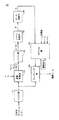
図1は、この発明の実施の形態に従う膜厚測定装置100の概略構成図である。
<Device configuration>
FIG. 1 is a schematic configuration diagram of a film
本実施の形態に従う膜厚測定装置100は、代表的に、単層または積層構造の被測定物における各層の膜厚を測定することが可能である。特に、本実施の形態に従う膜厚測定装置100は、比較的厚みの大きな層(代表的には、2μm〜1000μm)を含む被測定物の膜厚測定に適している。
Film
具体的には、膜厚測定装置100は、顕微分光式の測定装置であって、被測定物に光を照射し、当該被測定物で反射された反射光の波長分布特性(以下「スペクトル」とも称す。)に基づいて、被測定物を構成する各層の膜厚を測定可能である。なお、膜厚測定に限られず、各層における(絶対および相対)反射率の測定や層構造の解析も可能である。なお、反射光のスペクトルに代えて、被測定物を透過した光のスペクトル(透過光のスペクトル)を用いてもよい。
Specifically, the film
本明細書では、被測定物として、基板単体もしくは基板上に1つ以上の層が形成されたものを対象とする場合について例示する。被測定物の具体的な一例としては、Si基板、ガラス基板、サファイア基板などの比較的厚みのある基板単体や、SOI(Silicon on Insulator)基板のような積層構造の基板などである。特に、本実施の形態に従う膜厚測定装置100は、切削また研磨後のSi基板の膜厚、SOI基板のSi層(活性層)の膜厚、化学機械研磨(CMP)工程でのSi基板の膜厚などの測定に適している。
In this specification, the case where the object to be measured is a single substrate or a substrate on which one or more layers are formed is exemplified. Specific examples of the object to be measured include a relatively thick substrate such as a Si substrate, a glass substrate, and a sapphire substrate, and a substrate having a laminated structure such as an SOI (Silicon on Insulator) substrate. In particular, the film
図1を参照して、膜厚測定装置100は、測定用光源10と、コリメートレンズ12と、カットフィルタ14と、結像レンズ16,36と、絞り部18と、ビームスプリッタ20,30と、観察用光源22と、光ファイバ24と、出射部26と、ピンホールミラー32と、軸変換ミラー34と、観察用カメラ38と、表示部39と、対物レンズ40とステージ50と、可動機構51と、分光測定部60と、データ処理部70とを備える。
Referring to FIG. 1, a film
測定用光源10は、被測定物の反射率スペクトルを取得するために、所定の波長範囲をもつ測定光を発生する光源であり、特に赤外帯域に波長成分(たとえば、900nm〜1600nm、または1470nm〜1600nm)を有する光源が用いられる。測定用光源10としては、代表的にハロゲンランプが用いられる。
The
コリメートレンズ12と、カットフィルタ14と、結像レンズ16と、絞り部18とは、測定用光源10とビームスプリッタ30とを結ぶ光軸AX2上に配置され、測定用光源10から出射される測定光を光学的に調整する。
The collimating
具体的には、コリメートレンズ12は、測定用光源10からの測定光が最初に入射する光学部品であり、拡散光線として伝播する測定光を屈折させて平行光線に変換する。コリメートレンズ12を通過した測定光はカットフィルタ14に入射する。カットフィルタ14は、測定光に含まれる不要な波長成分を遮断する。代表的に、カットフィルタ14は、ガラス基板などに蒸着された多層膜によって形成される。結像レンズ16は、測定光のビーム径を調整するために、カットフィルタ14を通過した測定光を平行光線から収束光線に変換する。結像レンズ16を通過した測定光は絞り部18に入射する。絞り部18は、測定光の光量を所定量に調整した上でビームスプリッタ30へ出射する。好ましくは、絞り部18は、結像レンズ16によって変換された測定光の結像位置に配置される。なお、絞り部18の絞り量は、被測定物に入射する測定光の被写界深度や必要な光強度などに応じて適宜設定される。
Specifically, the collimating
一方、観察用光源22は、被測定物への焦点合わせや測定位置の確認に使用される観察光を生成する光源である。そして、観察用光源22が発生する観察光は、被測定物で反射可能な波長を含むように選択される。観察用光源22は、光ファイバ24を介して出射部26と接続されており、観察用光源22で生成された観察光は、光導波路である光ファイバ24を伝播した後に出射部26からビームスプリッタ20へ向けて出射される。
On the other hand, the observation
出射部26は、被測定物に所定の観察基準像が投射されるように、観察用光源22で生成された観察光の一部をマスクするマスク部26aを含む。この観察基準像は、その表面に何らの模様(パターン)も形成されていない被測定物(代表的に、透明なガラス基板など)に対しても、ユーザによる焦点合わせを容易化するためのものである。なお、レチクル像の形状はいずれであってもよいが、一例として同心円状や十字状のパターンなどを用いることができる。
The
すなわち、観察用光源22で生成された直後の観察光のビーム断面における光強度(光量)は略均一であるが、マスク部26aがこの観察光の一部をマスク(遮蔽)することで、観察光は、そのビーム断面において光強度が略ゼロである領域(影領域)が形成される。この影領域が観察基準像として被測定物に投射される。
That is, the light intensity (light quantity) in the beam cross section of the observation light immediately after being generated by the observation
ステージ50は、被測定物を配置するための試料台であり、その配置面は平坦に形成される。このステージ50は、一例として機械的に連結された可動機構51によって、3方向(X方向・Y方向・Z方向)に自在に駆動される。可動機構51は、代表的に3軸分のサーボモータと、各サーボモータを駆動するためのサーボドライバとを含んで構成される。そして、可動機構51は、ユーザまたは図示しない制御装置などからのステージ位置指令に応答してステージ50を駆動する。このステージ50の駆動によって、被測定物と後述する対物レンズ40との間の位置関係が変更される。
The
対物レンズ40と、ビームスプリッタ20と、ビームスプリッタ30と、ピンホールミラー32とは、ステージ50の平坦面に垂直な方向に延伸する光軸AX1上に配置される。
The
ビームスプリッタ30は、測定用光源10で生成される測定光を反射することで、その伝播方向を光軸AX1の紙面下向きに変換する。また、ビームスプリッタ30は、光軸AX1を紙面上向きに伝播する被測定物からの反射光を透過させる。
The
一方、ビームスプリッタ20は、観察用光源22で生成される観察光を反射することで、その伝播方向を光軸AX1の紙面下向きに変換する。同時に、ビームスプリッタ20は、光軸AX1を紙面下向きに伝播するビームスプリッタ30で反射された測定光を透過させる。すなわち、ビームスプリッタ20は、測定用光源10から集光光学系である対物レンズ40までの光学経路上の所定位置において観察光を注入する光注入部として機能する。このビームスプリッタ20で合成された測定光と観察光とは、対物レンズ40に入射する。また、ビームスプリッタ20は、光軸AX1を紙面上向きに伝播する被測定物からの反射光を透過させる。
On the other hand, the
特に、測定光は赤外帯域の波長成分を含み、観察光は可視帯域の波長成分を含むので、ビームスプリッタ20および30は、いずれもその透過/反射特性が可視帯域から赤外帯域まで所望の値を維持できるものが採用される。
In particular, since the measurement light includes a wavelength component in the infrared band and the observation light includes a wavelength component in the visible band, each of the
対物レンズ40は、光軸AX1を紙面下向きに伝播する測定光および観察光を集光するための集光光学系である。すなわち、対物レンズ40は、被測定物またはその近接した位置で結像するように測定光および観察光を収束させる。また、対物レンズ40は、所定の倍率(たとえば、10倍,20倍,30倍,40倍など)を有する拡大レンズであり、被測定物の光学特性を測定する領域を対物レンズ40に入射する光のビーム断面に比較してより微小化できる。
The
また、対物レンズ40から被測定物に入射した測定光および観察光は、被測定物で反射され、光軸AX1上を紙面上向きに伝播する。この反射光は、対物レンズ40に透過した後、ビームスプリッタ20および30を透過してピンホールミラー32まで到達する。
Further, the measurement light and the observation light incident on the measurement object from the
ピンホールミラー32は、被測定物で生じる反射光のうち、測定反射光と観察反射光とを分離する光分離部として機能する。具体的には、ピンホールミラー32は、光軸AX1を紙面上向きに伝播する被測定物からの反射光を反射する反射面を含み、その反射面と光軸AX1との交点を中心とする穴あき部(ピンホール)32aが形成されている。このピンホール32aの大きさは、測定用光源10からの測定光が被測定物で反射されて生じる測定反射光の、ピンホールミラー32の位置におけるビーム径に比較して小さくなるように形成される。また、このピンホール32aは、それぞれ測定光および観察光が被測定物で反射されて生じる測定反射光および観察反射光の結像位置と一致するように配置される。このような構成によって、被測定物で生じた反射光は、ピンホール32aを通過して分光測定部60に入射する。一方、反射光の残部は、その伝播方向を変換されて軸変換ミラー34へ入射する。
The
分光測定部60は、ピンホールミラー32を通過した測定反射光から反射率スペクトルを測定し、その測定結果をデータ処理部70へ出力する。より詳細には、分光測定部60は、回折格子(グレーティング)62と、検出部64と、カットフィルタ66と、シャッタ68とを含む。
The
カットフィルタ66と、シャッタ68と、回折格子62とは、光軸AX1上に配置される。カットフィルタ66は、ピンホールを通過して分光測定部60に入射する測定反射光に含まれる測定範囲外の波長成分を制限するための光学フィルタであり、特に測定範囲外の波長成分を遮断する。シャッタ68は、検出部64をリセットするときなどに、検出部64に入射する光を遮断するために使用される。シャッタ68は、代表的に電磁力によって駆動する機械式のシャッタからなる。
The
回折格子62は、入射する測定反射光を分光した上で、各分光波を検出部64へ導く。具体的には、回折格子62は、反射型の回折格子であり、所定の波長間隔毎の回折波が対応する各方向に反射するように構成される。このような構成を有する回折格子62に測定反射波が入射すると、含まれる各波長成分は対応する方向に反射されて、検出部64の所定の検出領域に入射する。なお、この波長間隔が分光測定部60における波長分解能に相当する。回折格子62は、代表的にフラットフォーカス型球面グレーティングからなる。
The
検出部64は、被測定物の反射率スペクトルを測定するために、回折格子62で分光された測定反射光に含まれる各波長成分の光強度に応じた電気信号を出力する。検出部64は、赤外帯域に感度をもつInGaAsアレイなどからなる。
The
データ処理部70は、検出部64によって取得された反射率スペクトルに対して、本発明に係る特徴的な処理を行うことで、被測定物を構成する各層の膜厚を測定する。さらに、データ処理部70は、被測定物の各層の反射率や層構造の解析も可能である。なお、このような処理の詳細については後述する。そして、データ処理部70は、測定した被測定物の膜厚をはじめとする光学特性を出力する。
The
一方、ピンホールミラー32で反射された観測反射光は光軸AX3に沿って伝播し、軸変換ミラー34へ入射する。軸変換ミラー34は、観測反射光の伝播方向を光軸AX3から光軸AX4に変換する。すると、観測反射光は、光軸AX4に沿って伝播し、観察用カメラ38へ入射する。
On the other hand, the observation reflected light reflected by the
観察用カメラ38は、観察反射光によって得られる反射像を取得する撮像部であり、代表的にはCCD(Charged Coupled Device)やCMOS(Complementary Metal Oxide Semiconductor)センサなどからなる。なお、観察用カメラ38は、代表的に可視帯域に感度をもつものであり、所定の測定範囲に感度をもつ検出部64とは異なる感度特性をもつ場合が多い。そして、観察用カメラ38は、観察反射光によって得られる反射像に応じた映像信号を表示部39へ出力する。表示部39は、観察用カメラ38からの映像信号に基づいて反射像を画面上に表示する。ユーザは、この表示部39に表示される反射像を目視して、被測定物に対する焦点合わせや測定位置の確認などを行う。表示部39は、代表的に液晶ディスプレイ(LCD)などからなる。なお、観察用カメラ38および表示部39に代えて、ユーザが反射像を直接的に目視できるファインダーを設けてもよい。
The
<反射光の解析的検討>
まず、被測定物に測定光を照射した場合に観測される反射光について、数学的および物理的に検討を行う。
<Analytical examination of reflected light>
First, the reflected light observed when the measurement object is irradiated with measurement light is studied mathematically and physically.
図2は、この発明の実施の形態に従う膜厚測定装置100が測定対象とする被測定物OBJの断面模式図の一例である。
FIG. 2 is an example of a schematic cross-sectional view of an object OBJ to be measured by the film
図2を参照して、被測定物OBJの代表例としてSOI基板を考える。すなわち、被測定物OBJは、Si層1とベースSi層3(基板層)との間にSiO2層2(BOX層)が配置された3層構造を有する。そして、膜厚測定装置100からの照射光は、紙面上側から被測定物OBJに入射するものとする。すなわち、測定光は、最初にSi層1へ入射するものとする。
With reference to FIG. 2, an SOI substrate is considered as a representative example of the object to be measured OBJ. That is, the DUT OBJ has a three-layer structure in which the SiO 2 layer 2 (BOX layer) is disposed between the
理解を容易にするために、被測定物OBJに入射した測定光がSi層1とSiO2層2との界面で反射して生じる反射光について考える。以下の説明では、添え字iを用いて各層を表現する。すなわち、空気や真空などの雰囲気層を添え字「0」、被測定物OBJのSi層1を添え字「1」、SiO2層2を添え字「2」とする。また、各層における屈折率を添え字iを用いて、屈折率niと表す。
In order to facilitate understanding, consider the reflected light that is generated when the measurement light incident on the object OBJ is reflected at the interface between the
互いに異なる屈折率niをもつ層の界面では光の反射が生じるため、屈折率の異なるi層とi+1層との間の各境界面でのP偏光成分およびS偏光成分の振幅反射率(Fresnel係数)r(P) i,i+1,r(S) i,i+1は次のように表わすことができる。 Since the reflection of light occurs at the interface of layers having different refractive indices n i to each other, P-polarized component and S amplitude reflectance of the polarization components at each interface between the different i-layer and the i + 1-layer refractive index (Fresnel Coefficients) r (P) i, i + 1 , r (S) i, i + 1 can be expressed as follows:

ここで、φiは、i層における入射角である。この入射角φiは、以下のようなSnellの法則によって、最上層の雰囲気層(0層)における入射角から計算できる。 Here, φ i is an incident angle in the i layer. This incident angle φ i can be calculated from the incident angle in the uppermost atmosphere layer (0 layer) according to Snell's law as follows.
N0sinφ0=Nisinφi
光が干渉可能な膜厚をもつ層内では、上式で表される反射率で反射する光が層内を何度も往復する。そのため、隣接する層との界面で直接反射した光と層内を多重反射した後の光との間ではその光路長が異なるため、位相が互いに異なったものとなり、Si層1の表面において光の干渉が生じる。このような、各層内における光の干渉効果を示すために、i層の層内における光の位相角βiを導入すると、以下のように表わすことができる。
N 0 sinφ 0 = N i sinφ i
In a layer having a film thickness that allows light interference, the light reflected at the reflectance expressed by the above formula reciprocates in the layer many times. For this reason, the optical path length differs between the light directly reflected at the interface with the adjacent layer and the light after multiple reflection within the layer, so that the phases are different from each other. Interference occurs. In order to show the light interference effect in each layer, when the phase angle β i of light in the i-layer is introduced, it can be expressed as follows.
ここで、diはi層の膜厚を示し、λは入射光の波長を示す。
より単純化するために、被測定物OBJに対して垂直に光が照射される場合、すなわち入射角φi=0とすると、P偏光とS偏光との区別はなくなり、各層間の界面における振幅反射率および薄膜の位相角β1は以下のようになる。
Here, d i denotes the film thickness of the i layer, lambda represents a wavelength of the incident light.
For further simplification, when light is irradiated perpendicularly to the object OBJ, that is, when the incident angle φ i = 0, there is no distinction between P-polarized light and S-polarized light, and the amplitude at the interface between the layers. The reflectance and the phase angle β 1 of the thin film are as follows.
さらに、図2に示す3層系の被測定物OBJにおける反射率Rは、以下のようになる。 Further, the reflectance R of the three-layer object to be measured OBJ shown in FIG. 2 is as follows.
上式において、位相角β1についての周波数変換(フーリエ変換)を考えると、位相因子(Phase Factor)であるcos2β1は反射率Rに対して非線形となる。そこで、この位相因子cos2β1について線形性を有する関数への変換を行う。一例として、この反射率Rを以下の式のように変換し、独自の変数である「波数変換反射率」R’を定義する。 In the above equation, considering frequency conversion (Fourier transform) for the phase angle β 1 , cos 2β 1 that is a phase factor is nonlinear with respect to the reflectance R. Therefore, to convert to a function having a linearity for the phase factor cos2β 1. As an example, the reflectance R is converted as shown in the following equation, and a unique variable “wave number conversion reflectance” R ′ is defined.
この波数変換反射率R’は、位相因子cos2β1についての1次式となり、線形性を有することになる。ここで、式中のRaは波数変換反射率R’における切片であり、Rbは波数変換反射率R’における傾きである。すなわち、この波数変換反射率R’は、各波長における反射率Rの値を周波数変換に係る位相因子cos2β1に対して線形化するための関数である。なお、このような位相因子について線形化するための関数としては、1/(1−R)という関数を用いてもよい。
This wave number conversion reflectance R ′ is a linear expression for the phase factor cos 2β 1 and has linearity. Here, R a in the equation is an intercept in the wave number conversion reflectance R ′, and R b is an inclination in the wave number conversion reflectance R ′. That is, the wave number conversion reflectance R ′ is a function for linearizing the value of the reflectance R at each wavelength with respect to the phase factor cos 2β 1 related to frequency conversion. As a function for linearizing such a phase factor, a
したがって、対象とするSi層1内の波数K1は以下のように定義できる。
Therefore, the wave number K 1 in the
ここで、Si層1内での波長λの光速度をsとし、真空中の波長λの光速度をcとすると、屈折率n1=c/sで表される。また、Si層1内をx方向に進行する光によって生じる電磁波E(x,t)は、波数K1,角周波数ω,位相δを用いて、E(x,t)=E0exp[j(ωt−K1x+δ)]と表される。すなわち、Si層1内の電磁波の伝搬特性は波数K1に依存する。これらの関係から、真空中において波長λをもつ光は、層内ではその光速度が低下するため、波長もλからλ/n1まで長くなることがわかる。このような波長分散現象を考慮して、波数変換反射率R’を以下のように定義する。
Here, when the light velocity of the wavelength λ in the
この関係から、波数変換反射率R’を波数Kについて周波数変換(フーリエ変換)すると、膜厚d1に相当する周期成分にピークが現れることにより、このピーク位置を特定することで、膜厚d1を算出することができる。 From this relationship, when the wave number conversion reflectance R ′ is frequency-converted (Fourier transform) for the wave number K, a peak appears in the periodic component corresponding to the film thickness d 1 , whereby the film thickness d is specified. 1 can be calculated.
すなわち、被測定物OBJから測定される反射率スペクトルと各波長における反射率との対応関係を、各波長から算出される波数と上述の関係式に従って算出される波数変換反射率R’との対応関係(波数分布特性)に変換し、この波数Kを含む波数変換反射率R’の関数を波数Kについて周波数変換し、この周波数変換後の特性に現れるピークに基づいて、被測定物OBJを構成するSi層1の膜厚を算出できる。これは、波数分布特性に含まれる各波数成分の振幅値を取得し、このうち振幅値の大きな波数成分に基づいて、Si層1の膜厚を算出することを意味する。なお、後述するように、波数分布特性から振幅値の大きな波数成分を解析する方法としては、FFT(Fast Fourier Transform:高速フーリエ変換)などの離散的なフーリエ変換を用いる方法と、最大エントロピー法(Maximum Entropy Method;以下、「MEM」とも称す。)などの最適化法を用いる方法とのいずれかを採用することができる。
That is, the correspondence between the reflectance spectrum measured from the object to be measured OBJ and the reflectance at each wavelength is the correspondence between the wave number calculated from each wavelength and the wave number conversion reflectance R ′ calculated according to the above relational expression. The relationship (wave number distribution characteristic) is converted, the function of the wave number conversion reflectance R ′ including the wave number K is frequency-converted with respect to the wave number K, and the object OBJ is configured based on the peak appearing in the characteristic after the frequency conversion. The film thickness of the
波数変換反射率R’の定義において、RaおよびRbは、層内における干渉現象とは無関係な値ではあるが、Si層1の屈折率n1を含む各層間の界面における振幅反射率に依存する。そのため、屈折率n1が波長分散をもつ場合には、その値は波長(すなわち、波数K)に依存する関数値となり、波数Kに関して一定値とはならない。そこで、フーリエ変換を⊃で表し、R’,Ra,Rb,cos2K1d1を波数Kでフーリエ変換した後の関数であるパワースペクトルをそれぞれP,Pa,Pb,Fとすると、以下の式が成立する。
In the definition of the wave number conversion reflectance R ′, R a and R b are values irrelevant to the interference phenomenon in the layer, but the amplitude reflectance at the interface between the layers including the refractive index n 1 of the
式中のPaにおける膜厚に依存する成分は相対的に小さく、かつパワースペクトルFとは独立のピークをもつので、パワースペクトルFに影響を与えない。 Component dependent on the film thickness at P a in the formula is relatively small, and since the power spectrum F with separated peaks, does not affect the power spectrum F.
一方、式中のPbは、パワースペクトルFとコンボリューションされることにより、Pbにおける膜厚成分がパワースペクトルFの膜厚成分に変調を加えることになる。しかしながら、Pbは、層内における干渉現象に無関係であり、隣接する2つの層における屈折率の波長依存性のみに影響を受けるため、波数Kに対するPbの膜厚成分はFの膜厚成分に比較して無視できる程度に小さい。たとえば、Rbが膜厚qの周期関数であるとし、そのフーリエ変換後のPbがコンボリューションによりパワースペクトルFの膜厚成分dに変調を加えたとすると、スペクトルとして現れるピークは、「d−q」または「d+q」となるが、qの値が非常に小さいのでピーク位置dに対する影響は小さい。 On the other hand, P b in the equation is convolved with the power spectrum F, so that the film thickness component in P b modulates the film thickness component of the power spectrum F. However, P b is independent of the interference phenomena in the layer, since it is affected only in the wavelength dependence of the refractive index in the two adjacent layers, the thickness component of P b for the wavenumber K is the thickness component of the F Is negligibly small compared to For example, assuming that R b is a periodic function of the film thickness q and P b after the Fourier transform is modulated on the film thickness component d of the power spectrum F by convolution, the peak appearing as the spectrum is “d− q ”or“ d + q ”, but since the value of q is very small, the influence on the peak position d is small.
さらに、フーリエ変換を行う際には、後述するように、測定対象の層の最大膜厚を考慮して、ナイキストのサンプリング定理に従って、波数変換反射率R’に対して適切なサンプル間隔およびサンプル数でサンプリングが行なわれる。このようにサンプリングされた波数変換反射率R’に基づいて算出されたパワースペクトルの膜厚分解能rに対して、Pbの膜厚成分qはより小さい可能性が高く(q<r)、膜厚dの測定結果にはほとんど影響を与えないといえる。 Further, when performing the Fourier transform, as will be described later, in consideration of the maximum film thickness of the layer to be measured, according to the Nyquist sampling theorem, an appropriate sample interval and number of samples with respect to the wave number conversion reflectivity R ′ Sampling is performed. Thus for a film thickness resolution r of the power spectrum calculated based on the sampled-wavenumber conversion reflectance R ', thickness component q of P b is high is less than possibility (q <r), film It can be said that the measurement result of the thickness d is hardly affected.
このように、算出された反射率スペクトルを、薄膜における波長分散を考慮した波数についての関数に変換した上で、フーリエ変換を行うことにより、薄膜の膜厚を正確に算出することができる。 Thus, the film thickness of the thin film can be accurately calculated by performing Fourier transform after converting the calculated reflectance spectrum into a function with respect to the wave number in consideration of wavelength dispersion in the thin film.
なお、上述の説明では、反射率スペクトルを用いる場合について例示したが、透過率スペクトルを用いてもよい。この場合には、測定された透過率をT、「波数変換透過率」をT’とすると、以下のような関係式で表される。 In the above description, the case where the reflectance spectrum is used is exemplified, but the transmittance spectrum may be used. In this case, when the measured transmittance is T, and the “wave number conversion transmittance” is T ′, the following relational expression is obtained.
透過率スペクトルを用いる場合においても、透過率Tは位相因子cos2β1に対して非線形となる。そのため、上述したのと同様の理由から、位相因子cos2β1について線形性を有する波数変換透過率T’を採用する。上式によれば、波数変換透過率T’は、位相因子cos2β1についての1次式となり、上述したのと同様の手順に従って、薄膜の膜厚を正確に算出することができる。すなわち、この波数変換透過率T’は、各波長における透過率Tの値を周波数変換に係る位相因子cos2β1に対して線形化するための関数である。 In the case of using the transmission spectra, the transmittance T becomes non-linear with respect to the phase factor cos2β 1. Therefore, for the same reason as described above, the wave number conversion transmittance T ′ having linearity with respect to the phase factor cos 2β 1 is adopted. According to the above equation, the wave number conversion transmittance T ′ is a linear equation for the phase factor cos 2β 1 , and the film thickness of the thin film can be accurately calculated according to the same procedure as described above. That is, the wave number conversion transmittance T ′ is a function for linearizing the value of the transmittance T at each wavelength with respect to the phase factor cos 2β 1 related to frequency conversion.
再度、図2を参照して、SiO2層2とベースSi層3との界面で反射して生じる反射光について考える。Si層1の屈折率をn1、膜厚をd1とし、SiO2層2の屈折率をn2、膜厚をd2とすると、波数変換反射率R’は以下のように表される。
With reference to FIG. 2 again, the reflected light generated by reflection at the interface between the SiO 2 layer 2 and the
ここで、Si層1の膜厚d1およびSiO2層2の膜厚d2を分離して算出する場合には、波数K1,K2でそれぞれ変換した波数変換反射率R1’(K1),R2’(K2)を用いる。具体的には、以下のように表される。
Here, when calculating separating the film thickness d 1 and the thickness d 2 of the SiO 2 layer 2 of
これらの式中において、d1’およびd2’は正しい膜厚ではないが、波数変換反射率R1’(K1)の第2項に相当するパワースペクトル中のピークから本来の膜厚d1を求めることができ、かつ波数変換反射率R2’(K2)の第3項に相当するパワースペクトル中のピークから本来の膜厚d2を求めることができる。 In these equations, d 1 ′ and d 2 ′ are not correct film thicknesses, but the original film thickness d from the peak in the power spectrum corresponding to the second term of the wave number conversion reflectance R 1 ′ (K 1 ). 1 and the original film thickness d 2 can be obtained from the peak in the power spectrum corresponding to the third term of the wave number conversion reflectance R 2 ′ (K 2 ).
なお、実際には、Si層1およびSiO2層2は、その屈折率が近似しており、両者の界面における反射率は、他の界面における反射率に比較して相対的に小さくなることが多い。その結果、波数変換反射率の関数に含まれるRbやRdに比較して、Rcの値が小さくなり、パワースペクトルから、波数変換反射率R2’(K2)の第3項に相当するピークを識別することが困難である場合も多い。このような場合には、波数変換反射率R2’(K2)の第4項に相当するパワースペクトルのピーク位置(d1’+d2)と、波数変換反射率R2’(K2)の第2項に相当するパワースペクトルのピーク位置(d1’)とを算出した上で、両者の差をとることで、膜厚d2を算出することができる。
Actually, the refractive index of the
<波長範囲および波長分解能について>
図3は、本実施の形態に従う膜厚測定装置100を用いてSOI基板を測定した場合の測定結果を示す図である。なお、図3には、測定光として、波長範囲が900〜1600nmであるものを用いた場合(図3(a))、および波長範囲が1340〜1600nmであるものを用いた場合(図3(b))の測定例を示す。なお、測定波長に応じて回折格子62を適切な特性を有するものを選択し、反射光が入射する検出部64(図1)での検出ポイント数(検出チャンネル数)はいずれも同一(たとえば、512チャンネル)であるとした。言い換えれば、波長範囲が狭いほど、検出ポイントあたりの波長間隔(すなわち、波長分解能)は小さくなる。
<About wavelength range and wavelength resolution>
FIG. 3 is a diagram showing a measurement result when an SOI substrate is measured using the film
上述の解析的検討によれば、測定される反射率は、波長に対して周期的に変化するはずである。 According to the analytical considerations described above, the measured reflectivity should vary periodically with wavelength.
図3(a)に示す測定結果においては、反射率が波長に対して周期的に変化している兆候は見られるものの、膜厚を測定するには十分な精度は得られていない。 In the measurement result shown in FIG. 3 (a), although there is an indication that the reflectance is periodically changed with respect to the wavelength, sufficient accuracy for measuring the film thickness is not obtained.
これに対して、図3(b)に示す測定結果においては、反射率のピークおよびバレイが明りょうに現れており、反射率の変化周期についても測定が可能となっている。図3(c)は、図3(b)に示される測定結果(反射率スペクトル)を上述した波数変換反射率R’の関数に変換した上で、波数Kについて周波数変換した結果を示す。この図3(c)に現れる主ピークに対応する値がSi層1の膜厚として決定できる。
On the other hand, in the measurement result shown in FIG. 3B, the reflectance peak and valley clearly appear, and the reflectance change period can also be measured. FIG. 3C shows the result of frequency conversion for the wave number K after the measurement result (reflectance spectrum) shown in FIG. 3B is converted into the function of the wave number conversion reflectance R ′ described above. A value corresponding to the main peak appearing in FIG. 3C can be determined as the film thickness of the
さらに、図4および図5には、SOI基板の別の測定結果を示す。
図4は、本実施の形態に従う膜厚測定装置100を用いてSOI基板を測定した別の測定結果を示す図である。図4には、Si層1の膜厚が10.0μm(設計値)であり、SiO2層2の膜厚が0.3μm(設計値)である場合の測定例を示す。また、図4(a)には、可視帯域(330〜1100nm)の波長成分をもつ測定光を用いた場合を示し、図4(b)には、赤外帯域(900〜1600nm)の波長成分をもつ測定光を用いた場合を示す。なお、上述したように、検出部64(図1)での検出ポイント数(検出チャンネル数)はいずれも同一である。
4 and 5 show other measurement results of the SOI substrate.
FIG. 4 is a diagram showing another measurement result obtained by measuring the SOI substrate using the film
図4(a)に示すように、可視帯域の波長成分をもつ測定光を用いた場合には、約860nmより長い波長領域では、反射率が周期的な挙動を示すものの、それより短い可視帯域では、有意な周期的変化を生じていないことがわかる。これに対して、図4(b)に示すように、赤外帯域の波長成分をもつ測定光を用いた場合には、反射率の周期的変化が有意に現れていることがわかる。 As shown in FIG. 4A, when measurement light having a wavelength component in the visible band is used, the reflectance exhibits a periodic behavior in a wavelength region longer than about 860 nm, but a shorter visible band than that. Thus, it can be seen that no significant periodic change has occurred. On the other hand, as shown in FIG. 4B, it can be seen that the periodic change in reflectance appears significantly when measurement light having a wavelength component in the infrared band is used.
また、図5は、本実施の形態に従う膜厚測定装置100を用いてSOI基板を測定したさらに別の測定結果を示す図である。図5には、Si層1の膜厚が80.0μm(設計値)であり、SiO2層2の膜厚が0.1μm(設計値)である場合の測定例を示す。また、図5(a)には、赤外帯域(900〜1600nm)の波長成分をもつ測定光を用いた場合を示し、図5(b)には、より狭い赤外帯域(1470〜1600nm)の波長成分をもつ測定光を用いた場合を示す。なお、上述したように、検出部64(図1)での検出ポイント数(検出チャンネル数)はいずれも同一である。
FIG. 5 is a diagram showing still another measurement result obtained by measuring the SOI substrate using film
図5(a)に示すように、赤外帯域の波長成分をもつ測定光を用いた場合であっても、測定された反射率には有意な周期的変化が現れていないことがわかる。これに対して、図5(b)に示すように、より狭い赤外帯域の波長成分をもつ測定光を用いた場合には、反射率の周期的変化が有意に現れていることがわかる。 As shown in FIG. 5A, it can be seen that even when measurement light having a wavelength component in the infrared band is used, no significant periodic change appears in the measured reflectance. On the other hand, as shown in FIG. 5B, it can be seen that when measuring light having a narrower wavelength component in the infrared band is used, a periodic change in reflectance appears significantly.
以上の測定例によれば、比較的厚みのある層の膜厚を高い精度で測定するためには、測定光の波長範囲および波長分解能を適切に設定する必要があるといえる。これは、層内での光干渉現象を利用する測定方法であること、および検出部64による反射光の波長分解能が有限であることに起因するものであり、以下に説明するような手順によって、適切な測定光の波長を設定することが好ましい。
According to the above measurement examples, it can be said that it is necessary to appropriately set the wavelength range and wavelength resolution of the measurement light in order to measure the film thickness of the relatively thick layer with high accuracy. This is due to the fact that it is a measurement method that utilizes the optical interference phenomenon in the layer and that the wavelength resolution of the reflected light by the
以下の検討では、膜厚測定範囲の下限値をdminとし、膜厚測定範囲の上限値をdmaxとする。また、検出部64の波長検出の下限値をλminとし、検出部64の波長検出の上限値をλmaxとする。なお、測定用光源10(図1)が照射する測定光の波長範囲は、検出部64の波長検出範囲を含むものであれば、いずれの範囲であってもよい。さらに、検出部64(図1)での検出ポイント数(検出チャンネル数)をSpとする。
In the following discussion, the lower limit value of the film thickness measurement range is d min and the upper limit value of the film thickness measurement range is d max . Further, the lower limit value of the wavelength detection of the
図6は、この発明の実施の形態に従う膜厚測定範囲と検出部64の検出波長範囲および検出ポイント数との関係を説明するための図である。
FIG. 6 is a diagram for explaining the relationship between the film thickness measurement range, the detection wavelength range of the
(1)膜厚測定範囲の下限値dminと検出波長範囲との関係
上述した膜厚の測定方法によれば、対象の被測定物内で光干渉を生じる波長を見つける必要があるので、検出部64が光干渉を生じ得る波長範囲をもつ必要がある。すなわち、図6(a)に示すように、被測定物に対して測定される反射率波形が検出部64の検出波長範囲において1周期以上変化する必要がある。
(1) Relationship between the lower limit d min of the film thickness measurement range and the detection wavelength range According to the above-described film thickness measurement method, it is necessary to find the wavelength that causes optical interference in the object to be measured. The
これは、検出部64の検出波長範囲が下限値λminから上限値λmaxまで変化することで生じる光学的距離が被測定物の膜厚の往復分以上変化する必要があることを意味する。したがって、膜厚測定範囲の下限値dminと測定光の波長範囲との関係としては、以下の条件式(1)を満たす必要がある。
This means that the optical distance generated when the detection wavelength range of the
(2)膜厚測定範囲の上限値dmaxと検出ポイント数との関係
図6(b)に示すように、測定光の波長が長くなるほど、被測定物に対して測定される反射率波形の周期は長くなる。図6(c)に示す反射率波形は、図6(b)に示す反射率波形を波数(1/f)の座標に変換したものである。このとき、InGaAsなどの各アレイ素子が波長について等間隔に配置されているとすると、波数に対する各アレイ素子の配置間隔は波数が小さくなるほど広がることがわかる。
(2) Relationship between the upper limit d max of the film thickness measurement range and the number of detection points As shown in FIG. 6 (b), the longer the wavelength of the measurement light, the higher the reflectance waveform measured for the object to be measured. The period becomes longer. The reflectance waveform shown in FIG. 6 (c) is obtained by converting the reflectance waveform shown in FIG. 6 (b) into coordinates of wave number (1 / f). At this time, if the array elements such as InGaAs are arranged at equal intervals with respect to the wavelength, it can be seen that the arrangement interval of the array elements with respect to the wave number increases as the wave number decreases.
したがって、波数に対して所定の周期で変化する反射率波形を正確にサンプリングするためには、この各アレイ素子の配置間隔(波長分解能Δλ)がナイキストのサンプリング定理を満たす必要があり、このサンプリング定理が満たされるという条件によって、膜厚測定範囲の上限値dmaxが決定される。 Therefore, in order to accurately sample a reflectance waveform that changes with a predetermined period with respect to the wave number, the arrangement interval (wavelength resolution Δλ) of each array element must satisfy the Nyquist sampling theorem. Is satisfied, the upper limit value d max of the film thickness measurement range is determined.
検出部64における波長分解能Δλは、検出ポイント数(検出チャンネル数)Spを用いて、Δλ=(λmax−λmin)/Spと表わすことができる。
Wavelength resolution [Delta] [lambda] in the
測定光の波長が長くなるほど反射率波形の周期は短くなるので、反射率波形において測定光の上限値λmaxにおいて極値(ピークまたはバレイ)が生じるとした場合に、当該極値と隣接する極値(ピークに隣接するピーク、またはバレイに隣接するバレイ)を生じる波長をλ1とすると、膜厚測定範囲の上限値dmaxとの間に、以下の条件が満たされる必要がある。 The longer the wavelength of the measurement light, the shorter the period of the reflectance waveform. Therefore, when an extreme value (peak or valley) occurs at the upper limit value λ max of the measurement light in the reflectance waveform, the extreme adjacent to the extreme value is generated. and the wavelength that occurs the value (peak adjacent to the peak or valley adjacent to the valley) and lambda 1, between the upper limit value d max of the film thickness measurement range it is necessary for the following conditions are met.
ここで、測定対象の層の膜厚が比較的大きな場合には、nmax≒n1とみなすことができるので、上述の条件は、以下のような条件式(2)として表わすことができる。 Here, when the thickness of the layer to be measured is relatively large, it can be considered that n max ≈n 1, and thus the above-described condition can be expressed as the following conditional expression (2).
このとき、波長分解能Δλについては、以下の条件が満たされる必要がある。 At this time, the following conditions must be satisfied for the wavelength resolution Δλ.
上述の波長分解能Δλの関係式に、上限値dmaxの関係式を代入してλ1の項をなくすと、以下のような条件式(3)として表わすことができる。 The relationship of the above-described wavelength resolution [Delta] [lambda], the elimination of the upper limit value d max assignment to lambda 1 in terms of the relational expression, can be expressed as the following conditions (3).
以上の検討の結果、被測定物について要求される膜厚測定範囲(下限値dmin〜上限値dmax)が予め定められると、上述の条件式(1)および(2)を満足するように、測定光の波長範囲(下限値λmin〜上限値λmax)および検出ポイント数Spを定める必要がある。 As a result of the above examination, when the film thickness measurement range (lower limit value d min to upper limit value d max ) required for the object to be measured is determined in advance, the above conditional expressions (1) and (2) are satisfied. , it is necessary to determine the wavelength range (lower limit lambda min ~ limit lambda max) and the detection points S p of the measurement light.
<計算例>
図2に示すようなSOI基板のSi層1の膜厚を測定する場合に必要とされる条件について計算した一例を以下に示す。
<Calculation example>
An example of calculating the conditions required for measuring the film thickness of the
この計算例では、SOI基板のSi層1の上限値dmaxが100μmであるとし、屈折率nが波長に依らず一定値(n=3.5)であるとした。なお、この計算例では、SOI基板のSi層1の下限値dminについては考慮していない。
In this calculation example, the upper limit d max of the
上記の前提となる値を上述のそれぞれの条件式(2)および(3)に代入すると、上限値λmax=1424.0nm、波長分解能Δλ=1.445375nmと算出される。したがって、最大100μmの膜厚をもつ被測定物の膜厚測定を行うために、512チャンネルの検出部64を用いた場合には、約684〜1424nmの波長範囲を含む測定光を用いて、検出部64で当該範囲の反射光を検出(波長分解能Δλ=1.4453125nm)すればよいことがわかる。
Substituting the above-mentioned presupposed values into the respective conditional expressions (2) and (3), the upper limit value λ max = 1424.0 nm and the wavelength resolution Δλ = 1.445375 nm are calculated. Therefore, when the 512-
但し、上記の条件式によって算出される波長分解能Δλは、理論上の最低限のスペックを記述したものであり、実際に測定を行う場合には、算出された波長分解能Δλに比較して精度をより高くすることが好ましい。なお、より好ましくは、数倍程度(たとえば、2〜4倍)にすることがよい。なお、精度を高くすることは、波長分解能Δλの値をより小さく設定することを意味する。 However, the wavelength resolution Δλ calculated by the above conditional expression describes the minimum theoretical specifications. When actually measuring, the accuracy is compared with the calculated wavelength resolution Δλ. It is preferable to make it higher. More preferably, it should be several times (for example, 2 to 4 times). Increasing the accuracy means setting the wavelength resolution Δλ to be smaller.
すなわち、実際の膜厚測定装置では、被測定物への測定光の入射角の影響や、レンズ集光系を用いたときの開口角の影響などによって、スペクトル精度が劣化する場合がある。このような場合には、パワースペクトル上のピーク高さが小さくなり、膜厚の算出が困難になる。また、有限個のサンプリング値を用いて離散的に周波数変換を行うFFTなどを用いた場合には、エリアシングの影響を受けて、波数変換時などの変換誤差が大きく生じる場合もある。さらに、被測定物の屈折率分散が測定光の波長範囲によっては大きく変化するものもあり、部分的に条件に合致しない可能性もある。 That is, in an actual film thickness measurement apparatus, the spectral accuracy may be deteriorated due to the influence of the incident angle of the measurement light on the object to be measured, the influence of the aperture angle when the lens focusing system is used, or the like. In such a case, the peak height on the power spectrum becomes small, making it difficult to calculate the film thickness. In addition, when an FFT that performs frequency conversion discretely using a finite number of sampling values is used, there may be a large conversion error due to the effect of aliasing. Furthermore, the refractive index dispersion of the object to be measured varies greatly depending on the wavelength range of the measurement light, and may not partially meet the conditions.
図7は、理論値に近い波長分解能をもつ膜厚測定装置を用いて測定した結果をシミュレーションした結果を示す図である。図8は、理論値に対して精度を2倍にした波長分解能をもつ膜厚測定装置を用いて測定した結果をシミュレーションした結果を示す図である。なお、対象とする被測定物の膜厚は100μmであるとした。 FIG. 7 is a diagram showing the result of simulating the result of measurement using a film thickness measuring device having a wavelength resolution close to the theoretical value. FIG. 8 is a diagram showing a result of simulating a result of measurement using a film thickness measuring apparatus having a wavelength resolution in which accuracy is doubled with respect to a theoretical value. Note that the film thickness of the object to be measured was 100 μm.
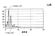
より具体的には、図7(a)には、512チャンネルの検出部64を用いて、900nm〜1600nmの範囲で反射率スペクトルを測定(波長分解能Δλ=2.734375nm)した結果を示し、図7(b)には、図7(a)に示す反射率スペクトルを周波数変換(ここでは、FFT変換)したパワースペクトルを示す。図7(b)に示すように、この場合には、100μmの付近にピークが存在しているものの、薄膜側のノイズ(ゴースト)に比較してそのレベルは小さく、膜厚の決定が難しい場合もある。
More specifically, FIG. 7A shows the result of measuring the reflectance spectrum in the range of 900 nm to 1600 nm (wavelength resolution Δλ = 2.734375 nm) using the 512-
一方、図8(a)には、検出部64における波長分解能の精度が理論値の2倍となるように波長範囲を定めた場合の測定結果を示し、図8(b)には、図8(a)に示す反射率スペクトルを周波数変換(ここでは、FFT変換)したパワースペクトルを示す。この例では、検出部64の波長分解能Δλが1.3671875nmとなるように、検出ポイント数および波長範囲を定めている。図8(b)に示すように、この場合には、本来の膜厚である100μmの付近に強いピークが現れており、被測定物の膜厚を正確に測定できることを意味している。
On the other hand, FIG. 8A shows a measurement result when the wavelength range is determined so that the wavelength resolution accuracy in the
<膜厚算出処理の概要>
上述したように、被測定物の膜厚は、反射率スペクトルの周期性に基づいて算出することができる。すなわち、検出された反射率スペクトルを周波数変換してパワースペクトルを求め、このパワースペクトルに現れるピークから膜厚を算出できる。このようなパワースペクトルは、現実的にはFFTなどの離散的なフーリエ変換法によって算出される。しかしながら、FFTでは周期性を十分に反映したパワースペクトルを得られない場合もある。そのため、本実施の形態に従う膜厚測定装置100は、パワースペクトルの算出方法として、FFTなどの離散的なフーリエ変換に加えて、MEMなどの最適化法を実行可能に構成される。すなわち、本実施の形態に従う膜厚測定装置100は、検出された反射率スペクトルに応じて、フーリエ変換および最適化法を選択的または併合的に実行する。なお、MEMの処理の詳細については、「科学計測のための波形データ処理 計測システムにおけるマイコン/パソコン活用技術」、南茂夫編著、CQ出版社、1992年8月1日第10版発行などに詳しいので、そちらを参照されたい。
<Outline of film thickness calculation process>
As described above, the film thickness of the object to be measured can be calculated based on the periodicity of the reflectance spectrum. That is, the detected reflectance spectrum is frequency converted to obtain a power spectrum, and the film thickness can be calculated from the peak appearing in the power spectrum. Such a power spectrum is actually calculated by a discrete Fourier transform method such as FFT. However, in some cases, FFT cannot obtain a power spectrum that sufficiently reflects periodicity. Therefore, film
さらに、本実施の形態に従う膜厚測定装置100は、上述したような検出された反射率スペクトルから解析的に膜厚を算出する方法に加えて、測定対象から算出される物理モデルから理論的に算出される反射率スペクトルと実際に検出された反射率スペクトルとの偏差に基づいて、測定対象の光学的特性値を探索的に算出する、いわゆるフィッティングと称される方法も実行可能に構成される。
Furthermore, in addition to the method for analytically calculating the film thickness from the detected reflectance spectrum as described above, the film
ところで、図2に示すSOI基板のように、第2層であるSiO2層2の膜厚に比較して、第1層のSi層1の膜厚が2桁以上大きいような被測定物については、フィッティング法では各層の膜厚を十分な精度で算出できない場合もある。
By the way, as shown in FIG. 2, an object to be measured in which the film thickness of the
図9は、SOI基板についての反射率スペクトルの測定結果を示す図である。図9には、第1層のSi層1の膜厚が100μmであり、第2層であるSiO2層2の膜厚を0.48〜0.52μmの範囲で0.1μm刻みで変化させた場合の測定例を示す。図9に示されているように、第2層であるSiO2層2の膜厚が変化しても、測定される反射率スペクトルにはあまり大きな変化が生じていないことがわかる。すなわち、このような被測定物から測定される反射率スペクトルでは、第1層のSi層1の影響が主体的であるため、第2層であるSiO2層2のパラメータを変化させたとしても、十分にフィッティングできないことを意味する。
FIG. 9 is a diagram showing the measurement results of the reflectance spectrum for the SOI substrate. In FIG. 9, the thickness of the
そこで、本実施の形態に従う膜厚測定装置100は、SOI基板などのように、異なる複数の層を有する被測定物について、各層の膜厚を独立して正確に解析できるように、上述したフーリエ変換、最適化法、フィッティング法のうちいずれか1つ、もしくは複数を適宜組み合わせて実行する。以下、本実施の形態に従う膜厚測定装置100における膜厚算出処理の詳細について説明する。なお、このような膜厚算出処理は、データ処理部70(図1)によって実行される。
Therefore, the film
<データ処理部の構成>
図10は、この発明の実施の形態に従うデータ処理部70の概略のハードウェア構成を示す模式図である。
<Configuration of data processing unit>
FIG. 10 is a schematic diagram showing a schematic hardware configuration of
図10を参照して、データ処理部70は、代表的にコンピュータによって実現され、オペレーティングシステム(OS:Operating System)を含む各種プログラムを実行するCPU(Central Processing Unit)200と、CPU200でのプログラムの実行に必要なデータを一時的に記憶するメモリ部212と、CPU200で実行されるプログラムを不揮発的に記憶するハードディスク部(HDD:Hard Disk Drive)210とを含む。また、ハードディスク部210には、後述するような処理を実現するためのプログラムが予め記憶されており、このようなプログラムは、フレキシブルディスクドライブ(FDD)216またはCD−ROMドライブ214によって、それぞれフレキシブルディスク216aまたはCD−ROM(Compact Disk-Read Only Memory)214aなどから読み取られる。
Referring to FIG. 10,
CPU200は、キーボードやマウスなどからなる入力部208を介してユーザなどからの指示を受取るとともに、プログラムの実行によって測定される測定結果などをディスプレイ部204へ出力する。各部は、バス202を介して互いに接続される。
The
<演算処理構造>
本実施の形態に従うデータ処理部70は、被測定物の各層のパラメータ(材質、膜厚、膜厚範囲、屈折率、消衰係数など)のうち未知の値の種類や数、および解析精度などに応じて、以下に示す処理パターン1〜6のいずれかを選択して実行することが可能である。なお、以下の説明では、図2に示すSOI基板のように、積層された2層(それぞれ「第1層」および「第2層」とも称す。)の膜厚をそれぞれ独立に算出する場合について例示するが、同様の手順によって、より多くの積層された膜厚をそれぞれ独立に算出することが可能である。
<Operation processing structure>
The
(1)処理パターン1
処理パターン1は、第1層および第2層の屈折率および消衰係数が既知である場合に実行可能な膜厚算出処理である。この処理パターン1では、各層の膜厚はいずれもフィッティング法によって決定される。なお、フィッティング法として、代表的に、最小二乗法を用いる場合について例示する。
(1)
The
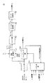
図11は、この発明の実施の形態に従う処理パターン1に係る膜厚算出処理を実行する制御構造を示すブロック図である。図11に示すブロック図は、CPU200がハードディスク部210などの予め格納されたプログラムをメモリ部212などに読み出して実行することで実現される。
FIG. 11 is a block diagram showing a control structure for executing the film thickness calculation process according to
図11を参照して、データ処理部70(図1)は、バッファ部71と、モデル化部721と、フィッティング部722とをその機能として含む。
Referring to FIG. 11, data processing unit 70 (FIG. 1) includes a
バッファ部71は、分光測定部60(図1)から出力される実測された反射率スペクトルR(λ)を一時的に格納する。より具体的には、分光測定部60からは所定の波長分解能毎に反射率の値が出力されるので、バッファ部71は、波長とその波長における反射率とを対応付けて格納する。
The
モデル化部721は、被測定物に係るパラメータを受付けて、当該受付けたパラメータに基づいて、被測定物における理論反射率を示すモデル式(関数)を決定し、当該決定した関数に従って、各波長における理論反射率(スペクトル)を算出する。この算出した各波長における理論反射率は、フィッティング部722へ出力される。より具体的には、モデル化部721は、第1層の屈折率n1および消衰係数k1と、第2層の屈折率n2および消衰係数k2とを受付けるとともに、第1層の膜厚d1の初期値および第2層の膜厚d2の初期値を受付ける。なお、ユーザが各パラメータを入力してもよいが、予め標準的な材質のパラメータをファイルなどとして格納しておき、必要に応じて読出すようにしてもよい。また、必要に応じて、雰囲気層の屈折率n0および消衰係数k0についても入力される。
The
理論反射率を示すモデル式については、上述した3層系の被測定物OBJにおける反射率Rと同様であり、少なくとも各層の膜厚の値を含む関数となる。 The model expression indicating the theoretical reflectance is the same as the reflectance R in the above-described three-layer object to be measured OBJ, and is a function including at least the value of the film thickness of each layer.
また、モデル化部721は、後述するフィッティング部722からのパラメータ更新指令に従って、理論反射率を示す関数を更新し、更新後の関数に従って、各波長における理論反射率(スペクトル)を繰返し算出する。より具体的には、モデル化部721は、パラメータとして、第1層の膜厚d1および第2層の膜厚d2を順次更新する。
In addition, the
フィッティング部722は、バッファ部71から反射率スペクトルの実測値を読出し、モデル化部721から出力される反射率スペクトルの理論値との間の二乗偏差を各波長について順次算出する。そして、フィッティング部722は、各波長における偏差から残差を算出し、この残差が所定のしきい値以下であるか否かを判断する。すなわち、フィッティング部722は、現時点のパラメータにおいて収束しているか否かを判断する。
The
残差が所定のしきい値以下でなければ、フィッティング部722は、モデル化部721に対してパラメータ更新指令を与え、新たに反射率スペクトルの理論値が出力されるまで待つ。一方、残差が所定のしきい値以下であれば、フィッティング部722は、現時点の第1層の膜厚d1および第2層の膜厚d2を解析値として出力する。
If the residual is not less than the predetermined threshold value, the
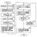
図12は、この発明の実施の形態に従う処理パターン1に係る膜厚算出処理の手順を示すフローチャートである。
FIG. 12 is a flowchart showing a procedure of film thickness calculation processing according to
図12を参照して、まず、ユーザが被測定物(試料)をステージ50(図1)上に配置する(ステップS100)。続いて、ユーザが測定準備指令を与えると、観察用光源22(図1)からは観察光の照射が開始される。ユーザは、表示部39に表示される観察用カメラ38で撮影された反射像を参照しながら、可動機構51にステージ位置指令を与えて、測定範囲の調整や焦点合わせを行う(ステップS102)。
Referring to FIG. 12, the user first places an object to be measured (sample) on stage 50 (FIG. 1) (step S100). Subsequently, when the user gives a measurement preparation command, observation light irradiation is started from the observation light source 22 (FIG. 1). The user gives a stage position command to the
測定範囲の調整や焦点合わせの完了後、ユーザが測定開始指令を与えると、測定用光源10(図1)から測定光の発生が開始される。分光測定部60は、被測定物からの反射光を受光し、当該反射光に基づく反射率スペクトルをデータ処理部70へ出力する(ステップS104)。続いて、データ処理部70のCPU200は、分光測定部60で検出された反射率スペクトルをメモリ部212などに一時的に格納する(ステップS106)。その後、データ処理部70のCPU200が以下に示す膜厚算出処理を実行する。
When the user gives a measurement start command after the adjustment of the measurement range and the focus adjustment, generation of measurement light from the measurement light source 10 (FIG. 1) is started. The
CPU200は、ディスプレイ部204(図2)などに入力画面を表示して、ユーザにパラメータの入力を促す(ステップS108)。ユーザは、表示された入力画面上などから、被測定物の第1層の屈折率n1および消衰係数k1と、被測定物の第2層の屈折率n2および消衰係数k2とを入力するとともに、被測定物に係る第1層の膜厚d1および第2層の膜厚d2の初期値を入力する(ステップS110)。
The
さらに、CPU200は、ユーザ入力されたパラメータに基づいて、反射率スペクトルの理論値を算出する(ステップS112)。続いて、CPU200は、メモリ部212などに格納されている反射率スペクトルの実測値と反射率スペクトルの理論値との間の二乗偏差を各波長について順次算出し、両者の間の残差を算出する(ステップS114)。さらに、CPU200は、算出した残差が所定のしきい値以下であるか否かを判断する(ステップS116)。
Further, the
算出した残差が所定のしきい値以下でない場合(ステップS116においてNOの場合)には、CPU200は、第1層の膜厚d1および第2層の膜厚d2の現在値を変更する(ステップS118)。なお、膜厚d1およびd2をどの方向にどの程度変更するかについては、残差の発生度合いに応じて決定される。そして、処理はステップS112に戻る。
When the calculated residual is not less than a predetermined threshold value (NO in step S116), the
これに対して、算出した残差が所定のしきい値以下である場合(ステップS116においてYESの場合)には、CPU200は、第1層の膜厚d1および第2層の膜厚d2の現在値を被測定物の各層の膜厚(解析値)として出力する(ステップS120)。そして、処理は終了する。
On the contrary, when the calculated residual is equal to or smaller than the predetermined threshold (YES in step S116), the
なお、図11に示すブロック図では、屈折率n1,n2および消衰係数k1,k2として固定値を入力する構成について例示したが、波長分散を考慮した屈折率および消衰係数を用いてもよい。たとえば、波長分散を考慮した屈折率および消衰係数としては、以下に示すようなCauchyモデルの式を用いてもよい。 In the block diagram shown in FIG. 11, the configuration in which fixed values are input as the refractive indexes n 1 and n 2 and the extinction coefficients k 1 and k 2 is illustrated. However, the refractive index and the extinction coefficient in consideration of wavelength dispersion are illustrated. It may be used. For example, the following Cauchy model equation may be used as the refractive index and extinction coefficient considering wavelength dispersion.
このような式を用いる場合には、式中の各係数についても予め初期値または既知の値を入力しておき、これらの係数についてもフィッティング対象とされる。 When such an expression is used, an initial value or a known value is input in advance for each coefficient in the expression, and these coefficients are also subject to fitting.
あるいは、以下に示すようなSellmeierモデルの式を用いてもよい。 Alternatively, the following Sellmeier model formula may be used.
(2)処理パターン2
処理パターン2は、第1層および第2層の屈折率および消衰係数が既知である場合に実行可能な膜厚算出処理である。この処理パターン2では、膜厚の大きい第1層を離散的なフーリエ変換を用いた周波数変換によって求め、この第1層の膜厚を固定値として、第2層の膜厚をフィッティング法によって決定する。なお、フィッティング法として、代表的に、最小二乗法を用いる場合について例示する。
(2)
The
図13は、この発明の実施の形態に従う処理パターン2に係る膜厚算出処理を実行する制御構造を示すブロック図である。図13に示すブロック図は、CPU200がハードディスク部210などの予め格納されたプログラムをメモリ部212などに読み出して実行することで実現される。
FIG. 13 is a block diagram showing a control structure for executing a film thickness calculation process according to
図13を参照して、データ処理部70(図1)は、バッファ部71と、波数変換部731と、バッファ部732と、フーリエ変換部733と、ピーク探索部734と、モデル化部735と、フィッティング部736とをその機能として含む。
Referring to FIG. 13, the data processing unit 70 (FIG. 1) includes a
バッファ部71は、分光測定部60(図1)から出力される実測された反射率スペクトルR(λ)を一時的に格納する。なお、その具体的な構成に処理内容については、上述したので詳細な説明は繰返さない。
The
波数変換部731は、第1層に係るパラメータ(屈折率n1および消衰係数k1)を受付けて、当該受付けたパラメータに基づいて、バッファ部71に一時的に格納される反射率スペクトルR(λ)を波数変換する。すなわち、波数変換部731は、反射率スペクトルR(λ)における各波長とその波長における反射率との対応関係を、各波長についての波数K1(λ)と上述の関係式に従って算出される対応の波数変換反射率R1’との対応関係に変換する。より具体的には、波数変換部731は、バッファ部71に格納される波長毎に、波数K1(λ)および波数変換反射率R1’(λ)(=R(λ)/(1−R(λ)))を順次算出し、バッファ部732へ出力する。
The wave
バッファ部732は、波数変換部731から順次出力される波数K1(λ)と波数変換反射率R1’(λ)とを対応付けて格納する。すなわち、バッファ部732には、波数K1(λ)に関する波数変換反射率の波数分布特性である波数変換反射率R1’(K1)が格納される。
The
フーリエ変換部733は、バッファ部732に格納される波数変換反射率R1’(K1)を波数K1についてフーリエ変換を行って、パワースペクトルP1を算出する。なお、フーリエ変換の方法としては、高速フーリエ変換(FFT)や離散コサイン変換(DCT:Discrete Cosine Transform)などを用いることができる。
The
ピーク探索部734は、フーリエ変換部733によって算出されたパワースペクトルP1の中に現れるピークを探索し、当該ピークに対応する膜厚を取得し、第1層の膜厚d1として出力する。
モデル化部735は、被測定物に係るパラメータを受付けて、当該受付けたパラメータに基づいて、被測定物における理論反射率を示すモデル式(関数)を決定し、当該決定した関数に従って、各波長における理論反射率(スペクトル)を算出する。この算出した各波長における理論反射率は、フィッティング部736へ出力される。より具体的には、モデル化部735は、ピーク探索部734から出力される第1層の膜厚d1と、第2層の屈折率n2および消衰係数k2とを受付けるとともに、第2層の膜厚d2の初期値を受付ける。なお、ユーザが各パラメータを入力してもよいが、予め標準的な材質のパラメータをファイルなどとして格納しておき、必要に応じて読出すようにしてもよい。理論反射率を示すモデル式については、上述した3層系の被測定物OBJにおける反射率Rと同様であり、少なくとも各層の膜厚の値を含む関数となる。
The
また、モデル化部735は、フィッティング部736からのパラメータ更新指令に従って、理論反射率を示す関数を更新し、更新後の関数に従って、各波長における理論反射率(スペクトル)を再度算出する。より具体的には、モデル化部735は、パラメータとして、第2層の膜厚d2を順次更新する。
In addition, the
フィッティング部736は、バッファ部71から反射率スペクトルの実測値を読出し、モデル化部735から出力される反射率スペクトルの理論値との間の二乗偏差を各波長について順次算出する。そして、フィッティング部736は、各波長における偏差から残差を算出し、この残差が所定のしきい値以下であるか否かを判断する。すなわち、フィッティング部736は、現時点のパラメータにおいて収束しているか否かを判断する。
The
残差が所定のしきい値以下でなければ、フィッティング部736は、モデル化部735に対してパラメータ更新指令を与え、新たに反射率スペクトルの理論値が出力されるまで待つ。一方、残差が所定のしきい値以下であれば、フィッティング部736は、現時点の第1層の膜厚d1および第2層の膜厚d2を解析値として出力する。
If the residual is not less than the predetermined threshold value, the
図14は、この発明の実施の形態に従う処理パターン2に係る膜厚算出処理の手順を示すフローチャートである。図14に示すフローチャートの各ステップのうち、ステップS100〜S108の処理については、図12に示すフローチャートの同一符号を付した各ステップと同様であるので、詳細な説明は繰返さない。以下、図12に示すフローチャートと異なるステップS132以降の膜厚算出処理について説明する。
FIG. 14 is a flowchart showing a procedure of film thickness calculation processing according to
ステップS132において、ユーザは、表示された入力画面上などから、被測定物の第1層の屈折率n1および消衰係数k1、ならびに被測定物の第2層の屈折率n2および消衰係数k2を入力するとともに、第2層の膜厚d2の初期値を入力する。 In step S132, the user, or the like displayed input screen, the refractive index n 1 and the extinction coefficient k 1 of the first layer of the object to be measured, and the refractive index n 2 and the extinction of the second layer of the object to be measured You input the coefficient of k 2, and inputs the initial value of the film thickness d 2 of the second layer.
すると、CPU200は、入力された第1層の屈折率n1および消衰係数k1に基づいて、メモリ部212などに格納されている反射率スペクトルを波数変換する(ステップS134)。そして、CPU200は、この波数変換して得られる波数変換反射率をメモリ部212などに格納する(ステップS136)。さらに、CPU200は、波数変換反射率を波数K1についてフーリエ変換を行って、パワースペクトルを算出する(ステップS138)。さらに、CPU200は、算出したパワースペクトルに現れるピークおよびそのピークに対応する膜厚を第1層の膜厚d1として取得する(ステップS140)。
Then, the
続いて、CPU200は、ステップS210で取得された第1層の膜厚d1と、ユーザ入力された第2層に係るパラメータとに基づいて、反射率スペクトルの理論値を算出する(ステップS142)。そして、CPU200は、メモリ部212などに格納されている反射率スペクトルの実測値と反射率スペクトルの理論値との間の二乗偏差を各波長について順次算出し、両者の間の残差を算出する(ステップS144)。さらに、CPU200は、算出した残差が所定のしきい値以下であるか否かを判断する(ステップS146)。
Subsequently,
算出した残差が所定のしきい値以下でない場合(ステップS146においてNOの場合)には、CPU200は、第2層の膜厚d2の現在値を変更する(ステップS148)。なお、膜厚d2をどの方向にどの程度変更するかについては、残差の発生度合いに応じて決定される。そして、処理はステップS142に戻る。
When the calculated residual is not less than a predetermined threshold value (NO in step S146),
これに対して、算出した残差が所定のしきい値以下である場合(ステップS146においてYESの場合)には、CPU200は、第1層の膜厚d1および第2層の膜厚d2の現在値を被測定物の各層の膜厚(解析値)として出力する(ステップS150)。そして、処理は終了する。
On the contrary, when the calculated residual is equal to or smaller than the predetermined threshold (YES in step S146), the
なお、上述の処理パターン1と同様に、波長分散を考慮した屈折率および消衰係数を用いてもよい。その詳細な関数については、上述したので、詳細な説明は繰返さない。
Note that, similarly to the
(3)処理パターン3
処理パターン3は、第1層および第2層の屈折率および消衰係数が既知である場合に実行可能な膜厚算出処理である。この処理パターン3は、上述の処理パターン2に比較して、第1層の膜厚の算出に際して、フーリエ変換ではなく最適化法を用いる点が異なる。その他の処理については、上述の処理パターン2と同様である。
(3)
The
図15は、この発明の実施の形態に従う処理パターン3に係る膜厚算出処理を実行する制御構造を示すブロック図である。図15に示すブロック図は、CPU200がハードディスク部210などの予め格納されたプログラムをメモリ部212などに読み出して実行することで実現される。
FIG. 15 is a block diagram showing a control structure for executing a film thickness calculation process according to
図15を参照して、データ処理部70(図1)は、バッファ部71と、最適化演算部741と、モデル化部742と、フィッティング部743とをその機能として含む。
Referring to FIG. 15, data processing unit 70 (FIG. 1) includes a
バッファ部71は、分光測定部60(図1)から出力される実測された反射率スペクトルR(λ)を一時的に格納する。なお、その具体的な構成に処理内容については、上述したので詳細な説明は繰返さない。
The
最適化演算部741は、MEMなどの最適化法を用いて、バッファ部71に格納されている反射率スペクトルの周波数成分を解析し、第1層の膜厚d1を算出する。より具体的には、最適化演算部741は、自己回帰モデルを用いて反射率スペクトルの実測値に対する自己相関関数を求め、これらの値から自己回帰モデルを記述する自己回帰係数を決定する。最適化演算部741は、このようにして周波数解析を行うことで得られる主成分の波長に対応する膜厚を取得し、第1層の膜厚d1として出力する。なお、最適化演算部741は、最適化法の実行前に、第1層の膜厚d1の検索範囲と、第1層の屈折率n1および消衰係数k1と、第2層の屈折率n2および消衰係数k2とを受付けるとともに、第2層の膜厚d2の暫定値を受付ける。また、ユーザが各パラメータを入力してもよいが、予め標準的な材質のパラメータをファイルなどとして格納しておき、必要に応じて読出すようにしてもよい。
The
モデル化部742およびフィッティング部743は、最適化演算部741によって算出された第1層の膜厚d1と被測定物に係るパラメータを受付けて、第2層の膜厚d2をフィッティングによって決定する。モデル化部742およびフィッティング部743の処理は、それぞれ上述した処理パターン2のモデル化部735およびフィッティング部736と同様であるので、詳細な説明は繰返さない。
The
図16は、この発明の実施の形態に従う処理パターン3に係る膜厚算出処理の手順を示すフローチャートである。図16に示すフローチャートの各ステップのうち、ステップS100〜S106の処理については、図12に示すフローチャートの同一符号を付した各ステップと同様であるので、詳細な説明は繰返さない。以下、図12に示すフローチャートと異なるステップS162以降の膜厚算出処理について説明する。
FIG. 16 is a flowchart showing a procedure of film thickness calculation processing according to
ステップS162において、ユーザは、表示された入力画面上などから、被測定物の第1層の膜厚d1の検索範囲と、被測定物の第1層の屈折率n1および消衰係数k1と、被測定物の第2層の屈折率n2および消衰係数k2とを入力する。 In step S162, the user, or the like displayed input screen, a search range of the thickness d 1 of the first layer of the object to be measured, the refractive index n 1 and the extinction coefficient k of the first layer of the object to be measured 1 and the refractive index n 2 and extinction coefficient k 2 of the second layer of the object to be measured are input.
すると、CPU200は、メモリ部212などに格納されている反射率スペクトルについて、最適化法を用いて周波数成分を解析することで、第1層の膜厚d1を算出する(ステップS164)。
Then, the
続いて、CPU200は、ステップS164で取得された第1層の膜厚d1と、ユーザ入力された第2層に係るパラメータとに基づいて、反射率スペクトルの理論値を算出する(ステップS166)。そして、CPU200は、メモリ部212などに格納されている反射率スペクトルの実測値と反射率スペクトルの理論値との間の二乗偏差を各波長について順次算出し、両者の間の残差を算出する(ステップS168)。さらに、CPU200は、算出した残差が所定のしきい値以下であるか否かを判断する(ステップS170)。
Subsequently,
算出した残差が所定のしきい値以下でない場合(ステップS170においてNOの場合)には、CPU200は、第2層の膜厚d2の現在値を変更する(ステップS172)。なお、膜厚d2をどの方向にどの程度変更するかについては、残差の発生度合いに応じて決定される。そして、処理はステップS166に戻る。
When the calculated residual is not less than a predetermined threshold value (NO in step S170),
これに対して、算出した残差が所定のしきい値以下である場合(ステップS170においてYESの場合)には、CPU200は、第1層の膜厚d1および第2層の膜厚d2の現在値を被測定物の各層の膜厚(解析値)として出力する(ステップS174)。そして、処理は終了する。
On the contrary, when the calculated residual is equal to or smaller than the predetermined threshold (YES in step S170), the
なお、上述の処理パターン1と同様に、波長分散を考慮した屈折率および消衰係数を用いてもよい。その詳細な関数については、上述したので、詳細な説明は繰返さない。
Note that, similarly to the
(4)処理パターン4
処理パターン4は、処理パターン1を改良した方法であり、フィッティングによる収束をより確実にする。すなわち、SOI基板のように、第1層と第2層との膜厚が大きく異なっているような被測定物では、各層の膜厚をフィッティングするための初期値が重要である。そこで、処理パターン4では、まず最適化法を用いて各層の膜厚の初期値を決定し、これらの初期値を用いてフィッティング法によって、第1層および第2層の膜厚を決定する。
(4)
The
図17は、この発明の実施の形態に従う処理パターン4に係る膜厚算出処理を実行する制御構造を示すブロック図である。図17に示すブロック図は、CPU200がハードディスク部210などの予め格納されたプログラムをメモリ部212などに読み出して実行することで実現される。
FIG. 17 is a block diagram showing a control structure for executing a film thickness calculation process according to
図17に示す処理パターン4に係る制御構造は、図11に示す処理パターン1に係る制御構造に、最適化演算部751を追加したものと実質的に同一である。
The control structure according to the
最適化演算部751は、MEMなどの最適化法を用いて、バッファ部71に格納されている反射率スペクトルの周波数成分を解析し、第1層の膜厚d1および第2層の膜厚d2をそれぞれ算出する。特に、最適化演算部751は、実測の反射率スペクトルを周波数解析して得られる2つ以上のピークを抽出し、これらのピークに対応する膜厚から第1層の膜厚d1および第2層の膜厚d2をそれぞれ算出する。なお、この算出される第1層の膜厚d1および第2層の膜厚d2は、フィッティングの初期値として用いられるものであり、厳密な精度は必要とされない。なお、最適化演算部751における具体的な周波数解析方法は、上述の最適化演算部741と同様であるので詳細な説明は繰返さない。
The
モデル化部721およびフィッティング部722は、最適化演算部751によって算出された第1層の膜厚d1および第2層の膜厚d2を初期値として、本来の第1層の膜厚d1および第2層の膜厚d2をフィッティングによって決定する。モデル化部721およびフィッティング部722の処理内容は、上述したので、詳細な説明は繰返さない。
The
図18は、この発明の実施の形態に従う処理パターン4に係る膜厚算出処理の手順を示すフローチャートである。図18に示すフローチャートは、図12に示すフローチャートにおいてステップS110に代えて、ステップS111AおよびS111Bの処理を設けたものであり、その他の処理については同一符号を付した各ステップと同様であるので、詳細な説明は繰返さない。以下、図12と異なる処理について説明する。
FIG. 18 is a flowchart showing a procedure of film thickness calculation processing according to
図18を参照して、ステップS108の実行後、ステップS111Aの処理が実行される。ステップS111Aにおいて、ユーザは、表示された入力画面上などから、被測定物の第1層の屈折率n1および消衰係数k1と、被測定物の第2層の屈折率n2および消衰係数k2とを入力するとともに、第1層の膜厚d1の検索範囲および第2層の膜厚d2の検索範囲を入力する。続くステップS111Bにおいて、CPU200は、メモリ部212などに格納されている反射率スペクトルについて、最適化法を用いて周波数成分を解析することで、第1層の膜厚d1および第2層の膜厚d2を算出する。このステップS111Aにおいて算出された第1層の膜厚d1および第2層の膜厚d2が、フィッティングの初期値として用いられる。そして、このステップS111Bの後、図12のステップS112以降の処理と同様の処理が実行される。
Referring to FIG. 18, after the execution of step S108, the process of step S111A is executed. In step S111A, the user, or the like displayed input screen, the refractive index n 1 and the extinction coefficient k 1 of the first layer of the object to be measured, the refractive index n 2 and the extinction of the second layer of the object to be measured The attenuation coefficient k 2 is input, and the search range for the film thickness d 1 of the first layer and the search range for the film thickness d 2 of the second layer are input. In subsequent step S111B,
なお、上述の処理パターン1と同様に、波長分散を考慮した屈折率および消衰係数を用いてもよい。その詳細な関数については、上述したので、詳細な説明は繰返さない。
Note that, similarly to the
(5)処理パターン5
処理パターン5は、一方の層の膜厚が既知であって、他方の層の膜厚のみを解析する場合に適用される方法であり、上述の処理パターン1を変形したものである。以下の説明では、被測定物の第2層の膜厚が既知であり、第1層の膜厚をフィッティングによって決定する方法を例示する。
(5)
The
図19は、この発明の実施の形態に従う処理パターン5に係る膜厚算出処理を実行する制御構造を示すブロック図である。図19に示すブロック図は、CPU200がハードディスク部210などの予め格納されたプログラムをメモリ部212などに読み出して実行することで実現される。
FIG. 19 is a block diagram showing a control structure for executing a film thickness calculation process according to
図19に示す処理パターン4に係る制御構造は、図11に示す処理パターン1に係る制御構造において、モデル化部721に代えて、モデル化部721Aを配置したものである。
The control structure according to
モデル化部721Aは、第1層の屈折率n1および消衰係数k1と、第2層の屈折率n2および消衰係数k2とを受付けるとともに、第1層の膜厚d1の初期値および第2層の膜厚d2の既知の値(固定値)を受付ける。なお、ユーザが各パラメータを入力してもよいが、予め標準的な材質のパラメータをファイルなどとして格納しておき、必要に応じて読出すようにしてもよい。また、必要に応じて、雰囲気層の屈折率n0および消衰係数k0についても入力される。
The
また、モデル化部721Aは、フィッティング部722からのパラメータ更新指令に従って第1層の膜厚d1を順次更新し、この更新後の第1層の膜厚d1に従って理論反射率を示す関数を更新する。さらに、モデル化部721Aは、更新後の関数に従って、各波長における理論反射率(スペクトル)を繰返し算出する。このような手順によって、第1層の膜厚d1がフィッティングによって決定される。
Further, the
その他の構成については、上述したので、詳細な説明は繰返さない。
図20は、この発明の実施の形態に従う処理パターン5に係る膜厚算出処理の手順を示すフローチャートである。図20に示すフローチャートは、図12に示すフローチャートにおいてステップS110,S118,S120に代えて、それぞれステップS110A,S118A,S120Aの処理を設けたものであり、その他の処理については同一符号を付した各ステップと同様であるので、詳細な説明は繰返さない。以下、図12と異なる処理について説明する。
Since other configurations have been described above, detailed description will not be repeated.
FIG. 20 is a flowchart showing the procedure of the film thickness calculation process according to
図20を参照して、ステップS110Aにおいて、ユーザは、表示された入力画面上などから、被測定物の第1層の屈折率n1および消衰係数k1と、被測定物の第2層の屈折率n2および消衰係数k2とを入力するとともに、第1層の膜厚d1の初期値および第2層の膜厚d2の既知の値を入力する。 Referring to FIG. 20, in step S <b> 110 </ b> A, the user selects the refractive index n 1 and extinction coefficient k 1 of the first layer of the device under test and the second layer of the device under test from the displayed input screen. The refractive index n 2 and the extinction coefficient k 2 are input, and the initial value of the film thickness d 1 of the first layer and the known value of the film thickness d 2 of the second layer are input.
ステップS118Aにおいて、CPU200は、第1層の膜厚d1の現在値を変更する。すなわち、処理パターン5では、第1層の膜厚d1のみがフィッティング対象となる。
In step S118A,
ステップS120Aにおいて、CPU200は、算出した残差が所定のしきい値以下である場合には、第1層の膜厚d1の現在値を被測定物の各層の膜厚(解析値)として出力する
なお、上述の処理パターン1と同様に、波長分散を考慮した屈折率および消衰係数を用いてもよい。その詳細な関数については、上述したので、詳細な説明は繰返さない。
In step S120A,
(6)処理パターン6
処理パターン6は、一方の層の膜厚が既知であって、他方の層の膜厚のみを解析する場合に適用される方法であり、上述の処理パターン5を変形したものである。以下の説明では、被測定物の第2層の膜厚が既知であり、第1層の膜厚をフィッティングまたはフーリエ変換によって決定する方法を例示する。
(6)
The
図21は、この発明の実施の形態に従う処理パターン6に係る膜厚算出処理を実行する制御構造を示すブロック図である。図21に示すブロック図は、CPU200がハードディスク部210などの予め格納されたプログラムをメモリ部212などに読み出して実行することで実現される。
FIG. 21 is a block diagram showing a control structure for executing a film thickness calculation process according to
図21に示す処理パターン4に係る制御構造は、図19に示す処理パターン4に係る制御構造において、フィッティング部722に代えて、フィッティング部722Aを配置するとともに、波数変換部731と、バッファ部732と、フーリエ変換部733と、ピーク探索部734とをさらに加えたものに相当する。
21 includes a
すなわち、本処理パターンでは、被測定物の第1層の膜厚d1がフィッティングによって決定されるが、フィッティングが規定回数以内に収束しなかった場合には、フーリエ変換を用いて、第1層の膜厚d1が決定される。 That is, in this process patterns, when the film thickness d 1 of the first layer of the object to be measured is determined by the fitting, which has not converged within fitting predetermined number of times, using Fourier transform, the first layer thickness d 1 is determined for.
フィッティング部722Aは、バッファ部71から反射率スペクトルの実測値を読出し、モデル化部721Aから出力される反射率スペクトルの理論値との間の残差が所定のしきい値以下となるように、モデル化部721Aに対してパラメータ更新指令を順次与える。さらに、フィッティング部722Aは、所定回数の演算によっても残差が所定のしきい値以下とならない場合には、フーリエ変換を用いて第1層の膜厚d1を決定するように、波数変換部731に切替指令を与える。
The
なお、波数変換部731、バッファ部732、フーリエ変換部733、およびピーク探索部734については、図13に示す処理パターン2において説明したので、詳細な説明は繰返さない。
Since wave
図22は、この発明の実施の形態に従う処理パターン6に係る膜厚算出処理の手順を示すフローチャートである。図22に示すフローチャートは、図20に示すフローチャートにおいてステップS117の処理を追加するとともに、図14に示すフローチャートのステップS134〜S140の処理を追加したものである。その他の処理については同一符号を付した各ステップと同様であるので、詳細な説明は繰返さない。以下、図14および図20と異なる処理について説明する。
FIG. 22 is a flowchart showing a procedure for film thickness calculation processing according to
図22を参照して、ステップS117において、CPU200は、フィッティング処理が規定回数以上繰返されたか否かを判断する。フィッティング処理が規定回数以上繰返されていない場合(ステップS117においてNOの場合)には、処理はステップS112に戻る。これに対して、フィッティング処理が規定回数以上繰返されている場合(ステップS117においてYESの場合)には、処理はステップS134へ進む。
Referring to FIG. 22, in step S117,
ステップS134〜S140では、フーリエ変換を用いて第1層の膜厚d1が決定される。これらの各ステップの処理については、上述したので、詳細な説明は繰返さない。 In step S134~S140, the thickness d 1 of the first layer by using a Fourier transform is determined. Since the processing of each of these steps has been described above, detailed description will not be repeated.
<測定例>
図23は、この発明の実施の形態に従う膜厚測定装置を用いてSOI基板の膜厚を測定した結果例を示す。なお、図23には、反射率スペクトルを周波数変換(FFT変換)して得られたパワースペクトルを示す。
<Measurement example>
FIG. 23 shows an example of the result of measuring the film thickness of the SOI substrate using the film thickness measuring apparatus according to the embodiment of the present invention. FIG. 23 shows a power spectrum obtained by frequency conversion (FFT conversion) of the reflectance spectrum.
図23(a)は、第1層であるSi層の膜厚が22.0μm、第2層であるSiO2層の膜厚が3.0μmとなることを目標として形成したSOI基板を測定した結果を示す。図23(a)では、測定された反射率スペクトルのうち1470〜1600nmの成分を用いて周波数変換を行った。その結果、21.8613μmに対応する位置に第1のピークが生じている。 FIG. 23 (a) shows a measurement of an SOI substrate formed with the goal that the thickness of the first Si layer is 22.0 μm and the thickness of the second SiO 2 layer is 3.0 μm. Results are shown. In FIG. 23A, frequency conversion was performed using a component of 1470 to 1600 nm in the measured reflectance spectrum. As a result, a first peak occurs at a position corresponding to 21.613 μm.
図23(b)は、第1層であるSi層の膜厚が32.0μm、第2層であるSiO2層の膜厚が2.0μmとなることを目標として形成したSOI基板を測定した結果を示す。図23(b)では、測定された反射率スペクトルのうち1500〜1600nmの成分を用いて周波数変換を行った。その結果、30.6269μmに対応する位置に第1のピークが生じている。 In FIG. 23B, the SOI substrate formed with the aim that the thickness of the Si layer as the first layer is 32.0 μm and the thickness of the SiO 2 layer as the second layer is 2.0 μm was measured. Results are shown. In FIG. 23B, frequency conversion was performed using a component of 1500 to 1600 nm in the measured reflectance spectrum. As a result, a first peak occurs at a position corresponding to 30.6269 μm.
図23(c)は、第1層であるSi層の膜厚が16.0μm、第2層であるSiO2層の膜厚が1.3μmとなることを目標として形成したSOI基板を測定した結果を示す。図23(v)では、測定された反射率スペクトルのうち1400〜1600nmの成分を用いて周波数変換を行った。その結果、15.9069μmに対応する位置に第1のピークが生じている。 In FIG. 23C, the SOI substrate formed with the goal that the thickness of the Si layer as the first layer is 16.0 μm and the thickness of the SiO 2 layer as the second layer is 1.3 μm was measured. Results are shown. In FIG. 23 (v), frequency conversion was performed using a component of 1400 to 1600 nm in the measured reflectance spectrum. As a result, a first peak is generated at a position corresponding to 15.9069 μm.
いずれの測定結果についても、概ね良好であることがわかる。
<遮蔽部材の介在>
上述したように、本実施の形態に従う膜厚測定装置100は、主として赤外帯域における反射率スペクトルに基づいて被測定物OBJの膜厚を測定するので、測定用光源10(図1)から被測定物OBJまでの経路上に高分子樹脂のような遮蔽部材が存在していても測定が可能である。すなわち、高分子樹脂のような部材は、可視帯域の光を透過させないが、赤外帯域の光を透過させることができる。
It can be seen that both measurement results are generally good.
<Intervention of shielding member>
As described above, the film
図24は、この発明の実施の形態に従う膜厚測定装置100を用いてその上面に不透明Padが配置された被測定物OBJ上を測定する場合の構成を示す模式図である。
FIG. 24 is a schematic diagram showing a configuration in the case of measuring a measurement object OBJ having an opaque pad disposed on the upper surface thereof using film
図24を参照して、ステージ50上にはスペーサを介して平面状の被測定物OBJが載置されており、被測定物OBJの上面(測定光の照射側)には、平面状の不透明Pad52が配置されている。この不透明Pad52は、研磨工程で用いられる研磨体などに相当し、主として高分子樹脂などからなる。このような不透明Pad52は、その透過量は少ないが、赤外帯域(たとえば、900〜1600nm)の光を透過させる。
Referring to FIG. 24, a planar object to be measured OBJ is placed on
図25および図26は、この発明の実施の形態に従う膜厚測定装置を用いて不透明Pad52が配置されたSOI基板を測定した結果を示す。図25は、対物レンズ40(図1,図24)として10倍の倍率をもつ拡大レンズを用いた場合の結果を示し、図26は、対物レンズ40(図1,図24)として2.83倍の倍率をもつ拡大レンズを用いた場合の結果を示す。
FIG. 25 and FIG. 26 show the results of measuring the SOI substrate on which the
また、図25および図26には、比較のため、不透明Pad52が配置されていない状態での結果を重ねて表示する。なお、それぞれの反射率スペクトルのレンジ(絶対値)は異なっていることに注意されたい。
Also, in FIG. 25 and FIG. 26, the results in a state where the
図27は、図25および図26に示すPad52が配置されていない状態の反射率スペクトルから得られるパワースペクトルを示し、図28は、図25および図26に示すPad52が配置されている状態の反射率スペクトルから得られるパワースペクトルを示す。
27 shows a power spectrum obtained from the reflectance spectrum in the state where the
図25を参照して、対物レンズ40として10倍の倍率をもつ拡大レンズを用いた場合には、不透明Pad52が存在するときの結果は、不透明Pad52が存在しないときの結果に比較してノイズ成分が増加している。
Referring to FIG. 25, when a magnifying lens having a magnification of 10 times is used as the
一方、図26を参照して、対物レンズ40として2.83倍の倍率をもつ拡大レンズを用いた場合には、不透明Pad52が存在するときの結果は、不透明Pad52が存在しないときの結果とほぼ同様に、その周期性については十分に測定されている。
On the other hand, referring to FIG. 26, when a magnifying lens having a magnification of 2.83 times is used as the
図27および図28に示すように、対物レンズ40として2.83倍の倍率をもつ拡大レンズを用いた場合には、不透明Padの有無にかかわらず、ほぼ同一のパワースペクトルを得られることがわかる。
As shown in FIGS. 27 and 28, it is understood that when the magnifying lens having a magnification of 2.83 times is used as the
これに対して、対物レンズ40として10倍の倍率をもつ拡大レンズを用いた場合には、十分な精度のパワースペクトルが得られていないことがわかる。これは、対物レンズ40の倍率を変更に伴って開口数が変化し、この結果、10倍の倍率をもつレンズを用いた場合には、拡散光が増大し、ノイズ成分が増加するものと考えられる。
On the other hand, when an magnifying lens having a magnification of 10 times is used as the
以上のように、本実施の形態に従う膜厚測定装置100を用いて、不透明Pad52が配置された被測定物OBJの膜厚を測定することは可能であることが示された。但し、測定光を照射するための光学系および反射光を受光するための光学系について、拡散光の影響を排除するように設計する必要はあるといえる。
As described above, it has been shown that the film thickness of the object OBJ on which the
[変形例]
被測定物OBJに対する測定光の照射および反射光の受光を行うための光学系として、Y型ファイバを用いてもよい。
[Modification]
A Y-type fiber may be used as an optical system for irradiating measurement object OBJ with measurement light and receiving reflected light.
図29は、この発明の実施の形態の変形例に従う膜厚測定装置100#の光学系の構造を示す模式図である。
FIG. 29 is a schematic diagram showing the structure of the optical system of film
図29を参照して、膜厚測定装置100#は、測定用光源10(図1)からの測定光を被測定物OBJまで導き、かつ被測定物OBJからの反射光を検出部64(図1)まで導く光学系として、投受光ファイバ56を含んでいる。
Referring to FIG. 29, film
投受光ファイバ56は、2つの光線を1つの光線に結合可能であるとともに、1つの光線を2つの光線に分離可能なY型ファイバである。より具体的な一例として、投受光ファイバ56は、Geドープされた単線Y型ファイバからなる。
The light projecting / receiving
測定用光源10(図1)から発生した測定光は、第1分岐ファイバ56aを通って被測定物OBJへ入射し、被測定物OBJで反射して生じた反射光は、第2分岐ファイバ56bを通って検出部64へ導かれる。
The measurement light generated from the measurement light source 10 (FIG. 1) is incident on the measurement object OBJ through the
また、投受光ファイバ56と被測定物OBJとの間には、「絞り」として機能するピンホール光学系54が配置される。
A pinhole
図29に示す膜厚測定装置100#を用いることで、研磨液などの溶液中に被測定物OBJが配置された場合であってもその膜厚を測定することができる。
By using the film
図30は、この発明の実施の形態の変形例に従う膜厚測定装置100#を用いて溶液中の被測定物OBJの膜厚を測定する形態を示す模式図である。
FIG. 30 is a schematic diagram showing a form in which the film thickness of the object to be measured OBJ in the solution is measured using the film
図30を参照して、容器内に配置されたテーブル57上にスペーサを介して被測定物OBJが配置されており、当該容器内は、研磨液などの溶液58で満たされている。そして、投受光ファイバ56の投受光口側の一部が溶液58中に浸漬されている。このような構成によって、溶液中の被測定物OBJの膜厚を測定することができる。
Referring to FIG. 30, an object to be measured OBJ is arranged on a table 57 arranged in a container via a spacer, and the inside of the container is filled with a
なお、水を溶媒とする溶液58を用いる場合には、上述の赤外帯域(900〜1600nm)のうち、水の吸収波長を除く帯域を膜厚測定に用いることが好ましい。具体的には、水には約1320nm以上の波長帯域に吸収があるため、被測定物OBJの膜厚測定には、900〜1320nmの範囲の反射光スペクトルを用いることが好ましい。
In addition, when using the
[その他の実施の形態]
本発明に係るプログラムは、コンピュータのオペレーティングシステム(OS)の一部として提供されるプログラムモジュールのうち、必要なモジュールを所定の配列で所定のタイミングで呼出して処理を実行させるものであってもよい。その場合、プログラム自体には上記モジュールが含まれずOSと協働して処理が実行される。このようなモジュールを含まないプログラムも、本発明に係るプログラムに含まれ得る。
[Other embodiments]
The program according to the present invention may be a program module that is provided as a part of a computer operating system (OS) and that calls necessary modules in a predetermined arrangement at a predetermined timing to execute processing. . In that case, the program itself does not include the module, and the process is executed in cooperation with the OS. A program that does not include such a module can also be included in the program according to the present invention.
さらに、本発明に係るプログラムは、他のプログラムの一部に組込まれて提供されるものであってもよい。その場合にも、プログラム自体には上記他のプログラムに含まれるモジュールが含まれず、他のプログラムと協働して処理が実行される。このような他のプログラムに組込まれたプログラムも、本発明に係るプログラムに含まれ得る。 Furthermore, the program according to the present invention may be provided by being incorporated in a part of another program. Even in this case, the program itself does not include the module included in the other program, and the process is executed in cooperation with the other program. Such a program incorporated in another program can also be included in the program according to the present invention.
提供されるプログラム製品は、ハードディスクなどのプログラム格納部にインストールされて実行される。なお、プログラム製品は、プログラム自体と、プログラムが記憶された記憶媒体とを含む。 The provided program product is installed in a program storage unit such as a hard disk and executed. Note that the program product includes the program itself and a storage medium in which the program is stored.
さらに、本発明に係るプログラムによって実現される機能の一部または全部を専用のハードウェアによって構成してもよい。 Furthermore, part or all of the functions realized by the program according to the present invention may be configured by dedicated hardware.
この発明の実施の形態によれば、被測定物に測定光を照射して取得された反射率スペクトル(もしくは、透過率スペクトル)に基づいて、被測定物を構成する各層の膜厚をそれぞれ独立に算出する際に、(1)FFTなどの離散的なフーリエ変換、またはMEMなどの最適化法を用いて主要な波数成分を算出して膜厚を決定する方法と、(2)モデル式を用いたフィッティングを用いて膜厚を決定する方法とを、選択的に実行できる。これにより、被測定物を構成する層が多数であったり、各層の膜厚に大きな差があったりするような場合であっても、各層の膜厚をより正確に測定することができる。 According to the embodiment of the present invention, based on the reflectance spectrum (or transmittance spectrum) obtained by irradiating the measurement object with the measurement light, the thickness of each layer constituting the measurement object is independently determined. (1) A method of calculating a main wave number component using a discrete Fourier transform such as FFT or an optimization method such as MEM to determine a film thickness, and (2) a model equation The method of determining the film thickness using the used fitting can be selectively executed. Thereby, even if there are many layers constituting the object to be measured or there is a large difference in film thickness of each layer, the film thickness of each layer can be measured more accurately.
また、この発明の実施の形態によれば、測定対象とする被測定物を構成する各層の膜厚に応じて、測定光の波長範囲(あるいは、波長検出範囲)および検出部の波長分解能を適切に設定できるので、各層の膜厚をより正確に測定することができる。 In addition, according to the embodiment of the present invention, the wavelength range (or wavelength detection range) of the measurement light and the wavelength resolution of the detection unit are appropriately set according to the film thickness of each layer constituting the object to be measured. Therefore, the film thickness of each layer can be measured more accurately.
今回開示された実施の形態はすべての点で例示であって制限的なものではないと考えられるべきである。本発明の範囲は、上記した説明ではなく、特許請求の範囲によって示され、特許請求の範囲と均等の意味および範囲内でのすべての変更が含まれることが意図される。 The embodiment disclosed this time should be considered as illustrative in all points and not restrictive. The scope of the present invention is defined by the terms of the claims, rather than the description above, and is intended to include any modifications within the scope and meaning equivalent to the terms of the claims.
10 測定用光源、12 コリメートレンズ、14 カットフィルタ、16,36 結像レンズ、18 絞り部、20,30 ビームスプリッタ、22 観察用光源、24 光ファイバ、26 出射部、26a マスク部、32 ピンホールミラー、32a ピンホール、34 軸変換ミラー、38 観察用カメラ、39 表示部、40 対物レンズ、50 ステージ、51 可動機構、52 不透明Pad、54 ピンホール光学系、56 投受光ファイバ、56a,56b 分岐ファイバ、57 テーブル、58 溶液、60 分光測定部、62 回折格子、64 検出部、66 カットフィルタ、68 シャッタ、70 データ処理部、71,732 バッファ部、100,100# 膜厚測定装置、200 CPU、202 バス、204 ディスプレイ部、208 入力部、210 ハードディスク部(HDD)、212 メモリ部、214 CD−ROMドライブ、214a CD−ROM、216 フレキシブルディスクドライブ(FDD)、216a フレキシブルディスク、721,721A,735,742 モデル化部、722,722A,736,743 フィッティング部、731 波数変換部、733 フーリエ変換部、734 ピーク探索部、741,751 最適化演算部、OBJ 被測定物。
DESCRIPTION OF
Claims (6)
前記被測定物で反射された光または前記被測定物を透過した光に基づいて、反射率または透過率の波長分布特性を取得する分光測定部と、
前記被測定物に含まれる各層の膜厚を含むモデル式を用いて、前記波長分布特性に対してフィッティングを行うことにより、前記第1層および前記第2層の膜厚をそれぞれ決定する第1決定手段と、
前記波長分布特性における各波長とその波長における反射率または透過率の値との対応関係を、各波長についての波数と所定の関係式に従って算出される変換値との対応関係に変換することで、波数分布特性を生成する変換手段と、
前記波数分布特性に含まれる各波数成分の振幅値を取得する解析手段と、
前記波数分布特性に含まれる振幅値の大きな波数成分に基づいて、少なくとも前記第1層の膜厚を決定する第2決定手段とを備え、前記第2決定手段は、前記第1決定手段によるフィッティングが規定回数以内に収束しない場合に、選択的に有効化され、
前記被測定物に含まれる各層の膜厚を含むモデル式に、前記第2決定手段により決定された前記第1層の膜厚の値を設定した上で、前記波長分布特性に対してフィッティングを行うことにより、前記第2層の膜厚を決定する第3決定手段を備える、膜厚測定装置。 A light source for irradiating measurement light having a predetermined wavelength range to an object to be measured on which a plurality of layers are formed on a substrate includes the first layer and the first layer closest to the light source. A spectroscopic measurement unit that acquires a wavelength distribution characteristic of reflectance or transmittance based on light reflected by the object to be measured or light transmitted through the object to be measured;
Using the model expression including the thickness of each layer included in the object to be measured, by performing fitting to the wavelength distribution characteristic, the determined pre-Symbol the thickness of the first layer and the second layer respectively 1 determination means;
By converting the correspondence between each wavelength in the wavelength distribution characteristic and the value of the reflectance or transmittance at that wavelength into the correspondence between the wave number for each wavelength and the conversion value calculated according to a predetermined relational expression, Conversion means for generating wave number distribution characteristics;
Analyzing means for obtaining an amplitude value of each wave number component included in the wave number distribution characteristics;
Second determining means for determining at least a film thickness of the first layer based on a wave number component having a large amplitude value included in the wave number distribution characteristic, wherein the second determining means is fitted by the first determining means. Is selectively activated when does not converge within the specified number of times,
After setting the value of the film thickness of the first layer determined by the second determining means in a model formula including the film thickness of each layer included in the object to be measured, fitting to the wavelength distribution characteristic is performed. A film thickness measuring apparatus comprising third determining means for determining the film thickness of the second layer by performing .
前記被測定物で反射された光または前記被測定物を透過した光に基づいて、反射率または透過率の波長分布特性を取得するステップと、
前記被測定物に含まれる各層の膜厚を含むモデル式を用いて、前記波長分布特性に対してフィッティングを行うことにより、前記第1層および前記第2層の膜厚をそれぞれ決定する第1決定ステップと、
前記波長分布特性における各波長とその波長における反射率または透過率の値との対応関係を、各波長についての波数と所定の関係式に従って算出される変換値との対応関係に変換することで、波数分布特性を生成するステップと、
前記波数分布特性に含まれる各波数成分の振幅値を取得するステップと、
前記第1決定ステップにおいてフィッティングが規定回数以内に収束しない場合に、選択的に有効化される、前記波数分布特性に含まれる振幅値の大きな波数成分に基づいて、少なくとも前記第1層の膜厚を決定する第2決定ステップと、
前記被測定物に含まれる各層の膜厚を含むモデル式に、前記第2決定ステップにおいて決定された前記第1層の膜厚の値を設定した上で、前記波長分布特性に対してフィッティングを行うことにより、前記第2層の膜厚を決定する第3決定ステップと備える、膜厚測定方法。 Illuminating measurement light having a predetermined wavelength range on a measurement object having a plurality of layers formed on a substrate, the measurement object including a first layer on which the measurement light first enters and the measurement object A second layer adjacent to the first layer, and obtaining a wavelength distribution characteristic of reflectance or transmittance based on light reflected by the object to be measured or light transmitted through the object to be measured; ,
Using the model expression including the thickness of each layer included in the object to be measured, by performing fitting to the wavelength distribution characteristic, the determined pre-Symbol the thickness of the first layer and the second layer respectively 1 decision step;
By converting the correspondence between each wavelength in the wavelength distribution characteristic and the value of the reflectance or transmittance at that wavelength into the correspondence between the wave number for each wavelength and the conversion value calculated according to a predetermined relational expression, Generating a wavenumber distribution characteristic;
Obtaining an amplitude value of each wave number component included in the wave number distribution characteristics;
When the fitting does not converge within a specified number of times in the first determination step , at least the film thickness of the first layer is selectively activated based on a wave number component having a large amplitude value included in the wave number distribution characteristic. A second determining step for determining
After setting the value of the film thickness of the first layer determined in the second determination step to the model formula including the film thickness of each layer included in the object to be measured, fitting to the wavelength distribution characteristic is performed. A film thickness measuring method comprising: a third determining step for determining the film thickness of the second layer by performing .
Priority Applications (3)
| Application Number | Priority Date | Filing Date | Title |
|---|---|---|---|
| JP2008162046A JP5309359B2 (en) | 2008-06-20 | 2008-06-20 | Film thickness measuring apparatus and film thickness measuring method |
| TW098115660A TWI454654B (en) | 2008-06-20 | 2009-05-12 | Film thickness measuring device and method for measuring film thickness |
| KR1020090054696A KR101582357B1 (en) | 2008-06-20 | 2009-06-19 | Apparatus and method for measuring thickness of film |
Applications Claiming Priority (1)
| Application Number | Priority Date | Filing Date | Title |
|---|---|---|---|
| JP2008162046A JP5309359B2 (en) | 2008-06-20 | 2008-06-20 | Film thickness measuring apparatus and film thickness measuring method |
Publications (3)
| Publication Number | Publication Date |
|---|---|
| JP2010002327A JP2010002327A (en) | 2010-01-07 |
| JP2010002327A5 JP2010002327A5 (en) | 2011-06-23 |
| JP5309359B2 true JP5309359B2 (en) | 2013-10-09 |
Family
ID=41584174
Family Applications (1)
| Application Number | Title | Priority Date | Filing Date |
|---|---|---|---|
| JP2008162046A Active JP5309359B2 (en) | 2008-06-20 | 2008-06-20 | Film thickness measuring apparatus and film thickness measuring method |
Country Status (3)
| Country | Link |
|---|---|
| JP (1) | JP5309359B2 (en) |
| KR (1) | KR101582357B1 (en) |
| TW (1) | TWI454654B (en) |
Families Citing this family (15)
| Publication number | Priority date | Publication date | Assignee | Title |
|---|---|---|---|---|
| JP5756733B2 (en) * | 2011-10-20 | 2015-07-29 | 倉敷紡績株式会社 | Interferometric film thickness meter |
| JP5660026B2 (en) | 2011-12-28 | 2015-01-28 | 信越半導体株式会社 | Film thickness distribution measurement method |
| JP6363819B2 (en) * | 2012-09-11 | 2018-07-25 | 大塚電子株式会社 | Film thickness measuring method and film thickness measuring apparatus |
| US10429320B2 (en) * | 2013-06-04 | 2019-10-01 | Kla-Tencor Corporation | Method for auto-learning tool matching |
| JP6399873B2 (en) * | 2014-09-17 | 2018-10-03 | 株式会社荏原製作所 | Film thickness signal processing apparatus, polishing apparatus, film thickness signal processing method, and polishing method |
| JP6404172B2 (en) * | 2015-04-08 | 2018-10-10 | 株式会社荏原製作所 | Film thickness measuring method, film thickness measuring apparatus, polishing method, and polishing apparatus |
| TWI548875B (en) * | 2015-06-11 | 2016-09-11 | Landrex Technologies Co Ltd | Optical needle detection system and method |
| JP6869648B2 (en) * | 2016-06-07 | 2021-05-12 | 日東電工株式会社 | Multilayer film formation method |
| JP6762221B2 (en) | 2016-12-19 | 2020-09-30 | 大塚電子株式会社 | Optical characteristic measuring device and optical characteristic measuring method |
| JP6487579B1 (en) * | 2018-01-09 | 2019-03-20 | 浜松ホトニクス株式会社 | Film thickness measuring apparatus, film thickness measuring method, film thickness measuring program, and recording medium for recording film thickness measuring program |
| JP7210200B2 (en) * | 2018-09-21 | 2023-01-23 | 株式会社ディスコ | Thickness measuring device and grinding device equipped with thickness measuring device |
| JP6925062B1 (en) * | 2020-04-14 | 2021-08-25 | 大塚電子株式会社 | Optical measurement system, multilayer film manufacturing equipment and optical measurement method |
| KR20210134129A (en) | 2020-04-29 | 2021-11-09 | 삼성전자주식회사 | Inspection apparatus of wafer and method |
| TR202008917A2 (en) * | 2020-06-09 | 2021-01-21 | Tuerkiye Bilimsel Ve Teknolojik Arastirma Kurumu Tuebitak | MULTIPURPOSE SPECTROSCOPIC, HYPERSPECTRAL AND DIGITAL IMAGING DEVICE |
| CN114935313B (en) * | 2022-04-26 | 2023-09-15 | 香港中文大学(深圳) | Film thickness measurement method, apparatus, device, and computer-readable storage medium |
Family Cites Families (15)
| Publication number | Priority date | Publication date | Assignee | Title |
|---|---|---|---|---|
| JPS6271804A (en) * | 1985-09-26 | 1987-04-02 | Nippon Kogaku Kk <Nikon> | Film thickness measuring instrument |
| JP2914009B2 (en) * | 1992-04-28 | 1999-06-28 | 信越半導体株式会社 | Method for measuring thickness of single crystal thin film on SOI substrate |
| JP2855964B2 (en) * | 1992-04-28 | 1999-02-10 | 信越半導体株式会社 | Method for measuring thickness of single crystal thin film on SOI substrate |
| JP2840181B2 (en) * | 1993-08-20 | 1998-12-24 | 大日本スクリーン製造株式会社 | Method for measuring film thickness of multilayer film sample |
| JPH07294220A (en) * | 1994-04-27 | 1995-11-10 | Mitsubishi Chem Corp | Method and apparatus for detecting film thickness of multilayered thin film |
| JPH10125634A (en) * | 1996-10-19 | 1998-05-15 | Nikon Corp | Polishing apparatus |
| JP2000310512A (en) * | 1999-04-28 | 2000-11-07 | Hitachi Ltd | Method and device for measuring film thickness of thin film and method and device for manufacturing thin film device using the same |
| JP2002228420A (en) * | 2001-01-31 | 2002-08-14 | Matsushita Electric Works Ltd | Method for measuring film thickness of silicon thin film as well as semiconductor element and semiconductor device with measured film thickness of silicon thin film by the same |
| JP3944693B2 (en) * | 2001-10-04 | 2007-07-11 | オムロン株式会社 | Film thickness measuring device |
| JP2003240515A (en) * | 2002-02-15 | 2003-08-27 | Toray Ind Inc | Film thickness measuring method and manufacturing method for sheet |
| JP2004119452A (en) * | 2002-09-24 | 2004-04-15 | Toshiba Corp | Method and apparatus for measuring thin film |
| JP2004205242A (en) * | 2002-12-24 | 2004-07-22 | Sharp Corp | Film thickness measuring instrument and manufacturing method for electronic component using the same |
| JP4202841B2 (en) * | 2003-06-30 | 2008-12-24 | 株式会社Sumco | Surface polishing equipment |
| JP2005201634A (en) * | 2004-01-07 | 2005-07-28 | Toppan Printing Co Ltd | Film thickness measuring method and apparatus |
| JP2010002328A (en) * | 2008-06-20 | 2010-01-07 | Otsuka Denshi Co Ltd | Film thickness measuring instrument |
-
2008
- 2008-06-20 JP JP2008162046A patent/JP5309359B2/en active Active
-
2009
- 2009-05-12 TW TW098115660A patent/TWI454654B/en active
- 2009-06-19 KR KR1020090054696A patent/KR101582357B1/en active IP Right Grant
Also Published As
| Publication number | Publication date |
|---|---|
| KR101582357B1 (en) | 2016-01-04 |
| JP2010002327A (en) | 2010-01-07 |
| TWI454654B (en) | 2014-10-01 |
| KR20090132537A (en) | 2009-12-30 |
| TW201007117A (en) | 2010-02-16 |
Similar Documents
| Publication | Publication Date | Title |
|---|---|---|
| JP5309359B2 (en) | Film thickness measuring apparatus and film thickness measuring method | |
| KR20130018553A (en) | Film thickness measurement apparatus | |
| JP2010002328A (en) | Film thickness measuring instrument | |
| US8582124B2 (en) | Optical characteristic measuring apparatus and optical characteristic measuring method | |
| US10365163B2 (en) | Optical critical dimension metrology | |
| JP4834847B2 (en) | Multilayer film analysis apparatus and multilayer film analysis method | |
| KR101815325B1 (en) | System for directly measuring the depth of a high aspect ratio etched feature on a wafer | |
| US8947673B2 (en) | Estimating thickness based on number of peaks between two peaks in scanning white light interferometry | |
| US7495762B2 (en) | High-density channels detecting device | |
| JPH07134007A (en) | Measuring device for film thickness of thin-film by high space resolution | |
| US20120069326A1 (en) | Interferometric methods for metrology of surfaces, films and underresolved structures | |
| TWI793321B (en) | Optical measuring device and optical measuring method | |
| US20120176623A1 (en) | Apparatus and method for measuring characteristics of multi-layered thin films | |
| JP4384463B2 (en) | FOCUS DETECTION UNIT, REFLECTRICITY MEASURING DEVICE AND NONCONTACT THERMOMETER | |
| JP2017156245A (en) | Spectroscopic apparatus | |
| WO2013139137A1 (en) | Film thickness measurement device and method | |
| JP2017133869A (en) | Thickness measuring device and thickness measuring method | |
| KR102026742B1 (en) | Optical measuring system and method of measuring a critical size | |
| JP5028660B2 (en) | Optical characteristic measuring apparatus and optical characteristic measuring method | |
| CN114964015A (en) | System and method for rapidly measuring thickness of wafer based on optical fiber type difference | |
| RU131148U1 (en) | DEVICE FOR NON-DESTRUCTIVE MEASUREMENT OF THICKNESS OF DIELECTRIC AND SEMICONDUCTOR FILMS | |
| CN116097070A (en) | Optical measurement system and probe | |
| CN116026565A (en) | Grating diffraction efficiency detection system and detection method thereof | |
| KR20050103100A (en) | Measurement apparatus for refractive index and thickness of optical film | |
| JP2012194007A (en) | Atr mapping method and atr mapping apparatus |
Legal Events
| Date | Code | Title | Description |
|---|---|---|---|
| A521 | Request for written amendment filed |
Free format text: JAPANESE INTERMEDIATE CODE: A523 Effective date: 20110511 |
|
| A621 | Written request for application examination |
Free format text: JAPANESE INTERMEDIATE CODE: A621 Effective date: 20110511 |
|
| A977 | Report on retrieval |
Free format text: JAPANESE INTERMEDIATE CODE: A971007 Effective date: 20120704 |
|
| A131 | Notification of reasons for refusal |
Free format text: JAPANESE INTERMEDIATE CODE: A131 Effective date: 20120710 |
|
| A521 | Request for written amendment filed |
Free format text: JAPANESE INTERMEDIATE CODE: A523 Effective date: 20120910 |
|
| TRDD | Decision of grant or rejection written | ||
| A01 | Written decision to grant a patent or to grant a registration (utility model) |
Free format text: JAPANESE INTERMEDIATE CODE: A01 Effective date: 20130604 |
|
| A61 | First payment of annual fees (during grant procedure) |
Free format text: JAPANESE INTERMEDIATE CODE: A61 Effective date: 20130611 |
|
| R150 | Certificate of patent or registration of utility model |
Free format text: JAPANESE INTERMEDIATE CODE: R150 Ref document number: 5309359 Country of ref document: JP Free format text: JAPANESE INTERMEDIATE CODE: R150 |
|
| R250 | Receipt of annual fees |
Free format text: JAPANESE INTERMEDIATE CODE: R250 |
|
| R250 | Receipt of annual fees |
Free format text: JAPANESE INTERMEDIATE CODE: R250 |
|
| R250 | Receipt of annual fees |
Free format text: JAPANESE INTERMEDIATE CODE: R250 |
|
| R250 | Receipt of annual fees |
Free format text: JAPANESE INTERMEDIATE CODE: R250 |
|
| R250 | Receipt of annual fees |
Free format text: JAPANESE INTERMEDIATE CODE: R250 |
|
| R250 | Receipt of annual fees |
Free format text: JAPANESE INTERMEDIATE CODE: R250 |
|
| R250 | Receipt of annual fees |
Free format text: JAPANESE INTERMEDIATE CODE: R250 |
|
| R250 | Receipt of annual fees |
Free format text: JAPANESE INTERMEDIATE CODE: R250 |
|
| R250 | Receipt of annual fees |
Free format text: JAPANESE INTERMEDIATE CODE: R250 |