JP5305570B2 - Display device - Google Patents
Display device Download PDFInfo
- Publication number
- JP5305570B2 JP5305570B2 JP2006205128A JP2006205128A JP5305570B2 JP 5305570 B2 JP5305570 B2 JP 5305570B2 JP 2006205128 A JP2006205128 A JP 2006205128A JP 2006205128 A JP2006205128 A JP 2006205128A JP 5305570 B2 JP5305570 B2 JP 5305570B2
- Authority
- JP
- Japan
- Prior art keywords
- voltage
- horizontal
- data
- odd
- numbered
- Prior art date
- Legal status (The legal status is an assumption and is not a legal conclusion. Google has not performed a legal analysis and makes no representation as to the accuracy of the status listed.)
- Expired - Fee Related
Links
Images


Classifications
-
- G—PHYSICS
- G09—EDUCATION; CRYPTOGRAPHY; DISPLAY; ADVERTISING; SEALS
- G09G—ARRANGEMENTS OR CIRCUITS FOR CONTROL OF INDICATING DEVICES USING STATIC MEANS TO PRESENT VARIABLE INFORMATION
- G09G3/00—Control arrangements or circuits, of interest only in connection with visual indicators other than cathode-ray tubes
- G09G3/20—Control arrangements or circuits, of interest only in connection with visual indicators other than cathode-ray tubes for presentation of an assembly of a number of characters, e.g. a page, by composing the assembly by combination of individual elements arranged in a matrix no fixed position being assigned to or needed to be assigned to the individual characters or partial characters
- G09G3/34—Control arrangements or circuits, of interest only in connection with visual indicators other than cathode-ray tubes for presentation of an assembly of a number of characters, e.g. a page, by composing the assembly by combination of individual elements arranged in a matrix no fixed position being assigned to or needed to be assigned to the individual characters or partial characters by control of light from an independent source
- G09G3/36—Control arrangements or circuits, of interest only in connection with visual indicators other than cathode-ray tubes for presentation of an assembly of a number of characters, e.g. a page, by composing the assembly by combination of individual elements arranged in a matrix no fixed position being assigned to or needed to be assigned to the individual characters or partial characters by control of light from an independent source using liquid crystals
- G09G3/3611—Control of matrices with row and column drivers
- G09G3/3648—Control of matrices with row and column drivers using an active matrix
-
- G—PHYSICS
- G09—EDUCATION; CRYPTOGRAPHY; DISPLAY; ADVERTISING; SEALS
- G09G—ARRANGEMENTS OR CIRCUITS FOR CONTROL OF INDICATING DEVICES USING STATIC MEANS TO PRESENT VARIABLE INFORMATION
- G09G3/00—Control arrangements or circuits, of interest only in connection with visual indicators other than cathode-ray tubes
- G09G3/20—Control arrangements or circuits, of interest only in connection with visual indicators other than cathode-ray tubes for presentation of an assembly of a number of characters, e.g. a page, by composing the assembly by combination of individual elements arranged in a matrix no fixed position being assigned to or needed to be assigned to the individual characters or partial characters
- G09G3/34—Control arrangements or circuits, of interest only in connection with visual indicators other than cathode-ray tubes for presentation of an assembly of a number of characters, e.g. a page, by composing the assembly by combination of individual elements arranged in a matrix no fixed position being assigned to or needed to be assigned to the individual characters or partial characters by control of light from an independent source
- G09G3/36—Control arrangements or circuits, of interest only in connection with visual indicators other than cathode-ray tubes for presentation of an assembly of a number of characters, e.g. a page, by composing the assembly by combination of individual elements arranged in a matrix no fixed position being assigned to or needed to be assigned to the individual characters or partial characters by control of light from an independent source using liquid crystals
-
- G—PHYSICS
- G09—EDUCATION; CRYPTOGRAPHY; DISPLAY; ADVERTISING; SEALS
- G09G—ARRANGEMENTS OR CIRCUITS FOR CONTROL OF INDICATING DEVICES USING STATIC MEANS TO PRESENT VARIABLE INFORMATION
- G09G2310/00—Command of the display device
- G09G2310/02—Addressing, scanning or driving the display screen or processing steps related thereto
- G09G2310/0224—Details of interlacing
-
- G—PHYSICS
- G09—EDUCATION; CRYPTOGRAPHY; DISPLAY; ADVERTISING; SEALS
- G09G—ARRANGEMENTS OR CIRCUITS FOR CONTROL OF INDICATING DEVICES USING STATIC MEANS TO PRESENT VARIABLE INFORMATION
- G09G2320/00—Control of display operating conditions
- G09G2320/02—Improving the quality of display appearance
- G09G2320/0247—Flicker reduction other than flicker reduction circuits used for single beam cathode-ray tubes
-
- G—PHYSICS
- G09—EDUCATION; CRYPTOGRAPHY; DISPLAY; ADVERTISING; SEALS
- G09G—ARRANGEMENTS OR CIRCUITS FOR CONTROL OF INDICATING DEVICES USING STATIC MEANS TO PRESENT VARIABLE INFORMATION
- G09G2320/00—Control of display operating conditions
- G09G2320/02—Improving the quality of display appearance
- G09G2320/0271—Adjustment of the gradation levels within the range of the gradation scale, e.g. by redistribution or clipping
- G09G2320/0276—Adjustment of the gradation levels within the range of the gradation scale, e.g. by redistribution or clipping for the purpose of adaptation to the characteristics of a display device, i.e. gamma correction
-
- G—PHYSICS
- G09—EDUCATION; CRYPTOGRAPHY; DISPLAY; ADVERTISING; SEALS
- G09G—ARRANGEMENTS OR CIRCUITS FOR CONTROL OF INDICATING DEVICES USING STATIC MEANS TO PRESENT VARIABLE INFORMATION
- G09G3/00—Control arrangements or circuits, of interest only in connection with visual indicators other than cathode-ray tubes
- G09G3/20—Control arrangements or circuits, of interest only in connection with visual indicators other than cathode-ray tubes for presentation of an assembly of a number of characters, e.g. a page, by composing the assembly by combination of individual elements arranged in a matrix no fixed position being assigned to or needed to be assigned to the individual characters or partial characters
- G09G3/2007—Display of intermediate tones
- G09G3/2011—Display of intermediate tones by amplitude modulation
-
- G—PHYSICS
- G09—EDUCATION; CRYPTOGRAPHY; DISPLAY; ADVERTISING; SEALS
- G09G—ARRANGEMENTS OR CIRCUITS FOR CONTROL OF INDICATING DEVICES USING STATIC MEANS TO PRESENT VARIABLE INFORMATION
- G09G3/00—Control arrangements or circuits, of interest only in connection with visual indicators other than cathode-ray tubes
- G09G3/20—Control arrangements or circuits, of interest only in connection with visual indicators other than cathode-ray tubes for presentation of an assembly of a number of characters, e.g. a page, by composing the assembly by combination of individual elements arranged in a matrix no fixed position being assigned to or needed to be assigned to the individual characters or partial characters
- G09G3/34—Control arrangements or circuits, of interest only in connection with visual indicators other than cathode-ray tubes for presentation of an assembly of a number of characters, e.g. a page, by composing the assembly by combination of individual elements arranged in a matrix no fixed position being assigned to or needed to be assigned to the individual characters or partial characters by control of light from an independent source
- G09G3/36—Control arrangements or circuits, of interest only in connection with visual indicators other than cathode-ray tubes for presentation of an assembly of a number of characters, e.g. a page, by composing the assembly by combination of individual elements arranged in a matrix no fixed position being assigned to or needed to be assigned to the individual characters or partial characters by control of light from an independent source using liquid crystals
- G09G3/3611—Control of matrices with row and column drivers
- G09G3/3614—Control of polarity reversal in general
Description
本発明は、表示装置に関わり、より詳細には、ストライプ形態の不良を除去した表示装置に関する。 The present invention relates to a display equipment, and more particularly, relates to a display equipment to remove the defective stripe form.
一般的に、液晶表示装置は、液晶表示パネルと液晶表示パネルに駆動信号を印加する駆動部を含む。液晶表示パネルは、ゲート配線とソース配線によって定義された複数の画素部が構成され、それぞれの画素部には、スイッチング素子、液晶キャパシタ及びストレージキャパシタが形成される。 Generally, a liquid crystal display device includes a liquid crystal display panel and a drive unit that applies a drive signal to the liquid crystal display panel. The liquid crystal display panel includes a plurality of pixel portions defined by gate wirings and source wirings, and a switching element, a liquid crystal capacitor, and a storage capacitor are formed in each pixel portion.
液晶表示装置の液晶は、持続的に一方向の電圧が印加されると、液晶層が劣化する特性を有する。このような液晶の劣化を防止するために液晶表示装置は、液晶に印加される電圧の極性を一定の周期に基準電圧に対して反転させる反転方式を採用している。 The liquid crystal of the liquid crystal display device has a characteristic that the liquid crystal layer deteriorates when a voltage in one direction is continuously applied. In order to prevent such deterioration of the liquid crystal, the liquid crystal display device employs an inversion method in which the polarity of the voltage applied to the liquid crystal is inverted with respect to the reference voltage at a constant period.
例えば、フレーム単位で極性を反転するフレーム反転方式、ライン単位で極性を反転するライン反転方式、及びドット単位で極性を反転するドット反転方式などを始め、多様な反転方式が開発されている。 For example, various inversion methods have been developed, including a frame inversion method in which the polarity is inverted in frame units, a line inversion method in which the polarity is inverted in line units, and a dot inversion method in which the polarity is inverted in dot units.
反転方式によって液晶表示装置に中間グレイ画面またはドットパターン画面を表示する場合、それぞれの反転方式によって多様なフリッカ(Flicker)現象が発生する。例えば、フレーム反転方式では画面全体にフリッカ現象が発生し、ライン反転方式では横ストライプまたは縦ストライプのフリッカ現象が発生し、ドット反転方式ではドット別にフリッカ現象が発生する。 When the intermediate gray screen or the dot pattern screen is displayed on the liquid crystal display device by the inversion method, various flicker phenomena occur depending on the inversion method. For example, a flicker phenomenon occurs in the entire screen in the frame inversion method, a flicker phenomenon in a horizontal stripe or a vertical stripe in the line inversion method, and a flicker phenomenon in each dot in the dot inversion method.
前記のようなフリッカ現象を最小化するための反転方式として2×1反転方式が採用されている。 A 2 × 1 inversion method is employed as an inversion method for minimizing the flicker phenomenon as described above.
図1は、2×1反転方式を説明するための概念図である。 FIG. 1 is a conceptual diagram for explaining the 2 × 1 inversion method.
図1に示したように、2×1反転方式は以前フレーム(2N−1 FRAME)のデータ電圧極性に対して現在フレーム(2N FRAME)のデータ電圧極性を反転させ、毎フレームのデータ電圧は2H(Hは水平区間)周期にデータ電圧の極性を反転させる方式である。 As shown in FIG. 1, the 2 × 1 inversion method inverts the data voltage polarity of the current frame (2N FRAME) with respect to the data voltage polarity of the previous frame (2N-1 FRAME), and the data voltage of each frame is 2H. This is a method of inverting the polarity of the data voltage in a cycle (H is a horizontal interval).
2×1反転方式は、データ信号の電圧変動幅が2H間隔に大きく発生するので、駆動電圧(AVDD)のリップル(Ripple)もまた2H間隔に発生する。駆動電圧(AVDD)のリップルは、液晶表示装置の画面に横ストライプ形態の画質不良を招く。 In the 2 × 1 inversion method, since the voltage fluctuation width of the data signal is greatly generated at intervals of 2H, the ripple (Ripple) of the drive voltage (AVDD) is also generated at intervals of 2H. The ripple of the drive voltage (AVDD) leads to image quality defects in the form of horizontal stripes on the screen of the liquid crystal display device.
本発明の技術的な課題は、このような従来の問題点を解決するためのものであって、本発明の目的は、ストライプ形態の画面不良を除去した表示装置を提供することにある。 A technical problem of the present invention is to solve such a conventional problem, and an object of the present invention is to provide a display device from which screen defects in a stripe form are removed.
前記の本発明の目的を実現するための実施形態による画像を表示する表示装置は、画像を表示する複数の画素部を含む表示パネルと、所定周期の水平区間間隔でリフレッシュされたアナログ形態の基準ガンマ電圧を出力する基準ガンマ処理部と、入力されるデータ信号をサンプリングしてホールティングする第1サンプル/ホールド部、前記所定周期で入力される前記基準ガンマ電圧をサンプリングしてホールディングする第2サンプル/ホールド部、及び前記第2サンプル/ホールド部でホールディングされた基準ガンマ電圧を用いて前記第1サンプル/ホールド部から入力された前記データ信号をアナログ形態のデータ電圧に変換するデジタルアナログ変換部、及び前記デジタルアナログ変換部で変換された前記データ電圧の極性を2水平区間を1周期として反転させて出力するバッファ部、を含み、前記所定周期の間、前記基準ガンマ電圧を用いて前記データ信号をアナログ形態の前記データ電圧に変換して画素部に出力するソース駆動部と、入力されたデータ信号のフレームを垂直同期信号を基にして奇数番目のフレームか偶数番目のフレームかを判断して、奇数番目のフレームの前記データ信号は遅延させずに前記ソース駆動部に出力する一方偶数番目のフレームの前記データ信号は1水平走査区間の時間だけ遅延させて前記ソース駆動部に出力するか、または偶数番目のフレームの前記データ信号は遅延させずに前記ソース駆動部に出力する一方奇数番目のフレームの前記データ信号は1水平走査区間の時間だけ遅延させて前記ソース駆動部に出力する、タイミング制御部と、前記ソース駆動部が2水平区間を1周期として前記データ電圧を出力することに伴い前記2水平区間のうち奇数番目の水平区間で正常電圧、偶数番目の水平区間で前記正常電圧より低い電圧となったアナログ駆動電圧を前記ソース駆動部へ供給する電圧発生部と、を含み、前記ソース駆動部は、前記タイミング制御部から入力された奇数番目のフレームまたは偶数番目のフレームの最初の前記所定区間の間の前記データ信号を、前記2水平区間のうち奇数番目の水平区間で前記第2サンプル/ホールド部によりホールドされて出力された第1基準ガンマ電圧によって前記デジタルアナログ変換部により前記データ電圧に変換し、次の前記所定区間の間の前記データ信号を、前記2水平区間のうち偶数番目の水平区間で前記第2サンプル/ホールド部によりホールドされて出力された前記第1基準ガンマ電圧より低い電圧となった第2基準ガンマ電圧によって前記デジタルアナログ変換部により前記データ電圧に変換することを前記所定区間ごとに行い、前記タイミング制御部から前記1水平走査区間の時間だけ遅延させて入力された偶数番目のフレームまたは奇数番目のフレームの最初の前記所定区間の間の前記データ信号を、前記2水平区間のうち偶数番目の水平区間で前記第2サンプル/ホールド部によりホールドされて出力された第2基準ガンマ電圧によって前記デジタルアナログ変換部により前記データ電圧に変換し、次の前記所定区間の間の前記データ信号を、前記2水平区間のうち奇数番目の水平区間で前記第2サンプル/ホールド部によりホールドされて出力された前記第2基準ガンマ電圧より高い電圧となった第1基準ガンマ電圧によって前記デジタルアナログ変換部により前記データ電圧に変換することを前記所定区間ごとに行うことで、前記偶数番目のフレーム画面と前記奇数番目のフレーム画面で互いに前記所定区間ごとに階調が異なる表示を行わせるためのデータ電圧を出力することを特徴とする。
A display device for displaying an image according to an embodiment for realizing the object of the present invention includes a display panel including a plurality of pixel units for displaying an image, and a reference in an analog form refreshed at a horizontal interval of a predetermined period. A reference gamma processing unit that outputs a gamma voltage, a first sample / hold unit that samples and holds an input data signal, and a second sample that samples and holds the reference gamma voltage input at the predetermined period / hold unit, and the digital-to-analog converter for converting the data signal input to the holding criteria gamma voltage from the first sample / hold section using the second sample / hold unit to the data voltage of the analog form, and 2 water polarities converted the data voltage in the digital-analog converter Buffer to invert the output of the interval as one cycle, wherein the during the predetermined period, the source driver for outputting the data signal by using the reference gamma voltage to the pixel unit by converting the data voltage of the analog form and parts, based on whether an odd-numbered frame or an even-numbered frame frames of the input data signal based on the vertical synchronizing signal, the source without the data signals of the odd-numbered frame delays the data signal of the even-numbered frames while outputting to the drive unit is the without or outputs to the source driver is delayed and time of one horizontal scanning period, or the data signals of the even-numbered frame delay The data signal of the odd-numbered frame that is output to the source driver is delayed by the time of one horizontal scanning interval and output to the source driver. And parts, normal voltage in the odd-numbered horizontal section of the source driver is accompanied to output the data the voltage as one
このような表示装置によると、奇数番目のフレームのデータ信号、または偶数番目のフレームのデータ信号を1H遅延させて処理することで横ストライプ形態の画質不良を防止することができる。 According to such display equipment, it is possible to prevent the odd-numbered data signal of a frame or the even-numbered horizontal stripe form data signal by processing by 1H delay frame poor image quality.
以上説明したように、本発明によると、2×1反転方式とシリアルガンマ電圧方式が採用された表示装置で発生する横ストライプ形態の画質不良を除去することができる。 As described above, according to the present invention, it is possible to eliminate the image quality defect in the horizontal stripe form that occurs in the display device adopting the 2 × 1 inversion method and the serial gamma voltage method.
具体的に、奇数番目のフレーム画面を表示し、1H区間遅延させた後、偶数番目のフレーム画面を表示させることで奇数番目のフレーム画面のストライプと偶数番目のフレーム画面のストライプを相殺させて画質不良を改善することができる。 Specifically, after displaying the odd-numbered frame screen, delaying 1H section, and then displaying the even-numbered frame screen, the stripes of the odd-numbered frame screen and the even-numbered frame screen are offset. Defects can be improved.
以上、本発明の実施形態によって詳細に説明したが、本発明はこれに限定されず、本発明が属する技術分野において通常の知識を有するものであれば本発明の思想と精神を離脱することなく、本発明を修正または変更できる。 As described above, the embodiments of the present invention have been described in detail. However, the present invention is not limited to the embodiments, and the present invention is not limited to this, as long as it has ordinary knowledge in the technical field to which the present invention belongs. The present invention can be modified or changed.
以下、添付した図面を参照して、本発明をより詳細に説明する。 Hereinafter, the present invention will be described in detail with reference to the accompanying drawings.
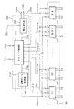
図2は、本発明の実施形態による表示装置の概略的な平面図である。 FIG. 2 is a schematic plan view of a display device according to an embodiment of the present invention.
図2を参照すると、表示装置は表示パネル100及び駆動装置500を含む。
Referring to FIG. 2, the display device includes a
表示パネル100は、下部基板110と上部基板120、及び下部基板110と上部120との間に介在された液晶層(図示せず)を含み、表示領域(DA)と表示領域(DA)を囲む周辺領域(PAで構成される。
The
表示領域(DA)には、複数のソース配線(DL)とソース配線(DL)と交差する複数のゲート配線(GL)が形成される。ソース配線(DL)とゲート配線(GL)によって複数の画素部(P)が定義され、それぞれの画素部(P)には、薄膜トランジスタなどのようなスイッチング素子(TFT)とスイッチング素子(TFT)に電気的に連結された液晶キャパシタ(CLC)及びストレージキャパシタ(CST)が形成される。 In the display area (DA), a plurality of source lines (DL) and a plurality of gate lines (GL) intersecting the source lines (DL) are formed. A plurality of pixel portions (P) are defined by the source wiring (DL) and the gate wiring (GL), and each pixel portion (P) includes a switching element (TFT) such as a thin film transistor and a switching element (TFT). An electrically connected liquid crystal capacitor (CLC) and a storage capacitor (CST) are formed.
駆動装置500は、メイン駆動部200、ソース駆動部300、及びゲート駆動部400を含む。
The
メイン駆動部200は、ソース印刷回路基板201に実装されて表示パネル100を駆動するための駆動信号を出力する。
The
ソース駆動部300は、表示パネル100の周辺領域(PA)に実装されるか、集積されて形成される。ソース駆動部300は、複数のソース駆動チップを有し、各ソース駆動チップは所定個のソース配線(DL)にデータ信号を伝達する。
The
ゲート駆動部400は、表示パネル100の周辺領域(PA)に実装されるか、集積されて形成される。ゲート駆動部400は、複数のゲート駆動チップを有し、各ゲート駆動チップは、所定個のゲート配線(GL)にゲート信号を伝達する。
The
図3は、図2に示したメイン駆動部に対する詳細なブロック図である。 FIG. 3 is a detailed block diagram of the main driving unit shown in FIG.
図2及び図3を参照すると、メイン駆動部200は、タイミング制御部210、電圧発生部230、及び基準ガンマ処理部250を含む。
Referring to FIGS. 2 and 3, the
タイミング制御部210は、外部装置から提供される制御信号202aに基づいて電圧発生部230を制御する第1制御信号210aと、基準ガンマ処理部260を制御する第2制御信号210bと、ソース駆動部300を制御する第3制御信号210c、及びゲート駆動部400を制御する第4制御信号210dを出力する。
The
タイミング制御部210は、外部装置から入力されたデータ信号202bをフレーム単位として処理し、処理されたデータ信号210eをソース駆動部300に出力する。具体的に、タイミング制御部210は、制御信号202aのうち、垂直同期信号(VSYNC)の個数をカウントして現在入力されたデータ信号202bが奇数番目のフレームであるか、偶数番目のフレームか判別する。
The
タイミング制御部210は、データ信号202bが奇数番目のフレームである場合、データ信号202eをソース駆動部300のソース駆動チップ(310、320、330、340)に出力する。一方、データ信号202eが偶数番目のフレームである場合、データ信号202eを1Hの間に遅延させた後、ソース駆動チップ(310、320、330、340)に出力する。
When the
電圧発生部230は、外部から提供された電源電圧202cに基づいて表示装置を駆動するための駆動電圧を発生する。具体的に、駆動電圧は、ソース駆動部300を駆動するためのアナログ駆動電圧(AVDD)230aと、ゲート駆動部400を駆動するためのゲート駆動電圧(VON、VOFF)230b、及び表示パネル100の液晶キャパシタ(CLC)、及びストレージキャパシタ(CST)の共通電圧(VCOM、VST)230cを含む。
The
基準ガンマ処理部250は、第2制御信号210bに基づいて基準ガンマ電圧250aを所定周期に出力する。所定周期は、例えば、17Hである。ここで、所定周期は多様な長さを有することができる。基準ガンマ処理部250は、第2制御信号210bに基づいて既に保存されていた基準ガンマデータを読み出してアナログ形態の基準ガンマ電圧250aに変換して出力する。
The reference
ここで、基準ガンマ電圧250aは、一つの配線を通じてシリアル方式でソース駆動チップ(310、320、330、340)にそれぞれ出力する。前記のようなシリアル方式によると、表示パネル100の周辺領域(PA)に形成される配線の数を減少することができて効果的である。
Here, the
図4は、図3に示したタイミング制御部に対する詳細なブロック図である。 FIG. 4 is a detailed block diagram of the timing control unit shown in FIG.
図3及び図4を参照すると、タイミング制御部210は、制御部211、制御信号生成部212、データ入力部213、保存部214、及びデータ出力部215を含む。
3 and 4, the
制御部211は、タイミング制御部210の全般的な動作を制御する。制御部211は、外部から入力される制御信号202aにおける原始制御信号(CONTL)のうち、垂直同期信号(VSYNC)の個数をカウントして現在入力されるデータ信号が奇数番目または偶数番目のフレームデータであるか判断する。制御部211は、判断結果に基づいてデータ出力部215の出力を制御する。
The
制御信号生成部212は、入力された原始クロック信号(MCLK)と制御信号202aにおける原始制御信号(CONTL)に基づいて第1乃至第4制御信号(210a、210b、210c、210d)を生成して出力する。原始制御信号(CONTL)は、水平同期信号(HSYNC)、垂直同期信号(VSYNC)、データイネーブル信号(DE)を含む。
The
第1制御信号210aは、電圧発生部230を制御する。第2制御信号210bは、所定周期、例えば、17H間隔に基準ガンマ処理部250を制御してリフレッシュされた基準ガンマ電圧250aをソース駆動部300に出力させる。
The
第3制御信号210cは、水平開始信号(STH)、ロード信号(TP)、反転信号(REV)を含む。反転信号(REV)は、2×1反転方式に対応する制御信号である。第4制御信号210dは、垂直開始信号(STV)、第1クロック信号(CK)、第2クロック信号(CKB)を含む。
The
データ入力部213は、外部装置から第1インターフェース方式(例えば、LVDS;Low Voltage Differential Signal)を通じてデータ信号202bが入力される。データ信号202bは、赤色(R)、緑色(G)、及び青色(B)データ信号を含む。
The data input unit 213 receives a
保存部214は、データ入力部213を通じてデータ信号を所定の単位で保存する。望ましくは、保存部214は、データ信号をフレーム単位で保存する。
The
データ出力部215は、制御部211の制御によって保存部214に保存された読み出されたデータ信号210eをソース駆動部300のそれぞれのソース駆動チップ(310、320、330、340)に一対一(point to point)方式で伝送する。
The
データ出力部215は、制御部211の判断結果、奇数番目のフレームに該当する場合、保存部214から読み出されたデータ信号をソース駆動部に出力する。一方、制御部211の判断結果、偶数番目のフレームデータである場合、保存部214から読み出されたデータ信号を1Hの間に遅延させた後、ソース駆動部300に出力する。また、制御部211は、基準ガンマ処理部250を1H区間遅延させた後から駆動させる。
The
したがって、偶数番目のフレームのデータ信号210eは、奇数番目のフレームのデータ信号210eが処理された後、1H区間遅延された後から処理される。
Therefore, the
図5は、図3に示した基準ガンマ処理部に対する詳細なブロック図である。 FIG. 5 is a detailed block diagram of the reference gamma processing unit shown in FIG.
図3及び図5を参照すると、基準ガンマ処理部250は、ガンマ保存部251及びデジタルアナログ変換器253を含む。ガンマ保存部251には、基準ガンマデータが保存される。基準ガンマデータは、全体階調レベルのうち、サンプリングされた所定個(例えば、10〜20個)の階調レベルに該当するガンマ電圧データである。
Referring to FIGS. 3 and 5, the reference
勿論、示していないが、ガンマ保存部251には、赤色(R)、緑色(G)、及び青色(B)それぞれに対応する赤色基準ガンマデータ、緑色基準ガンマデータ、及び青色基準ガンマデータを保存することができる。
Of course, although not shown, the
ガンマ保存部251は、タイミング制御部210の第2制御信号210bに基づいて所定周期に読み出される。ここで、所定周期は17Hを例にする。
The
デジタルアナログ変換器253は、ガンマ保存部251から読み出された基準ガンマデータをアナログ形態の基準ガンマ電圧(250a)に変換してソース駆動部300のそれぞれのソース駆動チップ(310、320、330、340)に連続に伝送される。前記のように、基準ガンマ電圧(250a)がそれぞれのソース駆動チップ(310、320、330、340)に連続に伝送される方式を[シリアルガンマ電圧方式]と称する。
The digital-to-
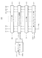
図6は、図3に示したソース駆動チップに対するブロック図である。ここで、多様なソース駆動チップがソース駆動部300上に配置することもできる。
FIG. 6 is a block diagram of the source driving chip shown in FIG. Here, various source driving chips may be disposed on the
図3及び図6を参照すると、それぞれのソース駆動チップ310は、第1サンプル/ホールド部(S/H)311、ラッチ部312、第2サンプル/ホールド部313、デジタルアナログ変換部314、及びバッファ部315を含む。
3 and 6, each
第1サンプル/ホールド部311は、タイミング制御部210から連続に入力される所定個のデータ信号210eを第3制御部210cからの水平開始信号(STH)に基づいてサンプリングしホールディングする。第1サンプル/ホールド部311にサンプリングされた所定個のデータ信号210eは、制御信号(CLK)に基づいてラッチ部312に出力される。
The first sample /
ラッチ部312は、第1サンプル/ホールド部311から出力されたデータ信号を一定時間ラッチさせる。ラッチ部312は、第3制御部210cからのロード信号(TP)が入力されると、ラッチされたデータ信号をデジタルアナログ変換部314に出力する。
The
第2サンプル/ホールド部313は、基準ガンマ処理部250から出力された基準ガンマ電圧250aが連続に入力されると、基準ガンマ電圧250aをサンプリングしホールディングする。基準ガンマ処理部250は、タイミング制御部210の制御によって所定周期(例えば、17H)に入力される。
When the
第2サンプル/ホールド部313は、ホールディングされた基準ガンマ電圧をデジタルアナログ変換部314に出力する。即ち、17H周期にデジタルアナログ変換部314に出力する。
The second sample /
デジタルアナログ変換部314は、第2サンプル/ホールド部313から提供された基準ガンマ電圧を用いてラッチ部312からのデータ信号をアナログ形態のデータ電圧に変換してバッファ部315に出力する。
The digital /
バッファ部315は、アナログ形態のデータ信号を第3制御信号210cにおける反転信号(REV)に基づいてデータ電圧の極性を反転させる。反転信号(REV)は、2×1反転方式によって、2Hを周期としてデータ電圧を反転させる。
The
バッファ部315から出力されたデータ電圧(D1、D2、D3、…DK−2、DK−1、DK)は、表示パネル100に形成されたソース配線(DL)に出力される。
Data voltages (D1, D2, D3,... DK-2, DK-1, DK) output from the
図7は、図6に示したソース駆動チップの入力信号に対するタイミング図である。 FIG. 7 is a timing diagram for an input signal of the source driving chip shown in FIG.
図6及び図7を参照すると、ソース駆動チップ310の入力信号のうち、第3制御信号210cにおけるロード信号(TP)と電圧発生部230からのアナログ駆動電圧(AVDD)に対するタイミング図である。
6 and 7 are timing diagrams with respect to the load signal (TP) in the
ロード信号(TP)は、1Hを周期にソース駆動チップ310に入力され、ラッチ部312にラッチされたデータ信号をデジタルアナログ変換部314に出力させる。究極的にロード信号(TP)は、ラッチ部312を制御して表示パネル100上のソース配線(DL)にデータ電圧をローディングさせる制御信号である。
The load signal (TP) is input to the
電圧発生部230からのアナログ駆動電圧(AVDD)230aは、ソース駆動チップ310に提供され、アナログ駆動のための電源電圧を提供する。
An analog driving voltage (AVDD) 230a from the
ソース駆動チップ310は、2×1反転方式によって2H周期に反転された極性のデータ電圧を出力する。これによって、図示したようにアナログ駆動電圧(AVDD)230aにはリップルが発生する。
The
具体的に、奇数番目の水平区間(OH)には、正常的なレベルのアナログ駆動電圧(例えば、8V)によってソース駆動チップ310が駆動される。反面、偶数番目の水平区間(EH)には、リップルによって正常的なレベルより低いアナログ駆動電圧(例えば、7.8V)によってソース駆動チップ310が駆動するようになる。
Specifically, in the odd-numbered horizontal section (OH), the
第2サンプル/ホールド部313で連続的に入力される基準ガンマ電圧250aを偶数番目の水平区間(EH)にホールディングする場合、基準ガンマ電圧250aにもアナログ駆動電圧(AVDD)230aのリップルが反映されるようになる。
When the
これによって、デジタルアナログ変換部314から出力されるデータ電圧もまた、基準ガンマ電圧250aに基づいて生成されることによってリップルによるエラーが発生する。奇数番目の水平区間(OH)にホールティングされた第1基準ガンマ電圧に対応する第1データ電圧は偶数番目の水平区間(EH)にホールディングされた第2基準ガンマ電圧に対応する第2データ電圧の間に階調差が発生する。
As a result, the data voltage output from the digital-
前記のように、2×1反転方式とシリアルガンマ電圧方式が採用された表示装置においては、基準ガンマ電圧250aがホールディングされる区間によるアナログ駆動電圧の電圧偏差によって横ストライプ形態の暗いストライプ及び明るいストライプが発生する。
As described above, in a display device employing the 2 × 1 inversion method and the serial gamma voltage method, dark stripes and bright stripes in the form of horizontal stripes are generated depending on the voltage deviation of the analog drive voltage depending on the interval in which the
以下、図8乃至図13を参照して横ストライプ形態の画質不良が除去される過程を詳細に説明する。 Hereinafter, a process of removing the image quality defect in the horizontal stripe form will be described in detail with reference to FIGS. 8 to 13.
図8は、図3に示したメイン駆動部の駆動方法を説明するためのフローチャートである。図9は、図3に示したメイン駆動部の入出力信号に対するタイミング図である。図10及び図11は、図9の駆動方式による隣接するフレーム画面の概念図である。 FIG. 8 is a flowchart for explaining a driving method of the main driving unit shown in FIG. FIG. 9 is a timing diagram for input / output signals of the main driving unit shown in FIG. 10 and 11 are conceptual diagrams of adjacent frame screens according to the driving method of FIG.
図3乃至図9を参照すると、電圧発生部230は、ソース駆動部300のソース駆動チップ(310、320、330、340)にアナログ駆動のためのアナログ駆動電圧(AVDD)230aを印加する。
3 to 9, the
ソース駆動チップ(310、320、330、340)は、アナログ駆動電圧(AVDD)を用いてデジタル形態のデータ信号210eをアナログ形態のデータ電圧(D1、…DK)に変換して出力する。図示したように、ソース駆動チップ(310、320、330、340)に印加されるアナログ駆動電圧(AVDD)230aは、2×1反転駆動によるリップルによって2H間隔に電圧変動幅が発生する。 The source driving chips (310, 320, 330, 340) convert the digital data signal 210e into analog data voltages (D1,... DK) using the analog driving voltage (AVDD) and output the converted data signals. As shown in the figure, the analog drive voltage (AVDD) 230a applied to the source drive chip (310, 320, 330, 340) has a voltage fluctuation width at intervals of 2H due to ripple caused by 2 × 1 inversion drive.
アナログ駆動電圧(AVDD)は、奇数番目の水平区間(OH)と偶数番目の水平区間(EH)との間に偏差が発生する。即ち、奇数番目の水平区間(OH)には、比較的に正常的なレベル(例えば、8V)を有し、偶数番目の水平区間(EH)には正常レベルより低いレベル(例えば、7.8V)を有する。 The analog drive voltage (AVDD) has a deviation between the odd-numbered horizontal section (OH) and the even-numbered horizontal section (EH). That is, the odd-numbered horizontal section (OH) has a relatively normal level (for example, 8V), and the even-numbered horizontal section (EH) has a level lower than the normal level (for example, 7.8V). ).
タイミング制御部210には、制御信号202a及びデータ信号202bが入力され、制御信号202aは、垂直同期信号を含む(段階S110)。タイミング制御部210は、外部装置から入力される制御信号202aに基づいて入力されるデータ信号202bを信号処理して出力する。
The
具体的に、制御信号202aのうち、垂直同期信号(VSYNC)をカウンティングして(段階S120)、現在入力されたデータ信号が何番目のフレームに該当するか判断する。
Specifically, a vertical synchronization signal (VSYNC) in the
例えば、現在入力されたデータ信号202bが奇数番目のフレーム(2N−1 FRAME)に該当する場合(段階S130)、タイミング制御部210は、ノーマル駆動方式でソース駆動部300を駆動させる(段階S140)。ソース駆動部300のノーマル駆動方式は下記のようである。
For example, when the currently input data signal 202b corresponds to an odd-numbered frame (2N-1 FRAME) (step S130), the
タイミング制御部210は、入力されたデータ信号210eをソース駆動チップ(310、320、330、340)に一対一に伝送する。また、タイミング制御部210は、基準ガンマ処理部250を制御して所定周期(例えば、17H)にリフレッシュされた基準ガンマ電圧250aをソース駆動チップ(310、320、330、340)に伝送するように制御する。
The
ソース駆動チップ310は、奇数番目の水平区間(OH)、即ち、1番目の水平区間(A)に第2サンプル/ホールド部313でホールディングされた第1基準ガンマ電圧250aを用いて1番目のラインから17番目のラインのデータ信号(1、2、…、17)を処理する。
The
その後、偶数番目の水平区間(EH)、即ち、18番目の水平区間(B)で第2サンプル/ホールド部313からホールディングされた第2基準ガンマ電圧を用いて18番目のラインから34番目のラインのデータ信号(18、19、…、34)を処理する。ここで、第1基準ガンマ電圧は、8Vのアナログ駆動電圧(AVDD)230aに対応し、第2基準ガンマ電圧は、7.8Vのアナログ駆動電圧(AVDD)230aに対応する。
Thereafter, the 34th line from the 18th line using the second reference gamma voltage held from the second sample /
このような方式で、タイミング制御部210は、表示パネル100を駆動させて図10に示したように、奇数番目のフレーム画面(2N−1 FRAME)を表示させる。
In this manner, the
図10を参照すると、第1基準ガンマ電圧を用いて処理された1番目のラインから18番目のラインは、相対的に暗い階調(または明るい階調)が示され、第2基準ガンマ電圧を用いて処理された18番目から34番目のラインは、相対的に明るい階調(または暗い階調)が示される。
一方、タイミング制御部210で判断した結果、現在入力されたデータ信号が偶数番目のフレーム(2N FRAME)に該当する場合、タイミング制御部210は、1H遅延駆動方式でソース駆動部300を駆動させる(段階S150)。1H遅延駆動方式は、下記のようである。
Referring to FIG. 10, the first to eighteenth lines processed using the first reference gamma voltage indicate a relatively dark gradation (or light gradation), and the second reference gamma voltage is expressed as follows. The 18th to 34th lines processed by using a relatively bright gradation (or dark gradation) are shown.
On the other hand, as a result of the determination by the
タイミング制御部210は、入力されたデータ信号を1H遅延させた後(段階S135)、ソース駆動チップ(310、320、330、340)を一対一に伝送する(段階140)。また、タイミング制御部210は、基準ガンマ処理部250を1H遅延させた後(段階S135)、駆動させて所定周期(例えば、17H)にリフレッシュされた基準ガンマ電圧をソース駆動チップ(310、320、330、340)に伝送させる(段階S140)。
The
ノーマル駆動方式と比較するとき、第2基準ガンマ電圧は、1H遅延された2H区間にソース駆動チップ(310、320、330、340)に伝送され、リフレッシュされた第1基準ガンマ電圧は、1H遅延された19H区間にソース駆動チップ(310、320、330、340)に伝送される。 When compared with the normal driving method, the second reference gamma voltage is transmitted to the source driving chip (310, 320, 330, 340) in the 2H period delayed by 1H, and the refreshed first reference gamma voltage is delayed by 1H. Is transmitted to the source driving chip (310, 320, 330, 340) in the 19H section.
ソース駆動チップ310は、偶数番目の水平区間(EH)、即ち、2番目の水平区間(C)に第2サンプル/ホールド部313でホールディングされた第2基準ガンマ電圧を用いて1番目のラインから17番目のラインのデータ信号(1’、2’、…、17’)を処理する。その後、奇数番目の水平区間(OH)、即ち、19番目の水平区間(D)に第2サンプル/ホールド部313でホールディングされた第1基準ガンマ電圧を用いて18番目のラインから34番目のラインのデータ信号(18’、19’、…、34’)を処理する。ここで、第2基準ガンマ電圧は、7.8Vのアナログ駆動電圧(AVDD)に対応し、第1基準ガンマ電圧は8Vのアナログ駆動電圧(AVDD)に対応する。
The
このような方式で、タイミング制御部210は、表示装置を駆動させ、図11に示したように、偶数番目のフレーム画面(2N FRAME)を表示させる。
In this manner, the
図11を参照すると、第2基準ガンマ電圧を用いて処理された1番目のラインから17番目のラインは、相対的に明るい階調(または暗い階調)が示され、第1基準ガンマ電圧を用いて処理された18番目から34番目のラインは、相対的に暗い階調(または明るい階調)が示される。 Referring to FIG. 11, the first to 17th lines processed using the second reference gamma voltage indicate a relatively bright gradation (or dark gradation), and the first reference gamma voltage is expressed as follows. The 18th to 34th lines processed by using a relatively dark gradation (or light gradation) are shown.
図10及び図11を参照すると、奇数番目のフレーム画面(2N−1 FRAME)で発生した横ストライプと偶数番目のフレーム画面(2N FRAME)で発生した横ストライプは相反する階調を有する。例えば、奇数番目のフレーム画面(2N−1 FRAME)の1番目のラインから17番目のラインは相対的に暗い階調を有する反面、偶数番目のフレーム画面(2N FRAME)の1番目のラインから17番目のラインは、相対的に明るい階調を示す。 Referring to FIGS. 10 and 11, the horizontal stripes generated on the odd-numbered frame screen (2N-1 FRAME) and the horizontal stripes generated on the even-numbered frame screen (2N FRAME) have opposite gradations. For example, the 17th line from the 1st line of the odd-numbered frame screen (2N-1 FRAME) has a relatively dark gradation, while the 17th line from the 1st line of the even-numbered frame screen (2N FRAME). The second line shows a relatively bright gradation.
これによって、相反する階調を有する奇数番目のフレーム画面(2N−1 FRAME)のストライプと偶数番目のフレーム画面(2N FRAME)のストライプが相殺され横ストライプ形態の画質不良が改善される。 As a result, the stripes of the odd-numbered frame screen (2N-1 FRAME) and the stripes of the even-numbered frame screen (2N FRAME) having opposite gradations cancel each other, and the image quality defect in the horizontal stripe form is improved.
以上、極端な例として、基準ガンマ電圧のリフレッシュ周期が奇数周期である17Hである場合を説明した。 Above, as an extreme example, riffs les Mesh cycle of the reference gamma voltage has described the case where 17H is odd cycle.
しかし、基準ガンマ電圧のリフレッシュ周期が16Hのように偶数周期である場合にも2×1方式によって奇数番目の水平区間(OH)と偶数番目の水平区間(EH)で発生するアナログ駆動電圧(AVDD)の偏差によって横ストライプ形態の画質不良が発生する恐れがある。 However, generated by the reference gamma voltage riffs les Mesh period of the odd-numbered by 2 × 1 mode even if an even cycle as 16H horizontal section (OH) and even-numbered horizontal section (EH) analog driving voltage Due to the deviation of (AVDD), there is a risk of image quality failure in the form of horizontal stripes.
この場合もまた、奇数番目のフレームのデータ信号と偶数番目のフレームのデータ信号との間に1H遅延差を有するように駆動させることで、横ストライプ形態の画質不良を防止することができる。図8の段階S130にて、前記フレームが偶数番目のフレームであると、段階S140に処理される。しかし、前記フレームが偶数番目のフレームでない場合、段階S135でのように周期が1Hだけ遅延され、再び段階S140に処理される。 Also in this case, the image quality in the horizontal stripe form can be prevented by driving the odd-numbered frame data signal and the even-numbered frame data signal so as to have a 1H delay difference. In step S130 of FIG. 8, if the frame is an even-numbered frame, the process is performed in step S140. However, if the frame is not an even-numbered frame, the period is delayed by 1H as in step S135, and the process is performed again in step S140.
以上では、偶数番目のフレームに対応するデータ信号を1H遅延させて処理することを例にしたが、奇数番目のフレームに対応するデータ信号を1H遅延させて処理することができるのは自明である。 In the above, the data signal corresponding to the even-numbered frame is processed with a delay of 1H. However, it is obvious that the data signal corresponding to the odd-numbered frame can be processed with a delay of 1H. .
図12及び図13は、比較例による隣接するフレーム画面の概念図である。図12及び図13を参照すると、奇数番目のフレーム画面(2N−1 FRAME)と偶数番目のフレーム画面(2N FRAME)とに遅延差がない場合である。 12 and 13 are conceptual diagrams of adjacent frame screens according to a comparative example. Referring to FIGS. 12 and 13, there is a case where there is no delay difference between the odd-numbered frame screen (2N-1 FRAME) and the even-numbered frame screen (2N FRAME).
図示したように、奇数番目のフレーム画面(2N−1 FRAME)に発生した横ストライプ形態のストライプの階調と偶数番目のフレーム画面(2N FRAME)に発生した横ストライプ形態のストライプの階調とが同一になる。このような場合には、フレーム画面で一定の領域は継続明るい階調を示し、他の一定の領域は継続暗い階調を示すようになるので、横ストライプ形態の不良が発生するようになることがわかった。 As shown in the figure, the gray level of the stripe in the horizontal stripe form generated on the odd-numbered frame screen (2N-1 FRAME) and the gray level of the stripe in the horizontal stripe form generated on the even-numbered frame screen (2N FRAME) are shown. Be the same. In such a case, a certain area on the frame screen shows a continuous bright gradation, and the other certain areas show a continuous dark gradation, so that a defective horizontal stripe shape occurs. I understood.
100…表示パネル、
200…メイン駆動部、
210…タイミング制御部、
211…制御部、
212…制御信号生成部、
213…データ入力部、
214…保存部、
215…データ出力部、
230…電圧発生部、
250…基準ガンマ処理部、
251…ガンマ保存部、
253…デジタルアナログ変換器、
300…ソース駆動部、
310…ソース駆動チップ、
311…第1サンプル/ホールド部、
312…ラッチ部、
313…第2サンプル/ホールド部、
314…デジタルアナログ変換部、
315…バッファ部、
400…ゲート駆動部。
100 ... display panel,
200 ... main drive unit,
210 ... timing control unit,
211 ... control unit,
212 ... Control signal generation unit,
213 ... Data input section,
214 ... preservation part,
215: Data output unit,
230 ... Voltage generator,
250: Reference gamma processing unit,
251 ... Gamma storage unit,
253 ... Digital-to-analog converter,
300 ... Source drive unit,
310 ... Source drive chip,
311: First sample / hold section,
312 ... Latch part,
313: Second sample / hold section,
314: Digital / analog converter,
315: Buffer part,
400: a gate driving unit.
Claims (3)
所定周期の水平区間間隔でリフレッシュされたアナログ形態の基準ガンマ電圧を出力する基準ガンマ処理部と、
入力されるデータ信号をサンプリングしてホールティングする第1サンプル/ホールド部、前記所定周期で入力される前記基準ガンマ電圧をサンプリングしてホールディングする第2サンプル/ホールド部、及び前記第2サンプル/ホールド部でホールディングされた基準ガンマ電圧を用いて前記第1サンプル/ホールド部から入力された前記データ信号をアナログ形態のデータ電圧に変換するデジタルアナログ変換部、及び前記デジタルアナログ変換部で変換された前記データ電圧の極性を2水平区間を1周期として反転させて出力するバッファ部、を含み、前記所定周期の間、前記基準ガンマ電圧を用いて前記データ信号をアナログ形態の前記データ電圧に変換して画素部に出力するソース駆動部と、
入力されたデータ信号のフレームを垂直同期信号を基にして奇数番目のフレームか偶数番目のフレームかを判断して、奇数番目のフレームの前記データ信号は遅延させずに前記ソース駆動部に出力する一方偶数番目のフレームの前記データ信号は1水平走査区間の時間だけ遅延させて前記ソース駆動部に出力するか、または偶数番目のフレームの前記データ信号は遅延させずに前記ソース駆動部に出力する一方奇数番目のフレームの前記データ信号は1水平走査区間の時間だけ遅延させて前記ソース駆動部に出力する、タイミング制御部と、
前記ソース駆動部が2水平区間を1周期として前記データ電圧を出力することに伴い、前記2水平区間のうち1番目の水平区間である奇数番目の水平区間で正常電圧、2番目の水平区間である偶数番目の水平区間で前記正常電圧より低い電圧となったアナログ駆動電圧を前記ソース駆動部へ供給する電圧発生部と、
を含み、
前記ソース駆動部は、
前記タイミング制御部から入力された奇数番目のフレームまたは偶数番目のフレームの最初の前記所定区間の間の前記データ信号を、当該奇数番目のフレームまたは偶数番目のフレームが入力されたタイミングと同期して前記2水平区間のうち奇数番目の水平区間で前記第2サンプル/ホールド部によりホールドされて出力された第1基準ガンマ電圧によって前記デジタルアナログ変換部により前記データ電圧に変換し、次の前記所定区間の間の前記データ信号を、前記2水平区間のうち偶数番目の水平区間で前記第2サンプル/ホールド部によりホールドされて出力された前記第1基準ガンマ電圧より低い電圧となった第2基準ガンマ電圧によって前記デジタルアナログ変換部により前記データ電圧に変換することを前記所定区間ごとに行い、
前記タイミング制御部から前記1水平走査区間の時間だけ遅延させて入力された偶数番目のフレームまたは奇数番目のフレームの最初の前記所定区間の間の前記データ信号を、当該遅延させて入力された偶数番目のフレームまたは奇数番目のフレームが入力されたタイミングと同期して前記2水平区間のうち偶数番目の水平区間で前記第2サンプル/ホールド部によりホールドされて出力された第2基準ガンマ電圧によって前記デジタルアナログ変換部により前記データ電圧に変換し、次の前記所定区間の間の前記データ信号を、前記2水平区間のうち奇数番目の水平区間で前記第2サンプル/ホールド部によりホールドされて出力された前記第2基準ガンマ電圧より高い電圧となった第1基準ガンマ電圧によって前記デジタルアナログ変換部により前記データ電圧に変換することを前記所定区間ごとに行うことで、
前記偶数番目のフレーム画面と前記奇数番目のフレーム画面で互いに前記所定区間ごとに階調が異なる表示を行わせるためのデータ電圧を出力することを特徴とする表示装置。 A display panel including a plurality of pixel portions for displaying an image;
A reference gamma processing unit that outputs a reference gamma voltage in an analog form refreshed at a horizontal interval of a predetermined period ;
A first sample / hold unit that samples and holds the input data signal, a second sample / hold unit that samples and holds the reference gamma voltage input at the predetermined period , and the second sample / hold unit digital-to-analog converter for converting the data signal input from the first sample / hold section using the holding criteria gamma voltage to the data voltage of the analog form in parts, and converted the in the digital-analog converter A buffer unit that inverts and outputs the polarity of the data voltage with two horizontal intervals as one cycle, and converts the data signal into the analog data voltage using the reference gamma voltage during the predetermined cycle. A source driving unit for outputting to the pixel unit;
To determine whether odd-numbered frame or an even-numbered frame frames of the input data signal based on the vertical synchronizing signal, the data signal of the odd-numbered frames to the source driver without delay wherein the data signal is the source driving unit without either output to the source driver is delayed and time of one horizontal scanning period, or the data signals of the even-numbered frame delay of the even-numbered frames while output A timing control unit that outputs the data signal of the odd-numbered frame that is output to the source driving unit after being delayed by a time of one horizontal scanning section;
As the source driver outputs the data voltage with two horizontal intervals as one cycle, the normal voltage is applied to the odd horizontal segment, which is the first horizontal segment of the two horizontal segments, and the second horizontal segment is selected. A voltage generator that supplies an analog drive voltage that is lower than the normal voltage in an even-numbered horizontal section to the source driver;
Only including,
The source driver is
The data signal during the first predetermined interval of the odd-numbered frame or even-numbered frame input from the timing control unit is synchronized with the timing when the odd-numbered frame or even-numbered frame is input. The digital analog converter converts the data voltage into the data voltage using the first reference gamma voltage held and output by the second sample / hold unit in the odd-numbered horizontal section of the two horizontal sections. The second reference gamma having a voltage lower than the first reference gamma voltage output by being held by the second sample / hold unit in the even-numbered horizontal section of the two horizontal sections. Conversion to the data voltage by the digital-analog converter according to the voltage is performed for each predetermined interval. ,
The even-numbered frame that has been input from the timing control unit after being delayed by the time of the one horizontal scanning section or the first predetermined section of the odd-numbered frame that is input after the delay. The second reference gamma voltage held and output by the second sample / hold unit in the even-numbered horizontal section of the two horizontal sections in synchronization with the timing at which the first frame or the odd-numbered frame is input. The data voltage is converted into the data voltage by a digital-analog converter, and the data signal during the next predetermined interval is held and output by the second sample / hold unit in the odd-numbered horizontal interval of the two horizontal intervals. The digital-to-analog conversion is performed by a first reference gamma voltage that is higher than the second reference gamma voltage. By performing the conversion to the data voltage to each of the predetermined section by,
A display device that outputs a data voltage for performing display with different gradations for each of the predetermined intervals on the even-numbered frame screen and the odd-numbered frame screen .
基準ガンマデータが保存されたガンマ保存部と、
前記基準ガンマデータをアナログ形態の基準ガンマ電圧に変換して前記ソース駆動部に出力するデジタルアナログ変換器と、を含むことを特徴とする請求項1記載の表示装置。 The reference gamma processing unit is
A gamma storage unit storing reference gamma data;
The display device according to claim 1, further comprising: a digital-analog converter that converts the reference gamma data into a reference gamma voltage in an analog form and outputs the analog gamma voltage to the source driver.
前記奇数番目のフレーム画面と前記偶数番目のフレーム画面のそれぞれにおいて同じ前記所定区間ごとに表示されるストライプの明るさを相殺することを特徴とする請求項1または2記載の表示装置。 A stripe having a first gradation is displayed for each horizontal section of the predetermined section of the odd-numbered frame screen by the output from the source driver , and the first section is displayed for each horizontal section of the predetermined section of the even-numbered frame screen. or appears in the display stripes having a second gradation brighter than the gradation, or by displaying a stripe having a first gray level for each horizontal section of the odd-numbered frame screen the predetermined section of the predetermined even numbered frame screen to display the stripe having a second gradation darker than the first gray level for each horizontal section of the section,
3. The display device according to claim 1 , wherein brightness of stripes displayed for each of the same predetermined sections in each of the odd-numbered frame screen and the even-numbered frame screen is canceled out .
Applications Claiming Priority (2)
| Application Number | Priority Date | Filing Date | Title |
|---|---|---|---|
| KR1020050070989A KR101154341B1 (en) | 2005-08-03 | 2005-08-03 | Display device, method and apparatus for driving the same |
| KR10-2005-0070989 | 2005-08-03 |
Publications (3)
| Publication Number | Publication Date |
|---|---|
| JP2007041590A JP2007041590A (en) | 2007-02-15 |
| JP2007041590A5 JP2007041590A5 (en) | 2009-07-02 |
| JP5305570B2 true JP5305570B2 (en) | 2013-10-02 |
Family
ID=37700142
Family Applications (1)
| Application Number | Title | Priority Date | Filing Date |
|---|---|---|---|
| JP2006205128A Expired - Fee Related JP5305570B2 (en) | 2005-08-03 | 2006-07-27 | Display device |
Country Status (4)
| Country | Link |
|---|---|
| US (1) | US7880706B2 (en) |
| JP (1) | JP5305570B2 (en) |
| KR (1) | KR101154341B1 (en) |
| CN (1) | CN1909053B (en) |
Families Citing this family (7)
| Publication number | Priority date | Publication date | Assignee | Title |
|---|---|---|---|---|
| JP2009015103A (en) * | 2007-07-06 | 2009-01-22 | Nec Electronics Corp | Display controller and its control method |
| KR101410955B1 (en) * | 2007-07-20 | 2014-07-03 | 삼성디스플레이 주식회사 | Display apparatus and method of driving the display apparatus |
| CN102023442A (en) * | 2009-09-18 | 2011-04-20 | 群康科技(深圳)有限公司 | Pixel array and driving method thereof as well as display panel adopting pixel array |
| US9779664B2 (en) | 2014-08-05 | 2017-10-03 | Apple Inc. | Concurrently refreshing multiple areas of a display device using multiple different refresh rates |
| US9653029B2 (en) * | 2014-08-05 | 2017-05-16 | Apple Inc. | Concurrently refreshing multiple areas of a display device using multiple different refresh rates |
| CN105741805B (en) | 2016-04-19 | 2019-03-19 | 深圳市华星光电技术有限公司 | The drive system and driving method of liquid crystal display, liquid crystal display |
| KR102470230B1 (en) * | 2017-10-27 | 2022-11-22 | 엘지디스플레이 주식회사 | Organic light emitting display device |
Family Cites Families (14)
| Publication number | Priority date | Publication date | Assignee | Title |
|---|---|---|---|---|
| JPS6271932A (en) * | 1985-09-25 | 1987-04-02 | Toshiba Corp | Driving method for liquid crystal display device |
| GB9024971D0 (en) * | 1990-11-16 | 1991-01-02 | Rank Cintel Ltd | Continuous-motion line-array telecine |
| TW270198B (en) * | 1994-06-21 | 1996-02-11 | Hitachi Seisakusyo Kk | |
| JP3264248B2 (en) * | 1998-05-22 | 2002-03-11 | 日本電気株式会社 | Active matrix type liquid crystal display |
| JP3897454B2 (en) * | 1998-07-10 | 2007-03-22 | キヤノン株式会社 | Display drive circuit |
| JP2002229519A (en) * | 2001-01-31 | 2002-08-16 | Matsushita Electric Ind Co Ltd | Display device and its driving method |
| KR100767364B1 (en) * | 2001-06-19 | 2007-10-17 | 삼성전자주식회사 | Liquid crystal display device and a driving method thereof |
| KR100777705B1 (en) * | 2001-09-07 | 2007-11-21 | 삼성전자주식회사 | Liquid crystal display device and a driving method thereof |
| KR100825094B1 (en) * | 2001-10-29 | 2008-04-25 | 삼성전자주식회사 | Liquid crystal display device and a driving method thereof |
| CN100426364C (en) * | 2001-11-05 | 2008-10-15 | 三星电子株式会社 | Liquid crystal display and driving device thereof |
| KR100859520B1 (en) * | 2001-11-05 | 2008-09-22 | 삼성전자주식회사 | Liquid crystal display and data driver thereof |
| KR100859467B1 (en) * | 2002-04-08 | 2008-09-23 | 엘지디스플레이 주식회사 | Liquid crystal display and driving method thereof |
| KR100525737B1 (en) * | 2003-09-26 | 2005-11-03 | 엘지전자 주식회사 | Method and Apparatus of Driving Plasma Display Panel |
| JP4201193B2 (en) * | 2004-03-17 | 2008-12-24 | ローム株式会社 | Gamma correction circuit and display device including the same |
-
2005
- 2005-08-03 KR KR1020050070989A patent/KR101154341B1/en not_active IP Right Cessation
-
2006
- 2006-07-27 JP JP2006205128A patent/JP5305570B2/en not_active Expired - Fee Related
- 2006-08-02 CN CN200610108369XA patent/CN1909053B/en not_active Expired - Fee Related
- 2006-08-03 US US11/498,936 patent/US7880706B2/en not_active Expired - Fee Related
Also Published As
| Publication number | Publication date |
|---|---|
| CN1909053A (en) | 2007-02-07 |
| KR101154341B1 (en) | 2012-06-13 |
| CN1909053B (en) | 2010-08-11 |
| JP2007041590A (en) | 2007-02-15 |
| US7880706B2 (en) | 2011-02-01 |
| KR20070016374A (en) | 2007-02-08 |
| US20070030224A1 (en) | 2007-02-08 |
Similar Documents
| Publication | Publication Date | Title |
|---|---|---|
| US8416232B2 (en) | Liquid crystal display capable of reducing number of output channels of data driving circuit and preventing degradation of picture quality | |
| JP4988692B2 (en) | Liquid crystal display device and driving method thereof | |
| US7259739B2 (en) | Method and apparatus for driving liquid crystal display | |
| US8031153B2 (en) | Liquid crystal display and driving method thereof | |
| JP4856052B2 (en) | Liquid crystal display device and driving method thereof | |
| JP4989621B2 (en) | Liquid crystal display device and driving method thereof | |
| JP5305570B2 (en) | Display device | |
| JP2005258447A (en) | Liquid crystal panel driving device and its driving method | |
| KR101494451B1 (en) | Display and driving method sameof | |
| KR101924417B1 (en) | Method of driving a display panel and display apparatus for performing the same | |
| JP2007248639A (en) | Liquid crystal driving method and liquid crystal driving device | |
| KR20100041522A (en) | Data driving apparatus, display comprising the same | |
| JP2011065153A (en) | Pixel array and driving method of the same, and display panel having the pixel array | |
| JP2007226226A (en) | Source driving apparatus, method of driving same, display device having same and method of driving same | |
| KR20160084547A (en) | Curved liquid crystal display | |
| KR20060116443A (en) | Display device, apparatus and method for driving thereof | |
| US10621937B2 (en) | Liquid crystal display device and method of driving the same | |
| JP5081456B2 (en) | Display device | |
| KR20080062934A (en) | Dim improvement circuit of liquid crystal display device | |
| JP2014228575A (en) | Liquid crystal display device | |
| KR101282223B1 (en) | Driving apparatus and method for liquid crystal display | |
| JP2010160350A (en) | Liquid crystal display device and method for driving the same | |
| KR101288836B1 (en) | Greenish effect improvement apparatus for liquid crystal display | |
| KR20060135105A (en) | Display device and driving method thereof | |
| JP2007086683A (en) | Liquid crystal display device |
Legal Events
| Date | Code | Title | Description |
|---|---|---|---|
| A521 | Written amendment |
Free format text: JAPANESE INTERMEDIATE CODE: A523 Effective date: 20090518 |
|
| A621 | Written request for application examination |
Free format text: JAPANESE INTERMEDIATE CODE: A621 Effective date: 20090518 |
|
| A521 | Written amendment |
Free format text: JAPANESE INTERMEDIATE CODE: A523 Effective date: 20100419 |
|
| A131 | Notification of reasons for refusal |
Free format text: JAPANESE INTERMEDIATE CODE: A131 Effective date: 20110920 |
|
| A131 | Notification of reasons for refusal |
Free format text: JAPANESE INTERMEDIATE CODE: A131 Effective date: 20120911 |
|
| A521 | Written amendment |
Free format text: JAPANESE INTERMEDIATE CODE: A523 Effective date: 20121129 |
|
| A711 | Notification of change in applicant |
Free format text: JAPANESE INTERMEDIATE CODE: A712 Effective date: 20121213 |
|
| TRDD | Decision of grant or rejection written | ||
| A01 | Written decision to grant a patent or to grant a registration (utility model) |
Free format text: JAPANESE INTERMEDIATE CODE: A01 Effective date: 20130528 |
|
| A61 | First payment of annual fees (during grant procedure) |
Free format text: JAPANESE INTERMEDIATE CODE: A61 Effective date: 20130625 |
|
| R150 | Certificate of patent or registration of utility model |
Free format text: JAPANESE INTERMEDIATE CODE: R150 |
|
| R250 | Receipt of annual fees |
Free format text: JAPANESE INTERMEDIATE CODE: R250 |
|
| R250 | Receipt of annual fees |
Free format text: JAPANESE INTERMEDIATE CODE: R250 |
|
| LAPS | Cancellation because of no payment of annual fees |