JP5286865B2 - Electroluminescent panel manufacturing method and electroluminescent panel - Google Patents
Electroluminescent panel manufacturing method and electroluminescent panel Download PDFInfo
- Publication number
- JP5286865B2 JP5286865B2 JP2008075871A JP2008075871A JP5286865B2 JP 5286865 B2 JP5286865 B2 JP 5286865B2 JP 2008075871 A JP2008075871 A JP 2008075871A JP 2008075871 A JP2008075871 A JP 2008075871A JP 5286865 B2 JP5286865 B2 JP 5286865B2
- Authority
- JP
- Japan
- Prior art keywords
- electrode
- layer
- insulating film
- light
- light shielding
- Prior art date
- Legal status (The legal status is an assumption and is not a legal conclusion. Google has not performed a legal analysis and makes no representation as to the accuracy of the status listed.)
- Expired - Fee Related
Links
- 238000004519 manufacturing process Methods 0.000 title claims description 24
- 230000001681 protective effect Effects 0.000 claims description 32
- 239000000758 substrate Substances 0.000 claims description 29
- 150000002894 organic compounds Chemical class 0.000 claims description 27
- 239000004065 semiconductor Substances 0.000 claims description 20
- 238000005192 partition Methods 0.000 claims description 18
- 239000000463 material Substances 0.000 claims description 17
- 229920005989 resin Polymers 0.000 claims description 16
- 239000011347 resin Substances 0.000 claims description 16
- 238000005401 electroluminescence Methods 0.000 claims description 14
- 229910052751 metal Inorganic materials 0.000 claims description 14
- 239000002184 metal Substances 0.000 claims description 14
- 239000000049 pigment Substances 0.000 claims description 5
- 239000010410 layer Substances 0.000 description 120
- 239000010408 film Substances 0.000 description 58
- 238000002347 injection Methods 0.000 description 24
- 239000007924 injection Substances 0.000 description 24
- 238000000034 method Methods 0.000 description 16
- 239000007788 liquid Substances 0.000 description 12
- 230000004048 modification Effects 0.000 description 9
- 238000012986 modification Methods 0.000 description 9
- 239000003990 capacitor Substances 0.000 description 8
- 238000007789 sealing Methods 0.000 description 7
- 238000000576 coating method Methods 0.000 description 5
- 238000007740 vapor deposition Methods 0.000 description 5
- VYPSYNLAJGMNEJ-UHFFFAOYSA-N Silicium dioxide Chemical compound O=[Si]=O VYPSYNLAJGMNEJ-UHFFFAOYSA-N 0.000 description 4
- 239000011159 matrix material Substances 0.000 description 4
- 229920001609 Poly(3,4-ethylenedioxythiophene) Polymers 0.000 description 3
- XUIMIQQOPSSXEZ-UHFFFAOYSA-N Silicon Chemical compound [Si] XUIMIQQOPSSXEZ-UHFFFAOYSA-N 0.000 description 3
- RTAQQCXQSZGOHL-UHFFFAOYSA-N Titanium Chemical compound [Ti] RTAQQCXQSZGOHL-UHFFFAOYSA-N 0.000 description 3
- 239000006229 carbon black Substances 0.000 description 3
- 229920000547 conjugated polymer Polymers 0.000 description 3
- 239000012535 impurity Substances 0.000 description 3
- 229910003437 indium oxide Inorganic materials 0.000 description 3
- PJXISJQVUVHSOJ-UHFFFAOYSA-N indium(iii) oxide Chemical compound [O-2].[O-2].[O-2].[In+3].[In+3] PJXISJQVUVHSOJ-UHFFFAOYSA-N 0.000 description 3
- 238000000059 patterning Methods 0.000 description 3
- 229910052710 silicon Inorganic materials 0.000 description 3
- 239000010703 silicon Substances 0.000 description 3
- 239000002904 solvent Substances 0.000 description 3
- CXWXQJXEFPUFDZ-UHFFFAOYSA-N tetralin Chemical compound C1=CC=C2CCCCC2=C1 CXWXQJXEFPUFDZ-UHFFFAOYSA-N 0.000 description 3
- 239000010936 titanium Substances 0.000 description 3
- 229910052719 titanium Inorganic materials 0.000 description 3
- 239000004925 Acrylic resin Substances 0.000 description 2
- 229920000178 Acrylic resin Polymers 0.000 description 2
- 239000004642 Polyimide Substances 0.000 description 2
- 229910052581 Si3N4 Inorganic materials 0.000 description 2
- 229910021417 amorphous silicon Inorganic materials 0.000 description 2
- 229910052788 barium Inorganic materials 0.000 description 2
- 229910052791 calcium Inorganic materials 0.000 description 2
- 239000011575 calcium Substances 0.000 description 2
- 239000011651 chromium Substances 0.000 description 2
- 229920001940 conductive polymer Polymers 0.000 description 2
- 238000010586 diagram Methods 0.000 description 2
- 239000002019 doping agent Substances 0.000 description 2
- 239000003822 epoxy resin Substances 0.000 description 2
- 230000002209 hydrophobic effect Effects 0.000 description 2
- 229920000647 polyepoxide Polymers 0.000 description 2
- 229920001721 polyimide Polymers 0.000 description 2
- UOHMMEJUHBCKEE-UHFFFAOYSA-N prehnitene Chemical compound CC1=CC=C(C)C(C)=C1C UOHMMEJUHBCKEE-UHFFFAOYSA-N 0.000 description 2
- 239000013557 residual solvent Substances 0.000 description 2
- HQVNEWCFYHHQES-UHFFFAOYSA-N silicon nitride Chemical compound N12[Si]34N5[Si]62N3[Si]51N64 HQVNEWCFYHHQES-UHFFFAOYSA-N 0.000 description 2
- 229910052814 silicon oxide Inorganic materials 0.000 description 2
- 229920005992 thermoplastic resin Polymers 0.000 description 2
- 229920001187 thermosetting polymer Polymers 0.000 description 2
- 239000010409 thin film Substances 0.000 description 2
- 229910001316 Ag alloy Inorganic materials 0.000 description 1
- IJGRMHOSHXDMSA-UHFFFAOYSA-N Atomic nitrogen Chemical compound N#N IJGRMHOSHXDMSA-UHFFFAOYSA-N 0.000 description 1
- OYPRJOBELJOOCE-UHFFFAOYSA-N Calcium Chemical compound [Ca] OYPRJOBELJOOCE-UHFFFAOYSA-N 0.000 description 1
- VYZAMTAEIAYCRO-UHFFFAOYSA-N Chromium Chemical compound [Cr] VYZAMTAEIAYCRO-UHFFFAOYSA-N 0.000 description 1
- WHXSMMKQMYFTQS-UHFFFAOYSA-N Lithium Chemical compound [Li] WHXSMMKQMYFTQS-UHFFFAOYSA-N 0.000 description 1
- FYYHWMGAXLPEAU-UHFFFAOYSA-N Magnesium Chemical compound [Mg] FYYHWMGAXLPEAU-UHFFFAOYSA-N 0.000 description 1
- CBENFWSGALASAD-UHFFFAOYSA-N Ozone Chemical compound [O-][O+]=O CBENFWSGALASAD-UHFFFAOYSA-N 0.000 description 1
- BQCADISMDOOEFD-UHFFFAOYSA-N Silver Chemical compound [Ag] BQCADISMDOOEFD-UHFFFAOYSA-N 0.000 description 1
- 229910006404 SnO 2 Inorganic materials 0.000 description 1
- WGLPBDUCMAPZCE-UHFFFAOYSA-N Trioxochromium Chemical compound O=[Cr](=O)=O WGLPBDUCMAPZCE-UHFFFAOYSA-N 0.000 description 1
- XLOMVQKBTHCTTD-UHFFFAOYSA-N Zinc monoxide Chemical compound [Zn]=O XLOMVQKBTHCTTD-UHFFFAOYSA-N 0.000 description 1
- 229910045601 alloy Inorganic materials 0.000 description 1
- 239000000956 alloy Substances 0.000 description 1
- 229910052782 aluminium Inorganic materials 0.000 description 1
- XAGFODPZIPBFFR-UHFFFAOYSA-N aluminium Chemical compound [Al] XAGFODPZIPBFFR-UHFFFAOYSA-N 0.000 description 1
- QVGXLLKOCUKJST-UHFFFAOYSA-N atomic oxygen Chemical compound [O] QVGXLLKOCUKJST-UHFFFAOYSA-N 0.000 description 1
- DSAJWYNOEDNPEQ-UHFFFAOYSA-N barium atom Chemical compound [Ba] DSAJWYNOEDNPEQ-UHFFFAOYSA-N 0.000 description 1
- BEQNOZDXPONEMR-UHFFFAOYSA-N cadmium;oxotin Chemical compound [Cd].[Sn]=O BEQNOZDXPONEMR-UHFFFAOYSA-N 0.000 description 1
- 230000015556 catabolic process Effects 0.000 description 1
- 229910052804 chromium Inorganic materials 0.000 description 1
- 229910000423 chromium oxide Inorganic materials 0.000 description 1
- 239000011248 coating agent Substances 0.000 description 1
- 239000003086 colorant Substances 0.000 description 1
- 239000004020 conductor Substances 0.000 description 1
- 238000006731 degradation reaction Methods 0.000 description 1
- 238000000151 deposition Methods 0.000 description 1
- 229910001873 dinitrogen Inorganic materials 0.000 description 1
- 238000003618 dip coating Methods 0.000 description 1
- 230000000694 effects Effects 0.000 description 1
- 238000005530 etching Methods 0.000 description 1
- 239000000945 filler Substances 0.000 description 1
- 229910052738 indium Inorganic materials 0.000 description 1
- APFVFJFRJDLVQX-UHFFFAOYSA-N indium atom Chemical compound [In] APFVFJFRJDLVQX-UHFFFAOYSA-N 0.000 description 1
- 239000011261 inert gas Substances 0.000 description 1
- 239000011229 interlayer Substances 0.000 description 1
- 150000002500 ions Chemical class 0.000 description 1
- 238000010030 laminating Methods 0.000 description 1
- 229910052744 lithium Inorganic materials 0.000 description 1
- 229910052749 magnesium Inorganic materials 0.000 description 1
- 239000011777 magnesium Substances 0.000 description 1
- AUHZEENZYGFFBQ-UHFFFAOYSA-N mesitylene Substances CC1=CC(C)=CC(C)=C1 AUHZEENZYGFFBQ-UHFFFAOYSA-N 0.000 description 1
- 125000001827 mesitylenyl group Chemical group [H]C1=C(C(*)=C(C([H])=C1C([H])([H])[H])C([H])([H])[H])C([H])([H])[H] 0.000 description 1
- 239000000203 mixture Substances 0.000 description 1
- 239000003960 organic solvent Substances 0.000 description 1
- 239000001301 oxygen Substances 0.000 description 1
- 229910052760 oxygen Inorganic materials 0.000 description 1
- SWELZOZIOHGSPA-UHFFFAOYSA-N palladium silver Chemical compound [Pd].[Ag] SWELZOZIOHGSPA-UHFFFAOYSA-N 0.000 description 1
- 238000000206 photolithography Methods 0.000 description 1
- 238000005240 physical vapour deposition Methods 0.000 description 1
- 238000009832 plasma treatment Methods 0.000 description 1
- 229920000553 poly(phenylenevinylene) Polymers 0.000 description 1
- 229910021420 polycrystalline silicon Inorganic materials 0.000 description 1
- 229920002098 polyfluorene Polymers 0.000 description 1
- -1 polyphenylene vinylene Polymers 0.000 description 1
- 229920005591 polysilicon Polymers 0.000 description 1
- 229910052761 rare earth metal Inorganic materials 0.000 description 1
- 150000002910 rare earth metals Chemical class 0.000 description 1
- 238000005215 recombination Methods 0.000 description 1
- 230000006798 recombination Effects 0.000 description 1
- 239000000377 silicon dioxide Substances 0.000 description 1
- 229910052709 silver Inorganic materials 0.000 description 1
- 239000004332 silver Substances 0.000 description 1
- 238000004528 spin coating Methods 0.000 description 1
- 239000000126 substance Substances 0.000 description 1
- XOLBLPGZBRYERU-UHFFFAOYSA-N tin dioxide Chemical compound O=[Sn]=O XOLBLPGZBRYERU-UHFFFAOYSA-N 0.000 description 1
- 229910001887 tin oxide Inorganic materials 0.000 description 1
- 238000001771 vacuum deposition Methods 0.000 description 1
- XLYOFNOQVPJJNP-UHFFFAOYSA-N water Substances O XLYOFNOQVPJJNP-UHFFFAOYSA-N 0.000 description 1
Images


Description
本発明は、エレクトロルミネッセンスパネルの製造方法及びエレクトロルミネッセンスパネルに関する。 The present invention relates to a method for manufacturing an electroluminescence panel and an electroluminescence panel.
有機エレクトロルミネッセンス素子はアノードとカソードとの間に有機化合物層が介在した積層構造を為しており、アノードとカソードの間に順バイアス電圧が印加されると、有機化合物層内で電子と正孔が再結合引き起こして有機化合物層が発光する。それぞれ赤、緑、青に発光する複数の有機エレクトロルミネッセンス素子をサブピクセルとして基板上にマトリクス状に配列し、画像表示を行うエレクトロルミネッセンスディスプレイパネルが実現化されている。 An organic electroluminescent element has a laminated structure in which an organic compound layer is interposed between an anode and a cathode. When a forward bias voltage is applied between the anode and the cathode, electrons and holes are formed in the organic compound layer. Cause recombination and the organic compound layer emits light. An electroluminescence display panel that displays images by arranging a plurality of organic electroluminescence elements that emit red, green, and blue as subpixels in a matrix on a substrate has been realized.
アクティブ駆動の場合、画素トランジスタを基板上に形成した後、画素トランジスタを覆う保護絶縁膜を形成し、保護絶縁膜の上に画素電極を形成した後に画素電極上に有機化合物層を形成する構造が知られている(例えば、特許文献1参照)。
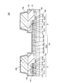
ところで、図17に示すように、製造プロセスの簡略化のために、基板上に画素トランジスタ121と画素電極120aとを形成し、画素トランジスタ121及び画素電極120aを覆う保護絶縁膜132に画素電極120aを露出させる露出孔133を形成し、画素電極120a上に有機化合物層120bを形成する構造が検討されている。
Incidentally, as shown in FIG. 17, in order to simplify the manufacturing process, the pixel transistor 121 and the
しかし、保護絶縁膜132は光を透過させるため、この構造では、図17に示すように、有機化合物層120bから側方に放出される光や絶縁基板102で反射した光が保護絶縁膜132に入射し、隔壁106を通過して対向電極120dで反射されて画素トランジスタ121に到達することが考えられる。このような場合、画素トランジスタ121に光劣化を引き起こすなどの不都合が考えられる。
However, since the protective
本発明の課題は、有機エレクトロルミネッセンス素子から放射される光により画素トランジスタが劣化することを防止することである。 An object of the present invention is to prevent a pixel transistor from being deteriorated by light emitted from an organic electroluminescence element.
請求項1に記載の発明は、エレクトロルミネッセンスパネルにおいて、
透明な基板と、
前記基板の一面上に設けられた画素電極と、
前記基板の前記一面上に、同じ金属層により同じ層に形成されたゲート電極及び該ゲート電極と離間して形成された第1遮光層と、前記基板の前記一面上に形成されて前記ゲート電極を覆うゲート絶縁膜と、前記ゲート絶縁膜の上部に形成された半導体膜と、を有して、前記画素電極に接続され、前記第1遮光層が少なくとも前記半導体膜に対向する位置に設けられた画素トランジスタと、
前記画素電極の上部に形成された、発光層を含む有機化合物層と、
前記有機化合物層の上部に形成された対向電極と、
前記画素トランジスタを覆う保護絶縁膜と、
前記保護絶縁膜上の前記画素トランジスタに対応する領域に設けられた第2遮光層と、
前記保護絶縁膜及び前記第2遮光層の上部に設けられた隔壁と、
を備え、
前記第2遮光膜は、該遮光膜の前記画素トランジスタ側の面に入射する前記発光層から放射される光の一部を吸収する材料を含んでいることを特徴とする。
The invention according to claim 1 is an electroluminescence panel,
A transparent substrate,
A pixel electrode provided on one surface of the substrate;
A gate electrode formed in the same layer by the same metal layer on the one surface of the substrate; a first light-shielding layer formed away from the gate electrode; and the gate electrode formed on the one surface of the substrate. A gate insulating film that covers the gate insulating film and a semiconductor film formed on the gate insulating film, and is connected to the pixel electrode, and the first light shielding layer is provided at least at a position facing the semiconductor film. A pixel transistor,
An organic compound layer including a light emitting layer formed on the pixel electrode;
A counter electrode formed on the organic compound layer;
A protective insulating film covering the pixel transistor;
A second light shielding layer provided in a region corresponding to the pixel transistor on the protective insulating film;
A partition wall provided on the protective insulating film and the second light shielding layer;
With
The second light shielding film includes a material that absorbs part of light emitted from the light emitting layer incident on a surface of the light shielding film on the pixel transistor side.
前記画素トランジスタは半導体膜、ゲート電極、ソース電極及びドレイン電極を有し、前記ソース電極及び前記ドレイン電極が配列する方向における前記半導体膜の幅が前記ゲート電極の幅よりも長く、前記ソース電極及び前記ドレイン電極が配列する方向における前記遮光層の幅が前記ゲート電極の幅よりも長いことを特徴とする。The pixel transistor includes a semiconductor film, a gate electrode, a source electrode, and a drain electrode, and a width of the semiconductor film in a direction in which the source electrode and the drain electrode are arranged is longer than a width of the gate electrode, The width of the light shielding layer in the direction in which the drain electrodes are arranged is longer than the width of the gate electrode.
前記遮光層は黒色顔料を分散させた樹脂材料を含んでいてもよい。 The light shielding layer may include a resin material in which a black pigment is dispersed .
前記遮光層は絶縁性であってもよい。The light shielding layer may be insulative.
請求項5に記載の発明は、エレクトロルミネッセンスパネルの製造方法において、
画素電極と、対向電極と、前記画素電極と前記対向電極との間に介在する発光層を含む有機化合物層と、前記画素電極に接続された画素トランジスタと、を有する基板を備えたエレクトロルミネッセンスパネルの製造方法であって、
前記基板の一面上に、同じ金属層により同じ層に、前記画素トランジスタのゲート電極及び該ゲート電極と離間した第1遮光層を形成し、
前記基板の前記一面上に、前記ゲート電極を覆う前記画素トランジスタのゲート絶縁膜を形成し、
前記ゲート絶縁膜の上部に前記画素トランジスタの半導体膜を形成し、
前記基板の前記一面上に、前記画素トランジスタを覆う保護絶縁膜を形成し、
前記保護絶縁膜上の前記画素トランジスタに対応する領域に、前記画素トランジスタ側の面に前記発光層から放射される光の一部が入射するように第2遮光層を形成し、
前記保護絶縁膜及び前記第2遮光層の上部に隔壁を形成し、
前記第1遮光層を、少なくとも前記半導体膜に対向する位置に形成し、
前記第2遮光膜を、前記入射する光を吸収する材料により形成することを特徴とする。
Invention of Claim 5 is in the manufacturing method of an electroluminescent panel,
An electroluminescence panel comprising a substrate having a pixel electrode, a counter electrode, an organic compound layer including a light emitting layer interposed between the pixel electrode and the counter electrode, and a pixel transistor connected to the pixel electrode A manufacturing method of
A gate electrode of the pixel transistor and a first light shielding layer spaced from the gate electrode are formed on the same surface of the substrate by the same metal layer,
Forming a gate insulating film of the pixel transistor covering the gate electrode on the one surface of the substrate;
Forming a semiconductor film of the pixel transistor on the gate insulating film;
Forming a protective insulating film covering the pixel transistor on the one surface of the substrate;
Forming a second light-shielding layer so that a part of the light emitted from the light-emitting layer is incident on the surface on the pixel transistor side in a region corresponding to the pixel transistor on the protective insulating film;
Forming partition walls on the protective insulating film and the second light shielding layer;
Forming the first light shielding layer at a position facing at least the semiconductor film;
The second light shielding film is formed of a material that absorbs the incident light.
本発明によれば、有機エレクトロルミネッセンス素子から放射される光により画素トランジスタが劣化することを防止することができる。 ADVANTAGE OF THE INVENTION According to this invention, it can prevent that a pixel transistor deteriorates with the light radiated | emitted from an organic electroluminescent element.
以下に、本発明を実施するための最良の形態について図面を用いて説明する。但し、以下に述べる実施形態には、本発明を実施するために技術的に好ましい種々の限定が付されているが、発明の範囲を以下の実施形態及び図示例に限定するものではない。また、以下の説明において、エレクトロルミネッセンス(Electro Luminescence)という用語をELと略称する。 The best mode for carrying out the present invention will be described below with reference to the drawings. However, although various technically preferable limitations for implementing the present invention are given to the embodiments described below, the scope of the invention is not limited to the following embodiments and illustrated examples. Further, in the following description, the term electroluminescence is abbreviated as EL.
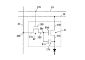
図1は、本発明の実施形態に係るELディスプレイパネル10における1つのサブピクセルの回路図であり、図2は1つのサブピクセルの平面図であり、図3は図2のIII−III矢視断面図である。このELディスプレイパネル10においては、赤、青及び緑のサブピクセルによって1ドットの画素が構成され、このような画素がマトリクス状に配列されている。水平方向の配列に着目すると赤のサブピクセル、青のサブピクセル、緑のサブピクセルの順に繰り返し配列され、垂直方向の配列に着目すると同じ色が一列に配列されている。
1 is a circuit diagram of one subpixel in an
このELディスプレイパネル10においては、サブピクセルに各種の信号を出力するために、複数の走査線25、信号線24及び供給線26が設けられている。走査線25及び供給線26と、信号線24とは互いに直行する方向に延在している。
In the
サブピクセルは、2つのnチャネル型トランジスタ21,22と、キャパシタ27と、有機EL素子20とを有する。2つのnチャネル型トランジスタ21,22及びキャパシタ27は、走査線25、信号線24及び供給線26の入力信号に応じて有機EL素子20に電圧を印加する。
The subpixel includes two n-
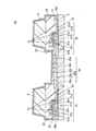
図2、図3に示すように、透明な絶縁基板2の上にトランジスタ21,22のゲート電極21G,22Gが設けられるとともに、キャパシタ27の一方の電極27a、信号線24が設けられ、これらが共通のゲート絶縁膜31によって被覆されている。なお、図2に示すように、電極27aとゲート電極21とは一体に形成されている。
As shown in FIGS. 2 and 3,
ゲート絶縁膜31の上には、図3に示すように、トランジスタ21,22の半導体膜21a,22a、チャネル保護膜21b,22b、不純物半導体膜21c,21d,22c,22d、ソース電極21S,22S及びドレイン電極21D,22D、走査線25及び供給線26が設けられている。なお、図2に示すように、ドレイン電極21Dは供給線26と一体に形成されており、ソース電極22Sはコンタクトホール28aによりゲート電極21G及び電極27aと導通されており、信号線24はコンタクトホール28bによりドレイン電極22Dと導通されており、走査線25はコンタクトホール28cによりゲート電極22と導通されている。
On the
また、ゲート絶縁膜31の上には、サブピクセル電極20a(画素電極)及びキャパシタ27の他方の電極27bがマトリクス状に配列されている。なお、図2に示すように、サブピクセル電極20aと電極27bとは一体に形成されている。
これらサブピクセル電極20a及び電極27bは、気相成長法によってゲート絶縁膜31上に成膜された導電性膜(例えば、錫ドープ酸化インジウム(ITO)、亜鉛ドープ酸化インジウム、酸化インジウム(In2O3)、酸化スズ(SnO2)、酸化亜鉛(ZnO)又はカドミウム−錫酸化物(CTO))をフォトリソグラフィー法及びエッチング法を用いてパターニングすることによって形成されたものである。サブピクセル電極20aはトランジスタ21のソース電極21Sの一部と重なるように形成され、ソース電極21Sと導通している。
On the
The
トランジスタ21,22のソース電極21S,22S及びドレイン電極21D,22D、キャパシタ27の他方の電極27b、走査線25及び供給線26、サブピクセル電極20aは共通の保護絶縁膜32によって被覆されている。保護絶縁膜32のサブピクセル電極20aの部分にはサブピクセル電極20aを露出させる露出孔33が形成されている。露出孔33が形成されることにより保護絶縁膜32はサブピクセル電極20aの間を縫うように網目状に形成されるとともにサブピクセル電極20aの一部外縁部に重なり、サブピクセル電極20aを囲繞している。露出孔33内に後述する有機EL層20bが形成される。
なお、絶縁基板2から保護絶縁膜32までの積層構造がトランジスタアレイパネル50である。
The
The stacked structure from the insulating
保護絶縁膜32上には、図2、図3に示すように、トランジスタ21,22と対応する位置に、有機EL素子20から放出される光を反射しない遮光層8が設けられている。遮光層8としては、有機EL素子20から放出される光を吸収する材料を用いることができ、例えば、TFT−LCDでブラックマトリックス(BM)として汎用されている樹脂BMを使用することができる。汎用型樹脂BMの多くはネガ型の感光性樹脂の中にカーボンブラックやチタンブラックなどの黒色顔料を分散させたものである。
As shown in FIGS. 2 and 3, the
あるいは、遮光層8として、有機EL素子20から放射される光を反射する反射膜を設けてもよい。反射膜としては、例えば酸化クロムIII(Cr2O3)等の金属をPVD等により成膜した金属薄膜等を用いることができる。
Alternatively, as the
また、保護絶縁膜32及び遮光層8の上部には、トランジスタ21,22及び信号線24と対応する位置に、隔壁6が形成されている。隔壁6は、例えばポリイミド等の樹脂により形成されたものであり、トランジスタ21,22の各電極、走査線25、信号線24、供給線26よりも十分に厚い。
A
サブピクセル電極20a上には正孔注入層20e、発光層20fが順に積層されて有機EL層20b(有機化合物層)が形成されている。正孔注入層20eは、導電性高分子であるPEDOT及びドーパントであるPSSからなり、発光層20fは、ポリフェニレンビニレン系発光材料やポリフルオレン系発光材料等の共役ポリマーからなる。なお、有機EL層20bは発光層の上にさらに電子輸送層を設けても良い。また、有機EL層20bはサブピクセル電極20aの上に形成された発光層、電子輸送層からなる二層構造であっても良いし、担体輸送層と発光層との組合せは任意に設定できる。また、これらの層構造において適切な層間に担体輸送を制限するインタレイヤ層が介在した積層構造であっても良いし、その他の積層構造であっても良い。
On the
正孔注入層20e及び発光層20fは、湿式塗布法(例えば、インクジェット法)によって成膜される。この場合、正孔注入層20eとなるPEDOT及びPSSを含有する有機化合物含有液をサブピクセル電極20aに塗布して成膜し、その後、発光層20fとなる共役ポリマー発光材料を含有する有機化合物含有液を塗布して成膜するが、厚膜の隔壁6が設けられているので、隣り合うサブピクセル電極20aに塗布された有機化合物含有液が隔壁6を越えて混ざり合うことを防止することができる。
The
なお、サブピクセルが赤の場合には発光層20fが赤色に発光し、サブピクセルが緑の場合には発光層20fが緑色に発光し、サブピクセルが青の場合には発光層20fが青色に発光するように、それぞれの材料を設定する。
The
発光層20f上には、有機EL素子20のカソードを構成する電子注入層20cが成膜されている。電子注入層20cは、全てのサブピクセルに共通して形成される共通電極である。電子注入層20cは、サブピクセル電極20aよりも仕事関数の低い材料で形成されており、例えば、インジウム、マグネシウム、カルシウム、リチウム、バリウム、希土類金属の少なくとも一種を含む単体又は合金より1〜10nmの厚さに形成されている。あるいは、電子注入層20cは、上記各種材料の層が積層された積層構造となっていても良い。
On the
電子注入層20c、隔壁6及び遮光層8の上部には、例えばアルミニウム、クロム、銀やパラジウム銀系の合金等の導電性材料を気相成長法によって100nm以上成膜することによって対向電極20dが形成されている。
サブピクセル電極20a、有機EL層20b、電子注入層20c、対向電極20dの順に積層されたものが有機EL素子20である。
A
The
なお、図示しないが、対向電極20dの上には、封止層が堆積されており、封止層は表示部3全体を被覆するように形成されている。つまり、封止層は、複数の有機EL素子10全体を被覆するように形成されている。封止層は、絶縁性を有し、例えば、エポキシ樹脂、アクリル樹脂等の熱硬化性樹脂、熱可塑性樹脂又は光硬化性樹脂等からなり、これらの樹脂にシリカ充填材等を加えたものでもよい。封止層は有機EL素子20が外気に露出されることを防ぐ役割を果たす。
Although not shown, a sealing layer is deposited on the
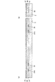
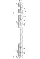
次に、ELディスプレイパネル10を製造する製造工程について説明する。まず、図4〜図13を用いてトランジスタアレイパネル50の製造工程について説明する。なお、図4〜図13において、(a)は図3と同じ断面の図であり、(b)はコンタクトホール28aにおける断面図である。
Next, a manufacturing process for manufacturing the
まず、図4に示すように、絶縁基板2の上部にべた一面にゲート金属35を成膜し、パターニングすることで、ゲート21G,22G及び電極27a、信号線24を形成する。次に、図5に示すように、これらを被覆するゲート絶縁膜31、半導体膜21a,22aとなるアモルファスシリコン又はポリシリコンからなる半導体層36、及び、半導体層36の上に窒化シリコン又は酸化シリコンの層37をべた一面に形成する。次に、図6に示すように、窒化シリコン又は酸化シリコンの層37をパターニングすることでチャネル保護膜21b,22bを形成する。
First, as shown in FIG. 4, the
次に、図7に示すように、不純物半導体膜21c,21d,22c,22dとなるn型の不純物イオンを含むアモルファスシリコンからなる層(n+シリコン層38)をべた一面に形成する。次に、図8に示すように、コンタクトホール28a,28b,28c及び露出孔33が形成される位置のゲート絶縁膜31、半導体層、及びn+シリコン層にゲート金属が露出するように孔を形成する。
Next, as shown in FIG. 7, a layer (n + silicon layer 38) made of amorphous silicon containing n-type impurity ions to be the
次に、ソース・ドレイン金属39をべた一面にする。このとき、ゲート絶縁膜31、半導体層36、及びn+シリコン層38に形成された孔の部分でゲート金属35とソース・ドレイン金属39とが接合され導通し、コンタクトホール28a,28b,28cが形成される。
Next, the source /
次に、図9に示すように、ソース・ドレイン金属39をパターニングすることでソース電極21S,22S及びドレイン電極21D,22D、走査線25及び供給線26を形成する。
次に、図10に示すように、気相成長法によって導電性膜を成膜し、パターニングすることでサブピクセル電極20a及びキャパシタ27の他方の電極27bを形成する。
Next, as shown in FIG. 9, the source /
Next, as shown in FIG. 10, a conductive film is formed by vapor deposition and patterned to form the
次に、図11に示すように、トランジスタ21,22のソース電極21S,22S及びドレイン電極21D,22D、キャパシタ27の他方の電極27b、走査線25及び供給線26、及びサブピクセル電極20aを覆う保護絶縁膜32をべた一面に形成し、サブピクセル電極20aの部分に露出孔33を形成する。
次に、図12に示すように、保護絶縁膜32の上部であってトランジスタ21,22と対応する位置に、遮光層8を形成する。その後、保護絶縁膜32及び遮光層8の上部にポリイミド等の樹脂をべた一面に塗布し、図13に示すように、トランジスタ21,22及び信号線24と対応する位置の上部に残すようにパターニングすることで隔壁6を網目状に形成する。以上により、トランジスタアレイパネル50が形成される。
Next, as shown in FIG. 11, the
Next, as illustrated in FIG. 12, the
次に、トランジスタアレイパネル50上へ有機EL素子20を形成し、ELディスプレイパネル10を製造する製造工程について説明する。
Next, a manufacturing process for forming the
まず、トランジスタアレイパネル50を洗浄する。次に、サブピクセル電極20aの表面を、有機EL層20bの形成に使用する有機化合物含有液に対して親液化させる。例えば有機化合物含有液に親水性の溶剤を用いる場合には、酸素プラズマ処理やUVオゾン処理等を施すことにより親水化させる。
次に、親水性の溶剤に対して溶解性を示し且つ疎水性の溶剤に対して難溶性又は不溶性である正孔注入材料(例えば導電性高分子であるPEDOT及びドーパントとなるPSS)を水に溶解した有機化合物含有液をサブピクセル電極20aに塗布する。塗布方法としては、インクジェット法(液滴吐出法)、その他の印刷方法を用いても良いし、ディップコート法、スピンコート法といったコーティング法を用いても良い。サブピクセル電極20aごとに独立して正孔注入層20eを成膜するためには、インクジェット法等の印刷方法が好ましい。
First, the transistor array panel 50 is cleaned. Next, the surface of the
Next, a hole injection material that is soluble in a hydrophilic solvent and hardly soluble or insoluble in a hydrophobic solvent (for example, PEDOT as a conductive polymer and PSS as a dopant) in water. The dissolved organic compound-containing liquid is applied to the
このように湿式塗布法により正孔注入層20eを形成した場合、厚膜の隔壁6が設けられているから、隣り合うサブピクセル電極20aに塗布された有機化合物含有液が隔壁6を越えて混ざり合わない。そのため、サブピクセル電極20aごとに独立して正孔注入層20eを形成することができる。
When the
正孔注入層20eを形成した後、正孔注入層20eを大気に曝露した状態で、ホットプレートを用いてトランジスタアレイパネル50を160〜200℃の温度で乾燥させ、残留溶媒の除去を行う。
After forming the
次に、発光色が赤、緑、青の共役ポリマー発光材料をそれぞれ疎水性の有機溶剤(例えば、テトラリン、テトラメチルベンゼン、メシチレン)に溶かし、赤、緑、青それぞれの有機化合物含有液を準備する。そして、赤のサブピクセルの正孔注入層20e上には赤の有機化合物含有液を塗布し、緑のサブピクセルの正孔注入層20e上には緑の有機化合物含有液を塗布し、青のサブピクセルの正孔注入層20e上には青の有機化合物含有液を塗布する。これにより、正孔注入層20e上に発光層20fを成膜する。塗布方法としてはインクジェット法(液滴吐出法)、その他の印刷方法を用いて、色ごとに塗り分けを行う。
Next, red, green, and blue conjugated polymer light-emitting materials are dissolved in hydrophobic organic solvents (eg, tetralin, tetramethylbenzene, mesitylene) to prepare red, green, and blue organic compound-containing liquids. To do. A red organic compound-containing liquid is applied on the
このように湿式塗布法により正孔注入層20e及び発光層20fを形成した場合、厚膜の隔壁6が設けられているから、隣り合うサブピクセルに塗布された有機化合物含有液が隔壁6を越えて混ざり合わない。そのため、サブピクセルごとに独立して発光層20fを形成することができる。
When the
次に、不活性ガス雰囲気(例えば、窒素ガス雰囲気)下でホットプレートによってトランジスタアレイパネル50を乾燥させ、残留溶媒の除去を行う。なお、真空中でシーズヒータによる乾燥を行っても良い。 Next, the transistor array panel 50 is dried by a hot plate under an inert gas atmosphere (for example, a nitrogen gas atmosphere), and the residual solvent is removed. In addition, you may dry with a sheathed heater in a vacuum.
次に、気相成長法により電子注入層20cを成膜する。具体的には、真空蒸着法によってCa又はBaの薄膜を成膜する。次に、気相成長法により対向電極20dを電子注入層20c、保護絶縁膜32、隔壁6及び遮光層8の上部に成膜する。
以上により、トランジスタアレイパネル50上に有機EL素子20が形成される。
Next, the
Thus, the
最後に、例えば、エポキシ樹脂、アクリル樹脂等の熱硬化性樹脂、熱可塑性樹脂又は光硬化性樹脂等を対向電極20dの上部に塗布し、硬化させて封止層を形成する。
以上により、ELディスプレイパネル10が完成する。
Finally, for example, a thermosetting resin such as an epoxy resin or an acrylic resin, a thermoplastic resin, a photocurable resin, or the like is applied to the upper portion of the
Thus, the
本実施形態によれば、保護絶縁膜32を介してトランジスタ21,22の上部に遮光層8が設けられているため、有機EL素子20から保護絶縁膜32に入射した光や、さらに隔壁6を通過して対向電極20dとの界面で反射された光が遮光層8により吸収されるため、トランジスタ21,22に到達することを防止することができる。
According to the present embodiment, since the
なお、本発明は、上記実施の形態に限定されることなく、本発明の趣旨を逸脱しない範囲において、種々の改良並びに設計の変更を行ってもよい。 The present invention is not limited to the above embodiment, and various improvements and design changes may be made without departing from the spirit of the present invention.
例えば、プリンタヘッドの露光装置にも応用することができる。 For example, the present invention can also be applied to a printer head exposure apparatus.
<変形例1>
例えば、図14に示すように、絶縁性を有し、かつ、有機EL素子20から放出される光を吸収または反射する材料からなる遮光層11をトランジスタ21,22を覆うように設けてもよい。遮光層11としては、例えばネガ型の感光性樹脂の中にカーボンブラックやチタンブラックなどの黒色顔料を分散させた汎用型樹脂BMを用いることができる。この場合、上記のトランジスタアレイパネル50の製造工程において、サブピクセル電極20a及びキャパシタ27の他方の電極27bを形成した後、遮光層11を形成してから、保護絶縁膜32を形成する。
図14の場合においても、有機EL素子20から放射された光が遮光層11で吸収または反射されるため、トランジスタ21,22に到達することを防止することができる。
<Modification 1>
For example, as shown in FIG. 14, a
Also in the case of FIG. 14, since the light emitted from the
<変形例2>
あるいは、図15に示すように、基板2の上面であって、トランジスタ21,22が形成される部分に、絶縁性を有し、かつ、有機EL素子20から放出される光を吸収または反射する材料からなる遮光層12を設けてもよい。遮光層12としては、例えばネガ型の感光性樹脂の中にカーボンブラックやチタンブラックなどの黒色顔料を分散させた汎用型樹脂BMを用いることができる。この場合、上記のトランジスタアレイパネル50の製造工程において、絶縁基板2の上面に遮光層12を形成してた後、ゲート金属35を成膜し、パターニングする。
図15の場合においても、有機EL素子20から放射され絶縁基板2の内部で反射された光が遮光層12で吸収または反射されるため、トランジスタ21,22に到達することを防止することができる。
<
Alternatively, as shown in FIG. 15, the upper surface of the
Also in the case of FIG. 15, the light emitted from the
<変形例3>
あるいは、図16に示すように、ゲート金属35をパターニングすることで、ゲート電極21G,22Gや信号線24の近傍に、ゲート電極21G,22Gや信号線24とは絶縁された遮光層13を形成してもよい。図16の場合においても、有機EL素子20から放射され絶縁基板2の内部で反射された光が遮光層13で吸収または反射されるため、トランジスタ21,22に到達することを防止することができる。
<
Alternatively, as shown in FIG. 16, the
なお、本発明は、上記実施の形態と変形例2,3のいずれか1つとの組み合わせ、または変形例1と変形例2,3のいずれか1つとの組み合わせにより、有機EL素子20から放射された光が遮光層11で吸収または反射され、トランジスタ21、22に到達することを防止できるとともに、絶縁基板2の内部で反射された光も遮光層12で吸収または反射されることでトランジスタ21、22に到達することを防止することができるという、二重の効果を得ることができる。
The present invention is any one of a combination of
2 基板
6 隔壁
7 封止層
8,11,12,13 遮光層
10 ELディスプレイパネル
20 エレクトロルミネッセンス素子
21,22 画素トランジスタ
21G,22G ゲート電極
20a 画素電極
32 保護絶縁膜
33 露出孔
20b 有機化合物層
20d 対向電極
2
Claims (5)
前記基板の一面上に設けられた画素電極と、
前記基板の前記一面上に、同じ金属層により同じ層に形成されたゲート電極及び該ゲート電極と離間して形成された第1遮光層と、前記基板の前記一面上に形成されて前記ゲート電極を覆うゲート絶縁膜と、前記ゲート絶縁膜の上部に形成された半導体膜と、を有して前記画素電極に接続され、前記第1遮光層が少なくとも前記半導体膜に対向する位置に設けられた画素トランジスタと、
前記画素電極の上部に形成された、発光層を含む有機化合物層と、
前記有機化合物層の上部に形成された対向電極と、
前記画素トランジスタを覆う保護絶縁膜と、
前記保護絶縁膜上の前記画素トランジスタに対応する領域に設けられた第2遮光層と、
前記保護絶縁膜及び前記第2遮光層の上部に設けられた隔壁と、
を備え、
前記第2遮光膜は、該遮光膜の前記画素トランジスタ側の面に入射する前記発光層から放射される光の一部を吸収する材料を含んでいることを特徴とするエレクトロルミネッセンスパネル。 A transparent substrate,
A pixel electrode provided on one surface of the substrate;
A gate electrode formed in the same layer by the same metal layer on the one surface of the substrate; a first light-shielding layer formed away from the gate electrode; and the gate electrode formed on the one surface of the substrate. A gate insulating film covering the gate insulating film and a semiconductor film formed on the gate insulating film, and connected to the pixel electrode , wherein the first light shielding layer is provided at a position facing at least the semiconductor film A pixel transistor;
An organic compound layer including a light emitting layer formed on the pixel electrode;
A counter electrode formed on the organic compound layer;
A protective insulating film covering the pixel transistor;
A second light shielding layer provided in a region corresponding to the pixel transistor on the protective insulating film;
A partition wall provided on the protective insulating film and the second light shielding layer;
With
2. The electroluminescence panel according to claim 1, wherein the second light shielding film includes a material that absorbs part of light emitted from the light emitting layer incident on a surface of the light shielding film on the pixel transistor side.
前記基板の一面上に、同じ金属層により同じ層に、前記画素トランジスタのゲート電極及び該ゲート電極と離間した第1遮光層を形成し、
前記基板の前記一面上に、前記ゲート電極を覆う前記画素トランジスタのゲート絶縁膜を形成し、
前記ゲート絶縁膜の上部に前記画素トランジスタの半導体膜を形成し、
前記基板の前記一面上に、前記画素トランジスタを覆う保護絶縁膜を形成し、
前記保護絶縁膜上の前記画素トランジスタに対応する領域に、前記画素トランジスタ側の面に前記発光層から放射される光の一部が入射するように第2遮光層を形成し、
前記保護絶縁膜及び前記第2遮光層の上部に隔壁を形成し、
前記第1遮光層を、少なくとも前記半導体膜に対向する位置に形成し、
前記第2遮光膜を、前記入射する光を吸収する材料により形成することを特徴とするエレクトロルミネッセンスパネルの製造方法。 An electroluminescence panel comprising a substrate having a pixel electrode, a counter electrode, an organic compound layer including a light emitting layer interposed between the pixel electrode and the counter electrode, and a pixel transistor connected to the pixel electrode A manufacturing method of
A gate electrode of the pixel transistor and a first light shielding layer spaced from the gate electrode are formed on the same surface of the substrate by the same metal layer,
Forming a gate insulating film of the pixel transistor covering the gate electrode on the one surface of the substrate;
Forming a semiconductor film of the pixel transistor on the gate insulating film;
Forming a protective insulating film covering the pixel transistor on the one surface of the substrate;
Forming a second light-shielding layer so that a part of the light emitted from the light-emitting layer is incident on the surface on the pixel transistor side in a region corresponding to the pixel transistor on the protective insulating film;
Forming partition walls on the protective insulating film and the second light shielding layer;
Forming the first light shielding layer at a position facing at least the semiconductor film;
The method of manufacturing an electroluminescence panel, wherein the second light shielding film is formed of a material that absorbs the incident light.
Priority Applications (1)
| Application Number | Priority Date | Filing Date | Title |
|---|---|---|---|
| JP2008075871A JP5286865B2 (en) | 2008-03-24 | 2008-03-24 | Electroluminescent panel manufacturing method and electroluminescent panel |
Applications Claiming Priority (1)
| Application Number | Priority Date | Filing Date | Title |
|---|---|---|---|
| JP2008075871A JP5286865B2 (en) | 2008-03-24 | 2008-03-24 | Electroluminescent panel manufacturing method and electroluminescent panel |
Publications (3)
| Publication Number | Publication Date |
|---|---|
| JP2009231093A JP2009231093A (en) | 2009-10-08 |
| JP2009231093A5 JP2009231093A5 (en) | 2011-05-06 |
| JP5286865B2 true JP5286865B2 (en) | 2013-09-11 |
Family
ID=41246257
Family Applications (1)
| Application Number | Title | Priority Date | Filing Date |
|---|---|---|---|
| JP2008075871A Expired - Fee Related JP5286865B2 (en) | 2008-03-24 | 2008-03-24 | Electroluminescent panel manufacturing method and electroluminescent panel |
Country Status (1)
| Country | Link |
|---|---|
| JP (1) | JP5286865B2 (en) |
Families Citing this family (2)
| Publication number | Priority date | Publication date | Assignee | Title |
|---|---|---|---|---|
| KR20240032884A (en) * | 2021-07-08 | 2024-03-12 | 가부시키가이샤 한도오따이 에네루기 켄큐쇼 | Display device, method of manufacturing display device, display module, and electronic device |
| WO2023002297A1 (en) * | 2021-07-21 | 2023-01-26 | 株式会社半導体エネルギー研究所 | Display device and method for producing display device |
Family Cites Families (9)
| Publication number | Priority date | Publication date | Assignee | Title |
|---|---|---|---|---|
| JP2001125510A (en) * | 1995-11-17 | 2001-05-11 | Semiconductor Energy Lab Co Ltd | Active matrix type el display device |
| JP2001109404A (en) * | 1999-10-01 | 2001-04-20 | Sanyo Electric Co Ltd | El display device |
| JP3695308B2 (en) * | 2000-10-27 | 2005-09-14 | 日本電気株式会社 | Active matrix organic EL display device and manufacturing method thereof |
| JP3705264B2 (en) * | 2001-12-18 | 2005-10-12 | セイコーエプソン株式会社 | Display device and electronic device |
| JP4239873B2 (en) * | 2003-05-19 | 2009-03-18 | セイコーエプソン株式会社 | Electro-optical device and electronic apparatus |
| JP4497881B2 (en) * | 2003-09-30 | 2010-07-07 | 三洋電機株式会社 | Organic EL device and organic EL panel |
| JP2007114726A (en) * | 2005-09-26 | 2007-05-10 | Sanyo Electric Co Ltd | Organic electroluminescence display device |
| JP4939919B2 (en) * | 2006-01-10 | 2012-05-30 | 株式会社半導体エネルギー研究所 | Display device |
| JP2007234391A (en) * | 2006-03-01 | 2007-09-13 | Seiko Epson Corp | Electroluminescence display device and electronic apparatus |
-
2008
- 2008-03-24 JP JP2008075871A patent/JP5286865B2/en not_active Expired - Fee Related
Also Published As
| Publication number | Publication date |
|---|---|
| JP2009231093A (en) | 2009-10-08 |
Similar Documents
| Publication | Publication Date | Title |
|---|---|---|
| KR101980233B1 (en) | Organic light emitting display apparatus and method of manufacturing thereof | |
| JP5476878B2 (en) | Manufacturing method of light emitting panel | |
| US10497902B2 (en) | Organic light-emitting display apparatus and method of manufacturing the same | |
| JP2009238456A (en) | Electroluminescence panel | |
| JP5676689B2 (en) | Organic light-emitting display device and method for manufacturing the same | |
| JP6688701B2 (en) | Organic EL display panel and method for manufacturing organic EL display panel | |
| US8282436B2 (en) | Light emitting device, electronic device, and method of manufacturing light emitting device | |
| JP2013058423A5 (en) | ||
| JP5678740B2 (en) | Organic EL display device and electronic device | |
| WO2012133206A1 (en) | Organic electroluminescent display panel and method for manufacturing same | |
| JP2009123618A (en) | Organic el display device and its manufacturing method | |
| JP2010056025A (en) | Light emitting panel, and method of manufacturing light emitting panel | |
| JP2009230990A (en) | Electroluminescence panel manufacturing method, and electroluminescence panel | |
| JP5286865B2 (en) | Electroluminescent panel manufacturing method and electroluminescent panel | |
| JP2009070704A (en) | Display device and its manufacturing method | |
| JP2010079146A (en) | Display device and method of manufacturing display device | |
| JP2008004362A (en) | Display device and its manufacturing method | |
| JP4900876B2 (en) | Manufacturing method of display device | |
| JP2010282807A (en) | Light-emitting panel | |
| JP2012063654A (en) | Light emission panel and manufacturing method of light emission | |
| JP2011096375A (en) | Optical device, method of manufacturing the same, and electronic apparatus | |
| JP5077136B2 (en) | Method for manufacturing electroluminescence panel | |
| JP5272620B2 (en) | Display device | |
| JP2009239046A (en) | Manufacturing method of electroluminescence panel, and the electroluminescence panel | |
| JP6040553B2 (en) | LIGHT EMITTING DEVICE, LIGHT EMITTING DEVICE MANUFACTURING METHOD, AND ELECTRONIC DEVICE |
Legal Events
| Date | Code | Title | Description |
|---|---|---|---|
| A521 | Request for written amendment filed |
Free format text: JAPANESE INTERMEDIATE CODE: A523 Effective date: 20110322 |
|
| A621 | Written request for application examination |
Free format text: JAPANESE INTERMEDIATE CODE: A621 Effective date: 20110322 |
|
| RD02 | Notification of acceptance of power of attorney |
Free format text: JAPANESE INTERMEDIATE CODE: A7422 Effective date: 20110322 |
|
| A977 | Report on retrieval |
Free format text: JAPANESE INTERMEDIATE CODE: A971007 Effective date: 20120223 |
|
| A131 | Notification of reasons for refusal |
Free format text: JAPANESE INTERMEDIATE CODE: A131 Effective date: 20120228 |
|
| A521 | Request for written amendment filed |
Free format text: JAPANESE INTERMEDIATE CODE: A523 Effective date: 20120427 |
|
| A131 | Notification of reasons for refusal |
Free format text: JAPANESE INTERMEDIATE CODE: A131 Effective date: 20120807 |
|
| A521 | Request for written amendment filed |
Free format text: JAPANESE INTERMEDIATE CODE: A523 Effective date: 20121004 |
|
| TRDD | Decision of grant or rejection written | ||
| A01 | Written decision to grant a patent or to grant a registration (utility model) |
Free format text: JAPANESE INTERMEDIATE CODE: A01 Effective date: 20130507 |
|
| A61 | First payment of annual fees (during grant procedure) |
Free format text: JAPANESE INTERMEDIATE CODE: A61 Effective date: 20130520 |
|
| R150 | Certificate of patent or registration of utility model |
Ref document number: 5286865 Country of ref document: JP Free format text: JAPANESE INTERMEDIATE CODE: R150 |
|
| S111 | Request for change of ownership or part of ownership |
Free format text: JAPANESE INTERMEDIATE CODE: R313113 |
|
| R350 | Written notification of registration of transfer |
Free format text: JAPANESE INTERMEDIATE CODE: R350 |
|
| R250 | Receipt of annual fees |
Free format text: JAPANESE INTERMEDIATE CODE: R250 |
|
| R250 | Receipt of annual fees |
Free format text: JAPANESE INTERMEDIATE CODE: R250 |
|
| R250 | Receipt of annual fees |
Free format text: JAPANESE INTERMEDIATE CODE: R250 |
|
| LAPS | Cancellation because of no payment of annual fees |